

Page 1
SUPPLEMENT ATTACHED
TopPage
LC-32D50U
SERVICE MANUAL
No. S56T2LC32D50U
LCD COLOR TELEVISION
MODEL
In the interests of user-safety (Required by safety regulations in some countries) the set should be restored to its original condition and only parts identical to those specified should be used.
LC-32D50U
CONTENTS
SAFETY PRECAUTION
IMPORTANT SERVICE SAFETY PRE-
CAUTION............................................................i
PRECAUTIONS A PRENDRE LORS DE
LA REPARATION...............................................ii
Precautions for using lead-free solder ..............iii
CHAPTER 1. Specifications
[1] Specifications.................................................1-1
CHAPTER 2. Operation Manual
[1] Operation Manual...........................................2-1
CHAPTER 3. Dimensions
[1] Dimensions .................................................... 3-1
CHAPTER 4. REMOVING OF MAJOR PARTS
[1] REMOVING OF MAJOR PARTS ................... 4-1
CHAPTER 7. MAJOR IC INFORMATIONS
[1] MAJOR IC INFORMATIONS.........................7-1
CHAPTER 8. OVERALL WIRING/BLOCK DIAGRAM
[1] OVERALL WIRING DIAGRAM......................8-1
[2] SYSTEM BLOCK DIAGRAM............ ... ... .... ...8-3
CHAPTER 9. PRINTED WIRING BOARD
[1] PRINTED WIRING BOARD...........................9-1
CHAPTER 10. SCHEMATIC DIAGRAM
[1] DESCRIPTION OF SCHEMATIC DIA-
GRAM..........................................................10-1
[2] MAIN Unit....................................................10-2
[3] IF Unit........................................................10-46
[4] LED Unit....................................................10-50
[5] KEY Unit....................................................10-51
[6] POWER SUPPLY Unit...............................10-52
CHAPTER 5. ADJUSTMENT PROCEDURE
[1] ADJUSTMENT PROCEDURE....................... 5-1
CHAPTER 6. TROUBLESHOOTING TABLE
[1] TROUBLESHOOTING TABLE.......................6-1
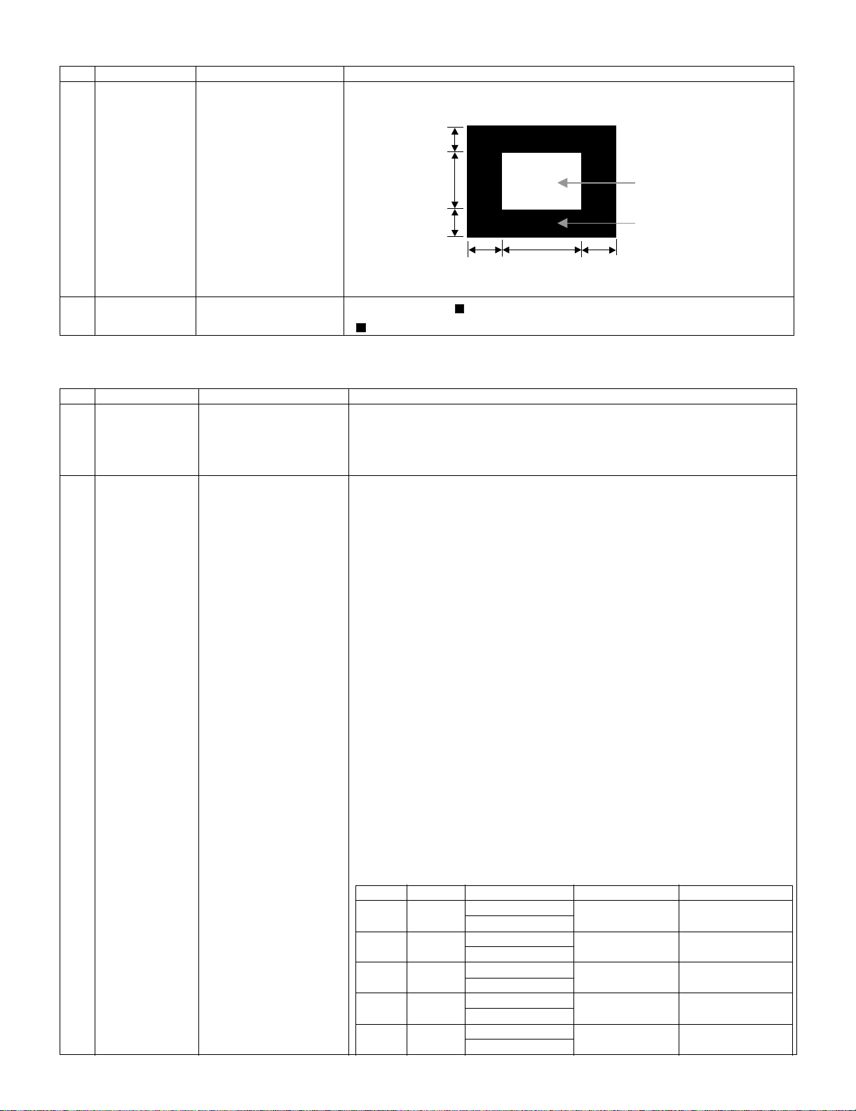
Parts marked with " " are important for maintaining the safety of the set. Be sure to replace these parts with specified ones for maintaining the
safety and performance of the set.
PARTS GUIDE
This document has been published to be used for
after sales service only.
The contents are subject to change without notice.
Page 2
LC-32D50U
LC-32D50U
SAFETY PRECAUTION
Service Manual
IMPORTANT SERVICE SAFETY PRECAUTION
Service work should be performed only by qualified service technicians who are thoroughly familiar with all safety checks and the
servicing guidelines which follow:
WARNING
1. For continued safety, no modification of any circuit should be
attempted.
2. Disconnect AC power before servicing.
CAUTION: FOR CONTINUED PROTECTION
AGAINST A RISK OF FIRE REPLACE ONLY WITH
SAME TYPE FUSE.
F701 (8A, 125V)
• Use an AC voltmeter having with 5000 ohm per volt, or higher, sensitivity or measure the AC voltage drop across the resistor.
• Connect the resistor connection to all exposed metal parts having a
return to the chassis (antenna, metal cabinet, screw heads, knobs
and control shafts, escutcheon, etc.) and measure the AC voltage
drop across the resistor.
All checks must be repeated with the AC cord plug connection
reversed. (If necessary, a nonpolarized adaptor plug must be used
only for the purpose of completing these checks.)
Any reading of 0.75 Vrms (this corresponds to 0.5 mA rms AC.) or
more is excessive and indicates a potential shock hazard which
must be corrected before returning the monitor to the owner.
F4701, F5701 (3A~, 250V, 115 C)
BEFORE RETURNING THE RECEIVER (Fire &
Shock Hazard)
Before returning the receiver to the user, perform the following
safety checks:
3. Inspect all lead dress to make certain that leads are not pinched,
and check that hardware is not lodged between the chassis and
other metal parts in the receiver.
4. Inspect all protective devices such as non-metallic control knobs,
insulation materials, cabinet backs, adjustment and compartment
covers or shields, isolation resistor-capacitor networks, mechanical
insulators, etc.
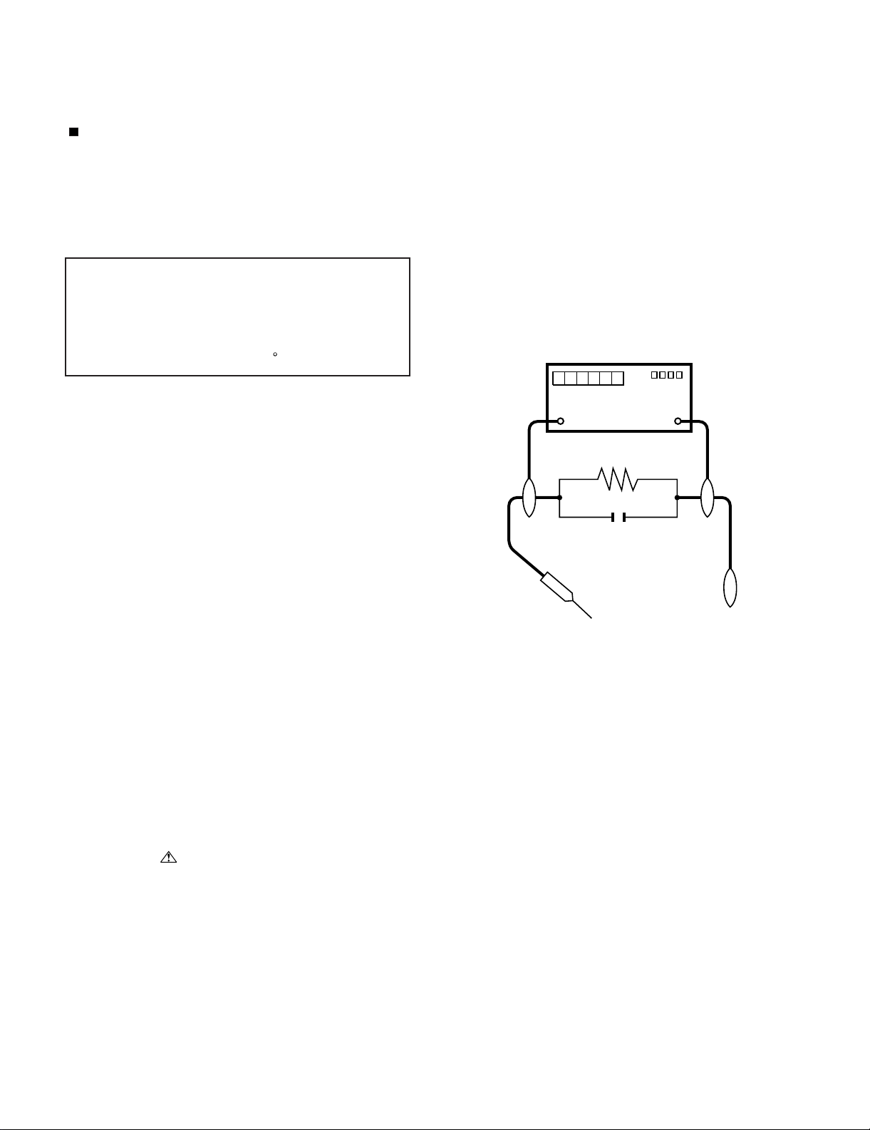
5. To be sure that no shock hazard exists, check for leakage current in
the following manner.
• Plug the AC cord directly into a 120 volt AC outlet.
• Using two clip leads, connect a 1.5k ohm, 10 watt resistor paralleled by a 0.15µF capacitor in series with all exposed metal cabinet
parts and a known earth ground, such as electrical conduit or electrical ground connected to an earth ground.
///////////////////////////////////////////////////////////////////////////////////////////////////////////////////////////////////////////////////////////////////////////////////////////////////////////////////////////////////////////
TO EXPOSED
METAL PARTS
DVM
AC SCALE
1.5k ohm
10W
0.15µF
TEST PROBE
CONNECT TO
KNOWN EARTH
GROUND
SAFETY NOTICE
Many electrical and mechanical parts in LCD color television have
special safety-related characteristics.
These characteristics are often not evident from visual inspection, nor
can protection afforded by them be necessarily increased by using
replacement components rated for higher voltage, wattage, etc.
Replacement parts which have these special safety characteristics are
identified in this manual; electrical components having such features
are identified by " " and shaded areas in the Replacement Parts
List and Schematic Diagrams.
For continued protection, replacement parts must be identical to those
used in the original circuit.
The use of a substitute replacement parts which do not have the same
safety characteristics as the factory recommended replacement parts
shown in this service manual, may create shock, fire or other hazards.
///////////////////////////////////////////////////////////////////////////////////////////////////////////////////////////////////////////////////////////////////////////////////////////////////////////////////////////////////////////
i
Page 3

LC-32D50U
PRECAUTIONS A PRENDRE LORS DE LA REPARATION
Ne peut effectuer la réparation qu' un technicien spécialisé qui s'est parfaitement accoutumé à toute vérification de sécurité et aux
conseils suivants.
AVERTISSEMENT
6. N'entreprendre aucune modification de tout circuit. C'est dangereux.
7. Débrancher le récepteur avant toute réparation.
PRECAUTION: POUR LAPROTECTION CONTINUE
CONTRE LES RISQUES D'INCENDIE,
REMPLACER LE FUSIBLE
F701 (8A, 125V),
F4701, F5701 (3A~, 250V, 115 C)
VERIFICATIONS CONTRE L'INCEN-DIE ET LE
CHOC ELECTRIQUE
Avant de rendre le récepteur à l'utilisateur, eff ectuer les vérifications suivantes.
8. Inspecter tous les faisceaux de câbles pour s'assurer que les fils ne
soient pas pincés ou qu'un outil ne soit pas placé entre le châssis
et les autres pièces métalliques du récepteur.
9. Inspecter tous les dispositifs de protection comme les boutons de
commande non-métalliques, les isolants, le dos du coffret, les couvercles ou blindages de réglage et de compartiment, les réseaux
de résistancecapacité, les isolateurs mécaniques, etc.
10.S'assurer qu'il n'y ait pas de danger d'électrocution en vérifiant la
fuite de courant, de la facon suivante:
• Brancher le cordon d'alimentation directem-ent à une prise de courant de 120V. (Ne pas utiliser de transformateur d'isolation pour cet
essai).
• A l'aide de deux fils à pinces, brancher une résistance de 1.5 k 10
watts en parallèle avec un condensateur de 0.15 F en série avec
toutes les pièces métalliques exposées du coffret et une terre connue comme une conduite électrique ou une prise de terre branchée
àlaterre.
• Utiliser un voltmètre CA d'une sensibilité d'au moins 5000 /V pour
mesurer la chute de tension en travers de la résistance.
• Toucher avec la sonde d'essai les pièces métalliques exposées qui
présentent une voie de retour au châssis (antenne, coffret métallique, tête des vis, arbres de commande et des boutons, écusson,
etc.) et mesurer la chute de tension CA en-travers de la résistance.
Toutes les vérifications doivent être refaites après avoir inversé la
fiche du cordon d'alimentation. (Si nécessaire, une prise d'adpatation non polarisée peut être utilisée dans le but de terminer ces
vérifications.)
Tous les courants mesurés ne doivent pas dépasser 0.5 mA.
Dans le cas contraire, il y a une possibilité de choc électrique qui
doit être supprimée avant de réndre le recepteur au client.
DVM
ECHELLE CA
1.5k ohm
10W
0.15
µ
SONDE D'ESSAI
F
AUX PIECES
METALLIQUES
EXPOSEES
///////////////////////////////////////////////////////////////////////////////////////////////////////////////////////////////////////////////////////////////////////////////////////////////////////////////////////////////////////////
BRANCHER A UNE
TERRE CONNUE
AVIS POUR LA SECURITE
De nombreuses pièces, électriques et mécaniques, dans les téléviseur
ACL présentent des caractéristiques spéciales relatives à la sécurité,
qui ne sont souvent pas évidentes à vue. Le degré de protection ne
peut pas être nécessairement augmentée en utilisant des pièces de
remplacement étalonnées pour haute tension, puissance, etc.
Les pièces de remplacement qui présentent ces caractéristiques sont
identifiées dans ce manuel; les pièces électriques qui présentent ces
particularités sont identifiées par la marque " " et hachurées dans
la liste des pièces de remplacement et les diagrammes schématiques.
Pour assurer la protection, ces pièces doivent être identiques à celles
utilisées dans le circuit d'origine. L'utilisation de pièces qui n'ont pas
les mêmes caractéristiques que les pièces recommandées par l'usine,
indiquées dans ce manuel, peut provoquer des électrocutions, incendies, radiations X ou autres accidents.
////////////////////////////////////////////////////////////////////////////////////////////////////////// /////////////////////////////////////////////////////////////////////////////////////////////////////////////////////////////////
ii
Page 4

LC-32D50U
Precautions for using lead-free solder
Employing lead-free solder
• "PWBs" of this model employs lead-free solder. The LF symbol indicates lead-free solder , and is attached on the PWBs and service manuals. The
alphabetical character following LF shows the type of lead-free solder.
Example:
L Fa
Indicates lead-free solder of tin, silver and copper.
Indicates lead-free solder of tin, silver and copper.
L F a/a
Using lead-free wire solder
• When fixing the PWB soldered with the lead-free solder, apply lead-free wire solder. Repairing with conventional lead wire solder may cause damage or accident due to cracks.
As the melting point of lead-free solder (Sn-Ag-Cu) is higher than the lead wire solder by 40 °C, we recommend you to use a dedicated soldering
bit, if you are not familiar with how to obtain lead-free wire solder or soldering bit, contact our service station or service branch in your area.
Soldering
• As the melting point of lead-free solder (Sn-Ag-Cu) is about 220 °C which is higher than the conventional lead solder by 40 °C, and as it has poor
solder wettability, you may be apt to keep the soldering bit in contact with the PWB for extended period of time. However, Since the land may be
peeled off or the maximum heat-resistance temperature of parts may be exceeded, remove the bit from the PWB as soon as you confirm the
steady soldering condition.
Lead-free solder contains more tin, and the end of the soldering bit may be easily corroded. Make sure to turn on and off the power of the bit as
required.
If a different type of solder stays on the tip of the soldering bit, it is alloyed with lead-free solder. Clean the bit after every use of it.
When the tip of the soldering bit is blackened during use, file it with steel wool or fine sandpaper.
• Be careful when replacing parts with polarity indication on the PWB silk.
Lead-free wire solder for servicing
Part No, Description Code
ZHNDAi123250E J φ0.3mm 250g(1roll) BL
ZHNDAi126500E J φ0.6mm 500g(1roll) BK
ZHNDAi12801KE J φ1.0mm 1kg(1roll) BM
iii
Page 5

LC-32D50U
CHAPTER 1. Specifications
Service Manual
[1] Specifications
Item Model: LC-32D50U
LC-32D50U
LCD panel
Number of dots
TV-standard
TV
Function
Receiving
Channel
Audio multiplex
Backlight
Audio out
Terminals
Rear
VHF/UHF
CATV
Digital Terrestrial
Broadcast (8VSB)
Digital cable*
(64/256 QAM)
INPUT1
INPUT2
INPUT3
INPUT4
INPUT5
Air ANTENNA
Cable ANTENNA
32" Advanced Super View & BLACK TFT LCD
3,147,264 dots (1366 x 768 x 3 dots)
American TV Standard ATSC/NTSC System
VHF 2-13ch, UHF 14-69ch
1-135ch (non-scrambled channel only)
2-69ch
1-135ch (non-scrambled channel only)
BTSC System
60,000 hours (at Backlight Standard position)
10W x 2
AV in, COMPONENT in
AV in, S-VIDEO in
HDMI in with HDCP
Audio in, HDMI in with HDCP
Audio in, DVI-I in with HDCP
75 Unbalance, F Type for VHF/UHF/Digital Air in x 1
75 Unbalance, F Type for CATV/Digital Cable in x 1
i.LINK
DIGITAL AUDIO OUTPUT
OUTPUT
OSD language
Power Requirement
Power Consumption
w/o stand
Weight
with stand
Dimension
(WxHxD)
w/o stand
with stand
Accessories
Operating temperature
IEEE1394 x 2 with DTCP (Compatible with DTVLink)
Optical Digital audio output x 1 (PCM/Dolby Digital)
Audio out
English/French/Spanish
AC120V,60Hz
178 W
39.7 lbs./18.0 kg
45.2 lbs./20.5 kg
1
/16x239/32x457/64inch
32
32
1
/
41
25
/
x
16
1
12
/64inch
x
64
Remote control unit(x 1), AC cord (x 1), “AAA” size battery (x 2), Cable clamp (x 1),
Cable tie(x 1), Stand unit (x 1), Operation manual (x 1)
+32°Fto+104°F(0°Cto+40°C)
* Emergency alert messages via Cable are unreceivable.
As part of policy of continuous improvement, SHARP reserves the right to make design and specification changes for product
•
improvement without prior notice. The performance specification figures indicated are nominal values of production units.
There may be some deviations from these values in individual units.
1 – 1
Page 6

LC-32D50U
LC-32D50U
CHAPTER 2. Operation Manual
[1] Operation Manual
HDMI terminal (INPUT 3)
HDMI terminal (INPUT 4)
i.LINK terminals
Service Manual
AIR IN terminal
CABLE IN terminal AC INPUT terminal
RS-232C terminal
Part names
TV (Rear)
Channel buttons
(CH /)
POWER button
INPUT button
/)
(INPUT 5)
DVI terminal
OUTPUT
DIGITAL AUDIO
terminal
DVI AUDIO
terminal
(INPUT 5)
terminals
AUDIO input
INPUT 1 terminals
INPUT 2
(INPUT 4)
terminals
terminals
AUDIO OUTPUT
OPC indicator*POWER
indicator**
OPC sensor*
TV (Front)
Part names
Volume buttons (VOL
2 – 1
Remote control sensor
NOTE
*OPC: Optical Picture Control.
**for TV status indicator.
Page 7

Hex key
LC-32D50U
Long screw
CAUTION
This will prevent it from being damaged.
Attaching the stand
• Before attaching (or detaching) stand, unplug the AC cord from the AC INPUT terminal.
QUICK REFERENCE
• Before performing work spread cushioning over the base area to lay the TV on.
• Attach the stand in the correct direction.
• The “REAR” label should be visible from the back of the TV. Refer to
the figure.
REAR
This side faces the rear.
• Incorrect installation of the stand may result in the TV falling over.
• Be sure to follow the instructions.
3.
1. Confirm the 8 screws supplied with the TV.
Insert the stand into the opening on the bottom of the
1
2
1
Insert and tighten the 4 long screws into the 4 holes on
the rear of the TV.
TV.
2
(used in step 3)
Long screws (x4)
(used in step 2)
Short screws (x4)
2. Attach the two parts of the stand unit to each other using
the 4 short screws and the hex key (supplied with the
product) as shown.
Soft cushion
Short screw
Hex key
NOTE
• To detach the stand, perform the steps in reverse order.
Part names
standby mode.
1 TV POWER: Switches the TV power on or enters
Remote control unit
equipment on and off.
2DISPLAY:Displays the channel information.
3 SOURCE POWER: Turns the power of the external
117
the external equipment.
50–9:Sets the channel.
4 External equipment operational buttons: Operates
6 • (DOT):
7AIR:Receives air signal.
2
18
3
8CABLE:Receives cable signal.
9VOL/:Sets the volume.
10 SURROUND: Selects Surround settings.
11 INFO: Displays the program information screen.
19
4
12 FREEZE: Sets the still image. Press again to return to
normal screen.
13 EXIT: Turns off the menu screen.
14 SLEEP: Sets the sleep timer.
5
15 i.LINK: Displays the i.LINK control panel.
16 AUDIO: Selects the MTS/SAP or the audio mode during
multi-channel audio broadcasts.
SAT, VCR, DVD and AUDIO operation. Indicator lights up
for the current mode.
17 FUNCTION: Switches the remote control for TV, CBL/
21
20
6
7228
* To enter the code registration mode, you need to press
FUNCTION and DISPLAY at the same time.
23
9
control unit will light. The lighting will turn off if no
18 LIGHT : When pressed all buttons on the remote
24
10
2 – 2
operations are performed within about 5 seconds. This
button is used for performing operations in low-light
25
11
situations.
19 VIEW MODE: Selects the screen size.
26
27
12
20 ENT: Jumps to a channel after selecting with the 0–9
buttons.
21 FLASHBACK: Returns to the previous channel or
28
13
external input mode.
22 INPUT: Selects a TV input source. (TV, INPUT 1, INPUT
29
2, INPUT 3, INPUT 4, INPUT 5, i.LINK)
23 CH / : Selects the channel.
30
24 MUTE: Mutes the sound.
25 CH LIST: Displays the channel list screen.
14
31
26 MENU: Displays the menu screen.
27 ////ENTER: Selects a desired item on the
15
screen.
28 RETURN: Returns to the previous menu screen.
16 32
29 FAVORITE CH
A, B, C, D: Selects four preset favorite channels in four
different categories.
While watching, you can toggle the selected channels by
pressing A, B, C and D
30 FAVORITE: Registers favorite channels.
31 CC: Displays captions from a closed-caption source.
32 AV MODE: Selects an audio or video setting. (AV mode:
STANDARD, MOVIE, GAME, USER, DYNAMIC (Fixed),
DYNAMIC. PC mode: STANDARD, MOVIE, GAME,
USER, DYNAMIC (Fixed), DYNAMIC, PC)
NOTE
• When using the remote control unit, point it at the TV.
Page 8
LC-32D50U
Basic adjustment settings
Picture
Menu items for HDMI/DVI
Picture
Menu items for TV/INPUT 1/INPUT 2
OPC
Backlight
OPC
Backlight
Contrast
Brightness
Color
Contrast
Brightness
Color
Tint
Sharpness
Advanced
Tint
Sharpness
Advanced
Color Temp.
Black
Monochrome
Color Temp.
Black
3D-Y/C
Audio
Film Mode
Range of OPC
Monochrome
Film Mode
Range of OPC
Audio
Treble
Bass
Treble
Balance
Surround
Bass
Balance
Power Control
Surround
Power Control
No Signal Off
No Operation Off
No Signal Off
No Operation Off
2 – 3
Setup
Setup
Input Skip
Input Signal
Auto Sync.
EZ Setup
CH Setup
Antenna Setup-DIGITAL
Input Label
Fine Sync.
Input Skip
Position
Picture Flip
Input Label
Parental CTRL
Standby Mode
Language
Position
Picture Flip
Standby Mode
Reset
Language
Reset
Option
Option
Audio Only
Digital Noise Reduction
Input Select
Audio Only
HDMI Setup
Output Select
Quick Shoot
Digital Noise Reduction
Input Select
Output Select
Quick Shoot
Digital Setup
Color System
Caption Setup
Program Title Display
Favorite CH
i.LINK Setup
Digital Setup
Audio Setup
i.LINK Setup
Page 9

LC-32D50U
CHAPTER 3. Dimensions
[1] Dimensions
243/32(612)
32
1
/16(814)
Service Manual
17
/
4
(115)
LC-32D50U
Unit: inch/(mm)
57
32
/
4
(124)
64
(651)
64
/
41
25
(200)
8
/
7
7
(591)
32
/
9
23
(115)
32
/
17
4
279/16(700.0)
7
7
/8(200)
64
/
35
15
(394.6)
(400)
4
/
3
15
121/64(305)
3 – 1
Page 10

LC-32D50U
LC-32D50U
CHAPTER 4. REMOVING OF MAJOR PARTS
Service Manual
[1] REMOVING OF MAJOR PARTS
1. Remove the SD Card Cover .
2. Remove the 4 lock screws and detach the Stand Base Ass'y.
1
3. Remove the 9 lock screws , 3 lock screws and detach the Rear Cabinet.
2 3
2
SD-Card
Cover
3
1
Rear
Cabinet
Stand Base Ass'y
4 – 1
Page 11

LC-32D50U
4. Remove the 2 lock screws and detach the Stand Assist Angle.
5. Remove the 4 lock screws and detach the Center Angle-L and R.
6. Remove the 3 lock screws and detach the Stand Cover.
7. Remove the 5 lock screws and detach the Stand Fix Angle.
4
5
6
7
5
Center Angel-L
Center Angel-R
5
Stand Fix Angle
Stand Cover
Stand Assist Angle
7
6
4
4 – 2
Page 12

LC-32D50U
8. Disconnect the connectors and , and detach the Speaker L and R.
9. Disconnect the connectors CN7501 and CN7502.
10.Remove the 5 lock screws and detach the MAIN Shield.
8
10
9
10
Main Shield
SpeakerR
C N 7501
C N 7502
8
9
Speaker L
4 – 3
Page 13

Top Cover Ass`y
Key Unit
LC-32D50U
12
P 2002
11
Coaxial
Cable
S C 1102
SC502
P 2602
P 2601
S C 1101
S C 501
P502
LED Unit
P2603
P9701
P9702
S C 1301
P 2704
P 2703
CN1 CN2
C N 5703
C N 5701
C N 5702
11.Disconnect the connectors, (P2002, P2601, P2602, P2603, P9701, P9702, SC1102, SC1101, SC1301, CN1, CN2, P2703, P502, CN5701,
CN5702, CN5703) and Remover the Coaxial Cable.
12.Remove the 2 lock screws and detach the LED Unit.
13.Remove the KEY Unit and Remove the 3 lock screws from the Top Cover Ass'y
11
12
4 – 4
Page 14

LC-32D50U
14.Remove the 4 lock screws and detach the PWB Ass'y.
15.Remove the 7 lock screws , 2 lock screws and detach the Jack Angle Long.
16.Remove the 5 lock screws and detach the IF Unit.
17.Remove the 6 lock screws and detach the POWER Supply Unit.
18.Remove the 5 lock screws and detach the MAIN Unit.
13
14-1 14-2
15
16
17
17
13
Main Unit
14-1
14-2
14-1
15
16
Power Supply Unit
Chassis
Jack Angle
Long
IF Unit
4 – 5
Page 15

LC-32D50U
19.Remove the 6 lock screws and Remove the 10 lock screws and detach the Center Assist Angle and Rug Angles and LCD Panel Module.
18
19 19 1918 18
Rug Angle
19
Center Assist Angle
19 1918 18
4 – 6
Page 16

LC-32D50U
LC-32D50U
CHAPTER 5. ADJUSTMENT PROCEDURE
Service Manual
[1] ADJUSTMENT PROCEDURE
The adjustment values are set to the optimum conditions at the factory before shipping. If a value should become improper or an adjustment is
required due to part replacement, make an adjustment according to the following procedure.
1. After replacement of any PWB unit and/or IC for repair, please note the following.
• When replacing the following units, make sure to prepare the new units loaded with updated software.
MAIN Unit: DUNTKD640FM13
IF Unit: DUNTKD643FM13
2. Upgrading of each microprocessor software
Caution: Never "POWER OFF" the unit when software upgrade is ongoing.
Otherwise the system may be damaged beyond recovery.
2.1. Software version upgrade
The model employs the following software.
•Main software
• Monitor microprocessor software
The main software and the monitor microprocessor software can be upgraded by using a general-purpose SD memory card.
The followings are the procedures for upgrading, explained separately for each of the main software, the monitor microprocessor software.
2.2. Main software version upgrade
Get ready before you start
• SD memory card of 32MB or higher capacity
• PC running on Windows 98/98SE/ME/2000/XP operating system
• SD memory card reader/writer with USB connectivity.
• SD memory card formatting software
(Downloadable at http://panasonic.jp/support/audio/sd/download/sd_formatter_e.html)
Preparations
To upgrade the main software, it is necessary to get ready the SD card for version upgrade before you start.
Follow the steps below and create the SD card for version upgrade.
1. Insert the SD card into the SD card reader/writer. Start the SD card formatting software. Click [Format].
(When you have the drive options, select the drive where the SD card is inserted before you proceed.)
5 – 1
Page 17

2. When the formatting is over, the following window appears. Click [OK].
3. Click [Exit] to finish the formatting.
NOTE: When you are done, take out the SD card once to make sure it is finished, and then insert it again.
LC-32D50U
4. Copy the binary image file D50UAxxx.SDC (named temporarily) for version upgrade to the root directory (folder) of the SD card drive.
NOTE: In the SD card drive, do not store other folders or unrelated files, or more than one binary image files for version upgrade.
Now the SD card for version upgrade is ready.
How to upgrade the software
5. Shut off the AC power (i.e. unplug the AC cord).
6. Insert the SD card for version upgrade (prepared as above) into the service socket located lower side from center at terminals, above S-VIDEO
terminal in the rear of the unit, in a way that the cut corner of the SD card comes at the upper side.
NOTE: If the SD card is inserted in a wrong way, the card will go deep inside the unit beyond retrieval. Take due care to insert the SD card correctly.
7. Turn on the AC power (i.e. plug in the AC cord).
8. After the unit startup, the system upgrade screen as shown below appears within 20-40 seconds.
SYSTEM UPGRADE
Program
12%
EEPROM
Part Init
U0601051OLD Version
NEW Version U0601241
M150
5 – 2
Page 18

LC-32D50U
9. Even a single failure in the process will trigger the upgrade failure screen as shown below. The word "NG" changes to red for the item failed.
NOTE: In the event of a failure, repeat the upgrading process. If the process repeatedly fails, it is likely that the hardware is troubled.
UPGRADE FAILURE
Program
24%
EEPROM
Part Init
NEW Version U0601241
10.Upon completion of the whole process, the upgrade success screen as shown below appear s. You can check the new software version on this
screen. The version information appears after the upgrade is complete.
UPGRADE SUCCESS
Program
100%
EEPROM
Part Init
NG
NG
U0601051OLD Version
NG
NG
U0601241Main Version
11.Shut off the AC power to the unit (unplug the AC cord), and remove the SD card for version upgrade.
12.Now the software version upgrade is complete.
NOTE: When you are done with the software version upgrade, start the set, go to the top page of the adjustment process screen and check the main
software version information.
5 – 3
Page 19

LC-32D50U
2.3. Monitor microprocessor software version upgrade
NOTE: If "Monitor version" in the process me nu is "2.00M", the monitor microprocessor software can not be rewritten (because IC2002 has been
replaced with the mask type).
Get ready before you begin
Get ready the same items as listed in the "Main software version upgrade".
Preparation
Create the SD card for monitor microprocessor software version upgrade in the same manner as explained in the "Main software version upgrade".
Copy the binary image file M150Mxxx.SDC (named temporarily) for monitor microprocessor software version upgrade to the SD card drive.
How to upgrade the software
1. Shut off the AC power to the unit (i.e. unplug the AC cord).
2. Insert the SD card for version upgrade (prepared as above) into the service socket located lower side from center at terminals, above S-VIDEO
terminal in the rear of the unit, in a way that the cut corner of the SD card comes at the upper side.
NOTE: If the SD card is inserted in a wrong way, the card will go deep inside the unit beyond retrieval. Take due care to insert the SD card correctly.
3. Turn on the AC power (i.e. plug in the AC cord).
CAUTION:The moment this operation is done, the upgrading of the monitor microprocessor software starts. While the upgrade is ongoing,
never power off the unit. Otherwise the upgrade will fail and the s ystem may have a serious damage beyond recov ery (inability
to start).
4. After the unit startup, the system upgrade screen as shown below appears within 10-30 seconds.
MONITOR UPGRADE
Program
12%
1.00OLD Version
NEW Version 1.02
NG
M150
5. A failure in the process will trigger the upgrade failure screen. The word "NG" changes to red for the item failed.
NOTE: In the event of a failure, repeat the upgrading process. If the process repeatedly fails, it is likely that the hardware is troubled.
6. Upon completion of the whole process,the upgrade success screen as sho wn below appears.You can check the new software version on this
screen. The version information appears after the upgrade is complete.
7. Shut off the AC power to the unit (unplug the AC cord), and remove the SD card for version upgrade.
8. Now the software version upgrade is complete.
NOTE: When you are done with the software version upgrade, start the set, go to the top page of the adjustment process screen and check the mon-
itor microprocessor software version information.
2.4. Video signal adjustment procedure
1) Image adjustment
1. Device check
Before adjustment, make sure that the adjusting device and signal source are set for the Sharp LCD US.
Signal generator level adjustment check (Adjustment to the specified level)
• Composite signal : 0.714Vp-p ± 0.02Vp-p (Pedestal to white level)
• 15K component signal : Y level : 0.714Vp-p ± 0.02Vp-p (Pedestal to white level)
PB, PR level : 0.7Vp-p ± 0.02Vp-p
• 33K component signal : Y level : 0.7Vp-p ± 0.02Vp-p (Pedestal to white level)
PB, PR level : 0.7Vp-p ± 0.02Vp-p
• DVI-I (Analog RGB) signal : RGB level : 0.7Vp-p ± 0.02Vp-p (Pedestal to white level)
5 – 4
Page 20
LC-32D50U
2. Entering the adjustment process mode
Adjustment item Adjustment conditions Adjustment procedure
1 Adjustment pro-
cess mode
3. N358 composite signal / Tuner adjustment
Adjustment item Adjustment conditions Adjustment procedure
1 Adjustment N358 signal
US-10ch
Enter the process adjustment mode using the process adjustment remote control.
Feed the N358 color bar signal (75% color saturation) to VIDEO 1 input.
Feed the RF signal (by use of US-10ch) to TUNER.
[Video input signal] [US-10CH]
75% color saturation
100% white 100% white
2 Auto adjustment
performance
4. Component 15K signal adjustment
Adjustment item Adjustment conditions Adjustment procedure
1 Adjustment 480i signal Feed the 100% color bar signal to VIDEO 1 component input.
Page 3
Bring the cursor on [ N358 ALL ADJ] and press [ENTER].
[ N358 ALL ADJ FINISH] appears when finished.
480i
100% color bar signal
100% white
2 Auto adjustment
performance
5. Component 33K signal adjustment
Adjustment item Adjustment conditions Adjustment procedure
1 Adjustment 1080i signal Feed the 100% color bar signal to VIDEO 1 component input.
Page 5
Bring the cursor on [ COMP 15K MAIN ADJ] and press [ENTER].
[ COMP 15K MAIN ADJ FINISH] appears when finished.
0% black
2 Auto adjustment
performance
Page 6
1080i
100% color bar signal
100% white
Bring the cursor on [ HDTV ADJ] and press [ENTER].
[ HDTV ADJ FINISH] appears when finished.
0% black
5 – 5
Page 21
6. DVI-I (analog) signal adjustment
Adjustment item Adjustment conditions Adjustment procedure
1 Adjustment DVI-I (analog)
signal: XGA
(1024 x 768) 60Hz
SYNC:
HV separate
Feed the XGA (100%) white 1/2 window to DVI-I (analog) .
1/4
LC-32D50U
1/2
1/4
1/4
2 Auto adjustment
performance
Bring the cursor on [ DVI ANALOG ADJ] and press [ENTER].
[ DVI ANALOG ADJ OK] appears when finished.
2.5. Adjustment of white balance
1. White balance adjustment
Adjustment item Adjustment conditions Adjustment procedure
1 Setting 1) Apply the following settings to the set.
2 Execution of auto
adjustment
[Command]
Process mode
KRSW0001
KKT10037
Setting
KYOF0000
OSDS0001
SBSL0016
Multipoint adjustment mode
MSET0001
Adjustment value initialization
MSET0004
Point 6
LEV60944
MG6G****
MG6B****
MG6R****
AV MODE: [DYNAMIC]
Backlight: +16
Aging Time: Min. 60 minutes
2) Connect a white balance adjustment jig and the set.
[Adjustment method]
1) Send the “monitor adjustment process” code with the R/C.
2) Set the point 6 to the specified gradation. Set the strongest color as the fixed color
and adjust RGB to the standard value by minus adjustment.
3) Set the point 5 to the specified gradation. Set the correction value of G [(Initial value
of point 5) x (G value of point 6) / (Initial value of point 6)] and adjust RB to the standard value.
4) Set the point 4 to the specified gradation. Set the correction value of G [(Initial value
of point 4) x (G value of point 6) / (Initial value of point 6)] and adjust RB to the standard value.
5) Set the point 3 to the specified gradation. Set the correction value of G [(Initial value
of point 3) x (G value of point 6) / (Initial value of point 6)] and adjust RB to the standard value.
6) Set the point 2 to the specified gradation. Set the correction value of G [(Initial value
of point 2) x (G value of point 6) / (Initial value of point 6)] and adjust RB to the standard value.
7) Set the point 1 to the specified gradation. Set the correction value of G [(Initial value
of point 1) x (G value of point 6) / (Initial value of point 6)] and adjust RB to the standard value.
8) Write the adjustment values with the MSET0003 command and turn off AC power.
* Initial value of each point: Set gradation level x 4
1/2
100% White
0% Black
1/4
Point 5
LEV50800
MG5G****
MG5B****
MG5R****
Point 4 Level Standard value Adjustment spec Test spec
LEV40576 Point 6 944 X=0.272 ±0.0012 ±0.0020
MG4G**** y=0.277
MG4B**** Point 5 800 X=0.272 ±0.0012 ±0.0020
MG4R**** y=0.277
Point 3 y=0.277
LEV30464 Point 3 464 X=0.272 ±0.0012 ±0.0020
MG3G**** y=0.277
MG3B**** Point 2 264 X=0.272 ±0.0012 ±0.0020
MG3R**** y=0.277
[Adjustment values]
•Conform to “Standard set” submitted by Engineering Department.
[LC-32D50U] Teaching set
[Adjustment standard values] Measuring device: [Minolta CA-210 ] technical measuring
device
Point 4 576 X=0.272 ±0.0012 ±0.0020
5 – 6
Page 22

LC-32D50U
Adjustment item Adjustment conditions Adjustment procedure
Point 2 Point 1 200 X=0.272 ±0.0020 ±0.0035
LEV20264 y=0.277
MG2G****
MG2B****
MG2R****
Point 1
LEV10200
MG1G****
MG1B****
MG1R****
Writing
MSET0003
Note
2.6. Key writing
1. EDID writing (Main PWB: QPWBXD640WJZZ DVI input terminal/HDMI input terminal)
Adjustment item Adjustment conditions Adjustment procedure
1 DVI EDID writing File version check 1) Write the EDID data for DVI into IC1505 mounted on the
2 HDMI EDID writ-
ing
Inspection mode
File version check
Test conditions of the set:
2
AV MODE: [DYNAMIC] (Reset)
Monochro: ON
Aging Time: Min. 60 minutes
main PWB with the checker.
TL1514 ••• I2C clock, TL1515 ••• I2C data
TL1516 ••• 5V, TL1517 ••• GND
TL1536••• write protection (H: WP, Low: write enable)
1) Write the EDID data for HDMI into IC1501/IC1502
mounted on the main PWB with the checker.
TL1508/1510••• I2C clock, TL1509/1511••• I2C data
TL1512/1513••• 5V, TL1519/1518••• GND
TL1534/1535••• write protection (H: WP, Low: write
enable)
2) Perform data writing before the checker inspects HDMI.
(If no data has been written, HDMI does not function.)
2. DTCP key writing
Adjustment item Adjustment conditions Adjustment procedure
DTCP key writing
for i.Link
File version check 1) Write the DTCP key into IC8453 mounted on the main
PWB with the checker.
Set TL8453(I2C EXT) to L.
Connect TL8454(SCL)/TL8455(SDA) to the I2C bus.
2) Write the specified data into the specified address (A8).
• Use the second-generation DTCP device key.
• Conform to the internal key management agreement to
manage the DTCP device key.
• Follow [DTCP device key operation check manual] to
check operation.
• For the inspection or production, start in the process
start mode or inspection start mode.
• For details, refer to [Precautions for production].
5 – 7
Page 23

3. Adjustment sequence (adjustment according to the G adjustment value of gradation 6)
* Make sure the adjusting point gradations are correct since they are different for each model.
PC Set
Set the light level to MAX with the light control command
(SBSL0016 for 45).
SBSL0016
Setting is complete.
OK
Multipoint adjustment mode setting
MSET0001
Multipoint adjustment mode is set.
OK
Initialize adjustment values.
MSET0004
Initialization is done.
OK
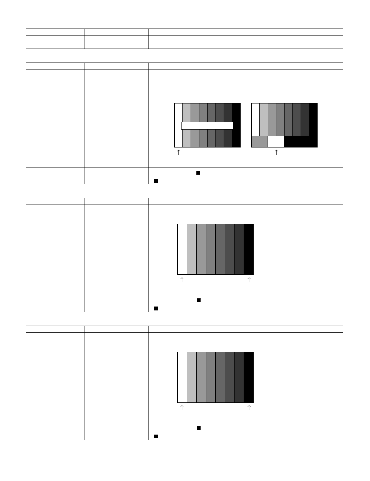
Adjustment gradation setting (point 6 = 236 gradation adjustment*)
LEV60944
Adjustment values are set.
OK
LC-32D50U
Pattern display
Repeat until RGB
become the target
values.
Adjust RGB to the target xy values.
MG6RXXXX
MG6GXXXX
MG6BXXXX
* XXXX indicates the adjusted values between 0000 and 1023
(4 digit decimal number with zero fill).
* In order to adjust by reducing the value, set the strongest color
as the fixed color.
* The default adjustment value of RGB is the parameter value of
the LEV6 command multiplied by 2.
The adjustment value is
reflected in the image.
Adjustment values are set.
OK
Adjustment gradation setting (point 5 = 200 gradation adjustment*)
LEV50800
Pattern display
Adjustment values are set.
OK
Correction of G value
MG5GXXXX
When G is changed at gradation 6, calculate the ratio of the
change and set the following value to XXXX: (the value set with
LEV5)x2x(theratio).
Adjustment values are set.
OK
5 – 8
Page 24

LC-32D50U
Start measurement
Repeat until RGB
become the target
values.
PC Set
Adjust RB to the target xy values.
MG5RXXXX
MG5BXXXX
* XXXX indicates the adjusted values between 0000 and 1023
(4 digit decimal number with zero fill).
*Gisfixed.
* The default adjustment value of RGB is the parameter value
of the LEV5 command multiplied by 2.
The adjustment value is
reflected in the image.
Adjustment values are set.
OK
Adjustment gradation setting (point 4 = 144 gradation adjustment*)
LEV40576
Pattern display
Adjustment values are set.
OK
Correction of G value
MG4GXXXX
When G is changed at gradation 6, calculate the ratio of the
change and set the following value to XXXX: (the value set with
LEV4)x2x(theratio).
Start measurement
Repeat until RGB
become the target
values.
Adjustment values are set.
OK
Adjust RB to the target xy values.
MG4RXXXX
MG4BXXXX
* XXXX indicates the adjusted values between 0000 and 1023
(4 digit decimal number with zero fill).
*Gisfixed.
* The default adjustment value of RGB is the parameter value of
the LEV4 command multiplied by 2.
The adjustment value is
reflected in the image.
Adjustment values are set.
OK
Adjustment gradation setting (point 3 = 116 gradation adjustment*)
LEV30464
Pattern display
Adjustment values are set.
OK
Correction of G value
MG3GXXXX
When G is changed at gradation 6, calculate the ratio of the
change and set the following value to XXXX: (the value set with
LEV3)x2x(theratio).
Adjustment values are set.
OK
5 – 9
Page 25
Start measurement
Repeat until RGB
become the target
values.
LC-32D50U
PC Set
Adjust RB to the target xy values.
MG3RXXXX
MG3BXXXX
* XXXX indicates the adjusted values between 0000 and 1023
(4 digit decimal number with zero fill).
* G is fixed.
* The default adjustment value of RGB is the parameter value of
the LEV3 command multiplied by 2.
The adjustment value is
reflected in the image.
Adjustment values are set.
OK
Adjustment gradation setting (point 2 = 66 gradation adjustment*)
LEV20264
Pattern display
Adjustment values are set.
OK
Correction of G value
MG2GXXXX
When G is changed at gradation 6, calculate the ratio of the
change and set the following value to XXXX: (the value set with
LEV2)x2x(theratio).
Start measurement
Repeat until RGB
become the target
values.
Adjustment values are set.
OK
Adjust RB to the target xy values.
MG2RXXXX
MG2BXXXX
* XXXX indicates the adjusted values between 0000 and 1023
(4 digit decimal number with zero fill).
* G is fixed.
* The default adjustment value of RGB is the parameter value of
the LEV2 command multiplied by 2.
The adjustment value is
reflected in the image.
Adjustment values are set.
OK
Adjustment gradation setting (point 1 = 50 gradation adjustment*)
LEV10200
Pattern display
Adjustment values are set.
OK
Correction of G value
MG1GXXXX
When G is changed at gradation 6, calculate the ratio of the
change and set the following value to XXXX: (the value set with
LEV1)x2x(theratio).
5 – 10
Adjustment values are set.
OK
Page 26

LC-32D50U
Start measurement
Repeat until RGB
become the target
values.
PC Set
Adjust RB to the target xy values.
MG1RXXXX
MG1BXXXX
* XXXX indicates the adjusted values between 0000 and 1023
(4 digit decimal number with zero fill).
* G is fixed.
* The default adjustment value of RGB is the parameter value of
the LEV1 command multiplied by 2.
The adjustment value is
reflected in the image.
Adjustment values are set.
OK
Writing of adjusted values
MSET0003
Writing is complete.
OK
Deleting adjustment patterns
MSET0000
Deletion is complete.
OK
Completion of adjustment
2.7. Initialization to factory settings
After the shipping setting, pull off the AC cord.
NOTE: Never turn on the power after the shipping setting. If power is turned on, perform the shipping setting again.
Adjustment item Adjustment conditions Adjustment procedure
1 Initialization It turns off with AC power supply. Place the cursor on the [INDUSTRY INIT] row, set "ON" with
[+] or [-] of the [VOL] key, and press the [ENT] key.
Version confirmation screen appears.
[SUCCESS] on a green line indicates that the setting is successfully completed.
(In case of an error, [ERROR] and an error code appear on
a red line.)
Turn off the AC power.
1. User setting
2. Channel data (e.g. broadcast frequencies)
3. Password data
4. Operation time
5. Auto installation flag
6. V-CHIP block setting
5 – 11
Page 27

2.8. Menu list in process A mode
Page Line Item
1 MAIN Version Main microcomputer software version
BOOT Version
Monitor Version Monitor microcomputer software version
EQ DATA CHECKSUM Sound parameter checksum
TEMPERATURE Read value of temperature sensor
LAMP ERROR Number of lamp error
NORMAL STANDBY CAUSE Reasons of standby at normal time
ERROR STANDBY CAUSE Reasons of standby in the event of error
2 INDUSTRY INIT(+Cause) Initialization to factory settings(including clearing Sandby Cause data)
INDUSTRY INIT Initialization to factory settings
HOTELMODE Activate/deactivate the hotel mode
Center Acutime Main microcomputer operating time
RESET Reset main microcomputer operating time
Lamp error rest
BacklightAcutime Backlight lighting time
RESET Reset backlight lighting time
LAMP ERROR RESET
VIC XPOS x-coordinate for reading image data
VIC YPOS y-coordinate for reading image data
VIC COLOR Specification of color for reading image data
VIC SIGNAL TYPE Specification of signal for reading image data
VIC READ On/Off of image data read operation
LC-32D50U
3 N358 ALL ADJ Auto adjustment of NTSC and TUNER signals
N358 MAIN ADJ Auto adjustment of NTSC signal
TUNER DAC ADJ Auto adjustment of TUNER
N358 MAIN CONTRAST NTSC contrast adjustment
TUNER A DAC TUNER DAC adjustment
4 TUNER VCHIP TEST(69ch) Execute TUNER TEST
TUNER VCHIP TEST(7ch)
TUNER VCHIP TEST(10ch)
TUNER VCHIP TEST(15ch)
5 COMP15K MAIN ADJ Auto adjustment of component 15k
COMP15K MAIN CONTRAST Component 15k contrast adjustment
6 HDTV ADJ HDTV auto adjustment
CONTRAST HDTV contrast adjustment
Cb GAIN HDTV CB gain adjustment
Cr GAIN HDTV CR gain adjustment
HDTV Y OFFSET HDTV Y offset adjustment
HDTV Cb OFFSET HDTV CB offset adjustment
HDTV Cr OFFSET HDTV CR offset adjustment
7 DVI ANALOG DVI ANALOG adjustment
R CUTOFF R CUTOFF adjustment value
G CUTOFF G CUTOFF adjustment value
B CUTOFF B CUTOFF adjustment value
R DRIVE R DRIVE adjustment value
G DRIVE G DRIVE adjustment value
B DRIVE B DRIVE adjustment value
8 MONITOR GAMMA IN 1 White balance adjustment IN-Point1
MONITOR GAMMA IN 2 White balance adjustment IN-Point2
MONITOR GAMMA IN 3 White balance adjustment IN-Point3
MONITOR GAMMA IN 4 White balance adjustment IN-Point4
MONITOR GAMMA IN 5 White balance adjustment IN-Point5
MONITOR GAMMA IN 6 White balance adjustment IN-Point6
GAMMA WRITE Write adjustment values
GAMMA RESET Reset adjustment values
5 – 12
Page 28

LC-32D50U
Page Line Item
9 MONITOR GAMMA R 1 White balance adjustment OUT R-Point1
MONITOR GAMMA G 1 White balance adjustment OUT G-Point1
MONITOR GAMMA B 1 White balance adjustment OUT B-Point1
MONITOR GAMMA R 2 White balance adjustment OUT R-Point2
MONITOR GAMMA G 2 White balance adjustment OUT G-Point2
MONITOR GAMMA B 2 White balance adjustment OUT B-Point2
MONITOR GAMMA R 3 White balance adjustment OUT R-Point3
MONITOR GAMMA G 3 White balance adjustment OUT G-Point3
MONITOR GAMMA B 3 White balance adjustment OUT B-Point3
GAMMA WRITE Write adjustment values
GAMMA RESET Reset adjustment values
10 MONITOR GAMMA R 4 White balance adjustment OUT R-Point4
MONITOR GAMMA G 4 White balance adjustment OUT G-Point4
MONITOR GAMMA B 4 White balance adjustment OUT B-Point4
MONITOR GAMMA R 5 White balance adjustment OUT R-Point5
MONITOR GAMMA G 5 White balance adjustment OUT G-Point5
MONITOR GAMMA B 5 White balance adjustment OUT B-Point5
MONITOR GAMMA R 6 White balance adjustment OUT R-Point6
MONITOR GAMMA G 6 White balance adjustment OUT G-Point6
MONITOR GAMMA B 6 White balance adjustment OUT B-Point6
GAMMA WRITE Write adjustment values
GAMMA RESET Reset adjustment values
11 AUDIO SELECT Select sound parameter data(ROM/EEP)
INPUT_TRIM_SP
INPUT_TRIM_HP
CLIPPER_LEVEL
ANGLE
MASTER_VOLUME
SCART_PRESCALE
FM_AM_PRESCALE
I2S1_PRESCALE
SCART1_VOLUME
SCART2_VOLUME
12 AIN1_ADC_VOLUME
AIN2_ADC_VOLUME
AIN3_ADC_VOLUME
AIN4_ADC_VOLUME
AIN5_ADC_VOLUME
AIN6_ADC_VOLUME
13 SUB_VOLUME_SURROUND
SUB_VOLUME_FLAT
SUB_VOLUME_EQ
SUB_VOLUME_HP
SUB_VOLUME_HP_CENTER
SP
SUB_VOLUME_CENTERSP_
EQ
SUB_VOLUME_CENTERSP_
FLAT
BBE_HF_ADJUST
BBE_LEVEL
BBE_MACH3_F0
BBE_MACH3_Q
BBE_MACH3_GAIN
14 EQ_MODE
PEQ1_F0
PEQ1_Q
PEQ1_GAIN
PEQ2_F0
PEQ2_Q
5 – 13
Page 29

Page Line Item
14 PEQ2_GAIN
PEQ3_F0
PEQ3_Q
PEQ3_GAIN
PEQ4_F0
PEQ4_Q
PEQ4_GAIN
15 PEQ5_F0
PEQ5_Q
PEQ5_GAIN
EALA_GAIN
16 BRIGHTNESS DA0
BRIGHTNESS DA1
BRIGHTNESS DA2
BRIGHTNESS DA3
BRIGHTNESS DA4
BRIGHTNESS DA5
BRIGHTNESS DA6
BRIGHTNESS DA7
BRIGHTNESS DA8
BRIGHTNESS DA9
BRIGHTNESS DA10
BRIGHTNESS DA11
LC-32D50U
17 BRIGHTNESS DA12
BRIGHTNESS DA13
BRIGHTNESS DA14
BRIGHTNESS DA15
BRIGHTNESS DA16
BRIGHTNESS DA17
BRIGHTNESS DA18
BRIGHTNESS DA19
BRIGHTNESS DA20
BRIGHTNESS DA21
BRIGHTNESS DA22
18 BRIGHTNESS DA23
BRIGHTNESS DA24
BRIGHTNESS DA25
BRIGHTNESS DA26
BRIGHTNESS DA27
BRIGHTNESS DA28
BRIGHTNESS DA29
BRIGHTNESS DA30
BRIGHTNESS DA31
BRIGHTNESS DA32
19 OPC33 ADLEVEL 0
OPC33 ADLEVEL 1
OPC33 ADLEVEL 2
OPC33 ADLEVEL 3
OPC33 ADLEVEL 4
OPC33 ADLEVEL 5
OPC33 ADLEVEL 6
OPC33 ADLEVEL 7
OPC33 ADLEVEL 8
OPC33 ADLEVEL 9
OPC33 ADLEVEL 10
OPC33 ADLEVEL 11
20 OPC33 ADLEVEL 12
OPC33 ADLEVEL 13
5 – 14
Page 30
LC-32D50U
Page Line Item
20 OPC33 ADLEVEL 14
OPC33 ADLEVEL 15
OPC33 ADLEVEL 16
OPC33 ADLEVEL 17
OPC33 ADLEVEL 18
OPC33 ADLEVEL 19
OPC33 ADLEVEL 20
OPC33 ADLEVEL 21
OPC33 ADLEVEL 22
21 OPC33 ADLEVEL 23
OPC33 ADLEVEL 24
OPC33 ADLEVEL 25
OPC33 ADLEVEL 26
OPC33 ADLEVEL 27
OPC33 ADLEVEL 28
OPC33 ADLEVEL 29
OPC33 ADLEVEL 30
OPC33 ADLEVEL 31
22 V6 OS THERMO 1
V6 OS THERMO 2
V6 OS THERMO 3
V6 OS THERMO 4
V6 OS THERMO 5
V6 OS THERMO 6
V6 OS THERMO 7
23 V5 OS THERMO 1
V5 OS THERMO 2
V5 OS THERMO 3
V5 OS THERMO 4
V5 OS THERMO 5
V5 OS THERMO 6
V5 OS THERMO 7
24 MONITOR TIME OUT
MONITOR MAX TEMP
MONITOR STANDBY CAUSE
25 LCD TEST PATTERN
26 KEY LOCK(1217)
KOUTEI AREA ALL CLEAR
A MODE AREA CLEAR
BACKUP AREA CLEAR
B MODE AREA CLEAR
EXECUTION
27 EEP SAVE
EEP RECOVER
STANDBY CAUSE RESET
2.9. Code list for St andby Cause
Code Indication Description
1 RC_STNBY /* Standby set by remote control */
2 E_CCKMVT /* Abnormal voltage of CCKM line detected */
5 OUT_OF_R "/* While a PC display is on, unspecified input continued long time. */"
6 NO_OPERT /* Off caused by no operation */
7 NO_SIGNA /* Off caused by no signal */
8 PC_MODE1 /* Set by the PC power management mode 1 */
9 PC_MODE2 /* Set by the PC power management mode 2 */
A SLEEP_TM /* Set by off timer */
B E_NOMONI /* Incompatible monitor is connected to the AVC center. */
5 – 15
Page 31

Code Indication Description
C OFF_232C /* Set by the command from RS232C */
E AVC_TACT /* Set by the front switch at the AVC center */
F BSBOOKED /* The pre-set time has passed since TV was turned on from standby by the BS timer. */
10 E_AVCFAN /* Fan failure at the AVC center */
11 E_BSSUBM /* Communication failure with the BS sub microcomputer (Not used) */
12 E_CVICIC /* CVIC failure */
13 E_AVCTMP /* Abnormal temperature at the AVC center */
14 E_1BITAU /* 1Bit-AMP failure */
15 E_MONIPW /* Monitor main power failure detected */
16 E_MONITR /* Monitor problem detected */
17 E_FNLOCK /* Fan lock for North America */
40 /* Failure in Digital Standby */
LC-32D50U
5 – 16
Page 32

LC-32D50U
1
LC-32D50U
CHAPTER 6. TROUBLESHOOTING TABLE
Service Manual
[1] TROUBLESHOOTING TABLE
<Power supply>
No power supply (Front LED does not light up) and no power-up even is turned on (Front LED light up to blue)
Is the AC cord connected? NO Connect the AC cord and turn on the power.
YES
Are the harness and FFC connected properly? NO Connect the harness and FFC properly.
YES
Are F701 normal?
YES
Is the voltage of C4701/C4702/C4703 approx.
160V?
NO
NO Check if VZ701, R701, R702, R703 and DS4701 are normal.
If the fuse is blown when turning on the power after replacing F701, replace
VZ701, DS4701, F4701/F4702, F5701, Q4701/Q4702, Q5701, IC4701 and
IC5701, then recheck.
YES
Is BU5V supplied? NO
Do the primary side and secondary side of T5701 oscillate normally?
YES
Are F5702, D5705, IC5706 and D5717 out
of order?
Are there defective parts on the
primary side? Is the output on the
NO
secondary side short-circuited?
YES
Are UR6V/UR10V/UR13V supplied? NO Does PS_ON (pin 1 of CN5702) become High (approx. 3.3V)?
YES
Check the regulator circuit of UR6V, rectifier
circuit of UR13V and DC/DC circuit of
Is the unit set to STANDBY
MODE2? Is the main unit normal?
NO
UR10V.
YES
Is 24V supplied? NO Do the primary side and secondary side of T4701 oscillate normally?
YES NO
Are D4705/D4706 out of order? Are there defective parts on the
primary side? Is the output on the
secondary side short-circuited?
YES
Is PNL5V supplied? NO Does PNL_POW (pin 4 of CN5702) become High (approx. 3.3V)?
YES
Check the DC/DC circuit of PNL5V? Is the main unit normal?
Turn on the power again, and check if the unit
works normally.
Remarks
State of the set
STDBY
MODE1 High High 5V 6V 10V 13V 5V 24V
MODE2LowLow5V-----
PS_ON
(CN5702 )
1
PNL_POW
(CN5702 )
4 5
BU5V
(CN5702 )
UR6V
(CN5701 )
1
UR10V
(CN5701 )
7
UR13V
(CN5701 )
11
(CN5701 )
PNL5V
3
(CN5703 )
24V
Power ON High High 5V 6V 10V 13V 5V 24V
6 – 1
Page 33

No audio output during UHF/VHF reception
Is Video output during UHF/VHF reception normal? NO Check the tuner and RF-SW (UNT 501)
YES
Is SIF output from the tuner (TU1101_Pin3) normal? NO Check the tuner and peripheral circuits.
YES
Is input signal fed to pin 21 (SOUNDIF 1) of IC1401 (SIF Demodulator) normal?
YES
Are audio signals from pins 29 and 30 (SC2_OUTL/R) of IC1401
to pins 51 and 52 of IC1403 (CODEC) normal?
YES
Are audio outputs (A-OUT_L/R) of pins 38 and 39 of IC1403 nor-
mal?
YES
Is audio input from pins 38 and 39 of IC1403 to pins 11 and 15 of
IC2701(STEREO_AMP) normal?
NO Check the filter circuits (Q1144 and Q1102-3) and peripheral cir-
cuits.
NO Check between pins 29 and 30 (SC2_OUTL/R) of IC1401 and
pins 51 and 52 of IC1403 (CODEC).
NO Are the LRCK, BICK, SDTO and SDTI signals sent from IC1403
to IC1406 (DSP) normally?
YES
Check IC1403 and peripheral circuits.
NO Check the circuits between pins 38 and 39 of IC1403 and pins 1 1
and 15 of IC2701. (MUTE circuits: Q1306-8)
LC-32D50U
YES
Is audio output from IC2701 normal? NO Check IC2701 and peripheral circuits.
YES
Is the speaker switching circuit (T2701)
YES
Check the connector (P2703) of AV_UNIT and around the speakers.
No monitor audio output
Is monitor audio output set to "Variable"? YES Reset monitor audio output to "Fixed".
NO
Are audio output pins 40 and 41 of IC1403 (CODEC) normal? NO Check IC1403 and peripheral circuits.
YES
Are audio output pins 7 and 1 of IC1407 (Buffer_AMP) normal? NO Check IC1407 and peripheral circuits.
YES
Check between IC1407 and MONITOR OUTPUT terminal (pins
10 and 16 of J502).
6 – 2
Page 34

LC-32D50U
No audio output from external input
<<INPUT-1>>
Is L-ch audio signal fed from pin 12 of input terminal J501 to pin 53 of IC1403?
Is R-ch audio signal fed from pin 18 of input terminal J501 to pin 54 of IC1403?
<<INPUT-2>>
Is L-ch audio signal fed from pin 10 of input terminal J501 to pin 57 of IC1403?
Is R-ch audio signal fed from pin 16 of input terminal J501 to pin 58 of IC1403?
<<HDMI>> [INPUT-3/INPUT4 (Digital audio mode)]
Is digital audio signal (HDMI_SPDIF) fed from pin 70 of IC1508 to pin 2 of IC1401?
<<HDMI>> [INPUT-4 (Analog audio mode)]
Is L-ch audio signal fed from pin 3 of input terminal J1501 to pin 59 of IC1403?
Is R-ch audio signal fed from pin 2 of input terminal J1501 to pin 60 of IC1403?
<<INPUT-5>>
Is L-ch audio signal fed from pin 2 of input terminal J1502 to pin 55 of IC1403?
Is R-ch audio signal fed from pin3 of input terminal J1502 to pin 56 of IC1403?
YES
No audio output during digital broadcasting reception
Are the I2S signals MCLK, SCLK, LRCK, and DATA sent
from pins N22, N19, N21 and M20 of IC8101 (PH1) normally?
NO
Check around IC8101 PH1.
YES
Are input signals of pins 24 (MCLK), 11 (SCLK), 10
(LRCK), 32 (DATA) of IC1403 normal?
YES
Are audio signals from pins 29 and 30 (SC2_OUTL/R) of IC1401
to pins 51 and 52 of IC1403 (CODEC) normal?
YES
Are audio outputs (A-OUT_L/R) of pins 38 and 39 of IC1403 normal?
YES
Is audio input from pins 38 and 39 of IC1403 to pins 11 and 15 of
IC2701(STEREO_AMP) normal?
YES
Is audio output from IC2701 normal? NO Check IC2701 and per ipheral circuits.
YES
Is the speaker switching circuit (T2701)
NO Check the circuits between pins N22, N19, N21 and M20 of
IC8101 PH1 and pins 24, 11, 10 and 32 of IC1403.
NO Check between pins 29 and 30 (SC2_OUTL/R) of IC1401 and
pins 51 and 52 of IC1403 (CODEC).
NO Are the LRCK, BICK, SDTO and SDTI signals sent from IC1403
to IC1406 (DSP) normally?
YES
Check IC1403 and peripheral circuits.
NO Check the circuits between pins 38 and 39 of IC1403 and pins 1 1
and 15 of IC2701. (MUTE circuits: Q1306-8)
YES
Check the connector (P2703) of AV_UNIT and around the speakers.
6 – 3
Page 35

LC-32D50U
<Composite video signal input> No video output (1)
No video output from external input <<INPUT-1>> Select INPUT-1 and the input signal on the input switching menu
screen.
Is INPUT-1 selected on the input switching menu screen? NO When INPUT-1 cannot be selected since the characters INPUT-1
on the menu screen are gray.
Is the video signal detection function normal?
YES
Is video signal fed to pin 65 of IC501 (AV SWITCH)? NO Check between pin 4 of J501 and pin 65 of IC501.
YES
Is video signal sent to pin 60 of IC501? NO Check IC501 (AV SWITCH) and peripheral circuits.
YES
Is video signal sent to pin 2 of IF_UNIT connector (FC_SC501)? NO Check between IC501 and SC501. (Q501, Q502, etc.)
Check between pin 5 of J501 and pin 70 of IC501.
YES
Is video signal fed to pin 2 of MAIN_UNIT connector
(FC_SC1101)?
YES
Is video signal fed to pin 242 of IC3301 (Trident) via L.P.F. composed of Q2201 and Q2207?
YES
Are digital video (LVDS) signals sent from pins 28-31 and 34-37
of IC3301?
YES
Check LCD_CONTROL PWB.
NO Check the board-to-board cable "FC".
NO Check between IC501 and IC3301. (Q2201, Q2207, etc.)
NO Check IC3301 and peripheral circuits.
6 – 4
Page 36

LC-32D50U
<Composite video signal/S-video signal input> No video output (2)
No video output from external input <<INPUT-2>> Select INPUT-2 and the input signal on the input switching menu
screen.
Is INPUT-2 selected on the input switching menu screen? NO When INPUT-2 cannot be selected since the characters INPUT-3
on the menu
Is the video signal detection function normal?Check between pin
2 of J501and pin 2 of IC501.
Is the S-video signal detection function normal?Check between
YES
Is signal fed to each input terminal of IC501 (AV SWITCH)?
<Composite video signal input>
Is video signal fed to pin 3 of IC501?
NO Check between pin 1 of J501 and pin 3 of IC501.
pin 6 of J503 and pin 6 of IC501.
<S-video signal input>
Are Y and C signals fed to pins 5 and 7 of IC501 respectively?
YES
<Composite video signal input>
Is video signal sent to pin 60 of IC501?
<S-video signal input>
Are Y and C signals sent to pins 60 and 59 of IC501 respectively?
YES
<Composite video signal input>
Is video signal sent to pin 2 of IF_UNIT connector (FC_SC501)?
<S-video signal input>
Are Y and C signals sent to pins 2 and 4 of IF_UNIT connector
(FC_SC501) respectively?
YES
<Composite video signal input>
Is video signal fed to pin 2 of MAIN_UNIT connector
(FC_SC1101)?
<S-video signal input>
Are Y and C signals fed to pins 2 and 4 of MAIN_UNIT connector
(FD_SC1101) respectively?
YES
<Composite video signal input>
Is video signal fed to pin 242 of IC3301 (Trident) via L.P.F. com-
posed of Q2201 and Q2207?
<S-video signal input>
Are Y and C signals fed to pins 242 and 231 of IC3301 (Trident)
via L.P.F. composed of Q2201 and Q2207 and via L.P.F. composed of Q2205 and Q2209 respectively?
NO Check between pins 3 and 4 of J503 and pins 5 and 7 of IC501.
NO Check IC501 (AV SWITCH) and peripheral circuits.
NO Check between IC501 and SC501. (Q501, Q502, Q503, Q504,
etc.)
NO Check the board-to-board cable "FC".
NO Check between SC1101and IC3301. (Q2201, Q2207, etc.)/
(Q2205, Q2209, etc.)
YES
Are digital video (LVDS) signals sent from pins 28-31 and 34-37
of IC3301?
YES
Check LCD_CONTROL PWB.
NO Check IC3301 and peripheral circuits.
6 – 5
Page 37

LC-32D50U
No video output during digital broadcasting reception
Is video signal sent to output terminal pin 4 of tuner (TU1101)? NO Check or replace the tuner's peripheral circuits.
YES
Is video signal fed to pin 7 of IC1103 (LEVEL ADJ)? NO Is control signal for level adjustment fed from pin 1 of IC1104 to
YES
Is video signal fed to pin 244 of IC3301 (Trident) via L.P.F. composed of Q2204 and Q2208?
YES
Are digital video (LVDS) signals sent from pins 28-31 and 34-37
of IC3301?
YES
Check LCD_CONTROL PWB.
NO Check IC3301 and peripheral circuits.
pin 6 of IC1103?
NO
Check or replace IC1104 (CONTROL) and peripheral circuits.
NO
Check between IC1103 and IC3301. (Q2204 ,Q2208, etc.)
6 – 6
Page 38

LC-32D50U
<Component video signal input> No video output (3)
No video output from external input <<INPUT-1>>
Is INPUT-1 selected on the input switching menu screen? NO Select INPUT-1 and the input signal on the input switching menu
screen.
When INPUT-1 cannot be selected since the characters INPUT-1
on the menu screen are gray.
Is the component video signal detection function normal? Check
between pin 8 of J501 and pin 38 of IC501.
YES
Are component video signals fed to pins 21, 23 and 25 (Y, PB
and PR) of IC501(AV SWITCH)?
YES
Are Y, PB and PR signals sent to pins 60, 59 and 58 of IC501
respectively?
YES
Are component video signals sent to pins 2, 4 and 6 of IF_UNIT
connector (FC_SC501)?
NO Check between J1501 and each input pin of IC501.
NO Check IC501 and peripheral circuits.
NO Check between IC501 and SC501. (Q501-Q506, etc.)
YES
Are component video signals fed to pins 2, 4 and 6 of
MAIN_UNIT connector (FC_SC1101)?
YES
Are Y, Pb and Pr signals fed to pins 246, 232 and 225 of IC3301
(Trident) respectively?
YES
Are digital video (LVDS) signals sent from pins 28-31 and 34-37
of IC3301?
YES
Check LCD_CONTROL PWB.
NO Check the board-to-board cable "FC".
NO Check between SC1101 and IC3301. (Q2202, Q2203, Q2206,
etc.)
NO Check IC3301 and peripheral circuits.
6 – 7
Page 39

No video output from HDMI input (INPUT3)
LC-32D50U
INPUT3
Are signals fed from HDMI (SC1501) connector to input terminals
H_RX0± (pins 51 and 52), H_RX1± (pins 54 and 55), H_RX2±
(pins 57 and 58) and H_RXC± (pins 48 and 49) of IC1507
(TMDS_SW)?
YES
Are signals fed from IC1507 (TMDS_SW) to input terminals
H_RX0± (pins 54 and 55), H_RX1± (pins 58 and 59), H_RX2±
(pins 61 and 62) and H_RXC± (pins 50 and 51) of IC1508
(HDCP_LSI)?
YES
Are R/G/B and CLK/H/V/Data Enable signals sent from pins 9296, 99-105,108-111, 114-117, 121-124, 119 and 127-129 of
IC1508(HDCP_LSI)?
YES
Are digital video (LVDS) signals sent from pins 28-31 and 34-37
of IC3301(Trident)?
NO
NO Check IC1507 (TMDS_SW) and peripheral circuits.
NO Check IC1508 (HDCP_LSI) and peripheral circuits.
NO Check peripheral circuits of IC3301.
Is IC1501 (E
device and is DDC_I2C_CLOCK/DATA data read out?
Check the setting of HDMI device.
For INPUT4, pin 21 is Low and pin 22 is High.
For INPUT5, pins 21 and 22 are Low and pin
2
PROM) accessed with I2C when connecting HDMI
Check IC1501 and peripheral circuits.
Are cables connected securely?
YES
NO
YES
Check LCD_CONTROL PWB.
When using an old HDMI transmission device, some video formats cannot be selected or no sound is heard. Since this model conforms to the latest
HDMI standard, the HDMI transmission device does not recognize the data of the latest version correctly. It is necessary to upgrade its firmware.
Download the latest firmware from the website of each manufacturer, or contact the customer service center of each manufacturer.
6 – 8
Page 40

LC-32D50U
No video output from HDMI input (INPUT4)
INPUT4
Are signals fed from HDMI (SC1502) connector to input terminals
H_RX0± (pins 70 and 71), H_RX1± (pins 73 and 74, H_RX2±
(pins 76 and 77) and H_RXC± (pins 67 and 68) of IC1507
(TMDS_SW)?
YES
Are signals fed from IC1507 (TMDS_SW) to input terminals
H_RX0± (pins 54 and 55), H_RX1± (pins 58 and 59), H_RX2±
(pins 61 and 62) and H_RXC± (pins 50 and 51) of IC1508
(HDCP_LSI)?
YES
Are R/G/B and CLK/H/V/Data Enable signals sent from pins 9296, 99-105,108-111, 114-117, 121-124, 119 and 127-129 of
IC1508 (HDCP_LSI)?
YES
Are digital video (LVDS) signals sent from pins 28-31 and 34-37
of IC3301 (Trident)?
NO
NO Check IC1507 (TMDS_SW) and peripheral circuits.
NO Check IC1508 (HDCP_LSI) and peripheral circuits.
NO Check peripheral circuits of IC3301.
Is IC1502 (E
device and is DDC_I2C _CLOCK/DATA data read out?
Check the setting of HDMI device.
For INPUT4, pin 21 is Low and pin 22 is High.
For INPUT5, pins 21 and 22 are Low and pin
2
PROM) accessed with I2C when connecting HDMI
NO
Check IC1502 and peripheral circuits.
Are cables connected securely?
YES
YES
Check LCD_CONTROL PWB.
When using an old HDMI transmission device, some video formats cannot be selected or no sound is heard. Since this model conforms to the latest
HDMI standard, the HDMI transmission device does not recognize the data of the latest version correctly. It is necessary to upgrade its firmware.
Download the latest firmware from the website of each manufacturer, or contact the customer service center of each manufacturer.
6 – 9
Page 41

LC-32D50U
No video output from DVI input (INPUT 5)
DIGITAL mode Analog mode
Are signals fed from DVI (SC1503) connector to input terminals H_RX0± (pins 8 and
9), H_RX1± (pins 11 and 12), H_RX2±
(pins 14 and 15) of IC1507 (TMDS-SW)?
YES
Are signals fed from IC1507 (TMDS_SW) to input terminals H_RX0± (pins 54 and 55), H_RX1± (pins 58 and 59),
H_RX2± (pins 61 and 62) and H_RXC± (pins 50 and 51)
of IC1508 (HDCP_LSI)?
YES
Are R/G/B and CLK/H/V/Data Enable signals sent from
pins 92-96, 99-105,108-111, 114-117, 121-124, 119 and
127-129 of IC1508(HDCP_LSI)?
NO IS IC1505 (E2PROM) accessed with I2C
when connecting HDMI device and is
DDC_I2C_CLOCK/DATA data read out?
YES
NO
Check IC1505 and peripheral circuits.Are cable connected
securely?
Check the setting of DVI Device. Check LCD_C ONTROL PWB.
NO Check IC1507 (TMDS_SW) and peripheral circuits.For INPUT4, pin 21
is Low and pin 22 is High.For INPUT5, pins 21 and 22 are Low and pin
NO Check IC1508 (HDCP_LSI) and peripheral circuits.
Are signal fed from pins 25, 26, 27 (Analog-R/G/B), and 28, 8 (H Sync/V Sync) of
input terminal (SC1503) to pins 226, 248,
233, 10, 11 of IC3301 (Video PROCESSOR)?
YES
NO
Check peripheral circuits of
IC3301.
YES
Are digital video (LVDS) signals sent from pins 28-31 and
34-37 of IC3301 (Trident)?
YES
Check LCD_CONTROL PWB.
When using an old HDMI transmission device, some video formats cannot be selected or no sound is heard. Since this model conforms to the latest
HDMI standard, the HDMI transmission device does not recognize the data of the latest version correctly. It is necessary to upgrade its firmware.
Download the latest firmware from the website of each manufacturer, or contact the customer service center of each manufacturer.
[ FRONT-END SECTION]
Digital broadcasting cannot be received.
Are US_TS_CLK/PKTSYNC/DATA signal supplied to pin (51), (59), (66) of
IC8601 respectively?
YES NO
Check the IC8101 and its peripheral circuits.
NO Are IF_OUT_P/N signal send from
NO Check peripheral circuits of IC3301.
pin (20), (21) of TU1101 respectively?
Check the TU1101.
YES Check IC8601 and its peripheral cir-
cuits.
6 – 10
Page 42

LC-32D50U
1sec
250ms
LED flashing timing chart for error notification
1) Red power LED Remarks
Pins are monitor microprocessor pins.
L_FL_ERR (pin 73): Abnormal L. Confirmed after 5 consecutive detections at 1 second intervals (detected only when the backlight is on).
H: On
Error type Power red LED operation (1 cycle)
Note that after five detection counts, the lamp cannot be activated except in the monitoring process. (For the first time, only the inverter is reset, and error OFF is not activated)
Accumulated counts are cleared to 0 when the corresponding setting in the process A is made, when the power is turned on with [CH_DOWN] and [VOL_UP] on the unit down or after continuous illumination for 3 minutes.
Refer to "Power failure details".
L: Off
H: On
Lamp failure
Flashes once: Fast
L: Off
Power failure
Flashes twice
Refer to "Communication failure details".
Communication line failure or main CPU communication failure > Check debug statements for the main CPU.
H: On
communication failure
with main CPU
L: Off
Flashes 3 times
VSYNC (pin 48) failure (uninput). Trident_IC operation failure.
H: On
Vsync
Trident failure
Detected during operation (interruption)
If the panel temperature is 60°C or more for 15 seconds or more in a row, CAUTION appears on the OSD of AVC (flashes in red in the lower right screen).
If the panel temperature is 60°C or more for 25 seconds or more in a row, error standby is activated.
L: Off
H: On
Flashes 4 times
Monitor temperature failure
(MONITOR MAX TEMP on process A mode: Change of temperature failure AD value): Thermistor
Remarks
L: Off
Flashes 5 times
2) Power failure details (Power LED flashes twice and OPC LED flashes)
Pins are monitor microprocessor pins unless otherwise specified.
AC_DET (pin 31): Abnormal (L), DET_10V (pin 63). Main converter 13V/UR10V is not applied.
H: On
Error type Power red LED operation (1 cycle)
13V/UR10V failure
PS_ON
6 – 11
If error is detected during operation, error standby is activated by polling.
If error is detected during operation, the power is turned on again by interrupt handling (instantaneous blackout processing).
DET_3V3 (pin 64): Abnormal (L). Main power 3.3V is not applied.
L: Off
H: On
L: Off
Flashes once
Main 3.3V failure
Flashes twice
EU_POW
DET_6V (pin 27): Abnormal 㧔L). UR6V is not applied.
H: On
UR6V failure
D_POW
DET_D3V3 (pin 62): Abnormal 㧔L). Digital 3.3V is not applied.
If error is detected during operation, error standby is activated by polling.
L: Off
H: On
Flashes 3 times
D_POW
If error is detected during operation, error standby is activated by polling.
L: Off
Digital 3.3V failure
Flashes 4 times
Main microprocessor detection error (FAN error, 1bitAMP error, etc.㧕
DET_PNL5V (pin 57): Abnormal (L). Panel power is not applied.
If error is detected during operation, error standby is activated by polling.
H: On
L: Off
H: On
Panel 5V failure
Flashes 5 times
Main failure
PANEL_POW
The details are displayed in "ERROR STANDBY CAUSE" on page 1 of process A mode for the main microprocessor.
Basically, communication logs are analyzed by a bus monitor or debug print logs are analyzed.
Remarks
L: Off
H: On
Error type Power red LED operation (1 cycle)
Flashes 7 times
3) Communication failure details (Power LED flashes 3 times and OPC LED flash
Initial communication from the main CPU is not received. (After canceling the reset, request for the monitor model No. is not received.)
ψ Communication line failure or main CPU start-up failure
Time-out setting and start-up mode change cannot be received from the main CPU. (Start-up communication until time-out setting and start-up mode change is not received.)
ψ Main CPU start-up failure or monitor microprocessor's reception failure
L: Off
H: On
L: Off
Initial communication
reception failure
Flashes once
Time-out setting reception failure
Start-up confirmation reception failure
Flashes twice
Regular communication that is performed at 1 second intervals in the normal operation is interrupted.
ψ Main CPU operation failure or monitor microprocessor's reception failure
H: On
L: Off
Regular communication failure
Flashes 3 times
Page 43

LC-32D50U
LC-32D50U
CHAPTER 7. MAJOR IC INFORMATIONS
Service Manual
[1] MAJOR IC INFORMATIONS
• IC8101 (RH-IXB145WJQZQ)
An LSI of a MPEG-2 system decoder that performs back-end processin g for digital broadcasting. This is equipped with a CPU (processor core:
AM33-3), descrambler (DES), transport stream demultiplexer, video decoder (MPEG-2 MP @ HL compatible), graphic processor, audio decoder
(AC3 compatible), and an NTSC video encoder.
After receiving transport stream from the tuner, the LSI decrypts pay-TV broadcasts with the descrambler. Then using the demultiplexer, it separates and decodes the compressed audio and video data to send the signals. In the visual system, the graphic processor makes it possible to
overlap subtitles and perform scaling. Digital video signals (Y, Pb and Pr, or 480I/P, 720P and 1081I) and downconverted NTSC signals (Y/C and
composite, or 480I) can be sent simultaneously. As for the audio system, decoded AC3 audio can be overlapped with sound effects.
The LSI also contains various interfaces (I2C x 2, UART x 3, an SD Memory Card interface, a CableCARD interface, etc.) and a GPIO. Using
these interfaces, the CPU controls peripheral circuits of the tuner, SD Memory Cards, CableCARDs, etc. One of the UARTs is used by the CPU to
establish communications with the monitor microcomputer in the unit, where remote control information or other data is exchanged. Another UART
is used for RS-232C serial communications to connect the unit to a PC.
7 – 1
Page 44

LC-32D50U
PE
80 1 80 1
1
KM
LV
SH
1
6
SP
RA
1
12
71
71
1
4
IF UNIT
MAIN UNIT
POWER
UNIT
LCD CONTROL UNIT
KM
KEY UNIT
QCNW-E257WJQZ
QCNW-E261WJQZ
QCNW-E278WJQZ
QCNW-E258WJQZ
U/V
TUNER
HDMI
R-AUDIO-L
INPUT 4
S-VIDEO
AC IN
14
QCNW-E249WJQZ
QCNW-E285WJQZ
DIGITAL AUDIO
OUTPUT
41
6
1
PE
12
QCNW-E266WJQZ
1
PD
QCNW-E537WJQZ
TU1101
P9701
P2703
P9702
P2002
RA
LED UNIT
111
P101
P204
CN1
J503
J501
J502
SC1501
11 1
SC1502
P502
123123 23
23 23
1
1231
1
SC1102 SC1101 SC1301
SC502
SC501 P2704
P2601
SH
LV
P2602
14
PD
CN5701
CN5702
LB
P2603
QCNW-E259WJQZ
ANT
IN
HDMI
AUDIO
OUTPUT
INPUT2
INPUT3
INPUT1
INPUT3
INPUT4
D1402
J1501
SCSC8
SD
SP-LSP-L
RS-232C
CONTROL
UNT501
J1502
DVIAUDIO INPUT 5
SC150
DVI-I
INPUT5
I.LINK
I.LINK
OVERALL WIRING DIAGRAM
1
23
4567 910
8
J
A
B
C
D
E
F
G
H
I
LC-32D50U
CHAPTER 8. OVERALL WIRING/BLOCK DIAGRAM
[1] OVERALL WIRING DIAGRAM
Service Manual
8 – 1
Page 45

LC-32D50U
1
H
1
CN2
QCNW-E261WJQZ
LA
CN5703
QCNW-E438WJQZ
10 1
INVERTER
UNIT
LA
CN7501
10 1
LB
CN7502
61
To LAMP
To LAMP
To LAMP
To LAMP
To LAMP
POWER
UNIT
To LAMP
To LAMP
AC IN
11 1312 14 15 16 18 1917
8 – 2
To LAMP
SP-R
Page 46

LC-32D50U
1
c
B
RA
V
RA
[2] SYSTEM BLOCK DIAGRAM
SYSTEM BLOCK DIAGRAM
J
Y
C
HDMI_YPbPr
CK,HD,VD
MAIN
+9V_A
Disclete
LPF
P9301
Connector for
soft writing
WA562WJQZ
IXB011WJ
X'tal
27MHz
Comp_Y
Comp_Cb
Comp_Cr
BUS SW
IC9201
IXB422WJ
+3.3V
IXB685WJ
CLK_Gen
IC8401
IC9101
CPLD
Y/V
C
TUNER_V
HDMI_YPbPr
CK,HD,VD
+3.3V
EEPROM
IC8454
BR24L64F
N_CPU_RST
FLASH 64Mb
IC8451
S29GL64A
27MHz
74MHz
+3.3V +1.8V+2.5V
CVBS1
CVBS2(Y)
C
CVBS3
YCbCr
Digital IN
+3.3V
14.318MHz
Xtal
14.318MHz
IC3301
IXB405WJ
Video Processer
TS
SLOW BUS
DTV/SPDIF
+3.3V
Tx,Rx
TS in
DTV/I2S
CLOCK
RESET
LVDS OUT
I2C
(100KHz)
DDR
83.5MHz
164MHz
(400KHz)
I2C_0
I2C_1
IXB1
Digital AV de
SLOW
+2.5
(I
PH
IC
IF
CVBS/LR
Component
CVBS/LR
S Video
CVBS
L/R
YPbPr
CVBS
L/R
S
INPUT
1
I
INPUT
2
IC501
AV SWITCH
MM1630CQ
Video1
Video2
TV
Main
Out
SC501 23Pin
IF to MAIN I/F
SC1101
Main Y/V
Main C/Cb
Main Cr
H
Rx
Analog/Digital
AGC
HDMI_L/R
DVI_L/R
I2C
RX_x8
I2C
RX_x8
I2C
RX_x8
L/R
TO CPLD
RF_SW
Tuner
TU1101
AA004WJQZ
D_IF
TUN_I2C
Demodulator
IC8601
IXB684WJQZ
RS232C
UPD4721
SIF
EEPROM
I2C1
Tx
SC502 23Pin
SC1102
CVBS1_A
TS
EEPROM
EEPROM
IF to MAIN I/F
SIF Decoder
IC1401
AN5832SA
Tuner L/R
IN1_L/R
DVI_L/R
IN3_L/R
HDMI_L/R
HDMI_SPDIF
DTV_SPIDF
DTV_I2S
AFT
5-3V
Conv
5-3V
Conv
5-3V
Conv
AUDIO CODEC
IC1403
AK4683EQ
IN1
IN2
IN3
IN4
IN5
RX0
RX1
SDTIB
SOUND DSP
IC1406
NJU26111
+5V
I/O Expander
M62320FP
SDTOA
SDTIA2
IC1301
OUT1
OUT2
TX
SDTIA3
SP_L/SP_R
SP_MUTE
SP_RELAY
L_MUTE
AMP_MUTE
HDMI_MUTE
STANDBY
+3.3V
TMDS
Selector
IC1509
TMDS341
SA SC1301
P2704
IC2701
Digital AMP
23Pin
TA2024
I2C0_5
3-5V
Conv
I2C0
I2C
(100KHz)
+3.3V
(in IF Unit)
HDMI RX
IC1508
SiI9011L
AMP
I2C1_S
RS-232C
Monitor Out
RF-SW
RF IN
ZA050WJQZ
G
F
INPUT
HDMI Audio
4
INPUT
DVI Audio
5
INPUT
HDMI 1
3
E
INPUT
HDMI 2
4
INPUT
DVI
5
D
C
OPTICAL
OUT
B
RELAY
SP
A
1
23
4567 910
P2703 4Pin
8
8 – 3
Page 47

LC-32D50U
83.5MHz
OUT
+2.5V
DDR
164MHz
(400KHz)
0KHz)
I2C_0
I2C_1
IXB145WJQZ
Digital AV decode & Main CPU
F
SLOW BUS
IC3302
DDR
(IXB375WJ)
128Mbit
PH1_Lite
IC8101
YUVout
i.Link
IXB667WJQZ
CK,HD,VD
LINK/PHY
TSB43DA42
IC8301
256Mb
IC8503
DDR
DDR
IC8302
IXB667WJQZ
256Mb
DDR
TS
TS
i.Link
Connector
emulator
+2.5V
I/
UART
SD CARD
P2001
for
SD CARD
F_MODE[3:1]
PM_REQ
TxD_PH1,RxD_PH1
N_SRESET
CBOOT
BU+3.3 V
AFT
I/O
UART
I/O
I/O
BU+5 V
BU+3.3
A/D
I/O
R/C
OPC
Through IF Unit
RA P502 11Pin
RA P101 11Pin
LED
R/C
OPC
LED
CPU
H8
I/O
OPC_LED,POW_LED_G
I/O
A/D
STBY_POW
KEY1,KEY2
KM P2002 4Pin
P151
KEY
POWER
INPUT
TUNE
VOLUME
10MHz
10MHz
Xtal
R/L,U/D
I/O
TEMP[3:1],O_S_SET,FRAME,ROMSEL0
I/O
VON
I/O
I2C1_SCL/SDA
I2C
ERR_PNL
I/O
QSTEMP
A/D
AREA1,3
A/D
PSIZ_L,H
I/O
CHK15V
I/O
PANEL_POW
I/O
FromPH1
SM_POW,D_POW
I/O
DET_10V,DET_3V3,DET_6V,DET_PNL5V
I/O
LINK_POW
I/O
SW
Thermister
AREA
Detect
Panel Size
Detect
PNL5V_ON_PH1
BU+3.3 V
FromCPLD
SMPOWHOLD
EXT_SMPOWHOLD
BackUp System
BU+3.3V
BU+5V
Main System
+A5V
+A9V
+5V
+3.3V
+2.5V
+1.8V_VL
+1.2V
+1.0V_ATI
PNL_5V
Power Supply Circuit
+3.3V
IC2004
EEPROM
BR24L08F
AND
HOLD
M62332FP
BU+3.3 V
IC2005
DAC
PNL_POW
PS_ON,D_POW
R/L,U/D
PNL+5V
VON
VBRT
ERR_L
AC_DET
BU+5V
PNL+5V
AMP+13V
+10V
UR+6V
LV P2601
SH P2602
LB P2603
PD P9702 6PIN
PE P9701 12Pin
32Pin LVDS
7Pin
4Pin
POWER
CN5702
CN5701
LCD
INVERTER
Inverter Circuit
6Pin
LB CN7502
LA CN7501
10Pin
AC
PS_ON
PNL-POW
Standby
PFC Inverter
MAIN
BU5v
10v
UR +13v
(PNL 5v)
LCD
PANEL
80 FFC
80 FFC
BL
LA CN5703
10Pin
+24V
24v
AC IN
11 1312 14 15 16 18 1917
8 – 4
Page 48

LC-32D50U
LC-32D50U
CHAPTER 9. PRINTED WIRING BOARD
[1] PRINTED WIRING BOARD
PRINTED WIRING BOARD ASSEMBLIES
Service Manual
J
I
H
G
F
MAIN Unit (Side-A)
E
D
C
B
A
1
23
4567 910
8
9 – 1
Page 49

LC-32D50U
11 1312 14 15 16 18 1917
9 – 2
Page 50

LC-32D50U
8
R
R
R
C8123
8
7
6
MAIN Unit (Side-A Chip)
J
IC3301
R3428
R1600
R1608
L1511
IC1508
C1564
C1565
R1614
IC1507
L1512
R3427
L1513
P2601
L3308
L3305
L3304
L3307
L3306
X3301
C3334
R3327
R3328
R3402
R3401
TL3302
R3322
R3321
R3426
R3367
R3368
C3328
R3399
C3313
C3322
C3421
C3312
C3420
C3321
C3423
R3309
C3333
R3411
C3303
C3311
C3317
FB3302
C3326
C3308
C3425
C3302
C3310
C3316
C3424
C3301
C3309
C3315
R8119
R3409
R3302
R3301
R3410
R3315
R3316
TL3301
C3427
FB3309
C3363
FB3301
C3346
FB3306
C3306
P9008
C9654 C9620
C9652 C9653
P9002
R9001
L9602
C9621 C9655
L9603
P2603
R2613
R2612
R2611
Q9601
R9637
C9636
Q9602
R9647
C9648
R8369
R8358
R8366
IC8301
FB8102
FB8101
C9651
C9650
C9637
C9646
C9635
C9645 C9634
C9647
R8390
R8311
LUG1105
IC960
IC960
R8394
C8120
C8323
R8370
R8359
R8365
R8397
R8291
R8293
C8312
C8322
R8317
C8325
R8338
C8314
C8318
R8115
IC9201
P2001
P9101
FL9201
R9229
R9228
R9227
R9226
C9202
R9225
R9230
R9302
R1627
R1626R1631R1630
R1617
R1635
R1615
R1613
C1620
R1610
R1612
C1610
X1501
C1612
C1617
C1600
C1604
R1603
C1588
FB1520
C1590
TP1502
C1541
C1556
FB1517
R1618
C1540
R1606
R1601
R1595
VA1508
VA1504
VA1505
VA1507
VA1506
VA1503
C1549
C1550
L1503
L1504
L1502
VA1501
L1501
R9301
R9111
C9103
R9115
TP9102
R9106
C9102
R9305
P9301
C1641
R9306
R9304
R9303
R1573
R1574
R1577
L1505
Q1509
Q1510
C1638
FB1509
R1571
IC1503
R1529
R1561
C1522
C1524
D1512
C1523
R1513
R1563
C1525
FB1507
R1568
R1562
C1526
R1548
C1639
R1564
C1527
FB1508
D1507
VA1502
C1521
R1528
D1508
FB1505
R1525
R1526
R9105
R9124
R1578
R1565
C1528
R1549
TP9106
R2065
C2021
TP9101
TP9103
IC2005
C2025
R2059
IC2003
R2064
C2019
C2022
R2066
IC2004
R2005
IC2006
R2053
C8520
R8518
C8517
C8516
R8513
FB8503
C8507
C8537
C8509
C8504
IC8501
IC8502
FB8502
C8503
FB8501
C8501
C8508
C8502
C8512
R8519
C8513
C8510
R8503
R8514
C8511
C8518
R8511
C8522
R8509
R8510
L8501
R1575
R1579
Q1511
C1640
R1569
R1566
R1567
R1570
C1529
C1530
FB1506
R1550
C8515
C8523
TP2011
R2044
TP2014
R2047
R2046
C2020
R2063
R2061
R2060
R2062
C2023
R8522
C8514
R8517
C8525
C8526
L8502
R8113
R2049
R2043
R2045
R2058
R8529
R9224
R2055
R2056
R2054
R2042
R2048
C2016
R2071
C2018
C2017
R8564
R8532
C2013
R8538
C8528
R8535
TP2012
R2057
R8545
C8529
R8562
R2041
R2050
TP2013
R8542
R8571
R8567
C8530
R8541
R8154
R8155
C8122
TP
D2003
C8534
C8532
C8531
R8
R
C8533
R8558
P2602
I
R1169
H
R1168 LUG1106
k3
G
R3423
R3421
R3362
R3424
F
cam1
R3347
R3352
C3395
C3407
R2609
R2601
IC3302
R3422
R3382
R3381
FL2606
R2614
R2607
FL2604
FL2611
R2602
R3413R3414
C2601
C3350
FB2601
FB3307
R3415
R3351
R3350
R3417 R3418 R3419
R3349
R3348
R3416
R3385
R3384
R3337
R3336
R3334
R3335
R3398
R3338
R3339
R3369
R3420
R3361
R3429
R3370
R3425
R3435
R3387
R3431
R3434
R3433
R3386
R3430
R3432
C3392
E
P2002
R1629
C1554
C1552
Q1502
Q1501
R1619
R1632
IC1509
R1628
C1621
C1622
C1618
C1619
C1603
C1605
C1595
C1598
C1561
C1560
C1585
R1599
C1563
C1562
IC1510
R1636
R1609
R1607
R1625
C1635
R1611
R1616
C1596
C1599
R1634
R1520
C1544
C1543
C1551
R1505
R1519
L1510
D
P9007
C1637
C1636
FB1513
R1559
R1555
D1514
D1523
FB1516
C1518
C1520
R1557
D1511
Q1507
R1551
Q1505
R1516
C1536
C1537
D1501
R1633
Q1508
Q1506
L1506
L1507 IC1506
L1508
R1501
L1509
R1502
k1
C
k2
B
LUG1104
SC1501
SC1502
SC1503
J8501
J8502
A
1
23
4567 910
8
9 – 3
Page 51

LC-32D50U
C8312
5
8507
8537
8509
R9302
C8504
IC8501
IC8502
R2611
FB8503
FL9201
R9229
R2065
R2053
FB8502
C8503
P2603
R9228
R2005
FB8501
C8501
R2612
C9636
C9648
R9227
C2021
C2025
C2019
C8508
C8502
C8512
Q9601
Q9602
R9230
IC2003
J8501
R2613
R9226
IC2004
IC2006
C8517
C8516
R8503
R8511
R8510
IC2005
R8514
C8518
R8509
L8501
C9202
C8511
C8520
C8513
R9647
FB8102
FB8101
R8115
IC9201
R9225
R2059
R2064
C2022
R2066
R8513
C8522
R1440
R1447
R1424
R1436
R1443
C1447 IC1401
TU1101
SC8701
LUG1102
R1304
D1307
FDC1
C1306
C1421
R1427
C1418
C1417
R1406
R1403
C1409
C1408
C1404
C1416
R1422
C1471
C1406
C1402
C1410
C1310
C1411
R1318
R1317
C1481
C1124
C1109
C1107
C1119
C1106
SC1101 SC1301
R1132
R1102
SC1102
LUG1101
C1304
R1312
D1310
Q1302
L8603
C9004
R1313
D1311
C1424
C1483
C1484
R1408
R1433
L8602
L8601
C1122
C1111
IC1302
D1305
C1453
C8608
TP1101
P1301
C1307
R1310
C1301
R1319
R1320 R1321
IC1301
D1302
D1301
R1301
R1407
C1422
C1423
C1419
C1420
C1414
C1412
C1407
R1425
R1417
R1415
R1412
C1401
R1416
R1414
R1411
R1409
IC1403
C1448
C1452
R1456
R1468
C1449
C1451
C1454
C8609
C1102
C1105
LUG1105
R9635
R9602
R9633
R8394
IC9606
IC9607
R9628
R9638
R8393
R9632
R9610
R9604
R9630
C9629
Q9604
Q9606
C9628
R9629
R9643
C9642 C9631
R9640
C9639
R9639
R9607
R9606
Q9605
R9605
C9656
R9645 R9634
R9644
R9642
C9641 C9630
R9601
Q9603
C9640
R9603
C8408
C8407
C8405
C8404
IC8401
R8402
C8406
C8409
R8403
R8404
R8406
R8405
R8410 R8409
FL8402
FL8401
R8389
R8310
R8125
R8198
C8136
C9637
C9651
R9637
C9635
C9646
C9650
C9645 C9634
C9647
R8390
R8311
C8120
R8317
R8113
R8155
R8154
C8123
C8122
TP8105
C8116
R8151
R8149
L8101
C8117
R8153
TP8106
R8145 R8146
C8106
TP8118
TP8119
R8143 R8144
R8127
IC8101
R8126
TP8113
TP8103
TP8104
R8208
TP8115
R8209
TP8114
R9224
X2001
R2041
TP2012
R2050
TP2013
R8542
R8571
R8567
C8530
C2011
FL2001
R2027
D2003
R2039
TP2003
C2009
R2028
R2034
R2029
R2025
R2026
R2023
IC2002
R2070
R2033
R2032
R2002
R2031
R2004
R2013
TP2008
R8563
TP2005
TP2007
TP2006
C2007
TP2015
TP2010
TP2009
R8550
C8534
R8578
C8532
C8531
R8570
R8574
R8572
FL8501
R8569
R8573
R8566
R8565
R8549
C8535
C8533
R8561
R8541
R8558
R2055
R2056
R2054
TP2011
R2042
R2048
R2044
C2013
TP2014
R2049
R2047
C2016
R2046
R2071
C2020
R2063
R2061
C2018
R2060
C2017
R2062
R2043
C2023
R2045
R2058
R2057
R8538
R8518
C8528
R8522
R8545
C8529
C8514
R8517
C8515
R8519
C8510
R8564
C8525
R8529
C8523
C8526
R8532
R8535
R8562
L8502
C9702
X8401
FL8403
R8103
R8102
R8117
TP8111
R2024
TP2004
R2012
C2006
R8114
D8101
TP8116
R8160
R8135
R8161
C8461
R8475
R2020
R2018
R2078
R2019
C8402 C8403
R8120
D8102
R8474
R2079
R2009
R2008
C9613
R8206
R8183
R8212
TP8108
R8112
IC8454
C8462
C2001
D9604
C9612
R8129
R8470
C8460
C9005
C9703
R9205
R9206
R8200
P9003
C9619
R9618
R9619
C9614
R9203
R8199
C8457
IC9002
R9031
R9011
P9701
C9609
IC9602
R9616
R9615
R9210
R8132
R8178
R8180
R8130
R8177
R8182
R8188
R8137
R8123
R8106
R8458
R8459
P9202
R9204
R8167
R8169
R8171
IC8453
C8459
C9615
R9209
R9207
TP8102
TP8107
TP8112
R8186
R8128
R8107
C8455
R9018
R9202
R9208
TP8109
R9010 R9030
C9704
TP8110
SC8601
P1103
D9603
R9006
TP8101
C1509
R1503 R1514
FB1501
C1501
C9705
L9601
C1477
C1482
FB1408
R1489
FB1402
FB8604
C8611
FB8602
C8612
C8610
C8661
C8660
C8659
C8656
C8613
C8657
C8658
C8672
R2250
R2249
C2227
C2228
C2225
C2226
IC2205
P9001
R9004
R9007
P9004
C1510
R1509
R1508
C1507
C1505
R1504 R1515
FB1502
C1502
X1402
R1472
FB8608
C8675
C8655
C1512
C1504
Q1401
C8674
C8654
C1101
R1101
R1510
R1518
C1506
R1507
FB1504
R1496 R1495
C1473
C1474
R1466
C8653
R1165
C8652
D1104
R1490
C1469
FB8601
C8601
C8602
C8607
C8651
C8648
IC8601
C8650
C8649
IC1104
IC1103
IC1406
C1459
C8614
C8670
R8635
R1135
C1115
R1108
R1512
C1508
C9618 D9605
C1468
C8631
C8646
R1166
R1167
C1503
R9624
R1479
C8644
R8634
R1517
R1506
P9702
C1462
C8645
R1107
C1511
FB1503
D9606
C1464
R1476
C8643
R8618
C1116
C1110
R8616
C8642
R1136
L1102
C9701
C1302
C1463
R1475
FB1406
R1471
C1434
FB1405
X1401
C1436
R1444
R1404
R1455
R1459
L8605
L8607
C8630
C8621
C8639
R8619
R8614
C8629
C8620
C8634
C8638
C8640
X8601
C8632
R8615
R8632
R8617
C8615
L8608
L8604
L8606
C8637
R8613
C8627
C8626
C8625
R8603
C8606
C8624
C8619
R8602
C8605
C8623
C8604
R8604
C8618
R8608
R8609
C8622
C8617
C8628
R8606
C8673
LUG1103
R1163
R1164
IC9001
IC1105
C1131
C1120
L1101
C1103
C1118
R1125
L1105
D9003
D9002
D9004
P9005
J8502
D1402
J1502
J1501
11 1312 14 15 16 18 1917
9 – 4
Page 52

LC-32D50U
J
I
H
G
F
MAIN Unit (Side-B)
E
D
C
B
A
1
23
4567 910
8
9 – 5
Page 53

LC-32D50U
11 1312 14 15 16 18 1917
9 – 6
Page 54

LC-32D50U
L
6
FL2609
C2603
6
6
J
MAIN Unit (Side-B Chip)
I
H
G
F
E
D
C
B
TL1313
TL1311
TL1314
TL1307
FB1301
C8701
C8703
TL8702
C8820
C8821
R8820
C8819
R8821
R1487
C1479
R8705
R8708
TL8703
TL1105
TL8707
IC8802
C8817
R8816
C8818
R8818
IC1407
R1452
TL1108
TL1304
R8811
R1309
R8808
C8811
D1304
R8813
R8815
IC8803
R8810
R8809
C8814C8813
R8812
R1401
R8814
C1405
C1403
R1418
R1426
R1423
R1429
R1432
R1451
R1454
R1458
R1462
R1492
R1480
C1470
C1476
R1498
R1448
R1500
R8704
R8703
R8713
TL8705
TL8708
TL8710
FDC2
L8801
C8815
TL1315
TL1318
TL1321
TL1324
TL1325
TL1327
TL1329
TL1176
TL1152
TL1148
TL1146
TL1174
TL1172
TL1169
TL1163
TL1161
TL1159
TL1157
TL1155
TH2001
TL1145
TL1143
TL1141
TL1139
TL1137
TL1135
TL1133
TL1131
TL1129
TL1128
C8812
C8822
TL1331
TL1316
TL1317
TL1319
TL1320
TL1322
TL1323
TL1326
TL1328
TL1154
TL1150
TL1175
TL1170
TL1173
TL1171
TL1168
TL1162
TL1160
TL1158
TL1156
TL1153
TL1151
TL1149
TL1147
TL1127
TL1144
TL1142
TL1140
TL1138
TL1136
TL1134
TL1132
TL1130
Q1308
Q1307
R1442
R1446
R8822
TL1330
R8823
C8823
C1432
C1429
R1421
R1419
C1475
R1491
R1497
R1499
R1142
R1143
Q1109
C1121
R1110
C1123
Q1102
Q1103
R1127
R1122
R1131
R1129
R1133
R1130
C1127
R1160
CF1101
R1106
R8707
R8706
C8702
IC8701
FB8701
TL8704
TL8709
TL8701
TL1166
C8810
C8809
R1494
R8701
TL1305
R1322
TL1123
TL1122
TL1119
TL1118
TL1116
TL1115
TL1114
TL1113
TL1306
C1460
R1484
TL1117
TL1112
TL1111
TL1110
TL1109
TL1107
TL1106
TL1104
TL1103
TL1102
R8702
TL1308
TL1309
TL1303
TL1302
TL1310
R1303
Q1301
IC1303
R1305
R1306
R1307
C1308
D1308
R1302
R1315
C1303
R1308
D1306
D1303
C8807
R1405
R1402
C1486
R2234
R1488
C1485
R1441
C1457
R1481
TL8712
R1445
R1314
R8833
Q1306
C8805
R1449
C1461
R1482
C8808
R1478
FB8801
R1413
C1458
R1483
C1108
R1111
R1105
C1104
R1311
Q1303
D1309
D1312
IC8801
R8807
C8804
C8806
TL1403
R1410
C1431
C1430
R1420
C1440
R1467
R1437
R1115
R1114
C1135
C1133
C1134
Q8601
R1134R1139
TL8711
TL8706
TL8713
TL9714
TL9701
TL9719
TL9707
FB9702
C9706
C1305
R1316
R1323
C8801
R8802
R8834
Q1304
R8801
C8802
R8804
R8803
R8832
C8803
R8825
R8805
C9708
FL8801
R8826
R8827
FL8802
Q9702
D9702
D9609
D9607
IC1404
R1463
R9626
R9625
C1450
Q9701
C9711
R1465
R9704
D9610
D9608
L1401
C8616
R8607
C8603
R8601
FB8606
FB8605
C8641
C8636
C8635
C8633
TL8610
TL8609
TL8608
IC1101
R8605
C1132
C1117
R8636
R8637
Q1108
TL1121
TL1101
TL1185
C1112
TL9039
TL9040
TL9041
R1121
IC1405
R1469
C1446
FB8607
R9703
R8633
R1124
TL1126
C1114
D9701
TL9602
R1470
C9710
C8647
IC1102
R1118
TL1538
TL9713
IC9703
TL8601
R1141
C9006
E9204
TL9710
TL9703
TL9717
TL9715
C9709
R8625
R8629
R8623
C1136
R9013
IC9702
TL9722
R8630
TL8607
TL8606
R1109
TL9012
TL9718
TL9712
FB9701
IC2007
C2024
TL9723
TL9708
L8102
C9714
TL9702
TL9711
TL9724
IC9705
C9717
R9714
R9715
TL9222
TL9203
TL9204
TL9202
TL9207
TL9240
TL9224
TL9221
R8506
C8119
TL8105
R8121
R8124
TL8453
R8168
R8170
FL8103
C8669
C8668
C8667
C8666
C8665
C8664
R8627
R8631
C8663
R8626
R8628
C8662
R8624
TL9006
TL9008
TL9007
TL9003
TL9009
TL9005
TL9002
TL9011
TL9014
TL9016
TL9013
R8173
TL8456
R9017
TL9010
TL9020
TL9019
TL9706
R9705
TL9601
C9712
TL9721
C9713
FB8603
C8671
R8638
R8620
TL8605
TL8602
TL8604
TL8603
R8622
R8621
R1103
Q1104
R1104
Q1105
R1116
R1117
FB1101
R9012
Q9003
R9014
R9015
E9201
TL9032
TL9036
C1113
TL9042
TL9037
TL9035
TL9038
TL1541
TL1539
TL1543
TL9030
TL1124
TL9028
TL1125
TL1120
TL1542
TL1540
TL9705
TL9716
TL9709
FB9703
FB9704
FB9705
TL8104
R8101R8139
R8163
R8174
D1401
TL9024
R1460
TL1408
R8140
R8201
C8101
C8102
R8193
C1478
C1480
C8103
C2008
D1403
Q1402
R2022
R2021
R9201
R8211
R8165
C2026
Q2001
C8538
IC1408
R1438
TL9205
C8138
R8210
R8116
R8213
FL8106
R2016
IC2001
Q2006
IC8504
R8501
R8502
TL1404
R8412
C8139
R8172
IC2008
R2017
C2002
R2003
R2015
R2014
R2011
C8539
R8579
Q8501
Q8502
C1487
C8401
R8401
C8104
TL8123
C9632
R9631
C9633
C9643
TL9603
R9641
C9644
C8121
C8133
R8316
R8315
C8109
C8134
C8135
C8114
C8113
C8137
C8112
C8108
C8115
C8107
R8110
R8150
C8105
R8109
C8110
C8118
R8111
TL8124
R8142
R8147
R8104
R8141
FL8101
R8148
C8111
TL8103
R8152
TL8801
R2030
TL2001
TL8451
C2010
C8536
R8553
Q8451
R2036
R2038
R2037
C2003
R8469
R2076
R2035
R2007
R8451
Q2007
TL8452
R8452
D8451
Q8452
C2012
R8453
R2006
R2001
Q2005
Q2004
R2068
R2069
R2040
R2052
C2014
C2015
R2051
R8557
TL8519
R8559
TL8520
TL8516
TL8517
R8546
R8556
R8552
R8505
R8554
R8576
R8575R8577
R8568
R8555
R8548
R8543
R8544
R8536
R8537
R8530
R8527
R8528
R8547
R8539
TL8515
TL8514
R9713R9712
C9707
IC9701
TL9720
R9702
R9701
TL9206
TL9223
TL9241
TL9239
FL8105
R8187
R8166
R8185
TL9390
R8175
R8176
R8179R8194
R8134
R8191
R8108
R8181
R8131
R8122
R8105
R8159
R8204
R8192
R8164
R8118
R8190
R8214
R8162
R8133
R8136
R8138
FL8104
R9005
R9016
C2005
R2254
R2010
C2004
TL9031
TL9029
TL9027
TL9026
TL9025
L1402
TL1407
R9636
R9646
IC8503
R8534
R8533
C8527
TL8513
R8314
R8307
R8304
R8308
R8309
R8313
R8392
R8396
R8395
R8391
R8312
TL8518
R8526
R8540
TL8512
R8157
R8302
R8301
C9201
C8452
R8525
TL8511
C2604
TL2621
TL2
FL2610
TL2620
TL9
C9638
TL9
C9649
C8125
C8124
R8156
R8305
R8306
R8303
TL93
TL9349
TL9350
TL9348
R8467
C8453
IC8451
C8451
R8504
R8512
C8506
R8507
R8508
C8505
R8520
R8516
R8515
R8521
C8519
R8523
R8524
C8524
C8521
TL8509
TL8507
T
TL8506
TL8508
A
1
23
4567 910
8
9 – 7
Page 55

C8121
R8315
137
110
R8109
R8111
R8104
FL8101
R8469
R2068
519
R8537
TL9603
R8451
TL8516
R8316
C8134
Q8451
R8452
Q8452
Q2004
R2052
C2014
C2015
R2051
TL8517
R8530
LC-32D50U
FB9001
C2602
FL2608
TL9345
X8501
TL8502
TL8505
FB9002
TL9045
TL9047
R9023
R9022
TL9049
TL9046
TL9017
R9029
R9028
TL2609
D9001
C9009
R9027
IC9005
C9008
C9624
IC9603
C9625
R9620
IC9604
C8319
C8311
C8315
C8313
R8351
C8326
C8317
C8321
R8292
R8290
R8346
R8367
C8324
R8372
C9002
IC9003
C2232
R8322
TL9004
C9001
IC9605
C9626
C9627
C2229
Q2204
R2208
L2202
R2215
C2202C2203
C2230
R2209R2212
Q2201
L2201
R2205
R2201R2204
R2214
C2231
Q2202
R2202
R2206
C2233
R2210
R2213
C2208
R2219
Q2205
L2203
R2221
R2217
R8324
R8323
R8325
R8320
R8318
R8321
R8319
C8301
R9021
TL9015
R9019
R9020
R9002
R9003
R9623
TL9607
R9621
R9622
TL2617
TL2616
TL2601
FL2601
FL2602
R2605
R2604
TL9608
C3339
C3338
C3428
R3318
R2223
R2222
R2220
R2224R2211
R3317
C3426
C3335
FB3304
C3336
C3340
FB3303
C3419
TL3328
TL3320
R3306
C3327
TL3321
C3332
R3314
TL3327
TL3322
TL3326
C3325
R3305
R3304
C3330
TL3325
TL3323
C3329
R3303
TL3324
R3408
R3407
Q2208
C2205
Q2207
C2204
C2234
Q2206
R2216
R2218
Q2203
R2203
R2207
C2210C2206C2207
Q2209
C2209
R3405
R3406
R9103
R3403
TL2612
TL2615
R3404
TL3316
C3337
C3341
R3323
C3320
TL3314
R3319
C3307
C3331
C3305
C3324
C3304
C3323
C3314
C3422
C3319
C3342
C3318
C3343
TL2611
TL2614
R3326
R3412
R3325
TL3318
C3351
TL3317
C3352
C3345
C3347
R3324
TL3315
R3320
L3301
L3303
L3302
C3429
C3344
C3412
TL2618
R2603
C3354
C3355
C3353
C3349
R3331
R3332
TL9605
C3430
C3348
C3356
C3413
C3436
C3371
C3358
C3372
C3435
C3357
C3434
C3370
C3418
C3369
C3433
C3417
C3368
C3438
C3365
C3367
C3366C3416
C3437
C3415
C3364
C3431
C3359
C3361
C3414
C3432
C3360
E9202
IC8302
C8316
R8368
R8371
TL9344
TL9105
TL9102
C9104
R9101
R9102
R9109
R9117
R9123
R9108
R9122
TL9320
TL9322
C8540
R8551
IC8505
R9104
R8580
R8560
TL8501
TL8503
TL8504
C8320
R8345
TL2012
TL2009
TL2008
TL2007
TL2010
TL2011
TL2014
TL9104
R9107
TL9103
R9112
R9113
C9101
R9118
TL9333
D1518
TL9329
TL9327
R1553
R9116
TL1164
IC9101
R9129
C9108
C9107
TL1532
D1517
R1552
TL1504
TL1507
TL1502
TL9301
C9105
TL9313
TL9317
TL9321
TL9328
TL9330
TL9335
TL9381
TL9336
TL1531
TL9382
D1516
TL9378
D1524
D1504
R1637
TL1521
TL1506
TL1514
TL1503
TL1515
TL1505
TL9101
C9106
R9130
TL9324
TL9331
TL9326
TL9375
TL1533
R1554
TL2006
TL2013
TL9244
TL9242
TL9248
TL9379
TL9311
TL9315
TL9334
TL9332
TL9325
TL9323
TL9314
TL9319
TL9318
TL9310
TL9316
TL9380
TL9359
TL9357
TL9355
TL9354
TL9384
TL9353
TL9351
TL9352
TL9383
TL9342
TL9341
TL9340
TL9338
TL9337
R1645
Q1516
Q1517
TL1501
TL9246
TL9245
TL9243
TL9249
TL9312
TL9247
FB1522
C1601
C1594
FB1518
C1557
TL1525
C1566
TL1526
TL9302
C1633
TL1524
C1634
TL9343
TL9339
FB1515
C1538
C1608
C1592
C1589
R1590
C1591
R1589
R1584
R1591
C1535
R1588
C1534
C1582
Q1512
C1583
R1587
R1583
R1586
C1532
D1520
C1533
FB1512
TL1516
TL1536
TL1530
C1632
C1631
C1576
C1580
C1629
C1630
C1628
C1609
C1627
C1606
C1602
FB1521
C1593
C1611
L1530
TL8454
C1607
C1577
FB1519
C1553
C1559
C1584
C1581
C1539
C1558
C1555
R1602
R1545
C1571
C1568
C1567
C1574
C1569
C1572
C1573
C1570
C1517
C1542
C1519
C1615
C1616
C1613
C1614
D1521
D1522
C1597
TL1517
R1547
R1533
IC1505
Q1504
R1593
R1556
Q1513
R1585
C1546
C1548
C1545
C1547
R1546
TL1523
R1622
TL9250
TL1529
FL1501
R1621
R1624
TL1528
R1623
C1626
R1598
R1605
R1531
Q1503
R1530
TL1522
TL1511
R1594
R1620
C1623
C1625
TL1527
C1624
C1575
TL8455
D1513
D1509
R1596
R1597
R1540
R1539
IC1501
R1536
R1535
C1515
FB1510
C1513
D1505
R1604
TL1512
C1587
D1515
C1586
R1543
R1542
R1538
IC1502
R1534
C1578
R1537
C1579
C1514
FB1511
TL1510
R1527
D1506
C1516
TL1513
TL1520
C3362
R1532
D1510
TL3319
FB3308
TL1519
TL1534
TL1518
TL1535
Q1515
Q1514
TL2604
TL2602
TL2613
TL2607
TL2605
TL2606
FL2603
FL2605
TL2608
FL2607
R2610
R2608
TL2603
R2606
R3436
R3333
R3340
FB3310
C3404
C3396
C3402
C3400
C3397
C3406
C3399
C3398
TL3312
TL3313
C3405
C3401
C3403
C3391
R3391
C3393
R3392
E9203
TL2005
C2029
TL2004
FB2005
C2028
TL2003
R9024
FB2004
C9003
IC9004
TL1537
C9007
C2027
FB2003
TL2002
R9026
R9025
TL9048
TL9043
TL9034
R9008R9009
TL9033
KAME002
D1502
KAME001
D1503
TL1508
TL1509
TL2619
C2603
C2604
TL2621
TL2610
FL2609
FL2610
TL2620
TL2622
C9633
R9636
TL9606
C9638
C9644
R9646
R8396
TL9604
C9649
C8125
C8124
R8157
R8156
R8314
R8307
R8304
R8305
R8308
R8306
R8309
R8303
R8302
R8301
R8313
R8392
R8395
R8391
R8312
C9201
TL9347
TL9349
TL9350
TL9348
TL9346
R8467
R8468
C8452
C8453
R8453
IC8451
R8559
R8505
IC8503
R8527
R8528
R8533
R8539
C8527
TL8514
TL8513
C8451
TL8518
R8504
R8531
R8512
C8506
R8507
R8508
C8505
R8520
R8516
R8515
R8521
R8534
R8526
R8525
C8519
R8523
R8524
R8540
C8524
C8521
TL8512
TL8509
TL8507
TL8510
TL8506
TL8511
TL8508
11 1312 14 15 16 18 1917
9 – 8
Page 56

LC-32D50U
IF Unit (Side-A)
H
G
F
E
D
C
B
A
12 34 5 6
9 – 9
Page 57

IF Unit (Side-A Chip)
H
LC-32D50U
D508
R531
C566
C568
C567
C565
FB518
D506
C2703
C2701 FB2702
C518
FB2703
R534
SC502
SC501
P2704
FB2701
J503
R533
C519
LUG502
FB519
C2702
D507
R532
C520
J502
FB517
FB516
FB512
FB514
FB513
R525
R521
C512
C513
D7506
D7503 D7504
C7503
C7506
D517
D516
D515
IC7501
R7510
FB515
R524
R523
C573
R526
R527
C514
C515
C532
D514 D513
R550
C533
R554
R555
C534 C536
C535
R556
D7505
R7513
R7512
C7507
C7505
C7504
R551
R552
R553
R557
R602
R558
R520
C537
R518
R549
D512
R546
R547
R519
D505
R545
FB511
C528
C530
C511
R548
C538
R544
C531
R517
D504
C529
FB510
FB509
FB508
FB507
R514
R516
C572
R515
C524
C564
C509
R543
C525
R541
R542 R606
D511
C569
R540
D510
C508
R539
R569
R512
C507
C521
R610
R538
C540
C547
Q501
R575
Q503
R581
Q505
C510
C527
C526
IC501
C539
R559
R560
R530
C517
R528
R529
C516
C574
R522
G
LUG503
F
SC7501
FB7504 R7517
E
FB7501 R7518
FB7502 R7516
FB7503 R7515
FB7506
C7501
C7502
UNT501
D
Q511
R600
C561
R599
R598
IC502
P2703
C562
FB2712
C2737
FB2711
C2738
FB2710
C2739
FB2709
C2740
L501
C559
C560
C563
kame1
P502
C
LUG504
kame2
R513
C571
D509
R537
R536
C542
C523
C544 R601
C545 R607
R561
R571
R570 R572
R577
R576 R578
R583
R582 R584
C2741
C2734
C2733
C2742
R511
C506
R605
Q502
Q504
Q506
FB506
R510
C570
R568
R567
C543
R608
R609
R604
R566
D519 R603
R565
R564
C541
R563
D518
R562
C554
R574
R573
R580
R579
R586
R585
J501
FB505
R509
C505
FB504
R508
R507
C558
C504
C546 C551
C548
R2711
R2719
R502
R2715
Q2701
R2712
C2723
FB2704
R504
FB520
R2705
C501
C550
C549
C2708
R506
R590
R591
R589
LUG501
Q508
Q507
Q509
C2716
C2718
C2719
C2724
D501
R501
C553
C552
FB501
D503
R505
C556
R588
C555
R587
C557
R593
R594
R592
LUG2701
R2702 R2701
C2705 C2704
C2707 C2706
C2722
R2709 R2707 FB2706
R2708 R2706 C2717
FB503
C503
IC2701
D502
R503
k001
V1
FB502
C502
C2713
R2704
R535
C522
C2710
C2711
C2709
C2720
D2704 D2703
L2704
R2710
L2703
C2721 C2715
C2712
R2703
D2702 D2701
L2702
C2714
L2701
B
C2736
R2716
Q2702
C2735
D2709
C2728 C2727
C2730
R2714
D2708
C2732
T2701
D2707
LUG2702
C2745
R2720
C2744
R2721
C2726 C2725
R2713 C2729
D2706 D2705
C2731
A
12 34 5 6
9 – 10
Page 58

LC-32D50U
H
G
F
POWER SUPPLY Unit (Side-A)
E
D
C
B
A
12 34 5 6
9 – 11
Page 59

POWER SUPPLY Unit (Side-B)
H
G
F
LC-32D50U
E
D
C
B
A
12 34 5 6
9 – 12
Page 60

LC-32D50U
LED Unit (Side-A)
H
G
F
E
LED Unit (Side-A Chip)
P101
R102
C101
R114 R103
R113
Q104
R115
D101
C104
RMC101
SLD101
R101 C102
IC101
C103
KEY Unit
R105
R104
D
R110
R111
R107
R108
R109
R106
R112
Q102
D102
Q101
Q103
D103
C
B
3
A
12 34 5 6
9 – 13
Page 61

LC-32D50U
CHAPTER 10. SCHEMATIC DIAGRAM
Service Manual
[1] DESCRIPTION OF SCHEMATIC DIAGRAM
VOLTAGE MEASUREMENT CONDITION:
1. The voltages at test points are measured on exclusive AC adaptor and the stable supply voltage of AC 120V.
Signals are fed by a color bar signal generator for servicing purpose and the above voltages are measured with a 20k ohm/V tester.
INDICATION OF RESISTOR & CAPACITOR:
RESISTOR
1. The unit of resistance “Ω” is omitted.
(K=kΩ=1000 Ω, M=MΩ).
2. All resistors are ± 5%, unless otherwise noted.
(K= ± 10%, F= ± 1%, D= ± 0.5%)
3. All resistors are 1/16W, unless otherwise noted.
CAPACITOR
1. All capacitors are µF, unless otherwise noted.
(P=pF=µµF).
2. All capacitors are 50V, unless otherwise noted.
LC-32D50U
CAUTION:
This circuit diagram is original one, therefore there may be a
slight difference from yours.
SAFETY NOTES:
1. DISCONNECT THE AC PLUG FROM THE AC
OUTLET BEFORE REPLACING PARTS.
2. SEMICONDUCTOR HEAT SINKS SHOULD BE
REGARDED AS POTENTIAL SHOCK HAZARDS
WHEN THE CHASSIS IS OPERATING.
IMPORTANT SAFETY NOTICE:
PARTS MARKED WITH “ ” ( ) ARE
IMPORTANT FOR MAINTAINING THE SAFETY OF THE
SET. BE SURE TO REPLACE THESE PARTS WITH
SPECIFIED ONES FOR MAINT A INING THE SAFETY AND
PERFORMANCE OF THE SET.
AVIS DE SECURITE IMPORTANT:
LES PIECES MARQUEES “ ” ( ) SONT
IMPORTANTES POUR MAINTENIR LA SECURITE
DE L'APPAREIL.
NE REMPLACER CES PIEDES QUE PAR DES PIECES
DONT LE NUMERO EST SPECIFIE POUR MAINTENIR LA
SECURITE ET PROTEGER LE BON FONCTIONNEMENT
DE L'APPAREIL.
10 – 1
Page 62

LC-32D50U
[2] MAIN Unit
MAIN Unit 1/22
J
I
H
G
F
E
D
C
B
A
1
23
4567 910
8
10 – 2
Page 63

LC-32D50U
11 1312 14 15 16 18 1917
10 – 3
Page 64

LC-32D50U
J
I
H
G
MAIN Unit 2/22
F
E
D
C
B
A
1
23
4567 910
8
10 – 4
Page 65

LC-32D50U
11 1312 14 15 16 18 1917
10 – 5
Page 66

LC-32D50U
1
23
4567 910
8
J
A
B
C
D
E
F
G
H
I
MAIN Unit 3/22
10 – 6
Page 67

LC-32D50U
11 1312 14 15 16 18 1917
10 – 7
Page 68

LC-32D50U
J
I
H
G
MAIN Unit 4/22
F
E
D
C
B
A
1
23
4567 910
8
10 – 8
Page 69

LC-32D50U
11 1312 14 15 16 18 1917
10 – 9
Page 70

LC-32D50U
J
I
H
G
MAIN Unit 5/22
F
E
D
C
B
A
1
23
4567 910
8
10 – 10
Page 71

LC-32D50U
11 1312 14 15 16 18 1917
10 – 11
Page 72

LC-32D50U
1
23
4567 910
8
J
A
B
C
D
E
F
G
H
I
MAIN Unit 6/22
10 – 12
Page 73

LC-32D50U
11 1312 14 15 16 18 1917
10 – 13
Page 74

LC-32D50U
J
I
H
G
MAIN Unit 7/22
F
E
D
C
B
A
1
23
4567 910
8
10 – 14
Page 75

LC-32D50U
11 1312 14 15 16 18 1917
10 – 15
Page 76

LC-32D50U
J
I
H
G
MAIN Unit 8/22
F
E
D
C
B
A
1
23
4567 910
8
10 – 16
Page 77

LC-32D50U
11 1312 14 15 16 18 1917
10 – 17
Page 78

LC-32D50U
1
23
4567 910
8
J
A
B
C
D
E
F
G
H
I
MAIN Unit 9/22
10 – 18
Page 79

LC-32D50U
11 1312 14 15 16 18 1917
10 – 19
Page 80

LC-32D50U
J
I
H
G
MAIN Unit 10/22
F
E
D
C
B
A
1
23
4567 910
8
10 – 20
Page 81

LC-32D50U
11 1312 14 15 16 18 1917
10 – 21
Page 82

LC-32D50U
1
23
4567 910
8
J
A
B
C
D
E
F
G
H
I
MAIN Unit 11/22
10 – 22
Page 83

LC-32D50U
11 1312 14 15 16 18 1917
10 – 23
Page 84

LC-32D50U
1
23
4567 910
8
J
A
B
C
D
E
F
G
H
I
MAIN Unit 12/22
10 – 24
Page 85

LC-32D50U
11 1312 14 15 16 18 1917
10 – 25
Page 86

LC-32D50U
J
I
H
G
MAIN Unit 13/22
F
E
D
C
B
A
1
23
4567 910
8
10 – 26
Page 87

LC-32D50U
11 1312 14 15 16 18 1917
10 – 27
Page 88

LC-32D50U
1
23
4567 910
8
J
A
B
C
D
E
F
G
H
I
MAIN Unit 14/22
10 – 28
Page 89

LC-32D50U
11 1312 14 15 16 18 1917
10 – 29
Page 90

LC-32D50U
J
I
H
G
MAIN Unit 15/22
F
E
D
C
B
A
1
23
4567 910
8
10 – 30
Page 91

LC-32D50U
11 1312 14 15 16 18 1917
10 – 31
Page 92

LC-32D50U
1
23
4567 910
8
J
A
B
C
D
E
F
G
H
I
MAIN Unit 16/22
10 – 32
Page 93

LC-32D50U
11 1312 14 15 16 18 1917
10 – 33
Page 94

LC-32D50U
J
I
H
G
MAIN Unit 17/22
F
E
D
C
B
A
1
23
4567 910
8
10 – 34
Page 95

LC-32D50U
11 1312 14 15 16 18 1917
10 – 35
Page 96

LC-32D50U
J
I
H
G
MAIN Unit 18/22
F
E
D
C
B
A
1
23
4567 910
8
10 – 36
Page 97

LC-32D50U
11 1312 14 15 16 18 1917
10 – 37
Page 98

LC-32D50U
1
23
4567 910
8
J
A
B
C
D
E
F
G
H
I
MAIN Unit 19/22
10 – 38
Page 99

LC-32D50U
11 1312 14 15 16 18 1917
10 – 39
Page 100

LC-32D50U
J
I
H
G
MAIN Unit 20/22
F
E
D
C
B
A
1
23
4567 910
8
10 – 40
 Loading...