

Page 1

TopPage
LC32D44E/S/RU-BK/GY (1st Eddition)
SERVICE MANUAL
No. S38F8LC32D44E
LCD COLOUR TELEVISION
MODELS
In the interests of user-safety (Required by safety regulations in some countries) the set should be restored to its original condition and only parts identical to those specified should be used.
LC-32D44E/S/RU-BK/GY
CONTENTS
SAFETY PRECAUTION
IMPORTANT SERVICE SAFETY PRE-
CAUTION ............................................................i
PRECAUTIONS A PRENDRE LORS DE
LA REPARATION...............................................ii
PRECAUTIONS FOR USING LEAD-FREE
SOLDER ........................................................... iii
CHAPTER 1. SPECIFICATIONS
[1] SPECIFICATIONS ......................................... 1-1
[2] OPERATION MANUAL .................................. 1-2
[3] DIMENSIONS ................................................ 1-5
CHAPTER 2. REMOVING OF MAJOR PARTS
[1] REMOVING OF MAJOR PARTS ................... 2-1
CHAPTER 3. ADJUSTMENT
[1] After replacement of any PWB and/or IC for
repair, note the following. ............................... 3-1
[2] SOFTWARE UPDATING................................ 3-1
[3] Entering and exiting the adjustment pro-
cess mode.................................................... 3-18
[4] Remote controller key operation and de-
scription of display in adjustment process
mode. ........................................................... 3-18
[5] Adjustment process mode menu.................. 3-19
[6] Special features............................................ 3-20
[7] Video signal adjustment procedure.............. 3-21
[8] White Balance Adjustment ........................... 3-22
[9] Adjusting procedure by use of [RS-232C]...... 3-23
[10] Initialization to factory settings.....................3-24
[11] Lamp error detection ...................................3-24
[12] Public Mode (Hotel Mode) ...........................3-25
CHAPTER 4. TROUBLE SHOOTING TABLE
[1] TROUBLE SHOOTING TABLE .....................4-1
CHAPTER 5. MAJOR IC INFORMATIONS
[1] MAJOR IC INFORMATIONS .........................5-1
CHAPTER 6. BLOCK DIAGRAM/OVERALL WIRING
[1] BLOCK DIAGRAM.........................................6-1
[2] SYSTEM BLOCK DIAGRAM .........................6-3
[3] OVERALL WIRING DIAGRAM ......................6-4
CHAPTER 7. PRINTED WIRING BOARD ASSEMBLIES
[1] MAIN Unit ...................................................... 7-1
[2] R/C, LED Unit ................................................7-5
[3] MINI AV Unit ..................................................7-6
[4] KEY ...............................................................7-7
CHAPTER 8. SCHEMATIC DIAGRAM
[1] DESCRIPTION OF SCHEMATIC DIA-
GRAM............................................................8-1
[2] SCHEMATIC DIAGRAM ................................8-2
Parts Guide
Parts marked with " " are important for maintaining the safety of the set. Be sure to replace these parts with specified ones for maintaining the
safety and performance of the set.
This document has been published to be used for
after sales service only.
The contents are subject to change without notice.
Page 2

LC32D44E/S/RU-BK/GY (1st Eddition)
LC32D44E-BK
SAFETY PRECAUTION
Service Manual
IMPORTANT SERVICE SAFETY PRECAUTION
Service work should be performed only by qualified service technicians who are thoroughly familiar with all safety checks and the
servicing guidelines which follow:
WARNING
1. For continued safety, no modification of any circuit should be
attempted.
2. Disconnect AC power before servicing.
CAUTION: F O R C O N TI NU E D PROTECTION
AGAINST A RISK OF FIRE REPLACE ONLY WITH
SAME TYPE FUSE.
F7101, F7103 (250V 3.15A)
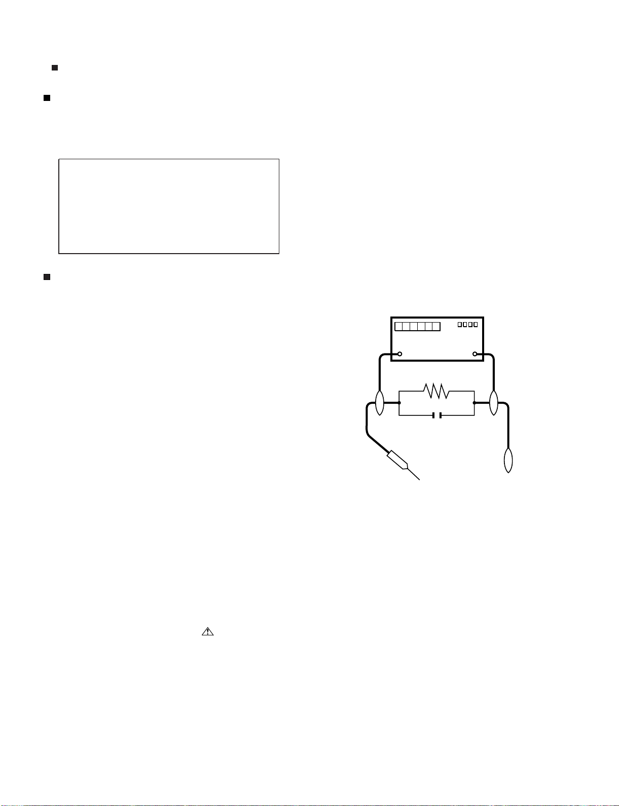
• Use an AC voltmeter having with 5000 ohm per volt, or higher, sensitivity or measure the AC voltage drop across the resistor.
• Connect the resistor connection to all exposed metal parts having a
return to the chassis (antenna, metal cabinet, screw heads, knobs
and control shafts, escutcheon, etc.) and measure the AC voltage
drop across the resistor.
All checks must be repeated with the AC cord plug connection
reversed. (If necessary, a nonpolarized adaptor plug must be used
only for the purpose of completing these checks.)
Any reading of 1.05 V peak (this corresponds to 0.7 mA peak AC.)
or more is excessive and indicates a potential shock hazard which
must be corrected before returning the monitor to the owner.
F7102 (250V 1A)
DVM
AC SCALE
BEFORE RETURNING THE RECEIVER
(Fire & Shock Hazard)
Before returning the receiver to the user, perform the following
safety checks:
3. Inspect all lead dress to make certain that leads are not pinched,
and check that hardware is not lodged between the chassis and
other metal parts in the receiver.
4. Inspect all protective devices such as non-metallic control knobs,
insulation materials, cabinet backs, adjustment and compartment
covers or shields, isolation resistor-capacitor networks, mechanical
insulators, etc.
5. To be sure that no shock hazard exists, check for leakage current in
the following manner.
• Plug the AC cord directly into a 220~240 volt AC outlet.
• Using two clip leads, connect a 1.5k ohm, 10 watt resistor paralleled by a 0.15µF capacitor in series with all exposed metal cabinet
parts and a known earth ground, such as electrical conduit or electrical ground connected to an earth ground.
///////////////////////////////////////////////////////////////////////////////////////////////////////////////////////////////////////////////////////////////////////////////////////////////////////////////////////////////////////////
TO EXPOSED
METAL PARTS
1.5k ohm
10W
0.15µF
TEST PROBE
CONNECT TO
KNOWN EARTH
GROUND
SAFETY NOTICE
Many electrical and mechanical parts in LCD color television have
special safety-related characteristics.
These characteristics are often not evident from visual inspection, nor
can protection afforded by them be necessarily increased by using
replacement components rated for higher voltage, wattage, etc.
Replacement parts which have these special safety characteristics are
identified in this manual; electrical components having such features
are identified by “ ” and shaded areas in the Replacement Parts
List and Schematic Diagrams.
///////////////////////////////////////////////////////////////////////////////////////////////////////////////////////////////////////////////////////////////////////////////////////////////////////////////////////////////////////////
For continued protection, replacement parts must be identical to those
used in the original circuit.
The use of a substitute replacement parts which do not have the same
safety characteristics as the factory recommended replacement parts
shown in this service manual, may create shock, fire or other hazards.
i
Page 3
LC32D44E/S/RU-BK/GY (1st Eddition)
PRECAUTIONS A PRENDRE LORS DE LA REPARATION
Ne peut effectuer la réparation qu' un technicien spécialisé qui s'est parfaitement accoutumé à toute vérification de sécurité et aux
conseils suivants.
•
AVERTISSEMENT
1.
N'entreprendre aucune modification de tout circuit. C'est dangereux.
2.
Débrancher le récepteur avant toute réparation.
PRECAUTION: POUR LA PROTECTION CONTINUE CONTRE LES RISQUES D'INCENDIE,
REMPLACER LE FUSIBLE
F7101, F7103 (250V 3.15A)
F7102 (250V 1A)
VERIFICATIONS CONTRE L'INCEN-DIE ET LE
CHOC ELECTRIQUE
Avant de rendre le récepteur à l'utilisateur, effectuer les vérifications suivantes.
Inspecter tous les faisceaux de câbles pour s'assurer que les fils
3.
ne soient pas pincés ou qu'un outil ne soit pas placé entre le châssis et les autres pièces métalliques du récepteur.
4.
Inspecter tous les dispositifs de protection comme les boutons de
commande non-métalliques, les isolants, le dos du coffret, les couvercles ou blindages de réglage et de compartiment, les réseaux
de résistancecapacité, les isolateurs mécaniques, etc.
5.
S'assurer qu'il n'y ait pas de danger d'électrocution en vérifiant la
fuite de courant, de la facon suivante:
•
Brancher le cordon d'alimentation directem-ent à une prise de courant de 120V. (Ne pas utiliser de transformateur d'isolation pour
cet essai).
A l'aide de deux fils à pinces, brancher une résistance de 1.5 kΩ
10 watts en parallèle avec un condensateur de 0.15µF en série
avec toutes les pièces métalliques exposées du coffret et une terre
connue comme une conduite électrique ou une prise de terre
branchée à la terre.
•
Utiliser un voltmètre CA d'une sensibilité d'au moins 5000Ω/V pour
mesurer la chute de tension en travers de la résistance.
•
Toucher avec la sonde d'essai les pièces métalliques exposées qui
présentent une voie de retour au châssis (antenne, coffret métallique, tête des vis, arbres de commande et des boutons, écusson,
etc.) et mesurer la chute de tension CA en-travers de la résistance.
Toutes les vérifications doivent être refaites après avoir inversé la
fiche du cordon d'alimentation. (Si nécessaire, une prise
d'adpatation non polarisée peut être utilisée dans le but de terminer ces vérifications.)
La tension de pointe mesurèe ne doit pas dépasser 0.75V (correspondante au courant CA de pointe de 0.5mA).
Dans le cas contraire, il y a une possibilité de choc électrique qui
doit être supprimée avant de rendre le récepteur au client.
DVM
ECHELLE CA
1.5k ohm
10W
µ
F
0.15
SONDE D'ESSAI
AUX PIECES
METALLIQUES
EXPOSEES
/////////////////////////////////////////////////////////////////////////////////////////////////////////////////////////////////////////////////////////////////////////////////////////////////////////////////////////////////////////////
BRANCHER A UNE
TERRE CONNUE
AVIS POUR LA SECURITE
De nombreuses pièces, électriques et mécaniques, dans les téléviseur ACL présentent des caractéristiques spéciales relatives à la sécurité, qui ne sont souvent pas évidentes à vue. Le degré de protection ne peut pas être nécessairement augmentée en utilisant des
pièces de remplacement étalonnées pour haute tension, puissance,
etc.
Les pièces de remplacement qui présentent ces caractéristiques sont
identifiées dans ce manuel; les pièces électriques qui présentent ces
particularités sont identifiées par la marque " " et hachurées dans la
liste des pièces de remplacement et les diagrammes schématiques.
/////////////////////////////////////////////////////////////////////////////////////////////////////////////////////////////////////////////////////////////////////////////////////////////////////////////////////////////////////////////
Pour assurer la protection, ces pièces doivent être identiques à celles
utilisées dans le circuit d'origine. L'utilisation de pièces qui n'ont pas
les mêmes caractéristiques que les pièces recommandées par l'usine,
indiquées dans ce manuel, peut provoquer des électrocutions, incendies, radiations X ou autres accidents.
ii
Page 4

LC32D44E/S/RU-BK/GY (1st Eddition)
PRECAUTIONS FOR USING LEAD-FREE SOLDER
Employing lead-free solder
• “PWBs” of this model employs lead-free solder. The LF symbol indicates lead-free solder, and is attached on the PWBs and service manuals. The
alphabetical character following LF shows the type of lead-free solder.
Example:
Indicates lead-free solder of tin, silver and copper. Indicates lead-free solder of tin, silver and copper.
Using lead-free wire solder
• When fixing the PWB soldered with the lead-free solder, apply lead-free wire solder. Repairing with conventional lead wire solder may cause damage or accident due to cracks.
As the melting point of lead-free solder (Sn-Ag-Cu) is higher than the lead wire solder by 40 °C, we recommend you to use a dedicated soldering
bit, if you are not familiar with how to obtain lead-free wire solder or soldering bit, contact our service station or service branch in your area.
Soldering
• As the melting point of lead-free solder (Sn-Ag-Cu) is about 220 °C which is higher than the conventional lead solder by 40 °C, and as it has poor
solder wettability, you may be apt to keep the soldering bit in contact with the PWB for extended period of time. However, Since the land may be
peeled off or the maximum heat-resistance temperature of parts may be exceeded, remove the bit from the PWB as soon as you confirm the
steady soldering condition.
Lead-free solder contains more tin, and the end of the soldering bit may be easily corroded. Make sure to turn on and off the power of the bit as
required.
If a different type of solder stays on the tip of the soldering bit, it is alloyed with lead-free solder. Clean the bit after every use of it.
When the tip of the soldering bit is blackened during use, file it with steel wool or fine sandpaper.
• Be careful when replacing parts with polarity indication on the PWB silk.
Lead-free wire solder for servicing
PARTS CODE
ZHNDAi123250E BL J φ0.3mm 250g (1roll)
ZHNDAi126500E BK J φ0.6mm 500g (1roll)
ZHNDAi12801KE BM J φ1.0mm 1kg (1roll)
PRICE
RANK
PART
DELIVERY
DESCRIPTION
iii
Page 5
LC32D44E-BK
CHAPTER 1. SPECIFICATIONS
[1] SPECIFICATIONS
LC32D44E/S/RU-BK/GY (1st Eddition)
Service Manual
Item
LCD panel
Resolution
Video Colour System PAL/SECAM/NTSC 3.58/NTSC 4.43/PAL 60
TV
Function
Brightness 450 cd/m2
Viewing angles H : 176° V : 176°
Audio amplifier
Speaker
Terminals Antenna
OSD language English/German/French/Italian/Spanish/Dutch/Swedish/Portuguese/Finnish/Turkish/Greek/
Power Requirement AC 220-240 V,50 Hz
Power Consumption 120 W (0.9 W Standby) (Method IEC60107)
Weight 11.0 kg (Display only), 13.0 kg (Display with stand)
Operating temperature
TV-Standard Analogue CCIR (B/G, I, D/K, L, L’)
Digital DVB-T (2K/8K OFDM)
Receiving
Channel
TV-Tuning System Auto Preset 99 ch, Auto Label, Auto Sort
STEREO/BILINGUAL NICAM/A2
RS-232C 9 pin mini D-sub
EXT 1 SCART (AV input, Y/C input, RGB input, TV output)
EXT 2 SCART (AV input/output, Y/C input, RGB input, AV Link)
EXT 3 S-VIDEO (Y/C input), RCA pin (AV input)
EXT 4 Ø 3.5 mm jack (Audio input), 15 pin mini D-sub (PC)
EXT 5 Audio in, Component in
EXT 6 HDMI, Ø 3.5 mm jack (Audio input)
EXT 7 HDMI
C. I. (Common Interface) EN50221, R206001
OUTPUT RCA pin (Audio)
Headphones Ø 3.5 mm jack (Audio output)
VHF/UHF E2-E69ch, F2-F10ch, I21-I69ch, IR A-IR Jch, (Digital: E5-E69ch)
CATV Hyper-band, S1-S41ch
32" LCD COLOUR TV
32" Advanced Super View & BLACK TFT LCD
1,049,088 pixels (1,366 x 768)
10W x 2
(100mmx35mm)x2
UHF/VHF 75Ω Din type (Analogue & Digital)
Russian/Polish
0°Cto+40°C
• As a part of policy of continuous improvement, SHARP reserves the right to make design and specification changes for
product improvement without prior notice. The performance specification figures indicated are nominal values of production
units. There may be some deviations from these values in individual units.
NOTE
• Refer to inside back cover for dimensional drawings.
Optional accessory
The listed optional accessories are available for the
LCD colour TV. Please purchase them at your nearest
shop.
• Additional optional accessories may be available in near
future. When purchasing, please read the newest catalogue
for compatibility and check the availability.
Wall mount bracket
(LC-32D44E, LC-32D44S)
1 – 1
Part name Part number
AN-37AG5
Page 6

LC32D44E/S/RU-BK/GY (1st Eddition)
[2] OPERATION MANUAL
Remote control unit
1 (Standby/On)
Enter standby mode or turn on the
power.
2AVMODE
Select a video setting.
30–9
Set the channel in TV and DTV mode.
Set the page in Teletext mode.
When Sweden is selected in the
country setting from the Initial
auto installation, DTV channels
are 4-digit. When another
country is selected, DTV channels
are 3-digit.
4 (Flashback)
Press to return to the previous image
in normal viewing mode. (Will not work
while operating in EPG/ESG screen.)
5 (WIDE MODE)
Select the wide mode.
6 (Sound mode)
Select the sound multiplex mode.
(See below.)
7 EPG
DTV: To display EPG (Electronic
Programme Guide) screen.
8 ESG
DTV: To display ESG (Electronic Service
Guide) screen.
9 (Teletext)
Select the TELETEXT mode. (All TV
image, DTV/DATA image, all TEXT
image, TV/TEXT image)
DTV: Select DTV data broadcasting and
TELETEXT.
10 / / / (Cursor)
Select a desired item on the setting
screen.
11 END
Exit the menu screen.
12 (Reveal hidden Teletext)
13 (Freeze/Hold)
Using on the remote control unit
DTV mode:
Press to open the multi audio screen.
Analogue TV mode:
Each time you press , the mode switches as illustrated in the following
tables.
NICAM TV broadcasts selection
Signal Selectable items
Stereo
Bilingual
Monaural
NOTE
• When no signal is input, the sound mode will display “MONO”.
NICAM STEREO, MONO
NICAM CH A, NICAM CH B,
NICAM CH AB, MONO
NICAM MONO, MONO
1
2
3
4
5
6
7
8
9
10
11
12
13
A2 TV broadcasts selection
Signal Selectable items
Stereo
Bilingual
Monaural
STEREO, MONO
CH A, CH B, CH AB
MONO
14 SURROUND
14
15
16
17
18
19
20
21
22
23
24
25
26
27
28
29
Switch the surround effects on and off.
15 RADIO
DTV: Switch between RADIO and DTV
mode.
16 (Mute)
Switchthesoundonandoff.
17 DTV
Press to access DTV mode while
watching other input sources, and vice
versa.
(This button will not work if you were
watching DTV immediately before
turning off the TV. In this case first select
any other input source except DTV
using the button.)
18 (+/-) (Volume)
(+) Increase the volume.
(-) Decrease the volume.
19 P ( / )
TV/DTV: Select the channel.
External: Switch to TV or DTV input
mode.
eletext: Move to the next/previous
20 (INPUT SOURCE)
Select an input source.
(TV, DTV, EXT1, EXT2, EXT3, EXT4,
EXT5, EXT6, EXT7)
21 SLEEP
Set the sleep timer on (in units of 30
min. up to max. 2 hr. 30 min) and off.
22 (Display information)
23 DTV MENU
DTV: Display DTV Menu screen.
24 MENU
Display the MENU screen.
25 OK
Execute a command within the menu
screen.
Display the programme list. (Except
external input.)
26 RETURN
Return to the previous menu screen.
27 (Subpage)
28 (Subtitle for Teletext)
TV/External: To turn the subtitles on and
off.
DTV: Display the subtitle selection
screen.
29 Colour (Red/Green/Yellow/Blue)
TELETEXT: Select a page.
DTV: The coloured buttons are used to
select correspondingly to the coloured
items in the menu screen.
1 – 2
Page 7

TV (Front view)
LC32D44E/S/RU-BK/GY (1st Eddition)
TV (Rear view)
-/+) (Volume buttons)
(
(Programme [channel] buttons)
1
Remote control sensor
P (/)
(Standby/On) indicator
(Power button)
MENU button
(Input button)
10
6
7
8
2
9
4 5
3
11
12
1 RS-232C terminal
2 EXT 4 (ANALOGUE RGB/AUDIO)
terminals
3 EXT 5 (COMPONENT) terminals
4 EXT 1 (RGB) terminal
5 EXT 2 (RGB) terminal
NOTE
• Only if you use an active terrestrial antenna, select “On (5V)” under “Supply Voltage”.
6 Antenna input terminal
(DVB-T 5V=/80 mA)
7 OUTPUT (AUDIO) terminals
8 EXT 6 (HDMI/AUDIO) terminals
9 EXT 7 (HDMI) terminal
10 COMMON INTERFACE slot
11 EXT 3 terminals
12 Headphone jack
13 AC INPUT terminal
1 – 3
13
Page 8

LC32D44E/S/RU-BK/GY (1st Eddition)
Appendix
Troubleshooting
Problem Possible Solution
• No power.
• Unit cannot be operated. • External influences such as lightning, static electricity, etc., may cause improper
• Remote control unit does not
operate.
• Picture is cut off. • Is the image position correct?
• Strange colour, light colour, or
dark, or colour misalignment.
• Power is suddenly turned off. • The unit’s internal temperature has increased.
• No picture. • Is connection to other components correct?
• No sound. • Is the volume too low?
• The DTV menu screen is displayed
in monochrome and hard to select
the item.
• The TV sometimes makes a
cracking sound.
• Check if you pressed on the remote control unit.
If the indicator on the TV lights up red, press .
• Is the AC cord disconnected?
• Check if you pressed on the TV.
operation. In this case, operate the unit after first turning the power off, or
unplugging the AC cord and re-plugging it in after 1 or 2 minutes.
• Are batteries inserted with polarity (+, -) aligned?
• Are batteries worn out? (Replace with new batteries.)
• Are you using it under strong or fluorescent lighting?
• Is a fluorescent light illuminated to remote control sensor?
• Are screen mode adjustments (4:3 Mode/WSS) such as picture size made
correctly?
• Adjust the picture tone.
• Is the room too bright? The picture may look dark in a room that is too bright.
• Check the colour system setting.
• Check the HDMI Setup setting.
Remove any objects blocking vent or clean.
• Check the power control setting.
• Is sleep timer set? Press SLEEP on the remote control unit until it sets to Off.
• Is input signal type selected correctly after connection?
• Is the correct input source selected?
• Is non-compatible signal being input?
• Is picture adjustment correct?
• Is the antenna connected properly?
• Is “On” selected in “Audio Only”?
• Make sure that headphones are not connected.
• Check if you pressed on the remote control unit.
• Check if “Monochrome” is set to “On”. If so, set it to “Off”.
• This is not a malfunction. This happens when the cabinet slightly expands and
contracts according to change in temperature. This does not affect the TV’s
performance.
Cautions regarding use in high and low temperature environments
• When the unit is used in a low temperature space (e.g. room, office), the picture may leave trails or appear slightly
delayed. This is not a malfunction, and the unit will recover when the temperature returns to normal.
• Do not leave the unit in a hot or cold location. Also, do not leave the unit in a location exposed to direct sunlight or near a
heater, as this may cause the cabinet to deform and the LCD panel to malfunction.
Storage temperature: -20°C to +60°C.
IMPORTANT NOTE ON RESETTING THE PIN
We suggest that you remove the following instruction from the operation manual to prevent children from
reading it. As this operation manual is multilingual, we also suggest the same with each language. Keep it in a
safe space for future reference.
1 – 4
Page 9

[3] DIMENSIONS
LC32D44E/S/RU-BK/GY (1st Eddition)
575.0
575,0
523.0
523,0
52.0
52,0
699.2
699,2
776.0
776,0
402.0
402,0
200.0
200,0
393.8
393,8
332.0
332,0
73.9
73,9
94.5
94,5
230.0
230,0
200.0
200,0
110.0
110,0
1 – 5
Page 10

LC32D44E/S/RU-BK/GY (1st Eddition)
LC32D44E-BK
CHAPTER 2. REMOVING OF MAJOR PARTS
Service Manual
[1] REMOVING OF MAJOR PARTS
1. Remove the 4 lock screws and detach the Stand.
2. Remove the 3 lock screws , 6 lock screws , 2 lock screw and detach the Rear Cabinet.
1
2
3
4
Rear Cabinet
2
Front Cabinet
3
4
1
Stand
2 – 1
Page 11

LC32D44E/S/RU-BK/GY (1st Eddition)
3. Remove the 3 lock screws , 2 lock screws , 1 lock screws and detach the Main Shield.
4. Disconnect all the connectors from all the PWBs.
5. Remove the KEY Unit Ass'y .
Operation Button
5A 5B 6
7
6
5B
7
5A
Main Shield
KEY Unit
[KM]
[KM]
[FPC]
[LB]
[PD]
SP-R
[RA]
[LB]
[PD]
[SP]
SP-L
2 – 2
Page 12

LC32D44E/S/RU-BK/GY (1st Eddition)
6. Remove the Speaker (L) , (R) .
7. Remove the 4 lock screws and detach the POWER/INVERTER Unit.
8. Remove the 2 lock screws , and detach the MAIN Unit.
9. Remove the 2 lock screws and detach the MINI AV Unit.
8 9
10
11
12
MINI AV Cover
11
12
Main Unit
MINI AV Unit
10
Power/Inverter Unit
Speaker(R) Speaker(L)
98
2 – 3
Page 13

LC32D44E/S/RU-BK/GY (1st Eddition)
10.Remove the 1 lock screw and detach the Bottom Cover.
11.Remove the 4 lock screws and detach the Stand Fix Angle.
12.Remove the R/C, LED Unit .
13
14
15
15
R/C,LED Unit
14
Stand Fix Angle
Bottom Cover
13
2 – 4
Page 14

LC32D44E/S/RU-BK/GY (1st Eddition)
13.Remove the 6 lock screws and detach the LCD Panel Module.
14.Remove the 2 lock screws and detach the LCD Fix Angle-A.
15.Remove the 2 lock screws and detach the LCD Fix Angle-B.
16.Remove the 8 lock screws and detach the Panel Fix Angle.
16
18
16
17
18
19
LCD Fix Angle-B
16
19
16
19
16
LCD Fix Angle-A
17
LCD Fix Angle-B
18
17
Panel Fix Angle
LCD Fix Angle-A
16
16
2 – 5
Page 15

LC32D44E/S/RU-BK/GY (1st Eddition)
LC32D44E-BK
CHAPTER 3. ADJUSTMENT
Service Manual
[1] After replacement of any PWB and/or IC for repair, note the following.
When replacing the following units, be sure to prepare the new units loaded with updated software.
MAIN-UNIT: DUNTKE449FM02
• Note that an IC into which ROM data is written is available for MAIN-UNIT servicing (see below)
IC1902 RH-iXC448WJZZS EDID (HDMI)
IC1922 RH-iXC447WJZZS EDID (HDMI)
IC2321 RH-iXC206WJQZS EDID (PC)
IC8101 RH-iXC639WJZZS EEPROM
[2] SOFTWARE UPDATING
There are 2 methods to update software in the VCTp: I2C method, RS-232C HyperTerminal and RS-232C Tera Term method.
• RS-232C method is allowed when the TV is working properly and the action should be only software upgrade.
1. RS-232C Method Description (HyperTerminal).
The hardware tools requirement are:
1. A Modem-null (Cross type) DB9 female to DB9 female cable.
2. Make the connections as indicated in the figure:
Computer TV set
TV Set
RS-232C
IOIOI
Before using RS-232C updating method is necessary to configure a Terminal PC software. HyperTerminal has been selected as a Terminal software because it’s include in all Windows versions as an accessory, and you can find it inside “Accessories\Communications” folder. For this reason, please follow carefully the next steps:
1) First time HyperTerminal is used, it’s necessary to configure some settings. Follows next action to configure two connection: low speed
(9600bps) and high speed (115200bps).
2) Create a New Connection file with name “P55_9600bps”.
3) Select a free COM port and select the Port Settings properties as follows:
3 – 1
Page 16

LC32D44E/S/RU-BK/GY (1st Eddition)
4) Click on “File\Properties” menu for selecting the General and ASCII properties as follows:
5) Select “New Connection” in the File Menu.
6) Answer “Yes” to close current connection and “Yes” to save session “P55_9600bps”.
7) Create a new connection with the name “P55_115200bps”.
8) Select a the same COM port used in item 2 and select the Port Settings properties as follows:
9) Select the same General and ASCII properties as item 3.
10)Close HyperTerminal session, answering “Yes” to close current connection and “Yes” to save session “P55_115200bps”.
To start updating session, click over “P55_9600bps” icon that you can find in the “START\All programs\Accessories\ Communications\HyperTerminal\HyperTerminal” folder and follow next procedure:
3 – 2
Page 17
LC32D44E/S/RU-BK/GY (1st Eddition)
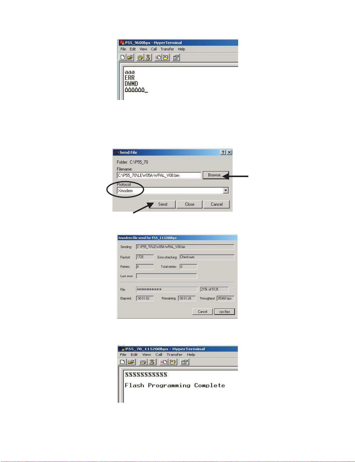
1) Check the connection between TV set and PC, sending a wrong command, as for example: “aaa”. TV set returns an “ERR” label as an syntaxis
ERROR (Not correct order or sequence).
2) Send the command “DWMD” to enter TV set in Download Mode. The TV set answer sending same symbol continuosly. If this symbol character
doesn’t appear, please don’t worry and pass to next step.
3) Close this connection and open “P55_115200bps” connection clicking over the “P55_115200bps” that you can find in “START\All programs\Accessories\ Communications\HyperTerminal\HyperTerminal” folder.
4) Using “Transfer\Send file...” menu, select desired file (.bin format) and the transmission protocol (Xmodem) as show below.
5) After press “Send” button the updating process starts as follows:
6) When flash update process finishes, the “Flash Programming Complete” label appears in the screen, the device automatically go to switch off,
and in a few seconds go to switch on again.
VERY IMPORTANT NOTE:
During the updating time, please don’t use the PC for other purpouses, in order to abolish communication problems between TV set and
PC. If TV set was not updated properly, the TV won’t have the software to startup again, and you must follow the “I2C method” to update
another time the TV set.
3 – 3
Page 18

LC32D44E/S/RU-BK/GY (1st Eddition)
2. RS-232C Method Description (Tera Term)
The hardware tools requirement are:
1. A Modem-null (Cross type) DB9 female to DB9 female cable.
2. Make the connections as indicated in the figure:
Computer TV set
TV Set
Software requirements:
To upgrade VCTp software from RS-232C external connector is necessary to use a Tera Term (Pro) free software.
The URL of Tera Term home page is:
http://hp.vector.co.jp/authors/VA002416/teraterm.html
(The address may be changed in future)
Tera Term (Pro) supported operating systems:
MS-Windows 95 or upper
MS-Windows NT 3.5 and 4.0 or upper
Note.- For Windows 3.1 use Tera Term version 1.X.
Copy all the distribution files to an empty floppy disk or temporary directory (for example C:\ TEMP).
Run SETUP.EXE and follow the instruction given by it.
After the installation, the distribution? les are no longer needed, you can delete them or may keep them in the floppy disk.
Ho w to us e Tera Te rm Pro :
When the Tera Term (Pro) program is used, it’s necessary to shape some settings. Follows next action to configure the connection:
RS-232C
IOIOI
3 – 4
Page 19

1) Select: Serial→COM X→ O.K.
2) Select: Ter minal
LC32D44E/S/RU-BK/GY (1st Eddition)
3) Choose the same options as the above picture.
3 – 5
Page 20

LC32D44E/S/RU-BK/GY (1st Eddition)
4) Select: Setup → Serial port → O.K. Appear the follow screen:
5) Select follows settings:
Serial port to use: COM x
Baud rate: 9600
Data: 8 bits
Parity: none
Stop: 1 bit
Flow control: none
Enter O.K.
6) Check the connection between TV set and PC, sending a wrong command, as for example: “aaa”. TV set returns an “err” label as an syntaxes
ERROR (Not correct order or sequence).
Send a “DWMD” (capital letters) command to enter TV set in Download Mode.
Change a baud rate to 115200.
Select: Setup → Baud rate → 115200 → O.K.
3 – 6
Page 21
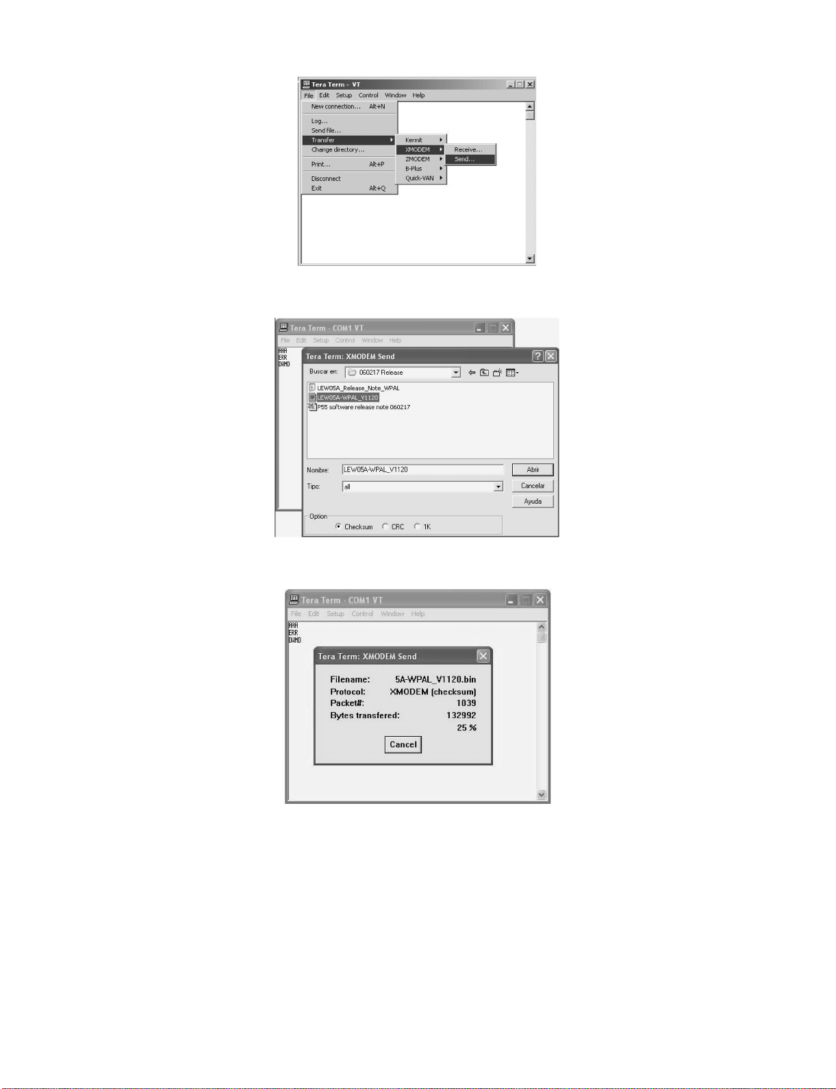
7) Select: File → Transfer → XMODEM → Sent
8) Choose the file for upgrade and click “Open”.
LC32D44E/S/RU-BK/GY (1st Eddition)
9) After select “Open” the upgrade process starts as follows:
3 – 7
Page 22

LC32D44E/S/RU-BK/GY (1st Eddition)
10)When flash update process finishes, the “Flash programming complete” label appear in the screen, the device automatically go to switch off, and
in a few seconds go to switch on again.
VERY IMPORTANT NOTE:
During the updating time, please don’t use the PC for other purposes, in order to abolish communication problems between TV set and PC.
If TV set was not updated properly, the TV won’t have the software to startup again, and you must follow the “I2C method”
another time the TV set.
3. How to update the Digital Board Software.
There are 2 methods to update the Digital Board Software on Flash Memory (IC4251) throught the Digital Processor (IC4001).
• RS-232 Method (From PC trough RS-232C COM port).
• PCMCIA CARD (Compact Flash Memory) Method.
NOTE: The PCMCIA method is only compatible with those PCs running XP Windows Version.
to update
3.1. Jig RS-232 Method Description
• Hardware requirements:
1. A modem null (Cross type) DB9 female to DB9 female cable.
2. Make the connections as in the below figure.
Computer
RS-232C serial control cable
(cross type, commercially available)
TV Set
(CI Terminal)
TV Set
Jig
~
~
RS-232C
IOIOI
• Software requirements:
1. “Winupload” application software on PC.
3 – 8
Page 23

• How to setup the “Winupload” software for the first time:
1. Start “Winupload”. It will appear the following picture.
2. Select the most suitable RS232 Serial Port from “Port Setting” - “Process” Menu.
LC32D44E/S/RU-BK/GY (1st Eddition)
3. Select the following settings from “Port Settings” Menu.
Bits Per Second: 115200
Parity: None
Data bits: 8
Stop bits: 1
Hardware Flow Control: OFF
• Procedure for updating the TV set.
1. Switch off the TV set to be updated, in DTV mode.
2. Start “Winupload”. It will appear the following picture on PC.
3 – 9
Page 24

LC32D44E/S/RU-BK/GY (1st Eddition)
3. Establish connection on Winupload Software.
4. Select “Upload URT file”
5. Select and open the “.urt” data file from data directory
NOTE: Consider the version shown below just an example, may be is not the latest one, and could be different depending on the TV set destination
(market/Country) or model.
6. Switch On the TV Set (previously in DTV Mode). The Uploading Process starts automatically.
3 – 10
Page 25

LC32D44E/S/RU-BK/GY (1st Eddition)
While the TV set is uploading the software, the following information is shown on the TV set screen.
Then, data transfer from PC to TV set finishes when the “Upload progress completed” label appears in the “Winupload” screen. Now, the TV set made
some additional verification (Items #2 to #7). When the full uploading process is finished, in the “Winupload” window appears the label “Preparing to
start application” for a new TV Set, and just now, in the TV screen of the updated set, appears a congratulations label (Item #8).
NOTE: Do not turn off the TV set while the software updating was in progress.
7. Unplug the AC cord.
8. Disconnect the Jig from TV Set.
• Software Version verification procedure.
1. Connect the AC cord and Switch On the TV Set.
2. Select DTV Menu on TV Set. The following On Screen Display will appear.
3. Select “Version”. The updated version can be verified.
NOTE: Consider the version shown above just as example, may be is not the latest one, and could be different depending on the TV set destination
(market/Country) or model.
3 – 11
Page 26

LC32D44E/S/RU-BK/GY (1st Eddition)
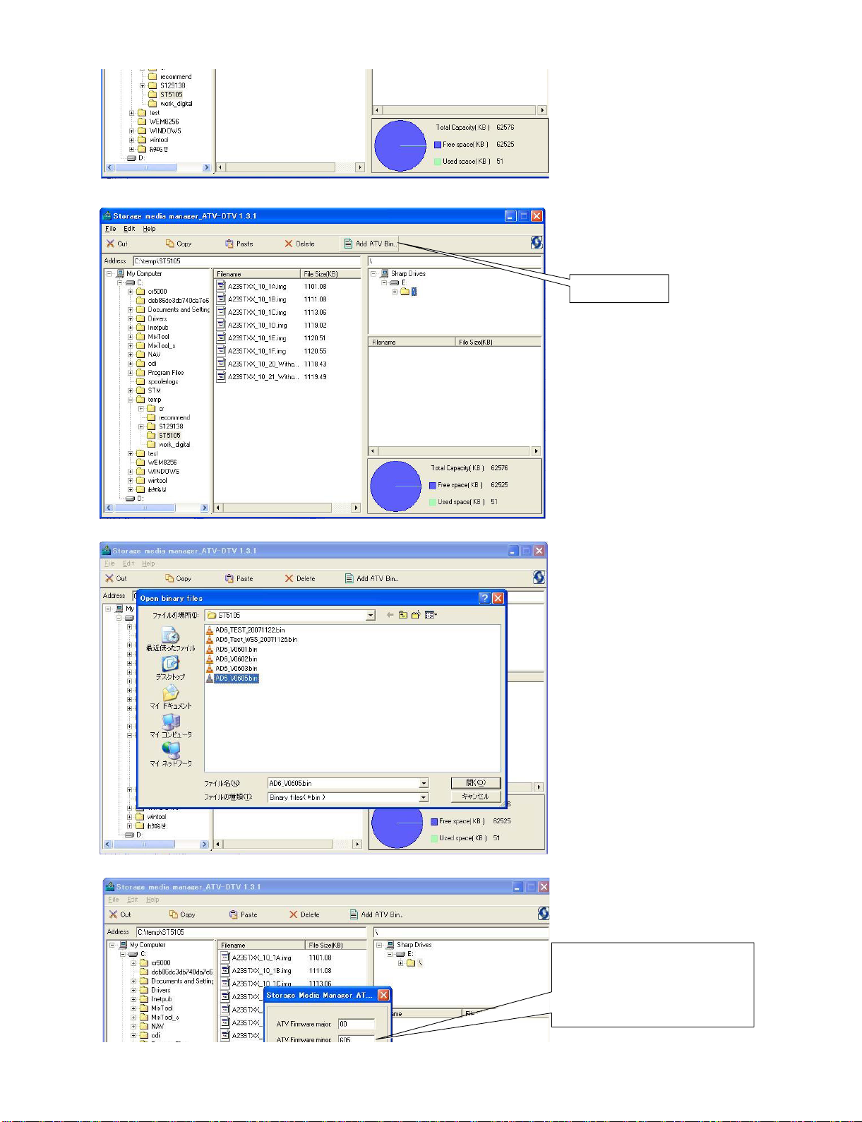
4. Software Version Upgrade Using Card
1. Write the software (ATV and DTV) on the PCMCIA CARD by following the procedure described in the separate document, “How to write software
(ATV and DTV) to PCMCIA CARD”.
(* In the document, both ATV and DTV are written; you may write either of them.)
(You can equally use any version after “Storage Media Manager Version 1.3.1”.)
2. Turn off the power.
(* You can select either of the mode ATV or DTV. In this document, ATV is selected.)
3. Insert the PCMCIA CARD with the upper side facing up into the card slot.
(* Do not insert the card with the upper side facing down.)
4. Turn on the power. After a short time, the message, “SYSTEM SOFTWARE UPDATE IN PROGRESS. ...) appears and the software upgrade
starts.
If the ATV software upgrade is necessary, the step proceeds to (5); if unnecessary, the DTV software upgrade starts and the step proceeds to (7).
5. If the ATV software upgrade is necessary, the following display appears and the upgrade starts.
When the status bar reaches 100 %, the ATV upgrade is complete. Then the system restarts from the ATV mode. The step proceeds to (6).
3 – 12
Page 27

LC32D44E/S/RU-BK/GY (1st Eddition)
6. The message, “SYSTEM SOFTWARE UPDATE IN PROGRESS. ...” appears again and the DTV software upgrade starts. Then the step proceeds
to (7).
7. After a short time, the message, “Congratulations! ...” appears. The upgrade is complete.
(Note: You cannot downgrade the ATV software but can downgrade the DTV software.)
3 – 13
Page 28

LC32D44E/S/RU-BK/GY (1st Eddition)
㪟㫆㫎㩷㫋㫆㩷㫎㫉㫀㫋㪼㩷㫊㫆㪽㫋㫎㪸㫉㪼㩿㪘㪫㪭㩷㪸㫅㪻㩷㪛㪫㪭㪀㩷㫋㫆㩷㪧㪚㪤㪚㪠㪘㩷㪚㪘㪩㪛
㪈㪅㪮㪿㪼㫅㩷㫐㫆㫌㩷㫎㫉㫀㫋㪼㩷㫊㪆㫎㩷㪃㩷㫐㫆㫌㩷㫊㪿㫆㫌㫃㪻㩷㫌㫊㪼㩷 㩹㪪㫋㫆㫉㪸㪾㪼㪤㪼㪻㫀㪸㪤㪸
㪉㪅㪪㫋㪸㫉㫋㩷㩹㪪㫋㫆㫉㪸㪾㪼㪤㪼㪻㫀㪸㪤㪸㫅㪸㪾㪼㫉㪶㪘㪫㪭㪄㪛㪫㪭㩷㪈㪅㪊㪅㪈㪅㪼㫏㪼㩹㪅㩿㪛㫀㫊㫇㫃㪸㫐㪼㪻㩷㪸㫊㩷㪽㫆㫃㫃㫆㫎㫊㪅㪀
㫅㪸㪾㪼㫉㪶㪘㪫㪭㪄㪛㪫㪭㩷㪈㪅㪊㪅㪈㪅㪼㫏㪼㩹
㪇㪊㪛㪼㪺㪶㪉㪇㪇㪎
㪮㫉㫀㫋㪼㫅㩷㪹㫐㩷㪢㪼㫅㫋㪸㫉㫆㩷㪪㪼㫐㪸㫄㪸㩿㪪㪟㪘㪩㪧㩷㪡㪸㫇㪸㫅㪀㩷
㪸㫋㩷㫋㪿㪼㩷㪛㫉㫀㫍㪼
㪊㪅㪝㫆㫉㫄
㪋㪅㪚㪿㫆㫆㫊㪼㩷㪽㫆㫃㪻㪼㫉
㪚㫃㫀㪺㫂㩷㫋㪿㪼㩷㫉㫀㪾㪿㫋㩷㪹㫌㫋㫋㫆㫅㩷㪸㫋㩷㪜㪑㩷㪻㫉㫀㫍㪼㩿㪫㪿㪼㩷㪻㫉㫀㫍㪼㩷㫋㪿㪸㫋㩷㫋㪿㪼
㫄㪼㪻㫀㪸㩷㪽㫆㫉㩷㪧㪚㪤㪚㪠㪘㩷㫌㫇㪻㪸㫋㪼㩷䌩䌳㩷䌩䌮䌳䌥䌲䌴䌥䌤㩷㫀㫅㪅㪀㪅
㪘㫅㪻㩷㪃㩷㪺㪿㫆㫆㫊㪼㩷㩹㪝㫆㫉㫄㪸㫋㩷㪛㫉㫀㫍㪼㩹㪅
3 – 14
㪚㪿㫆㫆㫊㪼㩷㫋㪿㫀㫊㩷㪽㫆㫃㪻㪼㫉㪅
Page 29
㪌㪅㪮㫉㫀㫋㪼㩷㪘㪫㪭㩷㫊㫆㪽㫋㫎㪸㫉㪼
㪌㪄㪈㪀㪚㪿㫆㫆㫊㪼㩷㩹㪘㪻㪻㩷㪘㪫㪭㩷㪙㫀㫅㩷㪅㪅㪅㩹
LC32D44E/S/RU-BK/GY (1st Eddition)
㪚㪿㫆㫆㫊㪼㩷㩹㪘㪻㪻㩷㪘㪫㪭
㪙㫀㫅㪅㪅㪅㩹
㪌㪄㪉㪀㪪㪼㫃㪼㪺㫋㩷㫋㪿㪼㩷㪘㪫㪭㩷㫊㫆㪽㫋㫎㪸㫉㪼㪅㩿㪪㫆㫉㫉㫐㩷㪽㫆㫉㩷㪻㫀㫊㫇㫃㪸㫐㪼㪻㩷㪹㫐㩷㪡
㪌㪄㪊㪀㪠㫅㫇㫌㫋㩷㩹㫄㪸㫁㫆㫉㩷㪺㫆㪻㪼㩹㩷㪸㫅㪻㩷㩹㫄㫀㫅㫆㫉㩷㪺㫆㪻㪼㩹㪅
㪸㫇㪸㫅㪼㫊㪼㪅㪀
3 – 15
㪠㫅㫇㫌㫋㩷㫋㪿㪼㩷㩹㫄㪸㫁㫆㫉㩷㪺㫆㪻㪼㩹㩷㪸㫅㪻㩷㩹㫄㫀㫅㫆㫉㩹㩷㪺㫆㪻㪼㪅
㪄㪄㪜㫏㪅㪄㪄㪄
㪮㪿㪼㫅㩷㫐㫆㫌㩷㫎㫆㫌㫃㪻㩷㫃㫀㫂㪼㩷㫋㫆㩷㫎㫉㫀㫋㪼㩷㫊㪆㫎㩷㫍㪼㫉㫊㫀㫆㫅㩷㩹㪇㪅㪍㪇㪌㩹㩷㪃
㫐㫆㫌
㩷㫊㪿㫆㫌㫃㪻㩷㫀㫅㫇㫌㫋㩷㪸㫊㩷㪽㫆㫃㫃㫆㫎㫊㪅
㪘㪫㪭㩷㪝㫀㫉㫄㫎㪸㫉㪼㩷㫄㪸㫁㫆㫉㪑㪇㪇
㪘㪫㪭㩷㪝㫀㫉㫄㫎㪸㫉㪼㩷㫄㫀㫅㫆㫉㪑㪍㪇㪌
㪘㫅㪻㩷㪃㩷㫇㫉㪼㫊㫊㩷㩹㪦㪢㩹㪅
㪄㪄㪄㪄㪄
Page 30

LC32D44E/S/RU-BK/GY (1st Eddition)
㪌㪄㪋㪀㪮㪸㫀㫋㩷㪽㫆㫉㩷㫋㪿㪼㩷㪽㫀㫅㫀㫊㪿㪅
㪌㪄㪌㪀㪘㪫㪭㩷㫊㫆㪽㫋㫎㪸㫉㪼㩷㫎㫉㫀㫋㫀㫅㪾㩷㫀㫊㩷㫊㫌㪺㪺㪼㫊㪼㪻㪅
㪍㪅㪮㫉㫀㫋㪼㩷㪛㪫㪭㩷㫊㫆㪽㫋㫎㪸㫉㪼
㪍㪄㪈㪀㪚㪿㫆㫆㫊㪼㩷㪽㫆㫃㪻㪼㫉㩷㪸㫅
㪻㩷㩹㪻㫉㪸㪾㩷㪸㫅㪻㩷㪻㫉㫆㫇㩹㩷㫋㪿㪼㩷㪛㪫㪭㩷㫊㫆㪽㫋㫎㪸㫉㪼㪅
㪘㪻㪻㪼㪻㩷㫋㪿㪼㩷㪘㪫㪭㩷㫊㫆㪽㫋㫎㪸㫉㪼㪅
3 – 16
Page 31

㪍㪄㪉㪀㪮㪸㫀㫋㩷㪽㫆㫉㩷㫋㪿㪼㩷㪽㫀㫅㫀㫊㪿㪅
㪚㪿㫆㫆㫊㪼㩷㫋㪿㪼㩷㪽㫆㫃㪻㪼㫉㩷㫎㪿㫀㪺㪿㩷㫐㫆㫌
㫊㫋㫆㫉㪼㫊㩷㫋㪿㪼㩷㪛㪫㪭㩷㫊㫆㪽㫋㫎㪸㫉㪼㩷㫋㪿㪸㫋
㫐㫆㫌㩷㫎㪸㫅㫋㩷㫋㫆㩷㫎㫉㫀㫋㪼㩷㫀㫅㪅
LC32D44E/S/RU-BK/GY (1st Eddition)
㪛㫉㪸㪾㩷㩽㩷㪛㫉㫆㫇㩷㫋㪿㪼㩷㪛㪫㪭㩷㫊㫆㪽㫋㫎㪸㫉㪼
㪍㪄㪊㪀㪛㪫㪭㩷㫊㫆㪽㫋㫎㪸㫉㪼㩷㫎㫉㫀㫋㫀㫅㪾㩷㫀㫊㩷㫊㫌㪺㪺㪼㫊㪼㪻㪅
㪎㪀㪚㪿㫆㫆㫊㪼㩷㩹㪝㫀㫃㪼㩹㩷㪄㪄㪕㩷㩹㪜㫏㫀㫋㩹㩷㩿㪽㫀㫅㫀㫊㪿㩷㫋㪿㪼㩷㪪
㪘㪻㪻㪼㪻㩷㫋㪿㪼㩷㪛㪫㪭㩷㫊㫆㪽㫋㫎㪸㫉㪼㪅
㫋㫆㫉㪸㪾㪼㪤㪼㪻㫀㪸㪤㪸㫅㪸㪾㪼㫉㪶㪘㪫㪭㪄㪛㪫㪭㩷㪈㪅㪊㪅㪈㪀
㪝㫀㫅㫀㫊㪿
3 – 17
Page 32

LC32D44E/S/RU-BK/GY (1st Eddition)
[3] Entering and exiting the adjustment process mode
1) Unplug the AC power cord of running TV set to force off the power.
2) While holding down the “VOL (-)” and “INPUT” keys on the set at once, plug in the AC power cord to turn on the power.
The letter appears on the screen.
3) Next, hold down the “VOL (-)” and “P( )” keys on the set at once.
Multiple lines of orange characters appearing on the screen indicate that the set is now in the adjustment Process mode.
If you fail to enter the adjustment process mode (the display is the same as normal startup), retry the procedure.
4) To exit the adjustment process mode after the adjustment is done, unplug the AC power cord to force off the power. (When the power is turned off
with the remote controller, once unplug the AC power cord and plug it in again. In this case, wait 10 seconds or so before plugging.)
Caution: Use due care in handling the information described here lest the users should know how to enter the adjustment process mode.
If the settings are tampered with in this mode, unrecoverable system damage may result.
[4] Remote controller key operation and description of display in adjustment process mode.
1. key operation
Remote controller key Main unit key Function
P ( / )
(+ / –) (+ / –)
Cursor ( / )
Cursor ( / )
Input button on remote
controller
OK —————— Executing a function
* Input mode is switched automatically when relevant adjustment is started so far as the necessary input signal is available.
P ( / ) Moving an item (line) by one (UP/DOWN)
Changing a selected line setting (+1/-1)
—————— Turning a page (PREVIOUS/NEXT)
—————— Changing a selected line setting (+10/-10)
Input button
Input source switching (toggle switching)
(TV→DTV→EXT1→EXT2→EXT3→EXT4→EXT5→EXT6)
2. Description of display
(1) Current page/Total pages (3) Currently selected input
1/11
Main Version
Dev Version
Dev Loader Version
Pic Version
TEMP SENSOR
NORMAL STANDBY CAUSE
ERROR STANDBY CAUSE
(4) Current colour TV system
(2) Current page title
(5) Destination
[INFO] TV AUTO XX:EURO
LEW07 01.XX (XX/XX/XXX)
XX
XX
XX
XX
XX
XX
[1] 0
[2] 0
[3] 0
[4] 0
[5] 0
00H 00M
00H 00M
00H 00M
00H 00M
00H 00M
Adjustment process
menu header
(7) Parameters
3 – 18
Page 33

LC32D44E/S/RU-BK/GY (1st Eddition)
[5] Adjustment process mode menu
The character string in brackets [ ] will appear as a page title in the adjustment process menu header.
Page Line Item Description Remarks (adjustment detail, etc.)
1/11 [INFO]
1 Main Version LEW07 01XX(XX/XX0/XX) Main microprocessor version
2 Dev Version XX DTV microprocessor version
3 Dev Loader Version XX DTV microprocessor-Loader version
4 Pic Version xxxxxx Pic MICON version
5 TEMP SENSOR xxxxxx
6 NORMAL STANDBY CAUSE RC_STANDBY
7 ERROR STANDBY CAUSE [1] 00H 00M Error standby cause Total operating time before error
[2] 00H 00M
[3] 00H 00M
[4] 00H 00M
[5] 00H 00M
2/11 [INIT]
1 Factory Init [EURO/RUSSIA/SWEDEN] Initialization to factory settings execution
2 Inch Setting XX Inch present setting
3 Public Mode OFF/ON HOTEL MODE flag setting
4 Center Acutime xxH xxM Main operating hours
5 RESET OFF/ON Main operating hours reset
6 Backlight Acutime xxH xxM Backlight operating hours
7 RESET OFF/ON Backlight operating hours reset
8 Picture Read Pos X 0-xxx x-axis setting of picture data
9 Picture Read Pos Y 0-xxx y-axis setting of picture data
10 Picture Read ON/OFF Start/stop of picture data
3/11 [PAL.SECAM.N358]
1 RF-AGC ADJ ENTER RF-AGC auto adjustment execution
2 PAL+TUNER ADJ ENTER PAL TUNER auto adjustment execution
3 PAL ADJ ENTER PAL auto adjustment execution
4 TUNER ADJ ENTER TUNER auto adjustment execution
5 CONTRAST SD 32 PAL contrast adjustment
6 SECAM CB OFFSET 1 SECAM offset adjustment
7 SECAM CR OFFSET 1 SECAM offset adjustment
8 TUNER A DAC 32 TUNER DAC adjustment
9 RF AGC 16 RF AGC adjustment
4/11 [COMP 15K]
1 COMP 15K ADJ ENTER COMP15K auto adjustment execution
2 COMP 15K CONTRAST 40 Contrast adjustment
5/11 [HDTV]
1 HDTV CONTRAST 41 HDTV Contrast adjustment
6/11 [SMPTE]
1 RF-AGC ADJ ENTER RF-AGC auto adjustment execution
2 PAL-AGC ADJ ENTER PAL AGC auto adjustment execution
3 PAL ADJ ENTER PAL auto adjustment execution
4 TUNER ADJ ENTER TUNER auto adjustment execution
5 CONTRAST SD 30 PAL contrast adjustment
6 SECAM CB OFFSET 1 SECAM offset adjustment
7 SECAM CR OFFSET 1 SECAM offset adjustment
8 TUNER A DAC 36 TUNER DAC adjustment
9 RF AGC 16 RF AGC adjustment
7/11 [M GAMMA INFO]
1 M GAMMA IN 1 160 W/B adjustment, gradation 1 input setting
2 M GAMMA IN 2 320 W/B adjustment, gradation 2 input setting
3 M GAMMA IN 3 480 W/B adjustment, gradation 3 input setting
4 M GAMMA IN 4 640 W/B adjustment, gradation 4 input setting
5 M GAMMA IN 5 800 W/B adjustment, gradation 5 input setting
6 M GAMMA IN 6 960 W/B adjustment, gradation 6 input setting
7 M GAMMA WRITE OFF/ON EEP writing of adjustment values
8 M GAMMA RESET OFF/ON Initialization of adjustment values
3 – 19
Page 34

LC32D44E/S/RU-BK/GY (1st Eddition)
Page Line Item Description Remarks (adjustment detail, etc.)
8/11 [M GAMMA 1-3]
1 M GAMMA R 1 0 W/B adjustment, gradation 1R adjustment value
2 M GAMMA G 1 0 W/B adjustment, gradation 1G adjustment value
3 M GAMMA B 1 0 W/B adjustment, gradation 1B adjustment value
4 M GAMMA R 2 0 W/B adjustment, gradation 2R adjustment value
5 M GAMMA G 2 0 W/B adjustment, gradation 2G adjustment value
6 M GAMMA B 2 0 W/B adjustment, gradation 2B adjustment value
7 M GAMMA R 3 0 W/B adjustment, gradation 3R adjustment value
8 M GAMMA G 3 0 W/B adjustment, gradation 3G adjustment value
9 M GAMMA B 3 0 W/B adjustment, gradation 3B adjustment value
10 M GAMMA WRITE OFF/ON EEP writing of adjustment values
9/11 [M GAMMA 4-6]
1 M GAMMA R 4 0 W/B adjustment, gradation 4R adjustment value
2 M GAMMA G 4 0 W/B adjustment, gradation 4G adjustment value
3 M GAMMA B 4 0 W/B adjustment, gradation 4B adjustment value
4 M GAMMA R 5 0 W/B adjustment, gradation 5R adjustment value
5 M GAMMA G 5 0 W/B adjustment, gradation 5G adjustment value
6 M GAMMA B 5 0 W/B adjustment, gradation 5B adjustment value
7 M GAMMA R 6 0 W/B adjustment, gradation 6R adjustment value
8 M GAMMA G 6 0 W/B adjustment, gradation 6G adjustment value
9 M GAMMA B 6 0 W/B adjustment, gradation 6B adjustment value
10 M GAMMA WRITE OFF/ON EEP writing of adjustment values
10/11 [ETC]
1 EEP CLEAR OFF/ON Clear of all adjustment value
2 EEP CLEAR B OFF/ON Clear of adjustment value of B mode
3 STANDBYCAUSE RESET OFF/ON Reset of STANDBY CAUSE
4 AUTO INSTALLATION SW 0/1 1: * * * 0: * * *
5OPTION 0
6 COUNTRY AUTO/EURO/UK Destination setting
7 L ERR RESET 0 LAMP ERR RESET Initializatio of L_ERR
8 L ERR STOP 0/1 LAMP ERR Inhibit L_LRR detection
9 DTV CLR ENTER Clear of DTV setting
10 I2C-OFF ENTER I2C DATA execution
11/11 [COM-BIAS]
1 VCOM ADJ 63 INVERTER drive frequency setting
2 TEST PATTERN 0 INVERTER drive frequency setting
[6] Special features
* ERROR STANDBY CAUSE (Page 1/11)
The total time when the unit enters the standby due to operational error and cause of error are recorded on EEPROM as much as possible.
The values can be used to locate the fault for repair.
* EEP CLEAR (Page10/11)
Clear of process adjustment EEP value.
3 – 20
Page 35

LC32D44E/S/RU-BK/GY (1st Eddition)
[7] Video signal adjustment procedure
* The adjustment process mode menu is listed in Section 5.
1. Signal check
1. Signal generator level adjustment check (Adjustment to the specified level)
• Composite signal PAL : 0.7Vp-p ±0.02Vp-p (Pedestal to white level)
• 15K component signal (50 Hz) : Y level 0.7Vp-p ±0.02Vp-p (Pedestal to white level)
2. Entering the adjustment process mode
1. Enter the adjustment process mode according to Section 3.
3. RF AGC adjustment
Adjustment point Adjustment Conditions Adjustment procedure
1 Setting [Signal]
PB, PR level 0.7Vp-p ±0.02Vp-p
PAL
Sprit Field Colour Bar
RF signal UV
[Terminal]
TUNER
• Feed the PAL Sprit Field colour bar signal to TUNER.
Signal level: 55 dB µV +1dB, -1dB (75Ω LOAD)
[E-12CH]
2 Auto adjustment
performance
Adjustment process
Page3
4. PAL signal & tuner adjustment
Adjustment point Adjustment Conditions Adjustment procedure
1 Setting [Signal]
PAL
Full Field Colour Bar
Composite or RF signal
[Terminal]
EXT1 SCART IN
TUNER
㸡100% white
Bring the cursor on [ RF AGC ADJ] and press [OK]
[***OK***] appears when finished.
• Feed the PAL full field colour bar signal (75% colour saturation) to
EXT1 SCART IN.
• Feed the RF signal (PAL colour bar) to TUNER.
• Make sure the PAL colour bar pattern has the sync level of 7:3 with
the picture level.
㪲VIDEO IN SIGNAL]
㸡100% white
[RF Signal]
㸡100% white
2 Auto adjustment
performance
Adjustment process
Page3
Bring the cursor on [ PAL + TUNER ADJ] and press [OK]
[***OK***] appears when finished.
3 – 21
Page 36

LC32D44E/S/RU-BK/GY (1st Eddition)
5. ADC adjustment (Component 15K)
Adjustment point Adjustment Conditions Adjustment procedure
1 Setting [Signal]
COMP15K, 50Hz
100% Full Field Colour Bar
[Terminal]
EXT5 COMPONENT IN
• Feed the COMPONENT 15K 100% full field colour bar signal
(100% colour saturation) to EXT5 COMPONENT IN.
2 Auto adjustment
performance
Adjustment process
Page4
100% white
Bring the cursor on [ COMP15K ADJ] and press [OK]
[***OK***] appears when finished.
Black
[8] White Balance Adjustment
Adjustment gradation values (IN) appear on page 7/11 of process adjustment, and adjustment initial values (offset value) appear on pages 8/11 and
9/11. For white balance adjustment, adjust the offset values on pages 8/11 and 9/11.
[Condition of the unit for inspection] Modulated light: MAX (+8)
[Adjustment reference device] Minolta CA-210
[Adjustment]
Check that the values on page 7/11 of process adjustment are set as below. If not, change them accordingly.
M GAMMA IN 1 160 M GAMMA IN 2 320
M GAMMA IN 3 480 M GAMMA IN 4 640
M GAMMA IN 5 800 M GAMMA IN 6 960
1) Display the current adjustment status at point 6. (Page 8/11 of process adjustment)
The display for checking the adjustment status is toggled by pressing the “6” button on the remote control.
(Normal OSD display → “6” → display for check (OSD disappears) → “6” →normal OSD display → • • •)
2) Read the value of the luminance meter.
3) Change M GAMMA R6/M GAMMA B6 (Adjustment offset value) on page 9/11 of process adjustment so that the values of the luminance meter
approach x = 0.272 and y = 0.277.
(Basically, G is not changed. If adjustment fails with R and B, change G. When G is lowered, the weaker of R and B must be fixed.)
4) If G is changed in step 3), change the values of M GAMMA G1-M GAMMA G5 on pages 8/11 and 9/11 of process adjustment as follows. When not
changed, go to step5).
Offset value of M GAMMA G1 = (Offset value of M GAMMA G6) * (160/960)
Offset value of M GAMMA G2 = (Offset value of M GAMMA G6) * (320/960)
Offset value of M GAMMA G3 = (Offset value of M GAMMA G6) * (480/960)
Offset value of M GAMMA G4 = (Offset value of M GAMMA G6) * (640/960)
Offset value of M GAMMA G5 = (Offset value of M GAMMA G6) * (800/960)
5) Display the adjustment status of the current point 5. (Each time the “5” button on the remote control is pressed, the adjustment status check display is toggled.)
(Normal OSD display → “5” → Check display (OSD disappears) → “5” → Normal OSD display → • • •)
Change M GAMMA R5/M GAMMA B5 (adjustment offset value) on page 9/11 of process adjustment so that the values of the luminance meter
approach x = 0.272 and y = 0.277.
6) Repeat step 5) for points 4, 3, 2, and 1.
[Adjustment reference standard value]
Adjustment spec ±0.004 Inspection spec ±0.006 (point 1)
Adjustment spec ±0.002 Inspection spec ±0.004 (Excluding the above-mentioned)
3 – 22
Page 37

LC32D44E/S/RU-BK/GY (1st Eddition)
[9] Adjusting procedure by use of [RS-232C]
1) Get ready the PC with COM port (RS-232C) running on Windows 95/98/ME/2000/XP operating system, as well as the RS-232C cross cable.
2) Start the unit with the RS-232C cable connected.
3) Start the terminal software. (The freeware readily available on the Internet will do.)
4) Make the following settings.
Baud rate 9,600 bps
Data LENGTH 8 bit
Parity bit None
Stop bit 1 bit
Flow control None
5) If the settings are correct, the terminal software indicates "ERR" against pressing of the "ENTER" key.
6) After the settings are done correctly, it is possible to make an adjustment by typing in the command shown in the table below and pressing the
"ENTER" key on the keyboard.
7) Command entry is successful if the terminal software indicates "OK" when the "ENTER" is pressed. If "ERR" is shown, retry to enter the command.
8) Send the process mode switching command to switch from the RS232C operation mode to the process mode.
KRSW0001: "ERR" is returned.
KKT10037: When "OK" is returned, the process mode becomes active. When "ERR", start over from KRSW0001.
9) Send each adjustment command.
RS-232C command list
Command Function Remarks
KYOF0000 Remote control disabled
OSDS0001 OSD display inhibited
SBSL0016 Light control level MAX
MSET0001 Background adjustment start
MSET0004 Initialization of adjustment value
LEV60928 Gradation 6 (928-gradation adjustment)
MG6G **** Adjustment of G of gradation 6 0000 ~4095
MG6R **** Adjustment of R of gradation 6 0000 ~ 4095
MG6B **** Adjustment of B of gradation 6 0000 ~ 4095
LEV50800 Gradation 5 (800-gradation adjustment)
MG5G **** Input of G of gradation 5 Calculated value
MG5R **** Input of R of gradation 5 0000 ~4095
MG5B **** Input of B of gradation 5 0000 ~ 4095
LEV40656 Gradation 4 (656-gradation adjustment)
MG4G **** Input of G of 4 Calculated value
MG4R **** Input of R of 4 0000 ~4095
MG4B **** Input of B of 4 0000 ~ 4095
LEV30528 Gradation 3 (528-gradation adjustment)
MG3G **** Input of G of 3
MG3R**** Input of R of 3 0000 ~ 4095
MG3B **** Input of B of 3 0000 ~ 4095
LEV20352 Gradation 2 (352-gradation adjustment) Calculated value
MG2G **** Input of G of 2 0000 ~ 4095
MG2R **** Input of R of 2 0000 ~ 4095
MG2B **** Input of B of 2 0000 ~ 4095
LEV10184 Gradation 1(176-gradation adjustment)
MG1G **** Input of G of 1 Calculated value
MG1R **** Input of R of 1 0000 ~ 4095
MG1B **** Input of B of 1 0000 ~ 4095
MSET0003 Writing of adjustment value
3 – 23
Page 38

LC32D44E/S/RU-BK/GY (1st Eddition)
[10] Initialization to factory settings
Caution: When the factory settings have been made, all user setting data, including the channel settings, are initialized.
After adjustments, exit the adjustment process mode.
To exit the adjustment process mode, unplug the AC power cord from the outlet to forcibly turn off the power.
When the power is turned off with the remote control, unplug the AC power cord and plug it back in (wait approximately 10 seconds before plugging
in the AC power cord)
(The adjustments done in the adjustment process mode are not initialized.) Keep this in mind when initializing these settings.
Adjustment item Adjustment conditions Adjustment procedure
1 Factory settings Forcibly turn off the power
(See to below caution)
• Enter the adjustment process mode.
• Move the cursor to [Factory Init] on page 2/11.
• Use the R/C key to select a destination [EURO/RUSSIA/
SWEDEN]. And, press the [OK] key.
• “EXECUTING...” appears and initialization starts.
• After a while, “*** OK ***” appears and the setting is complete.
NOTE: Never turn the power off during initialization.
When performing factory settings (while displaying page 2 of adjustment
process), confirm that the item “Inch Setting” or the panel size displayed
in the upper right corner corresponds to each panel size.
The following settings will be back to their factory ones.
1. User settings
2. Channel data (e.g. broadcast frequencies)
3. Maker option setting
4. Password data
[11] Lamp error detection
1. Function description
This LCD colour television has a function (lamp error detection) to be turned OFF automatically for safety when the lamp or lamp circuit is abnormal
If the lamp or lamp circuit is abnormal, or some other errors happen, and the lamp error detection is executed, the following occur.
1- The main unit of television is turned OFF 5 seconds after it is turned ON. (The power LED on the front side of TV turns from green to red.)
2 - If the situation “1” happens 5 times sequentially, the power is turned on (relay is turned ON).
However, the backlight is not turned on, and then the relay is turned OFF after 5 to 6 seconds. (The power LED turns from green to red.)
2. Countermeasures
When television is turned OFF by the lamp error detection mentioned above, it enters the adjustment process with the power LED red. Entering the
adjustment process turns OFF the error detection and turns ON TV. This enables the operation check to detect errors in the lamp or lamp circuit
Check whether “L ERROR RESET” on point 7, page 10/11 of the adjustment process is 1 or more. If it is 1 or more, it indicates the lamp error detection was executed. After confirming that the lamp or lamp circuit is normal, reset the lamp error counter pushing “OK” in the R/C. After resetting
counter the label “***OK***” appears on Screen.
3. Reset standby cause error list
After confirming that the lamp error counter has been erased, select “STAND BY CAUSE RESET” on point 3, page 10/11 of the adjustment process
and select ON using the right cursor. For execute press “OK” in the R/C and the label “***OK***” appears on Screen.
3 – 24
Page 39

LC32D44E/S/RU-BK/GY (1st Eddition)
[12] Public Mode (Hotel Mode)
1. How to Enter in the Public Mode (Hotel Mode).
Turn on the power and enter in the Adjustment Process mode as usual.
In the [INIT], Page 2/11 of Service, turns ON the Public Mode option.
Turn off TV by pressing Main Power switch.
While pressing “VOL+” and “INPUT” keys at the same time, press Main Power switch for more than 2 seconds.
Then, when you are asked for the password, enter “027”.
After this sequence the TV will turn on showing the Public Mode setting screen as follows:
Is possible to select each item of function by pressing cursor UP/DOWN keys on the remote control or CH( )( ) keys on the LCD TV. (Except
DTV)
The setting position of each item of functions is made by pressing cursor RIGHT/LEFT keys on the remote control or VOL (+) / (-) keys on the LCD
TV.
Select EXECUTE position after you set all function, and press cursor RIGHT/LEFT keys on the remote control or VOL (+) / (-) keys on the LCD TV for
confirmation.
2. Public Mode Settings.
1. POWER ON FIXED [VARIABLE FIXED]
When it is set to “FIXED” the TV is impossible to be switch off by Main Switch or Remote Control.
2. MAXIMUM VOLUME [0 60]
Is possible to set the maximum volume at limited level.
3. VOLUME FIXED [VARIABLE FIXED]
Is possible to fix the sound volume at limited level.
When “FIXED” is selected the sound volume before limited is fixed.
4. VOLUME FIXED LEVEL [0 60]
If “FIXED” has been selected, is possible to set a fixed volume at the level that is chosen.
5. RC BUTTON [RESPOND NO RESPOND]
If “NO RESPOND” is selected, the remote control keys are inoperative.
6. PANEL BUTTON [RESPOND NO RESPOND]
If “NO RESPOND” has been selected, the set’s keys remain deactivated (Except POWER key).
7. MENU BUTTON [RESPOND NO RESPOND]
If “NO RESPOND” has been selected, “MENU” key, of remote control, is inoperative.
8. ON SCREEN DISPLAY [YES NO]
If “NO” has been selected, the On Screen Display does not appear.
9. INPUT MODE START [NORMAL → TV (X) →DTV→ INPUT1 → INPUT2 → INPUT3 → INPUT4 → INPUT5]
When any other item than “NORMAL” has been selected, the sets will start in a selected input mode at the next power-on.
10.INPUT MODE FIXED [VARIABLE → FIXED]
“FIXED” has been selected, any channels and input modes other than those selected at the start mode cannot be picked up.
3 – 25
Page 40

LC32D44E/S/RU-BK/GY (1st Eddition)
11.RESET
Cancel all Public Mode settings. (It returns to the factory settings)
12.EXECUTE
Select this item, and press cursor RIGHT / LEFT keys on the remote control or VOL (+) / (-) keys on the LCD TV for confirmation the functions settings.
3 – 26
Page 41

LC32D44E-BK
CHAPTER 4. TROUBLE SHOOTING TABLE
Service Manual
[1] TROUBLE SHOOTING TABLE
No power supply (Front LED does not light up) and no power-up even if turned on (Front LED light up).
LC32D44E/S/RU-BK/GY (1st Eddition)
Is the wire harness in the unit properly connected?
YES
Are F7101 and F7103 normal?
YES
Is F7102 normal?
YES
Is BU5V supplied from PIN(11) of connector CN7201
when the power switch is turned on?
YES
Is the PS_ON signal sent to PIN(10) of connector CN7201
when turning on the power switch and does RL7101 normally work?
NO
NO
NO
NO
NO
Reconnect and recheck the wire harness.
Are L7101-2, L7110, C7104-5, VA7103, D7101, etc. faulty? Check if
the peripheral circuits are short-circuited.
Are T7101, D7104, TH7101, C7118, etc.faulty? Check if the peripheral circuits are short-circuited.
Check the peripheral circuits on the primary side of IC7101, T7101,
etc. and the secondary side of D7222, D7215, L7206, PC7104, etc.
Check the peripheral circuits such as PS_ON circuits of Q7207,
PC7103, RL7101, etc.
YES
Is a DC voltage of approx. 400V applied to both ends of
C7129?
YES
Is 13V supplied from PIN(1-4) of connector CN7201 when
the power switch is turned on?
YES
Is 60V supplied when the power switch is turned on?
NO Does the PFC circuit normally work?
NO Check the primary side of T7102-3, Q7111-6, etc., the secondary side
NO
(Check IC7102, L7103, L7104, D7106, D7108, TH7102, Q7104-5,
Q7117, etc. and the peripheral circuits.)
of D7203, etc., the peripheral circuits and the protection circuits of
D7205, D7208, PC7102, etc.
Check the secondary side of D7201, the protection circuits of D7206,
D7207, D7209, PC7102, etc. and the peripheral circuits.
4 – 1
Page 42

LC32D44E/S/RU-BK/GY (1st Eddition)
The backlight does not light
Are all fluorescent lamps on?
NO
Is F7501 normal?
YES
Is 60V applied to both ends of C7501?
YES
Is a voltage of 13V applied to PIN(20) of IC7501?
YES
Is the STB_ON/OFF signal supplied from PIN(2) of
CN7502?
YES
Is each control signal of connector CN7502 normally function?
PIN(3) OFL (PWM light control signal input) OFL (PWM light control signal input)/H: Lamp ON, L: Lamp OFF
PIN(5) ERR (Error output) ERR (Error output)/H: Normal, L: Error
PIN(7) REG2 (Light control method identification)
PIN(9) ADIM (Tube current setting)
NO
NO
NO
NO
NO Check the STB signal line on the MAIN_UNIT side and the peripheral
NO Check each control circuit.
Check each fluorescent lamp, and replace if defective.
(CN7503-12, etc.)
Check if the peripheral circuits are short-circuited or parts are faulty.
(Q7501, Q7503, etc.)
Refer to "No power supply (Front LED does not light up)" and "No
power-up even if turned on (Front LED light up)".
Check the 13V line and the peripheral circuits.
circuits.
(P2303/CN7502, etc.)
REG2 (Light control method identification)/H: External PWM input, L:
Analog voltage input
ADIM (Tube current setting)/H: Tube current 12mA, L: Tube current
8.5mA
YES
Is [0] displayed as the number of [LAMP_ERROR] in the
process mode?
YES
Is the drive output signal sent from PIN(16) and (15) of
IC7501?
YES
Does the drive output circuit normally work?
YES
Does the secondary side of T7501-5 normally work?
YES
Check if the feedback circuit is normal.
(D7501-5, D7507-11, D7513-17, etc.)
NO
NO
NO
NO
Reset the number of [LAMP_ERROR] to the default value in the process mode.
Check IC7501and the peripheral circuits.
Are Q7509-10, Q7501-4, etc. faulty? Check the peripheral circuits.
Is T7501-5, etc. faulty? Check the peripheral circuits.
4 – 2
Page 43

No sound output in all modes.?
LC32D44E/S/RU-BK/GY (1st Eddition)
The sound is not emitted from the speaker though the picture has come out.
Is the audio signal output of pins (28/L) and (27/R) of
IC3001 (MAIN_MICON) normal?
YES
Is audio signal input to pin(5/L), pin(9/R) of IC2701(AMP)?
YES
Is MUTE circuit [MUTE_SP_LINE, RESET_N_LINE] normal?
YES
Is the audio signal output of pins (3, 4) (L-ch) and (2, 1)
(R-ch) of P2701(AOUDIO-CONNECTOR) normal?
YES
Check Speaker (right and left) and wire harness.
No sound (during the reception of TV(ANALOG) broadcasting)
NO
NO
NO
NO
Check IC3001 and its peripheral circuits.
Check the line between IC3001 and IC2701.
Check the MUTE_SP_LINE and RESET_N_LINE.
(Q2701, etc.)
Check IC2701 and its peripheral circuits.
Does not the sound go out though the picture has come out when UHF/VHF is received?
Is the SIF signal output from pin (4) of TUNER (TU201)?
YES
Is the SIF signal sent to pins (31) of IC3001
(MAIN_MICON)?
YES
Refer to “No sound output in all modes”.
NO
NO
Check the tuner and its peripheral circuits.
Replace as required.
Check the line between TU201 and IC3001.
4 – 3
Page 44

LC32D44E/S/RU-BK/GY (1st Eddition)
No sound (during the reception of TV(DIGITAL) broadcasting)
Does not the sound go out though the picture has come out when DTV is received?
Is the audio signal output from PIN(24,25)/ LETFT_M/P,
PIN(28,29)/ RIGH_M/P of IC4001(SETTOP_BOX_DECODER).
YES
Is the audio signal input to PIN(6,5)/ LETFT_M/P, (2,3)/
RIGH_M/P of IC4005(OP-AMP)?
YES
Is the audio signal sent from PIN(7)/ AIN1L, (1)/AIN1R of
IC4005 to PIN(10), PIN(9) of IC3001 (MAIN_MICON)?
Refer to “No sound output in all modes”.
Does not the sound of the audio signal input to EXT1(SCART1) go out?
Does not the sound of the audio signal input to EXT2(SCART2) go out?
EXT1
Is the audio signal properly sent to pins (6) (AIN3_L) and
(2) (AIN3_R) of SCART1(SC1102)?
EXT2
Is the audio signal properly sent to pins (6) (AIN2_L) and
(2) (AIN2_R) of SCART2(SC1101)?
YES
No sound from external input devices (1)
NO
NO
NO
NO
NO
Check IC4001 and its peripheral circuits.
Check the line between IC4001 and IC4005.
Check the line between IC4005 and IC3001.
Check the setting of an external input device that connects of
SC1102.
Check the setting of an external input device that connects of
SC1101.
YES
EXT1
Is the audio signal properly sent to pins (14) (AIN3_L) and
(13) (AIN3_R) of IC3001(MAIN_MICON)?
EXT2
Is the audio signal properly sent to pins (12) (AIN2_L) and
(11) (AIN2_R) of IC3001(MAIN_MICON)?
YES
Refer to “No sound output in all modes”.
NO
Check the line between SC1102 and IC3001.
NO
Check the line between SC1101 and IC3001.
4 – 4
Page 45

No sound from external input devices (2)
Does not the sound of the audio signal input to EXT3 go out?
MINI AV UNIT:
Is audio signal output from pin(5/IN3L), (4/IN3R) of input
terminal J1002 to pin(8), (6) of connector SC1001?
MAIN UNIT: YES
Is audio signal input to pin(8/IN3L), (6/IN3R) of connector
P1001?
YES
Is audio signal input to pin(1/IN3L), (6/IN3R) of IC1301
(AUDIO_SELECTOR)?
YES
Is the audio signal sent to pin (15/AIN4L), (11/AIN4R) of
IC1301?
NO
NO
NO
NO
LC32D44E/S/RU-BK/GY (1st Eddition)
Check connection of between from J1002 to SC1001 and the external input device.
Check the connector(SC1001/ P1001).
Check the line between P1001 and IC1301.
Check IC1301 and its peripheral circuits.
YES
Is audio signal input from pin (15/AIN4L), (11/AIN4R) of IC1301 to pin (16, 15) of IC3001 (MAIN_MICON)?
YES NO
Refer to “No sound output in all modes” Check the line between IC1301 and IC3001.
No sound from external input devices (3)
Does not the sound of the audio signal input to EXT4 go
out?
Is audio signal sent from pin(2/L) and (3/R) of input terminal J1301 to pin(5) and (8) of IC1301
(AUDIO_SELECTOR)?
YES
Does not the sound of the audio signal input to EXT6(Analog) go
out?
Whether "Analog" has selected it in the Audio setup of the HDMI
option is checked.
Is audio signal sent from pin(2/L) and (3/R) of input terminal J1302
to pin(3) and (7) of IC1301(AUDIO_SELECTOR)?
NO NO
Check the connection between J1301 and the peripheral
circuit, the external input devices.
Is the audio signal sent to pin (15/AIN4L), (11/AIN4R) of
IC1301?
Check the connection between J1302 and the peripheral circuit, the
external input devices.
NO
Check IC1301 and its peripheral circuits.
4 – 5
Page 46

LC32D44E/S/RU-BK/GY (1st Eddition)
YES
Is audio signal input from pin (15/AIN4L), (11/AIN4R) of IC1301 to pin (16, 15) of IC3001 (MAIN_MICON)?
YES NO
Refer to “No sound output in all modes” Check the line between IC1301 and IC3001.
No sound from external input devices (4)
Does not the sound of the audio signal input to EXT5 go out?
Is audio signal output from pin(2/COMP_AL), (4/
COMP_AR) of input terminal J1303 to pin(13), (9) of
IC1301 (AUDIO_SELECTOR)?
YES
Is the audio signal sent to pin (15/AIN4L), (11/AIN4R) of
IC1301?
YES
Is audio signal input from pin (15/AIN4L), (11/AIN4R) of IC1301 to pin (16, 15) of IC3001 (MAIN_MICON)?
YES NO
Refer to “No sound output in all modes” Check the line between IC1301 and IC3001.
No sound from external input devices (5)
Does not the sound of the audio signal input to EXT6/7(HDMI) go out?
Is picture of the signal input from EXT6/7 displayed?
NO
NO
NO
Check connection of between from J1303 to IC1301 and the external
input device.
Check IC1301 and its peripheral circuits.
Refer to “Does not the picture of the HDMI signal input to EXT6/7 go
out?”.
YES
Is the HDMI_SCK/ WS/ SD0 audio signal output from
pin(86), (85), (84) of IC1951 (HDMI RECEIVER) to pin(39),
(40), (38) of IC3001 (MAIN_MICON)?
YES
Refer to “No sound output in all modes”.
NO
Check the line between IC1951 and IC3001, and their peripheral circuits.
4 – 6
Page 47

No audio signal output from SCART1 terminal.
LC32D44E/S/RU-BK/GY (1st Eddition)
The audio signal is not output (1)
Is audio signal sent to pins (3/L-ch) and (1/R-ch) of
SCART1(SC1102)?
NO
Is S-MUTE-LINE [pin(62) of IC2302(SUB_MICON)] at H?
NO
Is audio signal sent to pins (24/L-ch) and (23/R-ch) of
IC3001(MAIN_MICON)?
NO
Check IC3001 and its peripheral circuits.
No audio signal output from SCART2 terminal.
Is audio signal sent to pins (3/L-ch) and (1/R-ch) of
SCART2(SC1101)?
YES
YES
YES
The audio signal is not output (2)
YES
Check the connection to SCART1 and external devices.
Check the peripheral circuits of IC2302 and S-MUTE_LINE.
(Q1101, etc.)
Check the line between SC1102 and IC3001.
(Q1106, Q1105, etc.)
Check the connection to SCART2 and external devices.
NO
Is S2-MUTE-LINE [pin(63) of IC2302(SUB_MICON)] at H?
NO
Is audio signal sent to pins (22/L-ch) and (21/R-ch) of
IC3001(MAIN_MICON)?
NO
Check IC3001 and its peripheral circuits.
YES
YES
Check the peripheral circuits of IC2302 and S2-MUTE_LINE.
(Q1102, etc.)
Check the line between SC1101 and IC3001.
(Q1108, Q1107, etc.)
4 – 7
Page 48

LC32D44E/S/RU-BK/GY (1st Eddition)
NO
No audio signal output from AUDIO_OUTPUT terminal.
The audio signal is not output (3)
Is audio signal output to pin(2/L-ch), (4/R-ch) of audio output terminal J1304?
NO
Is S-MUTE-LINE [pin(62) of IC2302(SUB_MICON)] at H?
NO
Is audio signal sent to pins (22/L-ch) and (21/R-ch) of
IC3001(MAIN_MICON)?
NO
Check IC3001 and its peripheral circuits.
No sound from HEDPHONE_OUTPUT terminal.
Is the HP_PLUG signal input into pin (208) of
MAIN_UNIT's IC3001 (MAIN_MICON) from pin (6) of a
headphone terminal (J1003)?
YES
YES
YES
The audio signal is not output (6)
NO
Check the connection to J1304 and external devices.
Check the peripheral circuits of IC2302 and S-MUTE_LINE.
(Q1303, etc.)
Check the line between J1304 and IC3001.
(Q1302, Q1301, etc.)
Check the line between J1003 and IC3001.
(SC1001/P1001, IC3001, etc.)
YES
Is the audio signal output to pin(2/L-ch) pin(3/R-ch) of
headphone terminal J1003?
NO
Is the audio signal input into pin (3) and (1) of connector
SC1001 from pin(3/L-ch),(1/R-ch) of connector P1001?
NO
Is HP-MUTE-LINE [pin(40) of IC2302(SUB_MICON)] at
H?
NO
Is audio signal sent to pins (26/L-ch) and (25/R-ch) of
IC3001(MAIN_MICON)?
NO
Check IC3001 and its peripheral circuits.
YES
YES
YES
YES
Check HEAD-PHONE (J1003) or peripheral circuits.
Check the line between P1001 and J1003.
(SC1001/P1001, etc.)
Check the peripheral circuits of IC2302 and HP-MUTE_LINE.
(Q1001, etc.)
Check the line between P1001 and IC3001.
(IC1102, etc.)
4 – 8
Page 49

No picture on the display (1)
The picture doesn't appear in all modes.
LC32D44E/S/RU-BK/GY (1st Eddition)
Is the LVDS signal output from IC3001
(MAIN_MICON)?
LVDS0_P/N(140/141), LVDS1_P/N(137/138),
LVDS2_P/N(134/135), LVDS3_P/N(128/129),
LVDS4_P/N(125/126), LVDS_CP/CN(131/132).
YES
Is the LVDS signal input to IC8103 (LCD_CONTROL)?
A0+/-(165/164), A1+/-(167/166), A2+/-(169/168), A3+/(189/188), A4+/-(191/190), ACK+/-(187/186)
YES
Is the control signal of LCD controller normal?
YES
Is VCC_3.3V, VCC_2.5V or VCC_1.5V supplied to
IC8103?
YES
Are the video signals BR/BG/BB (0_P/M-3_P/M), FR/
FG/FB (0_P/M-3_M/P) and the CLK signals (BCLK_P/
M, FCLK_P/M) output from IC8103?
NO
Check IC3001 and its peripheral control circuits.
NO
NO Check the control signal R/L_LINE, U/D_OUT_LINE,
NO
NO
Check the line between IC3001 and IC8103.
FRAME_LINE, BANK_SEL_LINE, TEMP1/2/3_LINE,
QS_EN_LINE, etc.
Check if IC8402(MULTI_CHANNEL_SYSTEM_POWER_SUPPLY)
and the peripheral power supply circuit are normal.
Check IC8103 and its peripheral circuits.
YES
Are BR/BG/BB (0_P/M-3_P/M), BCLK (P/M) input to
connector SC8201 and FR/FG/FB (0_P/M-3_P/M),
FCLK (P/M) input to connector SC8202?
YES
Are the gradation signals (VH/VL_247, 191, 159, 63,
31, 0) normally sent from IC8201 (GLAY_LEVEL
_GENERATION) to SC8201/SC8202?
YES
Check the connectors SC8201/SC8202 and LCD panel.
Does not the picture come out when VHF/UHF is received?
Is the video signal(VIN1) output from pin (6) of TUNER
(TU201)?
YES
Is the video signal(VIN1) sent to pins (191) of IC3001
(MAIN_MICON)?
NO
Check the line between IC8103 and SC8201/SC8202.
NO Check IC8201 and that the communication between its peripheral
No picture on the display (2)
NO
NO
circuits and IC8103 is normal. (Each line of DAC_CLK/DATA/
LATCH)
Check whether I2C is normally accessed between named TU201
and IC3001(MAIN_MICON).
Check the line between TU201 and IC3001.
YES
Refer to “The picture doesn't appear in all modes.”
4 – 9
Page 50

LC32D44E/S/RU-BK/GY (1st Eddition)
Does not the picture come out when DTV is received?
No picture on the display (3)
Is the voltage of regulation for a TUNER circuit and the
power supply terminal of IC207 (COFDM) supplied?
(Refer to the circuit diagram)
YES
Is IF signal output from pin (16),(17) of TUNER(TU201)
to pin(10),(11) of IC207(COFDM)?
YES
Similarly, is communication control carried out between
pin (8),(9) of TU201, and pin (20),(21)of IC207?
YES
Does X201(27MHz) oscillate?
YES
Is the MPEG data (FESCL, FESDA, FEVALID, FESTROUT) output from IC207 to IC4001?
NO
NO
NO
NO
NO
Each power supply circuit is checked.
Check the tuner, IC207 and their peripheral circuits.
Replace as required.
Check X201 and its peripheral circuits.
Check if the line between IC207 and IC4001 and the control signals
FERROR_LINE and FERESET_LEINE are normal. (IC4402, etc.)
YES
Are the video signals (DTV_R/G/B, DTV_CVBS) output
from PIN(15,16,17), PIN(18) of IC4001?
YES
Are the video signals (DTV_R/G/B, DTV_CVBS) input
to PIN(181,180,179), PIN(184) of IC3001
(MAIN_MICON)?
YES
Refer to “The picture doesn't appear in all modes.”
NO
NO
Check if IC4001, IC4201(SDRAM), IC4251(FLASH_MEMORY) and
IC4202(B+2.5V_REG) are normal.
Check the line between IC4001 and IC3001.
(IC1401, IC1001, Q1031, etc.)
4 – 10
Page 51

[External input EXT1,EXT2] No picture on the display (4)
Does not the picture of the CVBS signal input to EXT1 go out?
Does not the picture of the CVBS signal input to EXT2 go out?
LC32D44E/S/RU-BK/GY (1st Eddition)
<EXT1>
Is CVBS signal sent to pin (20) of SCART1 (SC1102)?
<EXT2> NO Check the setting of an external input device that connects of SC1101.
Is CVBS signal sent to pin (20) of SCART2 (SC1101)?
YES
<EXT1>
Is CVBS signal sent to pin (6) of IC1502(SW.)?
<EXT2>
Is CVBS signal sent to pin (4) of IC1502(SW.)?
YES
Is CVBS signal output to pin(190) of
IC3001(MAIN_MICON) from pin(2) of IC1502?
YES
Refer to “The picture doesn't appear in all modes.”
[External input EXT1,EXT2] No picture on the display (5)
Does not the picture of the R/G/B video signal input to EXT1 go out?
Does not the picture of the R/G/B video signal input to EXT2 go out?
<EXT1>
Is RGB1 signal sent to pins (15)/R1, (11)/G1 and (7)/B1
of SCART1(SC1102)?
<EXT2>
Is RGB2 signal sent to pins (15)/R2, (11)/G2 and (7)/B2
of SCART2(SC1101)?
NO Check the setting of an external input device that connects of SC1102.
NO Check the line between SC1102 and IC1502
NO Check the line between SC1101 and IC1502.
NO Check the line between IC1502 and IC3001.
(SCART12_LINE, etc.)
NO
Check the setting of an external input device that connects of SC1102.
NO
Check the setting of an external input device that connects of SC1101.
YES
<EXT1>
Is RGB1 signal sent to pins (187)/R1, (175)/G1 and
(182)/B1 of IC3001(MAIN_MICON)?
<EXT2>
Is RGB2 signal sent to pins (178)/R2, (177)/G2 and
(176)/B2 of IC3001(MAIN_MICON)?
YES
Refer to “The picture doesn’t appear in all modes.”
NO
Check the line between SC1102 and IC3001.
NO
Check the line between SC1101 and IC3001.
4 – 11
Page 52

LC32D44E/S/RU-BK/GY (1st Eddition)
[External input EXT1,EXT2] No picture on the display (6)
Does not the picture of the Y/C video signal input to EXT1 go out?
Does not the picture of the Y/C video signal input to EXT2 go out?
<EXT1>
Is Y/C video signal sent to pins (20)/Y and (15)/C of
SCART1 (SC1102)?
<EXT2>
Is Y/C video signal sent to pins (20)/Y and (15)/C of
SCART2 (SC1101)?
YES
<EXT1>
Is Y/C signal sent to pins (190)/Y, (187)/C of
IC3001(MAIN_MICON)?
<EXT2>
Is Y/C signal sent to pins (190)/Y, (178)/C of
IC3001(MAIN_MICON)?
YES
Refer to “The picture doesn’t appear in all modes.”
<When EXT3 is used for external input> No picture on the display (7)
Does not the picture of the composite video signal input to EXT3 go out?
NO Check the setting of an external input device that connects of SC1102.
NO Check the setting of an external input device that connects of SC1101.
NO Check the line between SC1102 and IC3001.
NO Check the line between SC1101 and IC3001
.(IC502, SCART12_LINE, etc.)
.(IC502, SCART12_LINE, etc.)
Is CVBS signal output from pin(6) in input terminal
J1002 to pin(10) of connector SC1001?
YES
Is the CVBS signal input from pin(10) of connector
P1001 to pin(1) of IC1001(VIDEO SELECTOR)?
YES
Is CVBS signal output to pin(184) of
IC3001(MAIN_MICON) from pin(7) of IC1001?
YES
Refer to (The picture doesn't appear in all modes.)
NO Check the line between J1002 and SC1001.
NO Check the line between P1001 and IC1001.
(Connector SC1001/P1001, etc.)
NO Check the line between IC1001 and IC3001.
(SV1JSW_LINE, EXT_DTV_LINE, etc.)
4 – 12
Page 53

<When EXT3 is used for external input> No picture on the display (8)
Does not the picture of the Y/C video signal input to EXT3 go out?
LC32D44E/S/RU-BK/GY (1st Eddition)
Is Y/C signal input into pin(14), (12) of connector
SC1001 from pin(3)/Y, (4)/C of J1001?
YES
Is Y/C signal output from pin(14)/Y,(12)/C of connector
P1001 ?
YES
Is the Y/C video signal detection function SV1JSW signal from pin (6) of the input terminal J1001 normal?
YES
Is the SV1JSW signal input to pin(2) of IC1001
(VIDEO_SELECTOR) and pin(27) of IC2302
(SUB_MICON)?
YES
Is Y/C signal sent to pins (184), (183) of
IC3001(MAIN_MICON)?
NO Check the line between J1001 and SC1001.
NO Check the connector SC1001/P1001.
NO Check J1001 or peripheral circuits.
NO Check the between SV1JSW_LINE J1001 and IC1001/IC2302. (Con-
nector SC1001/P1001, etc.)
NO Check the line between P1001 and IC3001.
(IC1001, EXT_DTV_LINE etc.)
YES
Refer to “The picture doesn't appear in all modes.”
<When EXT4 is used for external input> No picture on the display (9)
Does not the picture of the DVI(ANALOG) video signal input to EXT4(15pin-D-SUB terminal) go out?
YES
Are the video signal and the synchronized signal input
from pin(1, 2, 3)/(R, G, B), (13 and 14)/(V, H) of input
terminal D-SUB (SC1201)?
YES
Is EDID data pin (6)/SCL, pin(5)/SDA of IC1201
(EEPROM) accessed, and is it read from pin (15),(12)
of a DVI terminal(SC1201)?
YES
Are the video signal and the synchronized signal input
from pin(174, 173, 172)/(R, G, B), pin(171, 47)/(H, V) of
IC3001(MAIN_MICON)?
NO Check the connection and setup with the external DVI devices.
NO Is access possible in the re-writing or exchange of EDID data of
IC1201?
Check the circumference circuit of SC1201, IC1201.
NO Check the line between SC1201 and IC3001.
(IC1941,etc)
NO
YES
Refer to “The picture doesn't appear in all modes.”
4 – 13
Page 54

LC32D44E/S/RU-BK/GY (1st Eddition)
<When EXT5 is used for external input> No picture on the display (10)
Does not the picture of the component video signal input to EXT5 go out?
Is COMPONENT video signal input into pin(3)/Y, (5)/Pb,
(7)/Pr of the input terminal J1401?
YES
Is COMPONENT video signal input into pin(1)/Y, (6)/Pb,
(9)/Pr of IC1401(VIDEO_BUFFER)?
YES
Is COMPONENT signal output into pin(180), (179),
(181) of IC3001(MAIN_MICON) from pin(20)/Y, (18)/PB,
(16)/PR of IC1401?
YES
Refer to “The picture doesn't appear in all modes”
NO Check the connection of J1401 and the external input device.
NO Check the line between J1401 and IC1401.
NO Check the line between IC1401 and IC3001.
4 – 14
Page 55

<When EXT6/7 is used for external input> No picture on the display (11)
Does not the picture of the HDMI signal input to EXT6/7 go out?
EXT6 EXT6
Is the HDMI detection function output from pin (19) of
the HDMI terminal (SC1901) normal?
EXT7 EXT7
Is the HDMI detection function output from pin (19) of
the HDMI terminal (SC1921) normal?
YES
EXT6 NO
Is EDID data pin (6)/SCL, pin(5)/SDA of
IC1902(EEPROM) accessed, and is it read from pin
(15),(16) of a HDMI terminal(SC1901)?
EXT7
Is EDID data pin (6)/SCL, pin(5)/SDA of
IC1922(EEPROM) accessed, and is it read from pin
(15),(16) of a HDMI terminal(SC1921)?
NO
NO
Check between SC1901and IC3001(MAIN_MICON) of pin(205).
(Q1905, etc.)
Check between SC1921 and IC3001(MAIN_MICON) of pin(203).
(Q1925, etc.)
Check the connection and setup with the external HDMI devices.
Is access possible in the re-writing or exchange of EDID data of
IC1902?
Check the circumference circuit of SC1901, IC1902 and
IC1951(HDMI_RECEIVER).
Is access possible in the re-writing or exchange of EDID data of
IC1922?
LC32D44E/S/RU-BK/GY (1st Eddition)
NO
NO
Check the circumference circuit of SC1921, IC1922 and
IC1951(HDMI_RECEIVER).
YES
EXT6
Is TMDS signal input into pin(59,58)/TMDS2_CLKP/N,
(63,62)/TMDS2_D0P/N, (67,66)/TMDS2_D1P/N,
(71,70)/TMDS2_D2P/N of IC1951 from SC1901?
EXT7
Is TMDS signal input into pin(40,39)/TMDS1_CLKP/N,
(44,43)/TMDS1_D0P/N, (48,47)/TMDS1_D1P/N,
(52,51)/TMDS1_D2P/N of IC1951 from SC1921?
YES
Is each signal output from DINR[0:7], DING[0:7],
DINB[0:7], pin(2,3)/HDMI_H/V, (1)/DINEN, (121)/
DINCK, of IC1951?
YES
Is each signal of DINR[0:7], DING[0:7], DINB[0:7], pin(171,47)/HDMI_H/V, (48)/DINEN, (49)/DINCK of IC3001(MAIN_MICON) input?
YES NO
Refer to “The picture doesn't appear in all modes.”
NO
NO
NO
Check the line between SC1901 and IC1951.
Check the line between SC1921 and IC1951.
Is the control signal of IC1951 and IC3001 (MAIN_MICON) normal?
(HDMI_RST, IC1941, etc.)
Check the line between IC1951 and IC3001.
(IC1941, etc.)
4 – 15
Page 56

LC32D44E/S/RU-BK/GY (1st Eddition)
<During external connection> No picture on the monitor (1)
SCART1:
No picture appears on EXT1 - connected monitor during the tuner (U/V) reception.
Checklist:
1) Is the Signal Type (item) in MENU-Option-Input Select equal to Signal Type of an external device?... Set it to ”CVBS”, ”Y/C” or “RGB”.
2) Is ANT-CABLE disconnected or connected improperly? ... Connect it correctly as per the operation manual.
3) The picture is sent to the monitor in a CVBS signal if the source during display is TV, CVBS or Y/C of EXT1-3.
When sent by component, etc., that signal is not sent to the monitor.
4) When the monitor picture is not sent and is not displayed on the monitor, refer to “No picture” for each terminal.
5) The video output from EXT1 is not the monitor output (output of the picture now watching).
The picture of the last selected TV channel is always sent to EXT1. (Specification)
Is CVBS signal output into pin(19) of SC1102(SCART1)
from pin(2) of IC1102(SW)?
NO
Is CVBS signal output from PIN(195) of
IC3001(MAIN_MICON) to PIN(6) of IC1102?
NO
Is video signal (CVBS) sent to pin (195) of IC3001? YES Check power supply of IC3001 and peripheral circuits.
NO
Is VIN1 signal output from pin(6) of TUNRE(TU201)? YES Check the line between TU201 and IC3001.
NO
Check whether I2C is normally accessed between
TU201 and IC3001.
YES Check the setting of an external input device that connects of SC1102.
YES Check the line between IC1102 and SC1102.
4 – 16
Page 57

LC32D44E/S/RU-BK/GY (1st Eddition)
<During external connection> No picture on the monitor (2)
SCART1:
No picture appears on EXT1 - connected monitor during the tuner (DTV) reception.
Checklist:
1) Is the Signal Type (item) in MENU-Option-Input Select equal to Signal Type of an external device? ... Set it to “CVBS”, “Y/C” or “RGB”.
2) Is ANT-CABLE disconnected or connected improperly? ... Connect it correctly as per the operation manual.
3) The picture is sent to the monitor in a CVBS signal if the source during display is TV, CVBS or Y/C of EXT1-3.
When sent by component, etc., that signal is not sent to the monitor.
4) When the monitor picture is not sent and is not displayed on the monitor, refer to “No picture” for each terminal.
5) The video output from EXT1 is not the monitor output (output of the picture now watching).
The picture of the last selected TV channel is always sent to EXT1. (Specification)
Is DTV_CVBS signal output from pin(2) of IC1102(SW)
to pin(19) of SC1102(SCART1)?
NO
Is DTV_CVBS signal output from PIN(195) of
IC3001(MAIN_MICON) to PIN(6) of IC1102?
NO
Is video signal (DTV_CVBS) sent to pin (184) of
IC3001?
NO
Is DTV_CVBS signal output from PIN(18) of
IC4001(SET-TOP_BOX_DECODER)?
NO
Check the IC4001 and its peripheral circuits.
YES Check the setting of an external input device that connects of SC1102.
YES Check the line between IC1102 and SC1102.
YES Check power supply of IC3001 and peripheral circuits.
YES Check the line between IC4001 and IC3001.
(IC1001, EXT_DTV_LINE, etc.)
4 – 17
Page 58

LC32D44E/S/RU-BK/GY (1st Eddition)
<During external connection> No picture on the monitor (3)
SCART2:
No picture from EXT1 appears on EXT2-connected monitor.
NOTE: Normally, if the screen during display is sent to EXT2, no picture is sent to EXT2.
Checklist:
1) Is the Signal Type (item) in MENU-Option-Input Select equal to Signal Type of an external device? ... Set it to “CVBS”, “Y/C” or “RGB”.
2) The picture is sent to the monitor in a CVBS signal if the source during display is TV, CVBS or Y/C of EXT1-3.
3) When the monitor picture is not sent and is not displayed on the monitor, refer to “No picture” for each terminal.
When sent by component, etc., that signal is not sent to the monitor.
4) The video output from EXT1 is not the monitor output (output of the picture now watching).
The picture of the last selected TV channel is always sent to EXT1. (Specification)
Is CVBS signal output into pin(19) of SC1101(SCART2)
from pin(2) of IC1101(SW)?
NO
Is CVBS signal output into pin(194) of
IC3001(MAIN_MICON) from pin(6) of IC1101?
NO
Is video signal (VIN2) from EXT1 sent to pin (190) of
IC3001 (MAIN_MICON)?
NO
Is CVBS signal sent to pin (20) of SCART1(SC1102)? YES Check the line between SC1102 and IC3001.
NO
Check the setting of an external input device that connects of SC1102.
YES Check the setting of an external input device that connects of SC1101.
YES Check the line between IC1101 and SC1101.
YES Check power supply of IC3001 and peripheral circuits.
(IC1502, SCART12_LINE, etc.)
4 – 18
Page 59

LC32D44E/S/RU-BK/GY (1st Eddition)
<During external connection> No picture on the monitor (4)
SCART2:
No picture from EXT3 appears on EXT2- connected monitor.
Checklist:
1) Is the Signal Type (item) in MENU-Option-Input Select equal to Signal Type of an external device? ... Set it to “CVBS”, “Y/C” or “RGB”.
2) The picture is sent to the monitor in a CVBS signal if the source during display is TV, CVBS or Y/C of EXT1-3.
When sent by component, etc., that signal is not sent to the monitor.
3) When the monitor picture is not sent and is not displayed on the monitor, refer to “No picture” for each terminal.
4) The video output from EXT1 is not the monitor output (output of the picture now watching).
The picture of the last selected TV channel is always sent to EXT1. (Specification)
Is CVBS signal output into pin(19) of SC1101(SCART2)
from pin(2) of IC1101(SW)?
NO
Is CVBS signal output into pin(194) of
IC3001(MAIN_MICON) from pin(6) of IC1101?
NO
Is CVBS signal output into pin(194) of IC3001 from
pin(6) of IC1101(VIDEO_SELECTOR)?
NO
Is CVBS signal output into PIN(1) of IC1001 from
PIN(10) of connector P1001?
NO
Check the setting of an external input device that con-
nects of SC1102.
YES Check the setting of an external input device that connects of SC1101.
YES Check the line between IC1101 and SC1101.
YES Check power supply of IC3001 (MAIN_MICON) and peripheral circuits.
YES Check IC1001 and its peripheral circuits.
(SV1JSW_LINE, EXTDTV_LINE)
MINI_AV_UNIT: NO
Is the video signal output into PIN(10) of connector
SC1001 from PIN(6) of input terminal J1002?
NO
Check the setting of an external input device that connects of J1002.
YES Check the connector SC1001/P1001.
4 – 19
Page 60

LC32D44E/S/RU-BK/GY (1st Eddition)
LC32D44E-BK
CHAPTER 5. MAJOR IC INFORMATIONS
Service Manual
[1] MAJOR IC INFORMATIONS
1. IC207 (RH-iXB964WJZZQ)
The STv0362 is a single-chip demodulator using COFDM (coded orthogonal frequency division Multiplexing) and is intended for digital terrestrial
receivers using compressed video, sound and data services. It converts IF or base band differential signals to MPEG-2 format by processing OFDM
carriers.
The STv0362 is fully compliant with the DVB-T specification (ETS 300 744) and Nor Dig Unified specification.
Pin No. Pin Name I/O Pin Function
Clock and resets
32 NOT_RESET I Hardware reset, active low
15 XTAL_I I Analog Crystal oscillator input/external clock (2.5 V)
14 XTAL_O O Analog Crystal oscillator output
13 VDDA_2V5 --- Supply Analog oscillator supply (2.5 V)
16 VDDA_2V5 --- Supply Analog PLL supply (2.5 V)
Analog interface
1 RF_LEVEL --- ADC 8 input for RF level monitoring
2 VDDA_2V5 --- Analog ADC 8 supply (2.5 V)
3 QP --- Positive Q analog input for baseband configuration
4 QM --- Negative Q analog input for baseband configuration
5 VDDA_ISO --- Analog ISO nwell polarization (2.5 V)
6 VDDA_2V5 --- Analog ADC 12 supply (2.5 V)
7 REFP --- Internal positive reference
8 REFM --- Internal negative reference
9 INCM --- Internal common mode
10 IM --- Negative I analog input for IF and baseband configuration
11 IP --- Positive I analog input for IF and baseband configuration
12 VDDA_1.0 --- Analog supply (1.0 V)
I2C interface
29 SDA I/O Serial data (open drain)
30 SCL I Serial clock (open drain)
21 SDAT I/O SDA tuner (open drain)
20 SCLT I SCL tuner
MPEG interface
43 D7 O Serial MPEG data or parallel MPEG data (bit 7)
42 D6 O Parallel MPEG data (bit 6)
40 D5 O Parallel MPEG data (bit 5)
39 D4 O Parallel MPEG data (bit 4)
37 D3 O Parallel MPEG data (bit 3)
36 D2 O Parallel MPEG data (bit 2)
35 D1 O Parallel MPEG data (bit 1)
33 D0 O Parallel MPEG data (bit 0)
44 CLK_OUT O MPEG byte or bit clock
46 STR_OUT O MPEG first byte sync
47 D/NOT_P O MPEG data valid/parity
48 ERROR O MPEG packet error
Front end controls
18 AGC_RF I/O RF AGC control (5 V tolerant)
17 AGC_IF I/O
64 TEST I/O Reserved test mode, must be grounded.
27 GPIO0 I/O General-purpose input/output port 0. Reserved test mode, must be grounded.
49 GPIO1 I/O General-purpose input/output port 1
60 GPIO2 I/O General-purpose input/output port 2 or lock indicator
59 GPIO3 I/O General-purpose input/output port 3 or lock indicator
58 GPIO4 I/O General-purpose input/output port 4
57 GPIO5 I/O General-purpose input/output port 5
IF AGC control (5 V tolerant)
54 GPIO6 I/O General-purpose input/output port 6
53 GPIO7 I/O General-purpose input/output port 7
52 GPIO8 I/O General-purpose input/output port 8. Reserved test mode, must be grounded.
61 GPIO9 I/O General-purpose input/output port 9
23 AUX_CLK I/O Auxiliary clock
25 CS0 I Chip select LSB
5 – 1
Page 61

LC32D44E/S/RU-BK/GY (1st Eddition)
Pin No. Pin Name I/O Pin Function
26 CS1 I Chip select MSB
Power supply
19, 24, 31, 38, 45, 51, 55, 62 VDD_1V0 --- Digital core supply (1.0 V)
22, 28, 34, 41, 50, 56, 63 VDD_3V3 --- Digital I/O supply (3.3 V)
2. IC1301 (VHINJM2750M-1Y)
The NJM2750 is a 4-input/1-output stereo audio selector. It contains a switch operational amplifier and shows lower noise, lower distortion and higher
channel separation than an ordinary multiplexer or analog switch.
Description:
• Operating voltage (4.7 - 13V)
• 4-input/1-output audio selector
• Stereo 2-channel
• Low output noise (-110dBV typ.)
• Low distortion (0.005% typ.)
Pin No. Pin Name I/O Pin Function
1 IN1a I A-ch input selector 1.
2 CNT1 I control 1.
3 IN2a I A-ch input selector 2.
4 CNT2 I control 2.
5 IN4a I A-ch input selector 4.
6 IN1b I B-ch input selector 1.
7 IN2b I B-ch input selector 2.
8 IN4b I B-ch input selector 4.
9 IN3b I B-ch input selector 3.
10 (N.C) --- No connection.
11 OUTb O B-ch output.
12 Vref I Reference voltage.
13 IN3a I Ach input selector 3.
14 V+ --- Power supply.
15 OUTa O A-ch output.
16 GND --- Ground.
3. IC1401 (VHISM5309AV-1Y)
The SM5309A is a 3ch video buffer with a built-in 5th-order low pass filter. The cutoff frequency of the low pass filter can be adjusted between 4MHz
and 40MHz in 256 steps. The low pass filter supports analog inputs/outputs of video signal device of 480i to 1080i format. When it is used as an input
system, it functions as an antialiasing filter of the rear-stage ADC system. If used as an output system, aliasing noise from the video DAC or exogenous noise is eliminated, and the terminating resistance of up to 300Ω can be driven. The cutoff frequency or signal input method can be controlled by
I2C-BUS.
Description:
• Supply voltage: Analog: 4.75 - 5.25V
Digital: 3.0 - 5.5V
• Low pass filter function where cutoff frequency can be adjusted in 256 steps
Cutoff frequency range: 4MHz - 40MHz (RISET = 1.8kΩ)
• Filter bypath mode function supporting the resolution of SXGA
• Switchable to the half fc mode suitable for the component signal (CH-2, CH-3)
• 2-input multiplexer function (switchable by the I2C-BUS or MUXSEL terminal)
• For the video input terminal, the sync-tip clamp/bias/direct input can be selected per channel.
• Possible to drive the terminating resistance of up to 300Ω
• Output gain: 0dB
• Power down function
– Consumption current at power down: 1mA or less
• Control by I2C-BUS interface
– Transfer rate: First mode (400kbit/s) supported
Pin No. Pin Name I/O Pin Function
1 IN1A I Video signal input terminal (CH-1, A input)
2 IN1B I Video signal input terminal (CH-1, B input)
3 GND --- Ground.
4 ISET --- Resister (RISET) connection terminal for internal current setting.
5 – 2
Page 62

LC32D44E/S/RU-BK/GY (1st Eddition)
Pin No. Pin Name I/O Pin Function
5 NC --- No connection.
6 IN2A I Video signal input terminal (CH-2, A input)
7 IN2B I Video signal input terminal (CH-2, B input)
8 VCC --- Analog power supply.
9 IN3A I Video signal input terminal (CH-3, A input)
10 IN3B I Video signal input terminal (CH-3, B input)
11 MUXSEL I Input multiplexer select terminal.
12 SCL I I2C clock signal input.
13 SDA I/O I2C data signal in-output.
14 VDD --- Digital power supply.
15 GND --- Ground.
16 OUT3 O Video signal output terminal (CH-3)
17 VCC --- Analog power supply.
18 OUT2 O Video signal output terminal (CH-2)
19 GND --- Ground.
20 OUT1 O Video signal output terminal (CH-1)
21 VCC --- Analog power supply.
22 REF2 O Internal reference voltage 2.
23 REF1 O Internal reference voltage 1.
24 ADS I I2C slave address setting terminal (3 states).
4. IC1501 (VHIISL83220-1Y)
+/-15kV ESD Protected, +3V to +5.5V, 1Microamp, 250kbps, RS-232 Transmitters/Receivers.
The ISL83220E is a 3.0V to 5.5V powered RS-232 transmitter/ receiver which meets ElA/TIA-232 and V.28/ V.24 specifications, even at VCC = 3.0V.
Additionally, it provides 15kV ESD protection (IEC 1000-4-2 Air Gap and Human Body Model) on transmitter outputs and receiver inputs (RS-232
pins). Targeted applications are PDAs, Palmtops, and notebook and laptop computers where the low operational, and even lower standby, power
consumption is critical. Efficient on-chip charge pumps, coupled with a manual power down function, reduce the standby supply current to a 1 A
trickle. Small footprint packaging, and the use of small, low value capacitors ensure board space savings as well. Data rates greater than 250kbps are
guaranteed at worst case load conditions. This family is fully compatible with 3.3V only systems, mixed 3.3V and 5.0V systems, and 5.0V only systems.
Pin No. Pin Name I/O Pin Function
1 EN I Active low receiver enable control; doesn't disable ROUTB outputs.
2 C1+ --- External capacitor (voltage doubler) is connected to this lead.
3 V+ --- Internally generated positive transmitter supply.
4 C1- --- External capacitor (voltage doubler) is connected to this lead.
5 C2+ --- External capacitor (voltage inverter) is connected to this lead.
6 C2- --- External capacitor (voltage inverter) is connected to this lead.
7 V- --- Internally generated negative transmitter supply.
8RIN I±15kV ESD Protected, RS-232 compatible receiver inputs.
9 ROUT O TTL/CMOS level receiver outputs.
10 N.C. --- No connection.
11 TIN I TTL/CMOS compatible transmitter Inputs.
12 N.C. --- No connection.
13 TOUT O ±15kV ESD Protected, RS-232 level transmitter outputs.
14 GND --- Ground.
15 VCC --- System power supply input.
16 SHDN I
Active low input shuts down transmitters and on-board power supply, to place device in low power
mode.
5 – 3
Page 63

LC32D44E/S/RU-BK/GY (1st Eddition)
5. IC1702/1735/1745 (VHILV5805M+-1Y)
Step-down DC-DC converter
This is a 1ch step-down switching regulator. It incorporates 0.2ΩFET on the upper side and realizes high-efficiency operation for large output current.
Since the current mode control method is adopted, good load current response and easy phase compensation are available.
The standby mode can be entered using the ON/OFF terminal. The load device is protected by the pulse-by-pulse or current protection and overheat
protection function. Soft start becomes possible by applying capacitance to the soft start terminal.
Pin No. Pin Name I/O Pin Function
1 BOOT --- Upper part MOS transistor boot strap capacity connection terminal.
2 VIN I Power voltage supply terminal.
3 SW O Power Switch terminal.
4 GND --- Ground.
5 FB I Feedback terminal.
6 COMP --- Phase amends terminal.
7 EN I Enable terminal.
8 SS I Soft start terminal.
6. IC1951 (VHiSii9025+-1Q)
The Sii9025 is a compliant with the latest HDMI 1.2 (High Definition Multimedia Interface) specification.
Backward compatibility with DVI 1.0 allows HDMI systems to connect to existing DVI 1.0 hosts.
The SiI9025 is capable of receiving and outputting two channel digital audio at up to 192 kHz- an excellent solution for Digital TVs.
An S/PDIF port supports up to 192 kHz audio.
The SiI9025 also comes pre-programmed with HDCP keys, greatly simplifying the manufacturing process, while providing the highest level of HDCP
key security.
Description:
• Dual-Input HDMI 1.2, HDCP 1.1 and DVI 1.0 compliant receiver.
• Integrated TMDSR core.
• Digital video interface supports video processors:
24-bit RGB/YCbCr 4:4:4
16/20/24-bit YCbCr 4:2:2
8/10/12-bit YCbCr 4:2:2 (ITU BT.656)
12-bit DMO (Digital Multimedia Output) RGB/YCbCr 4:4:4 (clocked with rising & falling edges)
Color Space Conversion for both RGB-to-YCbCr and YCbCr-to-RGB (both 601 and 709)
Auto video mode configuration simplifies system firmware design.
• Digital audio interface supports high-end audio systems:
One programmable I2S output for connection to low-cost DACs at 32-192kHz.
S/PDIF output supports PCM, Dolby Digital, DTS digital audio transmission (32-192kHz Fs) using IEC60958 and IEC61937.
Auto audio error detection with programmable soft mute.
• Integrated HDCP decryption engine for receiving protected audio and video content.
5 – 4
Page 64

LC32D44E/S/RU-BK/GY (1st Eddition)
• HDCP Built in Self Test (BIST) lowers cost to test HDCP operation.
• Pre-programmed HDCP keys provide highest level of key security, simplifies manufacturing.
Pin No. Pin Name I/O Pin Function
Digital Video Output Pins.
144, 143, 142, 141, 140, 137, 136, 133, 132, 131,
130, 129, 126, 125, 124, 123, 119, 118, 117, 116,
113, 112, 111, 110
1 DE O Data enable.
2 HSYNC O Horizontal Sync Output control signal.
3 VSYNC O Vertical Sync Output control signal.
121 ODCK O Output Data Clock.
Digital Audio Output Pins.
97 XTALIN I Crystal Clock Input.
96 XTALOUT O Crystal Clock Output.
88 MCLKOUT O Audio Master Clock Output.
86 SCK O I2S Serial Clock Output.
85 WS O I2S Word Select Output.
84 SD0 O I2S Serial Data Output.
78 SPDIF O S/PDIF Audio Output.
77 MUTEOUT O Mute Audio Output.
Configuration/Programming Pins.
104 INT O Interrupt Output.
102 RESET# I Reset Pin. Active LOW. 5V Tolerant.
32 DSCL0 I DDCI2C Clock for Port 0. 5V Tolerant.
31 DSDA0 I/O DDCI2C Data for Port 0. 5V Tolerant.
30 DSCL0 I DDCI2C Clock for Port 1. 5V Tolerant.
29 DSDA1 I/O DDCI2C Data for Port 1. 5V Tolerant.
28 CSCL I Configuration I2C Clock. 5V Tolerant.
27 CSDA I/O Configuration I2C Data. 5V Tolerant.
103 SCDT O Indicates active video at HDMI input port.
107 CLK48B I/O Data Bus Latch Enable.
34 R0PWR5V I Port 0 Transmitter Detect. 5V Tolerant.
33 R1PWR5V I Port 1 Transmitter Detect. 5V Tolerant.
101 RSVDL I Reserved, must be tied LOW.
56 RSVD_A Reserved Pin, leave unconnected.
6, 7, 8, 10, 11, 12, 13, 14, 17, 18, 19, 20, 81, 82,
83, 87, 93, 100
9EVNODDO
Differential Signal Data Pins.
40 R0XC+ I
39 R0XC- I
44 R0X0+ I
43 R0X0- I
48 R0X1+ I
47 R0X1- I
52 R0X2+ I
51 R0X2- I
59 R1XC+ I
58 R1XC- I
63 R1X0+ I
62 R1X0- I
67 R1X1+ I
66 R1X1- I
71 R1X2+ I
70 R1X2- I
Power and Ground Pins.
22, 23, 35, 74, 79, 92, 105, 114, 128, 139 CVCC18 --- Digital Logic VCC.
21, 24, 36, 73, 80, 91, 106, 115, 127, 138 CGND --- Digital Logic GND.
5, 16, 26, 76, 89, 109, 122, 134 IOVCC --- Input/Output Pin Supply(3.3V).
4, 15, 25, 75, 90, 108, 120, 135 IOGND --- Input/Output Pin Ground.
38, 42, 46, 50, 57, 61, 65, 69 AVCC --- TMDS Analog VCC.
41, 45, 49, 53, 60, 64, 68, 72 AGND --- TMDS Analog GND.
37 PVCC0 --- TMDS Port 0 PLL VCC.
55 PVCC1 --- TMDS Port 1 PLL VCC.
Q0-23 O 24-bit Output Pixel Data Bus.
NC --- No internal connection.
Indicates. Even or Odd field for interlaced formats. Polarity programmable in register.
HDMI Port 0. TMDS input clock pair.
HDMI Port 0. TMDS input data pair.
HDMI Port 0. TMDS input data pair.
HDMI Port 0. TMDS input data pair.
HDMI Port 1. TMDS input clock pair.
HDMI Port 1. TMDS input data pair.
HDMI Port 1. TMDS input data pair.
HDMI Port 1. TMDS input data pair.
5 – 5
Page 65

LC32D44E/S/RU-BK/GY (1st Eddition)
Pin No. Pin Name I/O Pin Function
54 TMDSPGND --- TMDS PLL GND.
94 AUDPVCC18 --- ACR PLL VCC.
95 AUDPGND --- ACR PLL GND.
98 XTALVCC --- ACR PLL Crystal Input VCC.
99 REGVCC --- ACR PLL Regulator VCC.
7. IC2302 (RH-IXC009WJZZQ)
The RH-IXC009WJZZQ is a high-speed and high-performance 8-bit single-chip microcomputer with a built-in 61440-byte flash memory.
In this equipment, the R/C LED on the AVC side and system on the display side are controlled.
Pin No. Pin Name I/O Pin Function
1 GND --- Ground.
2 8MHz_IN I Crystal oscillator input.
3 8MHz_OUT O Crystal oscillator output.
4 TEST I Terminal for shipping test. Fixed to “L” level.
5 3.3V --- Power supply (+3.3V).
6 FRC_BUS_SW O N.C.
7 32kHz_OUT O N.C.
8 RESET I RESET input terminal.
9P20---N.C.
10 P00 --- N.C.
11 UART-RXD1 I For flash write.
12 UART-TXD1 O For flash write.
13 CEC-IN I CEC.
14 P04 I N.C.
15 P05 O N.C.
16 CEC-OUT O N.C.
17 CEC-IN2 I N.C.
18 VAREF --- Power supply (+3.3V).
19 AVDD --- Power supply (+3.3V).
20 AIN0 I Temperature sensor.
21 AIN1 I N.C.
5 – 6
Page 66

LC32D44E/S/RU-BK/GY (1st Eddition)
Pin No. Pin Name I/O Pin Function
22 AIN2 I N.C.
23 AIN3 I N.C.
24 AC_DET I Power supply detection.
25 ANT_ERR I ANT5V short detection.
26 BL_ERR I Backlight detection.
27 SV1JSW I S-terminal detection.
28 QS_EN O Panel controller QS.
29 FRAME O 50/60Hz select.
30 T1 I Panel controller TEMP.
31 T2 I Panel controller TEMP.
32 T3 I Panel controller TEMP.
33 BANK_SEL O Panel controller
34 R/L O Panel controller. Flip horizontal.
35 U/D O Panel controller. Flip vertical.
36 EXT_DTV O DTV_etc. select (H,V,Audio)
37 HDMI_PC O HDMI-PC select (H,V,Audio)
38 SCART12 O SCARTselect.
39 PE O Panel enable.
40 HP_MUTE O Mute. Headphono.
41 ANT+5V_SW O ANT+5V control
42 DTN_BUS_SEL O D-TUNER I2C select
43 DTM_RST O DTV PWB reset
44 TCON_WP O Counter adjustment write-protect
45 LVDS_EN O N.C
46 CONT_DET --- N.C
47 PS_ON O Power_on.
48 PCON1 O DC-DC_on.
49 TEST O N.C
50 LCD_POW O N.C
51 12V_DET O LCD_12V detection.
52 SCL I I2C Slave clock
53 SDA I/O I2C Slave data
54 I-REQ O Sub-microprocessor interrupt
55 SCL_F I N.C. (Pull-up)
56 SDA_F I/O N.C. (Pull-up)
57 LEDPOW_R O Power R_LED ON.
58 LEDPOW_G O Power G_LED ON.
59 LEDSLP O N.C.
60 LEDOPC O N.C.
61 MUTE_SP O Mute.
62 S_MUTE O Mute.
63 S2_MUTE O Mute SCART2.
64 IREM_SW O N.C.
5 – 7
Page 67

LC32D44E/S/RU-BK/GY (1st Eddition)
8. IC2701 (VHiYDA147SZ-1Y)
High-efficiency digital audio power amplifier IC with maximum power output of 20W (Vddp=14V, RL=4Ω) x 2ch.
It incorporates the “DRC (Dynamic range compression)” function. Since the volume is increased at low volume level and is decreased at high volume
level, it is possible to prevent sudden volume change. It is also provided with the “power limiter” which can set the output limit.
Pin No. Pin Name I/O Pin Function
1, 2, 12, 25, 35, 36 NC --- No connection.
3 PVDDREG --- Power terminal for regulator (PVDD).
4 AVDD --- Output terminal for 3.3V regulator.
5 INLP I Analog input terminal (Lch+)
6 INLM I Analog input terminal (Lch-)
7 VREF VREF terminal.
8 INRM I Analog input terminal (Rch-)
9 INRP I Analog input terminal (Rch+)
10 AVSS --- GND terminal for analog.
11 PLIMIT I Power limit setting terminal.
13, 14 PVDDPR --- Power terminal for digital amplifier output (Rch+).
15, 16, 17 OUTPR O Digital amplifier output terminal (Rch+).
18, 19 PVSSR --- Ground terminal for digital amplifier output (Rch).
20, 21, 22 OUTMR O Digital amplifier output terminal (Rch-).
23, 24 PVDDMR --- Power terminal for digital amplifier output (Rch-).
26 SLEEPN I Sleep control terminal.
27 PROTN O Error flag output terminal.
28 MUTEN I Mute control terminal.
29 CKOUT O Clock output terminal for synchronization.
30 CKIN I External clock input terminal.
31 NCDRC0 I Non-clip/DRC1/DRC2 mode selection terminal 0.
32 NCDRC1 I Non-clip/DRC1/DRC2 mode selection terminal 1.
33 GAIN0 I GAIN setting terminal 0.
34 GAIN1 I GAIN setting terminal 1.
37, 38 PVDDML --- Power terminal for digital amplifier output (Lch-).
39, 40, 41 OUTML O Digital amplifier output terminal (Lch-).
42, 43 PVSSL --- Ground terminal for digital amplifier output (Lch).
44, 45, 46 OUTPL O Digital amplifier output terminal (Lch+).
47, 48 PVDDPL --- Power terminal for digital amplifier output (Lch+).
5 – 8
Page 68

LC32D44E/S/RU-BK/GY (1st Eddition)
9. IC3001 (RH-IXC354WJZZQ)
The VCT-Pro front-end video processing unit offers 16 analog video inputs (CVBS/Y/C, RGB/Y Cr Cb) as well as digital interfaces for SDTV and DTV.
Latest 3D+ comb filter generation provides highest performance for PAL/NTSC signals.
A VBI slicer, supporting up to 2000 pages of Teletext completes the analog video front end. 3D-motion-adaptive de-interlacing, temporal noise reduction and film mode detection are based on a unified memory technology.
Description:
• Stereo Decoder Audio Processing.
• Video Front-end 3D Comb filter, PC Connectivity.
• Motion Adaptive De-interlacing.
• Scaling, Display Processing and FPD Control.
• Unified Memory for Audio, Video and Text.
• Controlling, OSD and Text.
Pin No. Pin Name I/O Pin Function
1 P4_6 O TP3008
2 P4_5 O HDMI_WPO Write-protection of HDMI_EEP.
3 P4_4 O HDMI_RSTO HDMI reset.
4 TCLK I JTAG Interface Clock Input (TV Controller)
5 TDO O JTAG Interface Data Output (TV Controller)
6 TDI I JTAG Interface Data Input (TV Controller)
7 TMS I JTAG Interface Mode Select Input (TV Contr.)
8 RESETQ I/O Reset Input/Output.
9 AIN1R I Analog Audio 1 Input, Right.
10 AIN1L I Analog Audio 1 Input, Left.
11 AIN2R I Analog Audio 2 Input, Right.
12 AIN2L I Analog Audio 2 Input, Left.
13 AIN3R I Analog Audio 3 Input, Right.
14 AIN3L I Analog Audio 3 Input, Left.
15 AIN4R I Analog Audio 4 Input, Right.
16 AIN4L I Analog Audio 4 Input, Left.
17 VREFAU --- Reference Voltage, Audio.
18 VSUP8.0AU --- Supply Voltage Analog Audio, 8.0 V.
19 GNDA --- Ground Analog Audio, Platform Ground.
20 SGND --- Analog Signal GND.
21 AOUT2R O Analog Audio 2 Output, Right.
22 AOUT2L O Analog Audio 2 Output, Left.
23 AOUT1R O Analog Audio 1 Output, Right.
24 AOUT1L O Analog Audio 1 Output, Left.
25 HEADPHONER O Analog Headphone Output, Right.
26 HEADPHONEL O Analog Headphone Output, Left.
27 SPEAKERR O Analog Loudspeaker Output, Right.
28 SPEAKERL O Analog Loudspeaker Output, Left.
29 SUBWOOFER TEST I/O TP3001
30 VREFSIF I Reference Voltage, Audio SIF.
31 SIFIN+ I Differential Sound IF Input.
32 SIFIN- I Differential Sound IF Input.
33 VSUP5.0 --- Supply Voltage Analog, 5.0 V.
34 GNDA --- Ground Analog, Platform Ground.
35 GND3.3DIG --- Ground Digital Interfaces.
36 VSUP3.3DIG --- Supply Voltage Digital Interfaces, 3.3 V.
37 SPDIF_OUT O SPDIF Output.
38 I2S_DA_IN I Audio Bus Data Input.
39 I2S_CL I Audio Bus Clock Input.
40 I2S_WS I Audio Bus Word Strobe Input.
41 I2S_DEL_OUT O TP3037
42 I2S_DEL_IN I TP3038
43 I2S_DEL_CL I/O TP3039
44 I2S_DEL_WS I/O TP3040
45 VSUP3.3RAM --- Supply Voltage Ram, 3.3 V.
46 GND3.3RAM --- Ground Ram.
47 DVS I Digital or Analog Video VSYNC HD Input.
48 DEN I Digital Video Enable Input.
49 DCLK I Digital Video Clock Input.
50 DRI7 I Digital Video Red 7 Input.
5 – 9
Page 69

LC32D44E/S/RU-BK/GY (1st Eddition)
Pin No. Pin Name I/O Pin Function
51 DRI6 I Digital Video Red 6 Input.
52 DRI5 I Digital Video Red 5 Input.
53 DRI4 I Digital Video Red 4 Input.
54 DRI3 I Digital Video Red 3 Input.
55 DRI2 I Digital Video Red 2 Input.
56 DRI1 I Digital Video Red 1 Input.
57 DRI0 I Digital Video Red 0 Input (LSB).
58 DGI7 I Digital Video Green 7 Input.
59 DGI6 I Digital Video Green 6 Input.
60 DGI5 I Digital Video Green 5 Input.
61 DGI4 I Digital Video Green 4 Input.
62 DGI3 I Digital Video Green 3 Input.
63 DGI2 I Digital Video Green 2 Input.
64 DGI1 I Digital Video Green 1 Input.
65 DGI0 I Digital Video Green 0 Input (LSB).
66 DBI7 I Digital Video Blue 7 Input.
67 DBI6 I Digital Video Blue 6 Input.
68 DBI5 I Digital Video Blue 5 Input.
69 DBI4 I Digital Video Blue 4 Input.
70 DBI3 I Digital Video Blue 3 Input.
71 DBI2 I Digital Video Blue 2 Input.
72 DBI1 I Digital Video Blue 1 Input.
73 DBI0 I Digital Video Blue 0 Input (LSB).
74 GND3.3DRI --- Ground Digital Ram Interface.
75 VSUP3.3DRI --- Supply Voltage Digital Ram Interface, 3.3 V.
76 GND3.3COM --- Ground Common.
77 VSUP3.3COM --- Supply Voltage Common, 3.3V.
78 XTALIN I Analog Crystal Input.
79 XTALOUT O Analog Crystal Output.
80 CLKOUT O Digital 20MHz Clock Output.
81 VSO O TP3059
82 HSO O TP3058
83 SCL I/O I2C Bus Clock Input/Output.
84 SDA I/O I2C Bus Data Input/Output.
85 GND3.3FL --- Ground Flash.
86 VSUP3.3FL --- Supply Voltage Flash, 3.3 V.
87 CADC5 I KEY2 operation key input.
88 CADC6 I KEY1 operation key input.
89 P2_2 I IRIN Remote control input.
90 P2_3 I KEY_PSW Power switch input.
91 P2_4 O V_TXD RS232C TX
92 P2_5 I V_RXD RS232C RX
93 OSDV DBO2_0 I/O TP3042
94 OSDH DBO2_1 I/O TP3041
95 GND3.3IO1 --- Ground Digital Input/Output Port 1
96 VSUP3.3IO1 --- Supply Voltage Input/Output Port 1, 3.3 V
97 OSD_CLK I N.C.
98 OSD_FSW I N.C.
99 OSDHCS1 P3_6 I/O TP3021
100 OSDHCS0 P3_7 I/O TP3020
101 OSDB3 P3_5 I/O TP3019
102 OSDB2 P3_4 I/O TP3018
103 OSDB1 I/O N.C.
104 OSDB0 I/O N.C.
105 OSDG3 P3_3 I/O TP3017
106 OSDG2 P3_2 I/O TP3016
107 OSDG1 I/O N.C.
108 OSDG0 I/O N.C.
109 OSDR3 P3_1 I/O TP3015
110 OSDR2 P3_0 I/O TP3014
111 OSDR1 I/O N.C.
112 OSDR0 I/O N.C.
113 GND3.3IO1 --- Ground Digital.
114 VSUP3.3IO1 --- Supply Voltage Port 1, 3.3 V
5 – 10
Page 70

LC32D44E/S/RU-BK/GY (1st Eddition)
Pin No. Pin Name I/O Pin Function
115 PCS5 O TP3045
116 PCS4 O TP3043
117 PCS3 O TP3044
118 PCS2 O TP3034
119 PCS1 O TP3033
120 PCS0 O TP3032
121 PCLK2 O TP3022
122 PCLK1 O TP3031
123 GND1.8DIG --- Ground Digital Core
124 VSUP1.8DIG --- Supply Voltage Digital Core, 1.8 V.
125 LVDSA_4P O TP3030
126 LVDSA_4N O TP3029
127 VSUP3.3LVDS --- Supply Digital Voltage LVDS2 Port, 3.3 V.
128 LVDSA_3P O LVDS Channel 1 bit 3 Positive Output.
129 LVDSA_3N O LVDS Channel 1 bit 3 Negative Output.
130 GND3.3LVDS --- Ground Digital LVDS2, 3.3 V.
131 LVDSA_CLKP O LVDS Channel 1 Clock Positive Output.
132 LVDSA_CLKN O LVDS Channel 1 Clock Negative Output.
133 VSUP3.3LVDS --- Supply Digital Voltage LVDS2, 3.3 V.
134 LVDSA_2P O LVDS Channel 1 bit 2 Positive Output.
135 LVDSA_2N O LVDS Channel 1 bit 2 Negative Output.
136 GND3.3LVDS --- Ground Digital LVDS2, 3.3 V.
137 LVDSA_1P O LVDS Channel 1 bit 1 Positive Output.
138 LVDSA_1N O LVDS Channel 1 bit 1 Negative Output.
139 VSUP3.3LVDS --- Supply Digital Voltage LVDS2, 3.3 V.
140 LVDSA_0P O LVDS Channel 1 bit 0 Positive Output.
141 LVDSA_0N O LVDS Channel 1 bit 0 Negative Output.
142 VSUP1.8LVDS --- Supply Analog Voltage LVDS2, 1.8 V.
143 REXT O LVDS External Resistor 2.
144 GND1.8LVDS --- Ground Analog LVDS2, 1.8 V.
145 LVDSB_3P O TP3028
146 LVDSB_3N O TP3027
147 GND3.3LVDS --- Ground Digital LVDS2, 3.3 V.
148 LVDSBCLKP O TP3026
149 LVDSBCLKN O TP3025
150 VSUP3.3LVDS --- Supply Digital Voltage LVDS2, 3.3 V.
151 LVDSB_2P O TP3024
152 LVDSB_2N O TP3023
153 GND3.3LVDS --- Ground Digital LVDS2, 3.3 V.
154 LVDSB_1P O TP3013
155 LVDSB_1N O TP3012
156 VSUP3.3LVDS --- Supply Digital Voltage LVDS2, 3.3 V.
157 LVDSB_0P O TP3010
158 LVDSB_0N O TP3011
159 CADC4 I IF AGC For AGC adjustment.
160 CADC3 I SLOWSW_1I SLOW SW1 input.
161 CADC2 I SLOWSW_2I SLOW SW2 input.
162 CADC1 I TP3009
163 GND3.3DAC --- Ground DAC.
164 VSUP3.3DAC --- Supply Voltage DAC, 3.3V.
165 PWM3 O ST_RS
166 PWM2 O BL_ON Back-light on.
167 PWM1 O OFL1 Modulated light signal.
168 REV O TP3005
169 VSUP1.8FE --- Supply Voltage Analog Video Frontend, 1.8 V.
170 VSUP3.3FE --- Supply Voltage Analog Video Frontend, 3.3 V.
171 DHS I Digital Video H-Sync Input.
172 VIN21 I Analog Video 21 B HD Input.
173 VIN20 I Analog Video 20 G HD Input.
174 VIN19 I Analog Video 19 R HD Input.
175 VIN18 I Analog Video 18 Fast Blank 2 Input.
176 VIN17 I Analog Video 17 B HD Input.
177 VIN16 I Analog Video 16 G HD Input.
178 VIN15 I Analog Video 15 R HD Input.
5 – 11
Page 71

LC32D44E/S/RU-BK/GY (1st Eddition)
Pin No. Pin Name I/O Pin Function
179 VIN13 I Analog Video 13 B HD Input.
180 VIN12 I Analog Video 12 G HD Input.
181 VIN11 I Analog Video 11 R HD Input.
182 VIN9 I Analog Video 9 Y or B SD Input.
183 VIN8 I Analog Video 8 C or Fast Blank 1 Input.
184 VIN7 I Analog Video 7 Y or G SD Input.
185 VSUP1.8FE --- Supply Voltage Analog Video Frontend, 1.8 V.
186 GNDA --- Analog Video Frontend, Platform Ground.
187 VIN6 I Analog Video 6 C or R SD Input.
188 VIN5 I Analog Video 5 Y/CVBS Input.
189 VIN3 I Analog Video 3 CVBS Input.
190 VIN2 I Analog Video 2 CVBS Input.
191 VIN1 I Analog Video 1 CVBS Input.
192 VSUP3.3VO --- Supply Voltage Analog Video Output, 3.3 V.
193 VOUT3 O TP3002
194 VOUT2 O Analog CVBS Video 2 Output.
195 VOUT1 O Analog CVBS Video 1 Output.
196 GND3.3IO3 --- Ground Digital Input/Output Port 1.
197 VSUP3.3IO3 --- Supply Voltage Input/Output Port 1, 3.3 V.
198 656I0 P3_0 I DTM_IRQI Interrupt from DTV.
199 656I1 P3_1 I/O AVLINK_1
200 656I2 P3_2 I/O AVLINK_2
201 656I3 P3_3 I/O HDMI_INT_I Interrupt from receiver.
202 656I4 P3_4 I/O HDMI_INT_I Interrupt from receiver.
203 656I5 P3_5 O HOTP_CONT0 HDMI plug detection.
204 656I6 P3_6 I MIC_IREQ Interrupt from microcomputer.
205 656I7 P3_7 O HOTP_CONT1 HDMI plug detection.
206 656CLKI I N.C.
207 656CLKO O N.C.
208 P4_7 I HP_PLG Headphone detection.
5 – 12
Page 72

LC32D44E/S/RU-BK/GY (1st Eddition)
10. IC4001 (RH-IXC243WJZZQ)
This is a video/ audio signal processing IC (Set-top-box decoder) for digital tuner, incorporates a CPU. In this equipment, it implements GUI processing and video/audio processing for digital tuner, negotiation processing with CI-CARD, etc.
Pin No. Pin Name I/O Pin Function
System pins
138 CLK27IN I 27 MHz crystal circuit.
139 CLK27OUT O 27 MHz crystal circuit.
128 AUXCLKOUT O Auxiliary clock for general use.
130 NOT_RESET I System reset.
131 NOT_RSTOUT O Reset out.
FMI pins
89 FMIDATA15 I/O Bidirectional data.
90 FMIDATA14 I/O
91 FMIDATA13 I/O
92 FMIDATA12 I/O
93 FMIDATA11 I/O
94 FMIDATA10 I/O
95 FMIDATA9 I/O
97 FMIDATA8 I/O
98 FMIDATA7 I/O
99 FMIDATA6 I/O
100 FMIDATA5 I/O
103 FMIDATA4 I/O
104 FMIDATA3 I/O
105 FMIDATA2 I/O
106 FMIDATA1 I/O
107 FMIDATA0 I/O
56 FMIADDR23 O Address (8 Mbyte).
57 FMIADDR22 O
58 FMIADDR21 O
59 FMIADDR20 O
60 FMIADDR19 O
61 FMIADDR18 O
62 FMIADDR17 O
63 FMIADDR16 O
64 FMIADDR15 O
65 FMIADDR14 O
66 FMIADDR13 O
69 FMIADDR12 O
70 FMIADDR11 O
71 FMIADDR10 O
73 FMIADDR9 O
74 FMIADDR8 O
75 FMIADDR7 O
76 FMIADDR6 O
77 FMIADDR5 O
78 FMIADDR4 O
79 FMIADDR3 O
80 FMIADDR2 O
81 FMIADDR1 O
52 NOT_FMICSD O Chip select.
51 NOT_FMICSC O
50 NOT_FMICSB O
49 NOT_FMICSA O
88 NOT_FMIOE O Output enable.
86 NOT_FMIBE1 O Byte enable.
87 NOT_FMIBE0 O
85 NOT_FMILBA O Flash device load burst address.
83 FMIRDNOTWR O Read not write.
82 FMIWAIT I Wait input (extend read/write cycle).
53 FMIFLASHCLK O Peripheral clock.
LMI pins
5 – 13
Page 73

Pin No. Pin Name I/O Pin Function
201 LMIDATA15 I/O Bidirectional data.
199 LMIDATA14 I/O
198 LMIDATA13 I/O
197 LMIDATA12 I/O
194 LMIDATA11 I/O
192 LMIDATA10 I/O
191 LMIDATA9 I/O
190 LMIDATA8 I/O
180 LMIDATA7 I/O
178 LMIDATA6 I/O
175 LMIDATA5 I/O
174 LMIDATA4 I/O
171 LMIDATA3 I/O Bidirectional data.
169 LMIDATA2 I/O
168 LMIDATA1 I/O
167 LMIDATA0 I/O
208 LMIADDR12 O Address.
209 LMIADDR11 O
157 LMIADDR10 O
210 LMIADDR9 O
211 LMIADDR8 O
213 LMIADDR7 O
214 LMIADDR6 O
215 LMIADDR5 O
216 LMIADDR4 O
150 LMIADDR3 O
152 LMIADDR2 O
153 LMIADDR1 O
154 LMIADDR0 O
159 LMIBA1 O Bank select.
160 LMIBA0 O
182 LMIDQM0 O Data I/O mask lower.
186 LMIDQM1 O Data I/O mask upper.
181 LMIDQS0 O Data strobe lower.
188 LMIDQS1 O Data strobe upper.
162 NOT_LMICS O Chip select.
163 NOT_LMIRAS O Latch row address strobe.
164 NOT_LMICAS O Latch column address strobe.
206 LMICLKEN O Clock enable.
203 LMICLK O Clock.
202 NOT_LMICLK O Inverted clock.
183 LMI_VREF I Input reference voltage.
166 LMIRDNOTWR O Write enable signal.
Analog audio DAC pins
28 OUTLMINUS O Audio DAC left differential current output.
24 OUTRMINUS O Audio DAC right differential current output.
29 OUTLPLUS O Audio DAC left differential current output.
25 OUTRPLUS O Audio DAC right differential current output.
23 VGBOUT O Audio DAC filtered output reference voltage.
26 IREFADAC I Current reference for Audio DAC.
Digital audio pins
37 S/PDIF O Digital audio.
Analog video DAC pins
15 VDAC1OUT O Video DAC outputs.
16 VDAC2OUT O
17 VDAC3OUT O
18 VDAC4OUT O
14 GNDREXTVDAC I Video DAC external resistor ground.
13 REXTVDACRGB I VDAC external resistor input.
Transport stream pins
35 TS0INBITCLK I TSIN0 Parallel//Serial in.
33 TS0INBITCLKVALI
34 TS0INPACKETCLK I
36 TS0INDATA7 I
LC32D44E/S/RU-BK/GY (1st Eddition)
I
D
5 – 14
Page 74

LC32D44E/S/RU-BK/GY (1st Eddition)
Pin No. Pin Name I/O Pin Function
Programmable I/O pins
127 POI0[7] I/O PIO PORT 0
126 PIO0[6]
123 PIO0[5]
122 PIO0[4]
121 PIO0[3]
120 PIO0[2]
119 PIO0[1]
118 PIO0[0]
46 PIO1[7] I/O PIO PORT 1
45 PIO1[6]
44 PIO1[5]
43 PIO1[4]
41 PIO1[3]
40 PIO1[2]
39 PIO1[1]
38 PIO1[0]
117 PIO2[7] I/O PIO PORT 2
116 PIO2[6]
115 PIO2[5]
114 PIO2[4]
111 PIO2[3]
110 PIO2[2]
109 PIO2[1]
108 PIO2[0]
12 PIO3[6] I/O PIO PORT 3
11 PIO3 [5]
10 PIO3[4]
7 PIO3[3]
6 PIO3[2]
5 PIO3[1]
4 PIO3[0]
JTAG test access port (TAP) pins
134 TDI I TAP boundary scan test data input.
133 TMS I TAP boundary scan test mode select.
137 TCK I TAP boundary scan test clock.
135 NOT_TRST I TAP boundary scan test logic reset.
132 TDO O TAP boundary scan test data output.
DCU pins
1 DCUTRIGGERIN I External trigger input to DCU.
2 DCUTRIGGEROUT O Signal to trigger external debug circuitry.
Analog power supply pins (Audio DAC)
32 VDDAADAC --- 3.3v power for audio DAC.
31 GNDAADAC --- Ground for audio DAC.
30 VSSUBANA --- Substrate ground for all DACs.
Analog power supply pins (Video DAC)
22 VDDDAC0 --- 3.3 V power supply for video DAC 1, 2 and 3.
21 VDDDAC1 --- 3.3 V power supply for CVBS video DAC 4.
19 VSSDAC0 --- Ground for video DAC 1, 2 and 3.
20 VSSDAC1 --- Ground for video DAC 4.
Analog power supply pins (Frequency synthesizers)
140 VDDDFS1 --- Frequency synthesizer 1.2 V digital power dedicated to frequency synthesizer 1.
141 GNDDFS1 --- Frequency synthesizer 1.2 V digital ground dedicated to frequency synthesizer 1.
142 VCCAFS --- Frequency synthesizer 1.2 V analog power shared between frequency synthesizer
143 GNDAFS --- Frequency synthesizer 1.2 V analog ground shared between frequency synthe-
144 GNDDFS2 --- Frequency synthesizer 1.2 V digital ground dedicated to frequency synthesizer 2.
145 VDDDFS2 --- Frequency synthesizer 1.2 V digital power dedicated to frequency synthesizer 2.
Analog power supply pins (PLLs)
146 VCCAPLL --- 1.2V PLL1 analog power.
147 GNDAPLL --- 1.2V PLL1 analog ground.
148 GNDAPLL1 --- 1.2V PLL2 analog ground.
149 VCCAPLL1 --- 1.2V PLL2 analog power.
Analog power supply pins (LMI SDRAM)
1 and 2.
sizer 1 and 2.
5 – 15
Page 75

LC32D44E/S/RU-BK/GY (1st Eddition)
Pin No. Pin Name I/O Pin Function
184 VDDDLL --- 1.2 V for DLL.
185 GNDDLL --- Ground for DLL.
176 VDDDE0 --- 1.2 V for delay element 1.
177 VSSDE0 --- Ground for delay element 1.
196 VDDDE1 --- 1.2 V for delay element 2.
195 VSSDE1 --- Ground for delay element 2.
Digital power supply pins
8, 47, 67, 101, 124, 155, 173,
204
151, 158, 165, 170, 179, 187,
193, 200, 207, 212
3, 42, 55, 72, 84, 96, 113, 129 VDD33 --- 3.3 V power supply.
EP1, 9, 27, 48, 54, 68, 102,
112, 125, 136, 156, 161, 172,
189, 205
11. IC4201 (RH-IXB765WJQZQ)
This IC is 256Mb H-die DDR SDRAM (static dynamic random-access memory) IC.
In this equipment, it is used for LMI memory (for image processing), and data is used for operation of the Set-top-box decoder.
Pin No. Pin Name I/O Pin Function
45, 46 CK, CK I Clock : CK and CK are differential clock inputs.
44 CKE I
24 CS I
23-21 RAS, CAS, WE I
20, 47 LDM, (UDM) I Input Data Mask.
26, 27 BA0, BA1 I Bank Addres Inputs.
29, 30, 31, 32, 35, 36, 37, 38, 39, 40,
28, 41, 42
2, 4, 5, 7, 8, 10, 11, 13, 54, 56, 57,
59, 60, 62, 63, 65
16, 51 LDQS, (U)DQS I/O Data Strobe : Output with read data, input with write data.
14, 17, 19, 25, 43, 50, 53 NC --- No Connect : No internal electrical connection is present.
3, 9, 15, 55, 61 VDDQ --- DQ Power Supply.
6, 12, 52, 58, 64 VSSQ --- DQ Ground.
1, 18, 33 VDD --- Power Supply.
34, 48, 66 VSS --- Ground.
49 VREF I SSTL_2 reference voltage.
VDD12 --- 1.2 V digital power supply.
VDD25 --- 2.5 V power supply when connected to DDR SDRAM on the LMI interface.
GND --- Ground.
Clock Enable : CKE HIGH activates, and CKE LOW deactivates internal clock
signals, and device input buffers and output drivers.
Chip Select : CS enables (registered LOW) and disables (registered HIGH) the
command decoder.
Command Inputs : RAS, CAS and WE (along with CS) define the command
beingentered.
A [0:12] I Address Inputs.
DQ[0:15] I/O Data Input/Output : Data bus.
5 – 16
Page 76

LC32D44E/S/RU-BK/GY (1st Eddition)
5 – 17
Page 77

LC32D44E/S/RU-BK/GY (1st Eddition)
12. IC4251 (RH-IXC361WJZZQ)
This IC is a high performance CMOS super technology 16Mbit Flash Memory.
Start software (loader) for the CPU with a built-in digital processor and application software have been written on this Flash Memory.
The digital processor reads these soft wares on start-up and implements them.
Pin No. Pin Name I/O Pin Function
25 A0 I Address Inputs.
24 A1 I
23 A2 I
22 A3 I
21 A4 I
20 A5 I
19 A6 I
18 A7 I
8A8I
7A9I
6A10I
5A11I
4A12I
3A13I
2A14I
1A15I
48 A16 I
17 A17 I
16 A18 I
9A19I
29 DQ0 I/O Data inputs/Outputs.
31 DQ1 I/O
33 DQ2 I/O
35 DQ3 I/O
38 DQ4 I/O
40 DQ5 I/O
42 DQ6 I/O
44 DQ7 I/O
30 DQ8 I/O
32 DQ9 I/O
34 DQ10 I/O
36 DQ11 I/O
39 DQ12 I/O
41 DQ13 I/O
43 DQ14 I/O
45 DQ15A-1 I/O Data inputs/Outputs or Address input.
26 E I Chip Enable.
28 G I Output Enable.
11 W I Write Enable.
12 RP I Reset/Block Temporary Unprotect.
15 RB I Ready/Busy Output.
47 BYTE I Byte/Word Organization Select
37 Vcc --- Supply Voltage (3.0V)
27, 46 Vss --- Ground.
10, 13, 14 NC --- Not Connected Internally.
13. IC4410 (VHIAOZ1320C-1Y)
Load Switch with Controlled Slew Rate IC
Pin No. Pin Name I/O Pin Function
1 OUT O Output. OUT is the source of the P-channel MOSFET.
2 GND --- Ground.
3 EN I Enable. The P-channel MOSFET turns on when EN is logic HIGH.
4 NC --- No Connect. This pin is not internally connected.
5 GND --- Ground.
6IN I
Input. IN is the drain of the P-channel MOSFET.
It is the supply input of the IC.
5 – 18
Page 78

LC32D44E/S/RU-BK/GY (1st Eddition)
14. IC8103 (VHIT3Z18AFG-1Q)
Single Link LCD Receiver
The LVDS is essentially a signaling method used for high-speed transmission of binary data over copper.
It uses a lower voltage swing than other transmission standards. This low voltage differential is what delivers higher data transmission speeds and
inherently greater bandwidth at lower power consumption.
This new technology not only addresses the needs of today’s high performance data transmission application, but also the needs of future application.
This LVDS receiver IP supports Single Link transmission between Host and Flat Panel Display. The receiver recovers the LVDS data and converts
into CMOS data. An on-chip PLL synchronizes the received clock with the parallel data and then all are transmitted to the parallel output port of the
receiver.
Description:
• Supports Single Link (Single Input to Single Output) up to 135MHz dot clock for SXGA+ (input clock frequency: 25 to 135MHz)
• PLL requires no external components
• Clock strobe edge selectable
• Support 10-bit color
• Power down mode
Pin No. Pin Name I/O Function Name Pin No. Pin Name I/O Function Name
1 PLLAVD 1.5V E1AVDLIVC 141 SCLK OUT BT4VIC1
2 PLLAVS GND E1AVSLIVC 142 SDT I/O BD4THVIC1
3 VSSAGND45L GND Z7RSTAGND45L 143 vext1103 1.5V SDRAMVDE1
4 VDDSAVCC4 3.3V Z7RSTAVCC4 144 VDDC 1.5V VDDC
5 VSSAGND45C GND Z7RSTAGND45C 145 RESET IN SMTCIF
6 VDDSAVCC5 3.3V Z7RSTAVCC5 146 CMOS_IN IN IBUFDIF
7 BR0_M OUT Z7RSDST 147 OS_SEL IN TLCHTHDVIC1
8 BR0_P OUT Z7RSDST 148 OS_ON IN TLCHTHDVIC1
9 BR1_M OUT Z7RSDST 149 BANK_SEL IN TLCHTHDVIC1
10 BR1_P OUT Z7RSDST 150 TEMP[2] IN TLCHTHDVIC1
11 BR2_M OUT Z7RSDST 151 vgnd87 GND SDRAMVSE
12 BR2_P OUT Z7RSDST 152 TEMP[1] IN TLCHTHDVIC1
13 BR3_M OUT Z7RSDST 153 TEMP[0] IN TLCHTHDVIC1
14 BR3_P OUT Z7RSDST 154 REV_MODE IN TLCHTHDVIC1
15 BCLK_M OUT Z7RSDST 155 HSCAN IN TLCHTHDVIC1
16 BCLK_P OUT Z7RSDST 156 VSCAN IN TLCHTHDVIC1
17 VDDSAVCC4 3.3V Z7RSTAVCC4 157 vext1105 1.5V SDRAMVDE1
18 VSSDGND1 GND Z7RSTDGND1 158 VSS12 GND VSS12
19 VDDCDVCC1 1.5V Z7RSTDVCC1 159 SELLVDS IN TLCHTHUVIC1
20 VSSAGND45C GND Z7RSTAGND45C 160 SSCLK I/O BD8SCIF
21 VDDSAVCC5 3.3V Z7RSTAVCC5 161 EXCLK IN IBUFIF
22 BG0_M OUT Z7RSDST 162 VDDC 1.5V VDDC
23 BG0_P OUT Z7RSDST 163 VSSAGND1L GND Z7LVRAGND1L
24 BG1_M OUT Z7RSDST 164 RA_M IN Z7LVRXIO
25 BG1_P OUT Z7RSDST 165 RA_P IN Z7LVRXIO
26 BG2_M OUT Z7RSDST 166 RB_M IN Z7LVRXIO
27 BG2_P OUT Z7RSDST 167 RB_P IN Z7LVRXIO
28 BG3_M OUT Z7RSDST 168 RC_M IN Z7LVRXIO
29 BG3_P OUT Z7RSDST 169 RC_P IN Z7LVRXIO
30 VDDSAVCC4 3.3V Z7RSTAVCC4 170 VDDAVDD1L 3.3V Z7LVRAVDD1L
31 VSSDGND1 GND Z7RSTDGND1 171 L_VDDPLL1 2.5V Z7LVRVDDPLL1
32 VDDCDVCC1 1.5V Z7RSTDVCC1 172 L_VSSPLL1 GND Z7LVRVSSPLL1
33 VSSAGND45C GND Z7RSTAGND45C 173 L_VDDPLL2 2.5V Z7LVRVDDPLL2
34 VDDSAVCC5 3.3V Z7RSTAVCC5 174 L_VSSPLL2 GND Z7LVRVSSPLL2
35 BB0_M OUT Z7RSDST 175 L_VDDD 1.5V Z7LVRVDDD
36 BB0_P OUT Z7RSDST 176 L_VSSD GND Z7LVRVSSD
37 BB1_M OUT Z7RSDST 177 PVDDA1B 2.5V Z7LVRVDDPLL1*1
38 BB1_P OUT Z7RSDST 178 PVDDA2B 2.5V Z7LVRVDDPLL2*1
39 BB2_M OUT Z7RSDST 179 VDDS_L 3.3V Z7LVRVDDS
40 BB2_P OUT Z7RSDST 180 PVSSA1B GND Z7LVRVSSPLL1*1
41 BB3_M OUT Z7RSDST 181 PVSSA2B GND Z7LVRVSSPLL2*1
42 BB3_P OUT Z7RSDST 182 VDDC_L 1.5V Z7LVRVDDC
43 VDDCLCDVDDC 1.5V Z7RSTVDDC 183 VDDAVDD2 2.5V Z7LVRAVDD2
44 VSSLCDVSS2 GND Z7RSTVSS2 184 VSSAGND2 GND Z7LVRAGND2
45 VSSAGND45R GND Z7RSTAGND45R 185 VDDAVDD1R 3.3V Z7LVRAVDD1R
5 – 19
Page 79

LC32D44E/S/RU-BK/GY (1st Eddition)
Pin No. Pin Name I/O Function Name Pin No. Pin Name I/O Function Name
46 vgnd0 GND SDRAMVSE 186 RCLKM IN Z7LVRXIO
47 vext10 1.5V SDRAMVDE1 187 RCLKP IN Z7LVRXIO
48 LS_B OUT B4IF 188 RD_M IN Z7LVRXIO
49 SPB1 OUT BT8IF 189 RD_P IN Z7LVRXIO
50 SPB2 OUT BT8IF 190 RE_M IN Z7LVRXIO
51 VDDS 3.3V VDDS 191 RE_P IN Z7LVRXIO
52 VSS12 GND VSS12 192 VSSAGND1R GND Z7LVRAGND1R
53 REV OUT B4IF 193 VDDC 1.5V VDDC
54 vext12 1.5V SDRAMVDE1 194 CLKOUT OUT Z7DDRVO
55 GOE OUT B4IF 195 VDDS 3.3V VDDS
56 GCK OUT B4IF 196 VCSV1 OUT B4IF
57 GSP1 OUT BT4IF 197 VCSV2 OUT B4IF
58 GSP2 OUT BT4IF 198 VCSV3 OUT B4IF
59 GSLOP OUT B4IF 199 VCSV4 OUT Z7DDRVO
60 VPOL I/O BD4CIF 200 VCSV_Z OUT B4IF
61 VDDC 1.5V VDDC 201 VSS12 GND VSS12
62 VSS12 GND VSS12 202 SPA2 OUT BT8IF
63 ROM256 IN IBUFDIF 203 SPA1 OUT BT8IF
64 MASTER IN IBUFDIF 204 LS_A OUT B4IF
65 vext13 1.5V SDRAMVDE1 205 VDDS 3.3V VDDS
66 vgnd2 GND SDRAMVSE 206 VSSAGND45L GND Z7RSTAGND45L
67 EX_DT[0] I/O BD4CIF 207 VDDCLCDVDDC 1.5V Z7RSTVDDC
68 EX_DT[1] I/O BD4CIF 208 VSSLCDVSS2 GND Z7RSTVSS2
69 vext21 2.5V SDRAMVDE2 209 FR0_M OUT Z7RSDST
70 vgnd3 GND SDRAMVSE 210 FR0_P OUT Z7RSDST
71 vext147 1.5V SDRAMVDE1 211 FR1_M OUT Z7RSDST
72 vgnd37 GND SDRAMVSE 212 FR1_P OUT Z7RSDST
73 vext22 2.5V SDRAMVDE2 213 FR2_M OUT Z7RSDST
74 EX_DT[2] I/O BD4CIF 214 FR2_P OUT Z7RSDST
75 VDDS 3.3V VDDS 215 FR3_M OUT Z7RSDST
76 VSS12 GND VSS12 216 FR3_P OUT Z7RSDST
77 EX_DT[3] I/O BD4CIF 217 FCLK_M OUT Z7RSDST
78 EX_DT[4] I/O BD4CIF 218 FCLK_P OUT Z7RSDST
79 EX_DT[5] I/O BD4CIF 219 VDDSAVCC4 3.3V Z7RSTAVCC4
80 EX_DT[6] I/O BD4CIF 220 VSSDGND1 GND Z7RSTDGND1
81 EX_DT[7] I/O BD4CIF 221 VDDCDVCC1 1.5V Z7RSTDVCC1
82 EX_DT[8] I/O BD4CIF 222 VSSAGND45C GND Z7RSTAGND45C
83 EX_DT[9] I/O BD4CIF 223 VDDSAVCC5 3.3V Z7RSTAVCC5
84 EX_DT[10] I/O BD4CIF 224 FG0_M OUT Z7RSDST
85 EX_DT[11] I/O BD4CIF 225 FG0_P OUT Z7RSDST
86 EX_DT[12] I/O BD4CIF 226 FG1_M OUT Z7RSDST
87 EX_DT[13] I/O BD4CIF 227 FG1_P OUT Z7RSDST
88 EX_DT[14] I/O BD4CIF 228 FG2_M OUT Z7RSDST
89 VDDS 3.3V VDDS 229 FG2_P OUT Z7RSDST
90 VSS12 GND VSS12 230 FG3_M OUT Z7RSDST
91 EX_DT[15] I/O BD4CIF 231 FG3_P OUT Z7RSDST
92 EX_SPIO I/O BD4CIF 232 VDDSAVCC4 3.3V Z7RSTAVCC4
93 VDDC 1.5V VDDC 233 VSSDGND1 GND Z7RSTDGND1
94 VSS12 GND VSS12 234 VDDCDVCC1 1.5V Z7RSTDVCC1
95 EX_CLKI IN IBUFIF 235 VSSAGND45C GND Z7RSTAGND45C
96 EX_CLKO OUT B8IF 236 VDDSAVCC5 3.3V Z7RSTAVCC5
97 EX_DT[16] I/O BD4CIF 237 FB0_M OUT Z7RSDST
98 EX_DT[17] I/O BD4CIF 238 FB0_P OUT Z7RSDST
99 EX_DT[18] I/O BD4CIF 239 FB1_M OUT Z7RSDST
100 EX_DT[19] I/O BD4CIF 240 FB1_P OUT Z7RSDST
101 EX_DT[20] I/O BD4CIF 241 FB2_M OUT Z7RSDST
102 EX_DT[21] I/O BD4CIF 242 FB2_P OUT Z7RSDST
103 VSS12 GND VSS12 243 FB3_M OUT Z7RSDST
104 VDDS 3.3V VDDS 244 FB3_P OUT Z7RSDST
105 EX_DT[22] I/O BD4CIF 245 VDDCLCDVDDC 1.5V Z7RSTVDDC
106 EX_DT[23] I/O BD4CIF 246 VSSLCDVSS2 GND Z7RSTVSS2
107 EX_DT[24] I/O BD4CIF 247 VDDSAVCC4 3.3V Z7RSTAVCC4
108 EX_DT[25] I/O BD4CIF 248 R_VDDPLL1 2.5V Z7RSTDDRV25
109 EX_DT[26] I/O BD4CIF 249 R_VDDPLL2 2.5V Z7RSTDDRV25
5 – 20
Page 80

LC32D44E/S/RU-BK/GY (1st Eddition)
Pin No. Pin Name I/O Function Name Pin No. Pin Name I/O Function Name
110 EX_DT[27] I/O BD4CIF 250 R_VSSPLL1 GND Z7RSTDDRVGND
111 EX_DT[28] I/O BD4CIF 251 R_VSSPLL2 GND Z7RSTDDRVGND
112 VDDC 1.5V VDDC 252 R_VDD15 1.5V Z7RSTDDRV15
113 VSS12 GND VSS12 253 R_VSS15 GND Z7RSTDDRVGND
114 EX_DT[29] I/O BD4CIF 254 VSSAGND45C GND Z7RSTAGND45C
115 vext158 1.5V SDRAMVDE1 255 VDDSAVCC5 3.3V Z7RSTAVCC5
116 VDDS 3.3V VDDS 256 VSSAGND45R GND Z7RSTAGND45R
117 VSS12 GND VSS12
118 vgnd50 GND SDRAMVSE
119 vext26 2.5V SDRAMVDE2
120 vgnd84 GND SDRAMVSE
121 EX_DT[30] I/O BD4CIF
122 EX_DIR I/O BD4CIF
123 TEST_C IN IBUFDIF
124 TEST_L[3] IN IBUFDIF
125 TEST_L[2] IN IBUFDIF
126 TEST_L[1] IN IBUFDIF
127 vgnd85 GND SDRAMVSE
128 vext1102 1.5V SDRAMVDE1
129 TEST_L[0] IN IBUFDIF
130 DAC_DATA OUT B4IF
131 DAC_CLK OUT B4IF
132 DAC_LATCH OUT B4IF
133 READY OUT B4IF
134 S_LBR OUT B4IF
135 G_LBR OUT B4IF
136 VDDS 3.3V VDDS
137 VSS12 GND VSS12
138 G_LBR_INV OUT B4IF
139 FS OUT B4IF
140 SREADY I/O BD4THVIC1
*Pin No.177, 178 is a power supply for SSCG, Pin No.180, 181 is GND for SSCG, and it is separated with another power supply GND.
15. IC8201 (VHIBD8143MU-1Y)
High-accuracy gradation voltage generation IC with a built-in DAC
The high-accuracy gradation voltage generation IC with a built-in DAC, BD8143MUV, has a built-in 1chip integrating the setting value control by the
serial signal, high-accuracy 10bit DAC and buffer amp.
Description:
• Reduced number of parts due to 1chip
• Built-in 10bit DAC
• DAC output buffer amp (12ch)
• Amplifier input/output switching function (CTL)
• 3-wire serial interface
• Temperature protection circuit
• Power ON reset circuit
Pin No. Pin Name I/O Pin Function
1 LATCH I Series latch input.
2 SDIN I Series data input
3 CLK I Series clock input
4 SDOUT O Series data output
5 DVCC --- Logic power supply
6 CT --- Capacity connection terminal for power ON reset.
7 GND --- Ground.
8 N.C --- No Connect.
9 OSC O DAC tune clock I/O.
10 N.C --- No Connect.
11 CTL I Amplifier input switch signal input.
12 N.C --- No connection.
13 VCC --- Buffer amplifier power supply.
14 OUT0 O Gradation voltage output terminal 0.
15 OUT1 O Gradation voltage output terminal 1.
5 – 21
Page 81

LC32D44E/S/RU-BK/GY (1st Eddition)
Pin No. Pin Name I/O Pin Function
16 OUT2 O Gradation voltage output terminal 2.
17 OUT3 O Gradation voltage output terminal 3.
18 OUT4 O Gradation voltage output terminal 4.
19 OUT5 O Gradation voltage output terminal 5.
20 AGND --- Buffer amplifier ground.
21 AGND --- Buffer amplifier ground.
22 OUT6 O Gradation voltage output terminal 6.
23 OUT7 O Gradation voltage output terminal 7.
24 OUT8 O Gradation voltage output terminal 8.
25 OUT9 O Gradation voltage output terminal 9.
26 OUT10 O Gradation voltage output terminal 10.
27 OUT11 O Gradation voltage output terminal 11.
28 VCC --- Buffer amplifier power supply.
29 REFIN O DAC reference input.
30 VDAC O DAC voltage output.
31 DACGND --- Ground for DAC.
32 N.C --- No Connect.
16. IC8202 (VHIBU55041+-1Y)
Nonvolatile VCOM calibrator
• 128-gradation current output possible
• I2C interface adopted
Pin No. Pin Name I/O Pin Function
1 IOUT O 128 Step current output terminal.
2 AVDD --- Power supply terminal 2.
3WPB I
4 VSS --- Ground terminal.
5 VDD --- Power supply terminal 1.
6 SDA I/O I2C data in-output terminal.
7 SCL I I2C clock terminal.
8 SET --- Maximum current setting terminal.
Rewriting protection terminal. Enable at WPB=L
Rewriting is "H" level (VDD).
17. IC8402 (VHIBD8162EK-1Q)
Multi-channel system power supply IC
• 6-channel output system power supply with a built-in POWER FET
• 4ch gradation buffer amp + Built-in common amp
Pin No. Pin Name I/O Pin Function
1 PGND3 --- Ground terminal.
2 PG3 O Power good output 3.
3 DTC3 I Duty control terminal 3.
4 COMP3 O Error margin amplifier output 3.
5 FB3 I Feedback input 3.
6 PVCC3 --- Power supply terminal.
7 LDFB3 I LDO feedback input 3.
8 LDCTL3 I LDO control terminal 3.
9 LDO3 O LDO output 3.
10 IN1 I AMP input 1.
11 IN2 I AMP input 2.
12 IN3 I AMP input 3.
13 IN4 I AMP input 4.
14 IN+ I COM input -.
15 IN- I COM input +.
16 VCOM O COM output.
17 OUT4 O AMP output 4.
18 OUT3 O AMP output 3.
19 OUT2 O AMP output 2.
20 OUT1 O AMP output 1.
21 HGND --- Ground terminal.
22 CPFB2 I Charge pump feedback 2.
23 CPCTL I CP control input.
24 C2 O Charge pump output 2.
5 – 22
Page 82

LC32D44E/S/RU-BK/GY (1st Eddition)
Pin No. Pin Name I/O Pin Function
25 VCP2 O Charge pump LOD output 2.
26 HVCC --- Power supply terminal.
27 VCP1 O Charge pump LOD output 1.
28 C1 O Charge pump output 1.
29 CPPG O CP power good output.
30 CPFB1 I Charge pump feedback 1.
31 PGND1 --- Ground terminal.
32 PG1 O Power good output 1.
33 SW1 O Switching output 1.
34 PGATE O P-channel gate drive output.
35 DTC1 I Duty control terminal 1.
36 COMP1 O Error margin amplifier output 1.
37 FB1 I Feedback input 1.
38 CTL1 I Control input 1.
39 FAULT O Protect detector output.
40 SCP I Short protection delay terminal
41 UVLO I Low voltage lockout setting terminal.
42 VCC --- Power supply terminal.
43 VREF O Reference voltage output terminal.
44 FB2 I Feedback input 2.
45 COMP2 O Error margin amplifier output 2.
46 DTC2 I Duty control terminal 2.
47 PVCC2 --- Power supply terminal.
48 BOOT2 I Switch boot terminal 2.
49 SW2 O Switching output 2.
50 CTL2 I Control input 2.
51 PG2 O Power good output 2.
52 REG O LDO output for BOOT.
53 LDFB1 I LDO feedback 1.
54 LDCTL1 I LDO control terminal 1.
55 LDPG1 O LDO power good output 1.
56 LDO1 O LDO output 1.
57 GND --- Ground terminal.
58 RT I Frequency setting terminal.
59 LDFB2 I LDO feedback 2.
60 LDO2 O LDO output 2.
61 LDVCC2 --- Power supply terminal.
62 CTL3 I Control input 3.
63 SW3 O Switching output 3.
64 BOOT3 I Switch boot terminal 3.
5 – 23
Page 83

LC32D44E-BK
CHAPTER 6. BLOCK DIAGRAM/OVERALL WIRING
[1] BLOCK DIAGRAM
BLOCK DIAGRAM (1/2)
J
I
H
LC32D44E/S/RU-BK/GY (1st Eddition)
Service Manual
G
F
E
D
C
B
A
1
23
8
1097654
1311 191816151412 17
6 – 1
Page 84

LC32D44E/S/RU-BK/GY (1st Eddition)
BLOCK DIAGRAM (2/2)
J
I
H
G
F
E
D
C
B
A
1
23
8
1097654
1311 191816151412 17
6 – 2
Page 85

[2] SYSTEM BLOCK DIAGRAM
SYSTEM BLOCK DIAGRAM
J
I
H
G
LC32D44E/S/RU-BK/GY (1st Eddition)
F
E
D
C
B
A
1
23
8
1097654
1311 191816151412 17
6 – 3
Page 86

LC32D44E/S/RU-BK/GY (1st Eddition)
[3] OVERALL WIRING DIAGRAM
OVERALL WIRING DIAGRAM
J
I
H
G
F
E
D
C
B
A
1
23
8
1097654
1311 191816151412 17
6 – 4
Page 87

LC32D44E-BK
CHAPTER 7. PRINTED WIRING BOARD ASSEMBLIES
[1] MAIN Unit
MAIN Unit (Side A)
J
I
H
LC32D44E/S/RU-BK/GY (1st Eddition)
Service Manual
G
F
E
D
C
B
A
1
23
8
1097654
1311 191816151412 17
7 – 1
Page 88

LC32D44E/S/RU-BK/GY (1st Eddition)
MAIN Unit (Chip Side A)
J
C4231
R4244
FB4201
LUG1706
FB4202
C4223
I
H
C4062
R4047
R4046
C4064
G
F
P4002
R4027
R4041
R4040
R4039
R4038
R4037
R4036
R4035
R4034
FB4251
C4017
C4018
C4019
C4022
C4031
C4251
C4252
C4253
E
D
LUG1701
D1208
R1210
C1204
R1209
IC1201
R1208
D1209
R1207
R1205
R1204
FB1205
D1207
D1205
FB1204
FB1203
D1204
D1203
FB1202
R1206
C
B
C1007
R1310
R1302
FB1303
J1301
C1310
D1301
R1010
C1005
R1006
R1011
C1301
C1309
R1309
R1301
FB1301
C1307
R1307
D1303
C1303
R1305
C1305
A
C4232 IC4202
C4233
R4243
C4224
C4221
R4235
C4202
C4201
C4218
C4219
C4214
C4211
C4208
C4210
C4206
C4207
C4204
C4203
C4205
R4218
C4011
C4006
C4007
C4004
C4012
C4003
C4033
C4037
C4041
C4038
R4272
R1757
C1403
D1501
IC1501
C1008
C1505
R1502
IC1001
C1017
C1504
C1502
C1501
C1201
C1202
C1203
R1036
C1011
C1018
R1035
C1503
R1504
R1017
C1006
D1206
D1202
D1201
Q1031
FB1201
C1034
R1032
L1031
FL1401
C1407
FL1402
C1410
FL1403
R1402
R1403
R1404
C1033
R1034
R1033
C1032
R1031
C1031
FB1502
R1503
C1506
FB1501
D1503
FB1503
D1502
R1501
FL1203
FL1202
FL1201
FB1031
C1035
R1203
R1202
R1201
C4040
C4005
C4036
R4264
R4265
R4267
C4255
C1758
C4010
R1756
C4008
R4017
C4009
C4254
R4266
R4262
R4001
R4002
R4003
C4020
C4021
C4024
R4007
R4006
R4008
C4030
C4029
R4009
C4039
R4263
C4225
C4226
C4001
Q4251
FB1306
C4014
C4015
R4018
C4034
C4035
C4002
D1755
R1316
C1317
FB4001
R1318
C1316
IC1755
R1317
C1313
R1313
C4257
R4268
FB1305
C1318
R1314
R1315
C1314
C4258
D1306
C4059
C4053
C4049
R1135
C1140
D1305
C1315
C1117
C1119
R1132
R1144
D1106
C1112
D1107
C1113
D1105
C1111
C1125
R1120
R1123
R1124
C1118
R1127
FL1106
FL1108
FL1109
FL1110
FB1105
C1132
FB1106
C1131
R1108
R1134
C1139
FB4003
C1755
R1131
C1756
C4230
C4058
R4241
R4240
R4242
C1009
R4246
R4245
C4229
C1129
C4419
C4227
C4052
C1010
SC4401
C1128
C4402
FB4401
C4401
FL1105
D1112
FB1101
R1121
D1110
FB1102
R1102
R1101
D1108
R1133
FB1112
R1146
C1149
R1149
C1156
C1141
FB1111
R1145
C1148
R1148
D1109
C1110
R1118
C1124
R1122
R1109
C1155
C1019
C4043
C1115
C1161
C1116
C1142
C1163
R1141
C1145
D1103
C1105
D1101
C1103
D1102
C1104
C1126
R1119
R1107
R1110
R1112
R1136
R1147
FL1104
FL1101
C1106
FL1102
C1107
FL1103
C1108
FB1110
C1136
FB1109
C1135
L1101
R1140
C1144
R1113
R1139
R4430
R4426
R4405
R4437
R4431
R4432
R4417
R4423
C4417
R4438
R4424
R4436
R4435
FB4002
R4030
C1012
C4416
R4021
C4415
C4410
FB4403
C1121
R4445
C240
R4441
R4447
IC206
R8256
R220
R221
C1761
P3091
C1760
R8255
R8254
R8253
R8252
R8251
C1762
D1756
D2704
C2719
C2727
C2723
L2706
C2741
C2739
C1765
C1764
IC1756
C2713
C2737
C1763
R1758
C2734
C8218
C8202
R2713
R2712
R2717
D2702
Q2703
L2703
D2703
C2722
C2733
LUG3001
LUG3003
R2714
R8489
R8487
C8453
Q2701
C8217
C8216
C8215
C8214
R2707
C2717
C2725
C8447
C3036
D2701
R8228
R8226
R8223
R8221
R1506
R2715
C2730
R2731
R2716
C8211
C8210
C8209
C8207
R3007
R2729
R2732
R8234
R8230
R8224
Q8411
R3008
R2708
R2709
C2706
C2709
R8469
R8219
R8214
R8212
R8208
Q1501
R2710
R2711
C2729
IC8403
C8449
Q8413
R8233
C8219
C2703
C2712
R2722
R2730
IC2701
R2728
R8216
R8206
R8202
R8204
C8204
C2715
R2720
R8464
R8472
R1507
R1508
C2704
Q2702
C2711
R2718
R2723
P2701
L8112
C2705
R2721
Q8412
R8463
C8448
R2719
R8203
C2708
L8111
R8471
C2702
R2706
R8207
R8205
C8205
C2714
R8482
C2718
C2724
Q8414
C8201
C3054
L8110
C2701
SC8201
C8456
IC8201
C3055
C8203
X3051
D2706
C2721
L8109
C8206
IC3001
L2701L2702
L2704
C8452
C2735
C8224
IC8404
C8222
LUG3004
C8223
R3005
IC3051
C2732
R3076
L8114
D2705
C2720
C2728
C2726
L2705
C2740
L8108
C2738
C8208
R3081
R8213
C8212
C2736
R8484
R8486
R8473
R8470
R8467
L8107
R8217
R8218
R2615
R8211
R8215
R8148
IC8202
IC2602
C8225
R2303
C3024
R2614
C2731
R8210
C2610
C8213
R2312
P3081
R8209
R8222
R2612R2613
R2317
R2304
R8225
R8227
L2601
L2602
L2603
L2604
L2605
L2606
R8229
C2313
X2301
C2315
C2716
R2324
IC8101
IC2302
FB2310
Q2305
C8101
IC2303
D8101
R2327
C2710
C2319
C2318
LUG3006
IC8103
LUG3002
R2337
R2336
C2320
C8135
C8132
FB8103
C2321
R8135
R8130
C2707
R8104
R8134
R8122
R1802
D1802
R8133
R8106
R8132
R8116
R1803
D1805
R8131
R8112
L1701
D1803
D1804
R8137
R8110
R1801
R8136
R8108
L1735
L1745
R8126
C1802
R8124
C8102
R8128
D1801
Q1801
IC8102
R8145
R8115
LUG3005
P2303
R8146
FL8101
D1702
SC8202
C8228C8229
R8149
R8143
R8142
R8147
R8121
C1717
IC1702
C1729
C1742
D1735
IC1735
C1752
D1745
IC1745
C8142
L8106
C8136
FB8105
D8408
R8456
R8502
Q8408
C8433
C8425
C8424
D8401
D8402
C8415
C8410
C8445
C8446
C8427
C8463
IC1701
C1705
C1715
IC1726
C1741
C1751
C8441
C8440
C8439
R8432
Q8405
D8405
C8418
R8450
R8449
C8443
D8403
Q8403
R8436
R8448
C8438
C8436
R8454
C8421
FB1701
C1719
FB1735
C1743
FB1745
C1753
R8437
R8440
R8455
C1731
R8433
C8414
R1706
L8401
C1720
C1744
C1754
R8423
R8422
R8429
R8430
C8412
L8103L8104L8105
R8507
C8480
R1741
R1742
R1751
R1752
R1753
C8422
R8441
R8442
C8471
R8444
C8402
R8451
R8505
R8504
D8410
R8508
D1705
R1711
R1712
R1726
R1727
R1731
L8113
R8439
R8443
C8423
R8420
C8473
C8461
FB1702
R8435
C8470
C8464
R8408
R8434
R8438
IC8402
C8462
R8459
C8413
L8101L8102
C8408
C8407
C8406
R8460
R8114
D8407
C8468
C2304
C2308
C2307
C2305
C2302
C8419
C8226
LUG1705
R8501
D8406
L8402
C8416
C8417
R8410
R8411
R8498
C8411
R8427
R8428
R8445
C8458
R8425
C8429
D8409
L8403
D8404
R8499
P8101
P2302
P1701
LUG1702
L201
R1964
R1962
D1725
C1728
C1727
IC1941
IC1725
R1960
R1959
C1726
IC203
C1941
R1951
R215
D202
C257
C203
IC201
C212
FB1941
C1953
R1957
R1956
R1955
R1953 R1954
R1952
R216
R217
R219
C258
R218
C1122
C238
R240
R233
L207
R232
R231
R230
R222
R223
R228
R229
C253
C254
C247
C252
R227
R226
C246
C233
C4421
C234
C227
C223
FB4402
C1319
C1320
R1329
R1330
R1326
Q1303
SC1921
SC1901
C1324
R1323
R1327
Q1302
J1302
R1324
R1325
C1901
C1329
C1902
C1322
C1323
R1328
IC1901
VA1926
VA1925
VA1922
VA1921
C1906
D1903
VA1906
VA1905
VA1902
VA1901
C1302
FB1302
C1304
FB1304
R1922
R1923
Q1904
C1308
R1303
R1306
R1304
Q1921
Q1922
VA1928
VA1927
VA1924
VA1923
D1902
VA1908
VA1907
VA1904
VA1903
C1312
P2301
R1130
FB1104
R1111
R1103
C1321
R1319
C1109
FL1107
C1162
R1126
R1125
R1128
D1116
D1115
D1111
R1129
FB1108
FB1107
C1508
R1117
D1114
FB1103
C1134
C1133
D1104
C1120
IC1502
C1127
C1146
R1138
R1137
C1147
R1321
R1322
R1320
C1123
C1138
C1137
C1328
R1505
R1142 R1143
Q1301
C1507
R238
R237
R239
R236
R234
IC207
C249
C243
C236
C245
C228
C229
C235
C232
C4420
IC4410
C4060
C4063
R1308
R1311
C1311
C1306
R1312
R1925
R1924
R1906
Q1901
IC1902
D1304
D1302
Q1924
Q1923
Q1903
R1905
Q1902
C1325
C1326
IC1921
P3071
C3073
IC1922
C3072
IC1301
C1922
C3071
C1414
C1409
C1405
FB1309
C1327
C2020
C2003
IC1401
C1993
R1971
R1973
LUG1704
C1995
R1970
R210
R204
C216
C2019
R1967
R1969
LUG1703
R1968
C256
Q203
R211
C1413
C1411
C1416
C1417
C1415
IC1951
C1977
C206
R206
C205
C219
C207
C211
C217
R214
R213
C213
C215
R212
C271
C1725C201
C1974
R1963
C1973
C1971
R1966
C1972
R1965
X1951
1
23
8
1097654
1311 191816151412 17
7 – 2
Page 89

MAIN Unit (Side B)
J
I
H
G
LC32D44E/S/RU-BK/GY (1st Eddition)
F
E
D
C
B
A
1
23
8
1097654
1311 191816151412 17
7 – 3
Page 90

LC32D44E/S/RU-BK/GY (1st Eddition)
MAIN Unit (Chip Side B)
J
C8227
I
R8401
R8407
R8500
H
C8428
C8426
C8405
R8406
R8405
G
C8444
C8435
C8434
F
E
D
R1715
FB1703
C
B
R8452
R8446
C8420
R8431
R8491
R8453
C8469
R2305
R2307
R2306
R2302
C8404
R8412
R8506
C1721
C1722
R1718
R8404
C8403
R2313
R8402
C8472
Q8404
R8421
C8409
C8231
Q8402
C8459
C8465
R1717
R8419
FB1801
C8466
R8492
R8417
D8411
R8497
R8495
R8101
R8409
R1716
C8467
R8494
R8493
R8496
R8403
C8401
C8431
C8430
C8476
C8437
Q8450
D1701
IC1703
R1710
R1730
R1728
R1725
C1730
C1733
R1729
R8413
R8414
R8415
C8442
R1704
C1708
C1716
C1718
C1704
R1705
R8447
C1702
R1709
Q8401
C1732
D1726
R8457
R8416
C1701
C8432
R8418
R8461
R8458
C1703
IC8401
C1739
C1740
C1749
C1750
C8479
C8143
FB8104
FB8102
D1736
R1738
D1703
R1748
R1743
R1754
Q8410
C1712
C1714
R1740
R1749
D1704
R1739
R1750
C8140
C8137
R1714
C1713
C8138
C1738
R1737
C1748
R1747
R1708
C8139
C1711
R1735
R1746
C8133
R1707
C8109
R1736
R1745
C1710
R1703
C8106
C8107
R1701
C8108
R1702
C8105
C8113
FB8106
C1801
C8104
R8129
C1706
R8125
Q1802
R8127
C1707
C1737
C1736
C1735
C1747
C1746
C1745
R8140
R8109
C8115
R8111
R8141
R8113
C1709
R8117
C8103
C8119
C8116
R8107
R8123
C8117
C8121
C8123
FB8101
C8141
TH2302
C2323
C8134
C8131
C8124
C8111
R2335
C8110
C8114
R2328
C8112
R8118
C2316
C8144
C8129
C2317
C8130
R2325
C2601
R2601
R1719
C8128
R8102
R2603
R2326
R2321
R2329
C8118
R2314
C8126C8127
IC2301
C2602
IC2601
C8120
C3014
C3013
C8125
C8122
C3003
FB3001
R3003
C2314
R2320
C3047
FB3021
FB2309
FB3006
R3004
C3021
C3017
C3022
C3023
C3025
FB3022
C8230
FB3005
C3018
C3026
C3010
R3071
C3074
C3075
R3072
C3051
C3019
R8480
R8478
C8454
C8451
C8450
C3011
C3034
R3074
R3075
R3073
R3092
FB3053
C3076
C3006
C3052
R8476
C3016
C3020
FB3054
C3081C3082
R8475
C3060
C3033
R3054
C3057
C8478
C3009
C3005
FB3055
R8232
C3058
R8231
FB3002
C3027
Q3051
IC3052
FB3056
C3056
C3032
FB3051
C3007
C3059
Q3052
C3012
C3053
C8221
R8240
R8239
R8241
C1908
R8220
FB3003
FB3052
C8455
C3015
R8236
C8220
R8235
R8238
C8457
R8483
C3008
C8460
FB3004
FB3037
FB3038
C3046
C3038
C3031
C3037
FB3035
C3039
C3040
C3029
C3043
R3002
R3001
C3028
C3044
C3045
R8468
C8477
R8485
R8479
C3030
C3041
C3042
FB3036
R8466
R8462
R8481
R8477
C3004
IC3002
C3002
C3001
R8262
R8261
R8260
R8259
R8258
R8257
R3091
C3035
D3073
D3071
D3072
R4419
R4029
R4425
R4446
R4042
R4023
C4056
R4022
Q1105 Q1106
R4414
R4429
C4042
R4410
R4406
R4428
R4422
R4411
R4413
R4415
R4412
R4427
R4421
R4416
C4048
C4407
C4408
R4028
R1152
C4418
C4403
D1118
D1119
R4409
IC4406
IC4005
R4031
R4454
C4047
C1150
R4420
R4455
R4459
R4033
C1143
C1157
C1158
FB3071
FB3072
FB3073
C255
C244
C237
C242
C248
C239
C241
C230
C231
C250
C251
X201
C210
C209
Q201
R225
R224
R235
R205
C208
R203
R208
Q204
R207
C1960
FB1951
R1958
IC261
FB1954
C1958
C1957
C1956
C1955
C1954
C1964
R262
R1401
C1966
C1963
C1959
C1965
C1969
R1713
C1967
Q262
L263
R266
C1968
C1961
R1961
R283
Q1831
C1970
FB1952
C1975
C1962
FB201
Q202
R209
C269
C1978
C1976
FB1953
C1979
C1980
FB1402
FB1401
C1982
C1981
C1983
C1984
C1989
C1985
C1401
C1991
C1951
C1986C1987
C1402
C1406
C1988
C1990
C1992
FB1956
C1952
C1994
C1998
C1996
C1999
C1997
C2002
C2004
C2017
C2018
C2016
C2015
C2014
C2013
C2012
C2011
C2010
C2009
C2008
C2007
C2006
C2005
C2000
C1330
C1331
R3056
C2001
D1403
D1402
D1401
R1405
FB1955
R1331
R1332
FB1957
C1333
C1412
C1408
C1404
R1933
R1411
R1410
R1409
D1925
C1332
R1928
R1930
Q1906
D1909
D1924
D1904
R1904
R1911
R1926
TH2301
C2322
R1915
D1901
C1921
D1910
R1914
Q1925
R1907
D1922
D1921
R1921
D1923
R1912
R1903
R1932
R1901
D1911
C1905
Q1905
R1902
C1904
R1909
D1908
D1907
FB1902
C1903
D1905
D1906
FB1901
C202
D201
C204
R201
R202
C1907
L204
L205
C221
IC204
C225
FB202
C214
C220
R1157
Q1107Q1108
L206
L203
IC205
C226
C224
C222
IC202
C218
R4453
R4443
Q4403
C1102
IC1101
C1114
C1101
D1113
C1160
R1151
D1120
R1153
D1121
C1159
Q1102
R1155
C1154
C1153
R1156
R4433
R4434
R4043
C4413
C4414
IC4401
C4411
IC4408
R4026
IC4402
IC4404
IC4405
C4055
R4045
R4024
D1117
Q1101
IC4407
C4061
IC1102
R4418
IC4403
R1154
R1150
C4409
C1130
C1151
C1152
C4412
R4458
R4561
R4452
R4448
R4403
R4401
C4405
C4228
C4406
R4408
R4407
R4404
R4402
IC4409
C4404
D4201
C4054
C4050
R4049
FB4004
C4256
IC4252
IC4253
R4269
R4016
R4256
R4261
R4019
R4020
R4253
R4201
R4205
R4257 R4258
C1759
R1755
Q4002
C4032
R4048
R4014
Q4001
R4010
R4025
R4044
C4028
C4026
C4013
C4057
IC4004
C4051
Q4003
Q4004
IC4003
IC4002
C4046
C4027
C4045
R4013
R4015
C4016
P4001
C4044
R4231
IC4201
C4236
R4217
R4220
C4235
C4237
R4210
R4211
R4219
R4209
R4202
R4204
R4208
R4251
R4259
R4206
X4001
C4023
R4004
C4025
R4005
R4011
R4012
R4252
R4260
R4032
C4234
R4213
R4214
R4216
R4212
R4215
R4203
R4207
IC4001
R4254
R4255
IC4251
C1757
C2311
C2312
C2303
FB2305
FB2304
FB2301
A
1
23
8
1097654
FB2302
1311 191816151412 17
D2301
C2301
R1023
R1021
R1022
R1015
R1020
C1014
C1016
R1018
IC1002
C1015
R1016
R1019
C1013
R1013
R1014
Q1001
R1012
7 – 4
Page 91

[2] R/C, LED Unit
J
I
LC32D44E/S/RU-BK/GY (1st Eddition)
R/C, LED Unit (Side A) R/C, LED Unit (Side B)R/C, LED Unit (Chip Side A) R/C, LED Unit (Chip Side B)
H
C107
G
F
E
D
R101
D101
C102
SLD101
RMC101
P101
D103
R108 R109
C
B
A
1
23
8
1097654
1311 191816151412 17
7 – 5
Page 92

LC32D44E/S/RU-BK/GY (1st Eddition)
[3] MINI AV Unit
MINI AV Unit (Side A)
J
I
H
G
F
E
D
C
B
A
1
23
8
1097654
1311 191816151412 17
7 – 6
Page 93

[4] KEY
LC32D44E/S/RU-BK/GY (1st Eddition)
J
I
H
G
F
KEY Unit (Side A) KEY Unit
(Chip Parts Side A)
S155
R153
D152
S154
S152
R151
D151
S151
R152
S153
E
R154
D
C
B
A
S156
S157
D155
P151
1
23
8
1097654
1311 191816151412 17
7 – 7
Page 94

LC32D44E/S/RU-BK/GY (1st Eddition)
LC32D44E-BK
CHAPTER 8. SCHEMATIC DIAGRAM
[1] DESCRIPTION OF SCHEMATIC DIAGRAM
1. VOLTAGE MEASUREMENT CONDITION:
1) The voltages at test points are measured on exclusive AC adaptor and the stable supply voltage of AC 120V. Signals are fed by a color bar signal generator for servicing purpose and the above voltages are measured with a 20k ohm/V tester.
2. INDICATION OF RESISTOR & CAPACITOR:
RESISTOR
1) The unit of resistance "Ω" is omitted.
(K=kΩ=1000Ω, M=MΩ).
2) All resistors are ± 5%, unless otherwise noted.
(K= ± 10%, F= ± 1%, D= ± 0.5%)
3) All resistors are 1/16W, unless otherwise noted.
CAPACITOR
1) All capacitors are µF, unless otherwise noted.
(P=pF=µµF).
2) All capacitors are 50V, unless otherwise noted.
CAUTION:
This circuit diagram is original one, therefore there may be a slight
difference from yours.
Service Manual
SAFETY NOTES:
1) DISCONNECT THE AC PLUG FROM THE AC OUTLET
BEFORE REPLACING PARTS.
2) SEMICONDUCTOR HEAT SINKS SHOULD BE REGARDED AS
POTENTIAL SHOCK HAZARDS WHEN THE CHASSIS IS
OPERATING.
IMPORTANT SAFETY NOTICE:
PARTS MARKED WITH " " ( ) ARE IMPORTANT
FOR MAINTAINING THE SAFETY OF THE SET. BE SURE TO
REPLACE THESE PARTS WITH SPECIFIED ONES FOR MAINTAINING THE SAFETY AND PERFORMANCE OF THE SET.
AVIS DE SECURITE IMPORTANT:
LES PIECES MARQUEES " " ( ) SONT IMPORTANTES POUR MAINTENIR LA SECURITE DE L'APPAREIL.
NE REMPLACER CES PIEDES QUE PAR DES PIECES DONT LE
NUMERO EST SPECIFIE POUR MAINTENIR LA SECURITE ET
PROTEGER LE BON FONCTIONNEMENT DE L'APPAREIL.
8 – 1
Page 95

[2] SCHEMATIC DIAGRAM
LC32D44E/S/RU-BK/GY (1st Eddition)
MAIN Unit (1/13)
J
I
H
G
AND SHADED COMPONENTS=SAFETY RELATED PARTS
F
E
D
C
B
A
1
23
8
1097654
1311 191816151412 17
8 – 2
Page 96

LC32D44E/S/RU-BK/GY (1st Eddition)
MAIN Unit (2/13)
J
I
H
G
F
E
D
C
B
A
1
23
8
1097654
1311 191816151412 17
8 – 3
Page 97

MAIN Unit (3/13)
J
I
H
G
LC32D44E/S/RU-BK/GY (1st Eddition)
F
E
D
C
B
A
1
23
8
1097654
1311 191816151412 17
8 – 4
Page 98

LC32D44E/S/RU-BK/GY (1st Eddition)
MAIN Unit (4/13)
J
I
H
G
F
E
D
C
B
A
1
23
8
1097654
1311 191816151412 17
8 – 5
Page 99

MAIN Unit (5/13)
J
I
H
G
LC32D44E/S/RU-BK/GY (1st Eddition)
F
E
D
C
B
A
1
23
8
1097654
1311 191816151412 17
8 – 6
Page 100

LC32D44E/S/RU-BK/GY (1st Eddition)
MAIN Unit (6/13)
J
I
H
G
F
E
D
C
B
A
1
23
8
1097654
1311 191816151412 17
8 – 7
 Loading...