

Page 1
TopPage
LC-26/32A37M
SERVICE MANUAL
No. SY8U6LC32A37M
LCD COLOR TELEVISION
LC-26A37M
MODELS
In the interests of user safety (required by safety regulations in some countries) the set should be restored to its
original condition and only parts identical to those specified should be used.
LC-32A37M
CONTENTS
SAFETY PRECAUTION
IMPORTANT SERVICE SAFETY PRE-
CAUTION............................................................i
PRECAUTIONS FOR USING LEAD-FREE
SOLDER ............................................................ii
CHAPTER 1. SPECIFICATIONS
[1] SPECIFICATIONS ......................................... 1-1
CHAPTER 2. OPERATION MANUAL
[1] OPERATION MANUAL..................................2-1
CHAPTER 3. DIMENSIONS
[1] DIMENSIONS ................................................3-1
CHAPTER 4. REMOVING OF MAJOR PARTS
[1] REMOVING OF MAJOR PARTS ...................4-1
CHAPTER 5. ADJUSTMENT PROCEDURE
[1] ADJUSTMENT PROCEDURE....................... 5-1
CHAPTER 6. TROUBLESHOOTING TABLE
[1] TROUBLESHOOTING TABLE ......................6-1
CHAPTER 7. BLOCK DIAGRAM/OVERALL WIRING
DIAGRAM
[1] BLOCK DIAGRAM.........................................7-1
[2] OVERALL WIRING DIAGRAM......................7-2
CHAPTER 8. PRINTED WIRING BOARD
[1] MAIN UNIT ....................................................8-1
[2] R/C, LED/KEY UNIT......................................8-5
[3] POWER UNIT................................................8-6
[4] INVERTER UNIT ...........................................8-9
CHAPTER 9. SCHEMATIC DIAGRAM
[1] SCHEMATIC DIAGRAM................................9-1
Parts Guide
Parts marked with " " are important for maintaining the safety of the set. Be sure to replace these parts with specified ones for maintaining the
safety and performance of the set.
This document has been published to be used for
after sales service only.
The contents are subject to change without notice.
Page 2
LC-26/32A37M
LC26A37M
SAFETY PRECAUTION
ServiceManual
IMPORTANT SERVICE SAFETY PRECAUTION
Service work should be performed only by qualified service technicians who are thoroughly familiar with all safety checks and the
servicing guidelines which follow:
WARNING
1. For continued safety, no modification of any circuit should be
attempted.
2. Disconnect AC power before servicing.
BEFORE RETURNING THE RECEIVER
(Fire & Shock Hazard)
Before returning the receiver to the user, perform the following
safety checks:
3. Inspect all lead dress to make certain that leads are not pinched,
and check that hardware is not lodged between the chassis and
other metal parts in the receiver.
4. Inspect all protective devices such as non-metallic control knobs,
insulation materials, cabinet backs, adjustment and compartment
covers or shields, isolation resistor-capacitor networks, mechanical
insulators, etc.
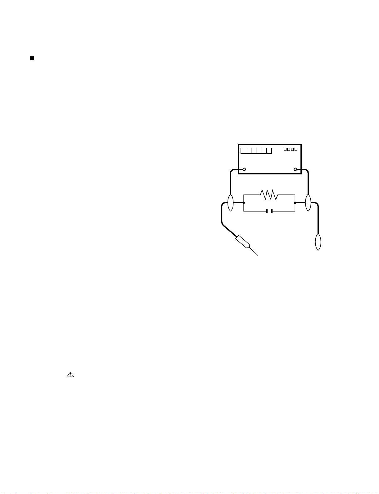
5. To be sure that no shock hazard exists, check for leakage current in
the following manner.
• Plug the AC cord directly into a 110 ~ 240 volt AC outlet.
• Using two clip leads, connect a 1.5k ohm, 10 watt resistor paralleled by a 0.15µF capacitor in series with all exposed metal cabinet
parts and a known earth ground, such as electrical conduit or electrical ground connected to an earth ground.
• Use an AC voltmeter having with 5000 ohm per volt, or higher, sensitivity or measure the AC voltage drop across the resistor.
• Connect the resistor connection to all exposed metal parts having a
return to the chassis (antenna, metal cabinet, screw heads, knobs
and control shafts, escutcheon, etc.) and measure the AC voltage
drop across the resistor.
All checks must be repeated with the AC cord plug connection
reversed. (If necessary, a non polarized adaptor plug must be used
only for the purpose of completing these checks.)
Any reading of 0.74 Vrms (this corresponds to 0.5 mA rms AC.) or
more is excessive and indicates a potential shock hazard which
must be corrected before returning the monitor to the owner.
DVM
AC SCALE
1.5k ohm
10W
0.15µF
TEST PROBE
TO EXPOSED
METAL PARTS
CONNECT TO
KNOWN EARTH
GROUND
///////////////////////////////////////////////////////////////////////////////////////////////////////////////////////////////////////////////////////////////////////////////////////////////////////////////////////////////////////////
SAFETY NOTICE
Many electrical and mechanical parts in LCD color television have
special safety-related characteristics.
These characteristics are often not evident from visual inspection, nor
can protection afforded by them be necessarily increased by using
replacement components rated for higher voltage, wattage, etc.
Replacement parts which have these special safety characteristics are
identified in this manual; electrical components having such features
are identified by " " and shaded areas in the Replacement Parts
Lists and Schematic Diagrams.
For continued protection, replacement parts must be identical to those
used in the original circuit.
The use of a substitute replacement parts which do not have the same
safety characteristics as the factory recommended replacement parts
shown in this service manual, may create shock, fire or other hazards.
///////////////////////////////////////////////////////////////////////////////////////////////////////////////////////////////////////////////////////////////////////////////////////////////////////////////////////////////////////////
i
Page 3
LC-26/32A37M
PRECAUTIONS FOR USING LEAD-FREE SOLDER
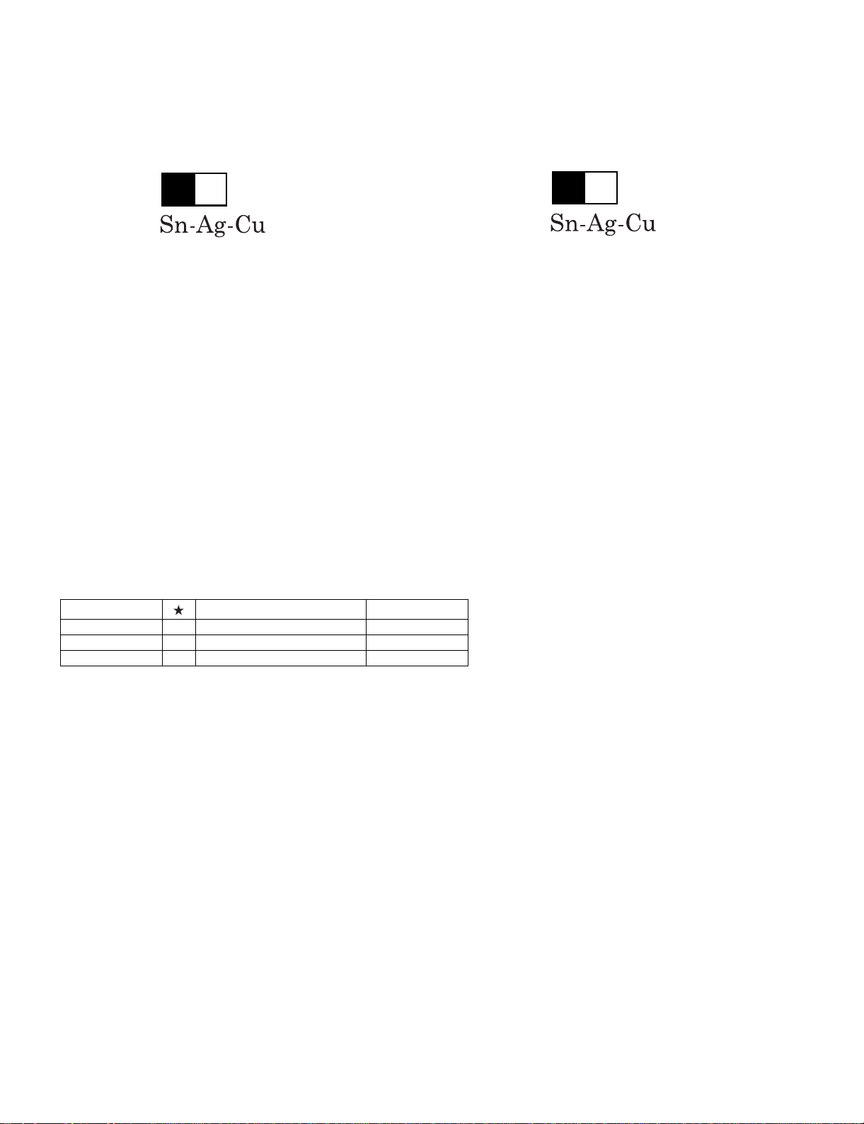
Employing lead-free solder
• “All PWBs” of this model employs lead-free solder. The LF symbol indicates lead-free solder, and is attached on the PWBs and service manuals.
The alphabetical character following LF shows the type of lead-free solder.
Example:
L Fa
Indicates lead-free solder of tin, silver and copper.
Indicates lead-free solder of tin, silver and copper.
L F a/a
Using lead-free wire solder
• When fixing the PWB soldered with the lead-free solder, apply lead-free wire solder. Repairing with conventional lead wire solder may cause damage or accident due to cracks.
As the melting point of lead-free solder (Sn-Ag-Cu) is higher than the lead wire solder by 40 °C, we recommend you to use a dedicated soldering
bit, if you are not familiar with how to obtain lead-free wire solder or soldering bit, contact our service station or service branch in your area.
Soldering
• As the melting point of lead-free solder (Sn-Ag-Cu) is about 220 °C which is higher than the conventional lead solder by 40 °C, and as it has poor
solder wettability, you may be apt to keep the soldering bit in contact with the PWB for extended period of time. However, Since the land may be
peeled off or the maximum heat-resistance temperature of parts may be exceeded, remove the bit from the PWB as soon as you confirm the
steady soldering condition.
Lead-free solder contains more tin, and the end of the soldering bit may be easily corroded. Make sure to turn on and off the power of the bit as
required.
If a different type of solder stays on the tip of the soldering bit, it is alloyed with lead-free solder. Clean the bit after every use of it.
When the tip of the soldering bit is blackened during use, file it with steel wool or fine sandpaper.
• Be careful when replacing parts with polarity indication on the PWB silk.
Lead-free wire solder for servicing
Part No. Description Code
ZHNDAi123250E J φ0.3mm 250g (1roll) BL
ZHNDAi126500E J φ0.6mm 500g (1roll) BK
ZHNDAi12801KE J φ1.0mm 1kg (1roll) BM
ii
Page 4
LC-26/32A37M
LC26A37M
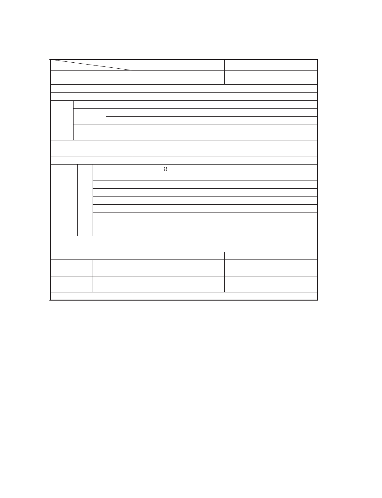
CHAPTER 1. SPECIFICATIONS
[1] SPECIFICATIONS
ServiceManual
Item
LCD panel
Resolution
Video Colour System PAL/SECAM/NTSC 3.58/NTSC 4.43/PAL 60
TV
Function
Viewing angles H : 176º V : 176º
Audio amplifier
Speakers
Terminals Rear Antenna input
OSD language English/Simplified Chinese/Traditional Chinese/Arabic
Power Requirement AC 110—240 V, 50/60 Hz
Power Consumption 88 W (0.9 W Standby) 97 W (0.9 W Standby)
Dimensions
Weight
Operating Temperature 0°C — 40°C
• As a part of policy of continuous improvement, SHARP reserves the right to make design and specification changes for
product improvement without prior notice. The performance specification figures indicated are nominal values of production
units. There may be some deviations from these values in individual units.
TV-Standard PAL: B/G, D/K, I SECAM: B/G, D/K, K/K
Receiving
Channel
TV-Tuning System Auto Preset 99 ch
STEREO/BILINGUAL NICAM: B/G, I, D/K A2 stereo: B/G
INPUT1
INPUT2
INPUT3
INPUT4
INPUT 5 S-VIDEO in, VIDEO in, AUDIO in
INPUT 6 (PC input)
OUTPUT AUDIO out
RS-232C 9 pin D-sub male connector
without stand
with stand
without stand 7.5 kg 9.5 kg
with stand 9.0 kg 11.0 kg
Model
VHF/UHF 42.75—866.25 MHz
CATV S1—S41ch (including Hyperband)
LC-26A37M LC-32A37M
26" (640 mm) Advanced Super
View & BLACK TFT LCD
1,049,088 pixels (1366 x 768)
10Wx2
10 x 4 cm 2pcs
UHF/VHF 75
HDMI (HDMI input) (480I, 576I, 480P, 576P, 720P/50Hz, 720P/60Hz, 1080I/50Hz, 1080I/60Hz)
HDMI (HDMI input) (480I, 576I, 480P, 576P, 720P/50Hz, 720P/60Hz, 1080I/50Hz, 1080I/60Hz)
AUDIO in, COMPONENT in (480I, 576I, 480P, 576P, 720P/50Hz, 720P/60Hz, 1080I/50Hz, 1080I/60Hz)
AUDIO in, COMPONENT in (480I, 576I, 480P, 576P, 720P/50Hz, 720P/60Hz, 1080I/50Hz, 1080I/60Hz)
15 pin mini D-sub, AUDIO in (common use with INPUT 1) (Ø 3.5 mm jack)
652 (W) x 445 (H) x 123 (D) mm 788 (W) x 519 (H) x 123 (D) mm
652 (W) x 504 (H) x 235 (D) mm 788 (W) x 575 (H) x 235 (D) mm
DIN type
32" (800 mm) Advanced Super
View & BLACK TFT LCD
1
NTSC: M
1 – 1
Page 5
LC26A37M
CHAPTER 2. OPERATION MANUAL
[1] OPERATION MANUAL
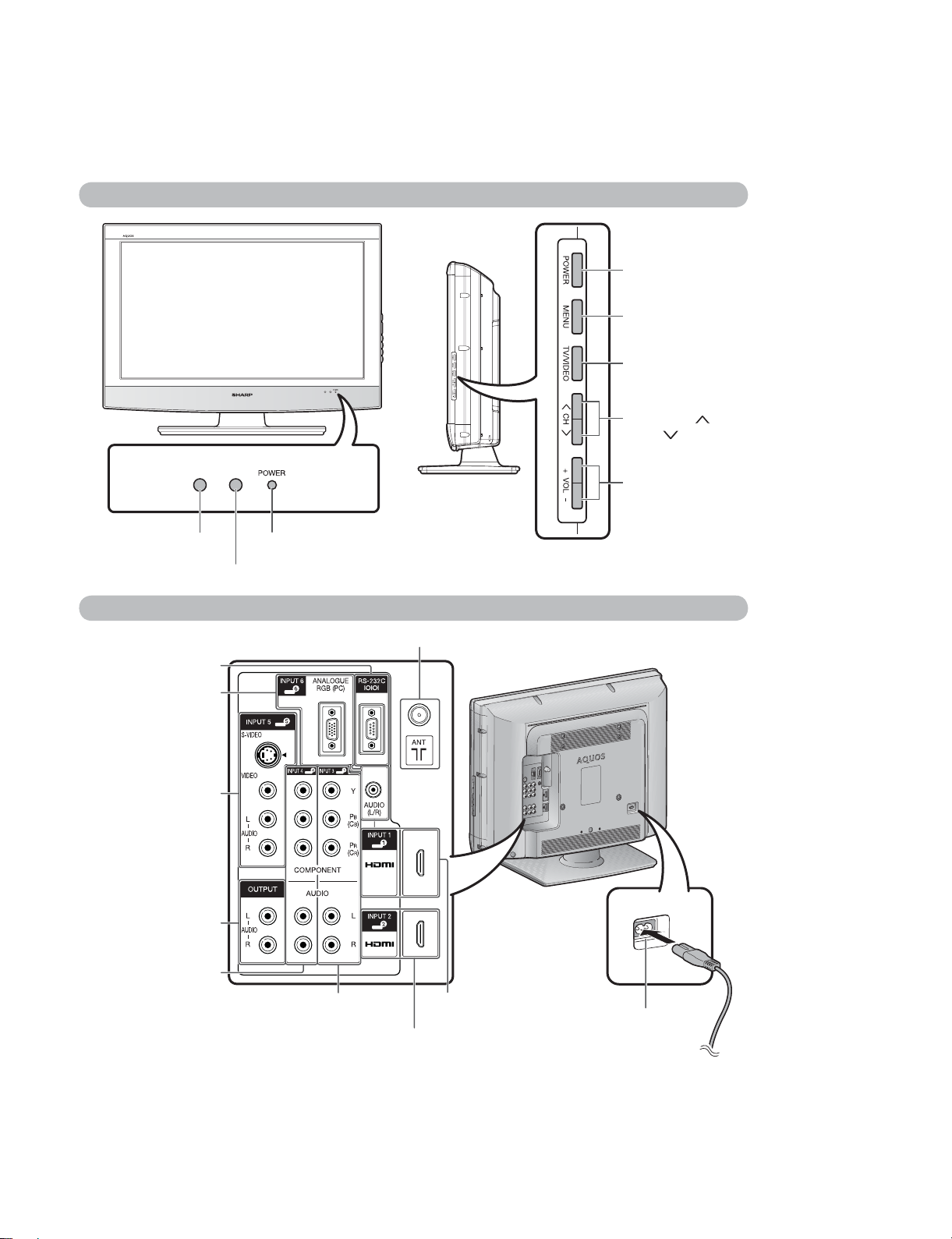
1. Part Names
TV (Front/Side)
LC-26/32A37M
ServiceManual
POWER (On/Off)
button
MENU button
TV/VIDEO button
Channel up( )/
down ( ) buttons
Volume up (+)/
down (-) buttons
Remote control sensor
OPC sensor
TV (Rear)
RS-232C terminal
INPUT 6 (PC) terminals
INPUT 5 terminals
OUTPUT terminals
INPUT 4 terminals
POWER indicator
Antenna input terminal
INPUT 3 terminals
INPUT 2 (HDMI) terminal
INPUT 1 (HDMI)
terminal
2 – 1
AC INPUT terminal
Page 6
LC-26/32A37M
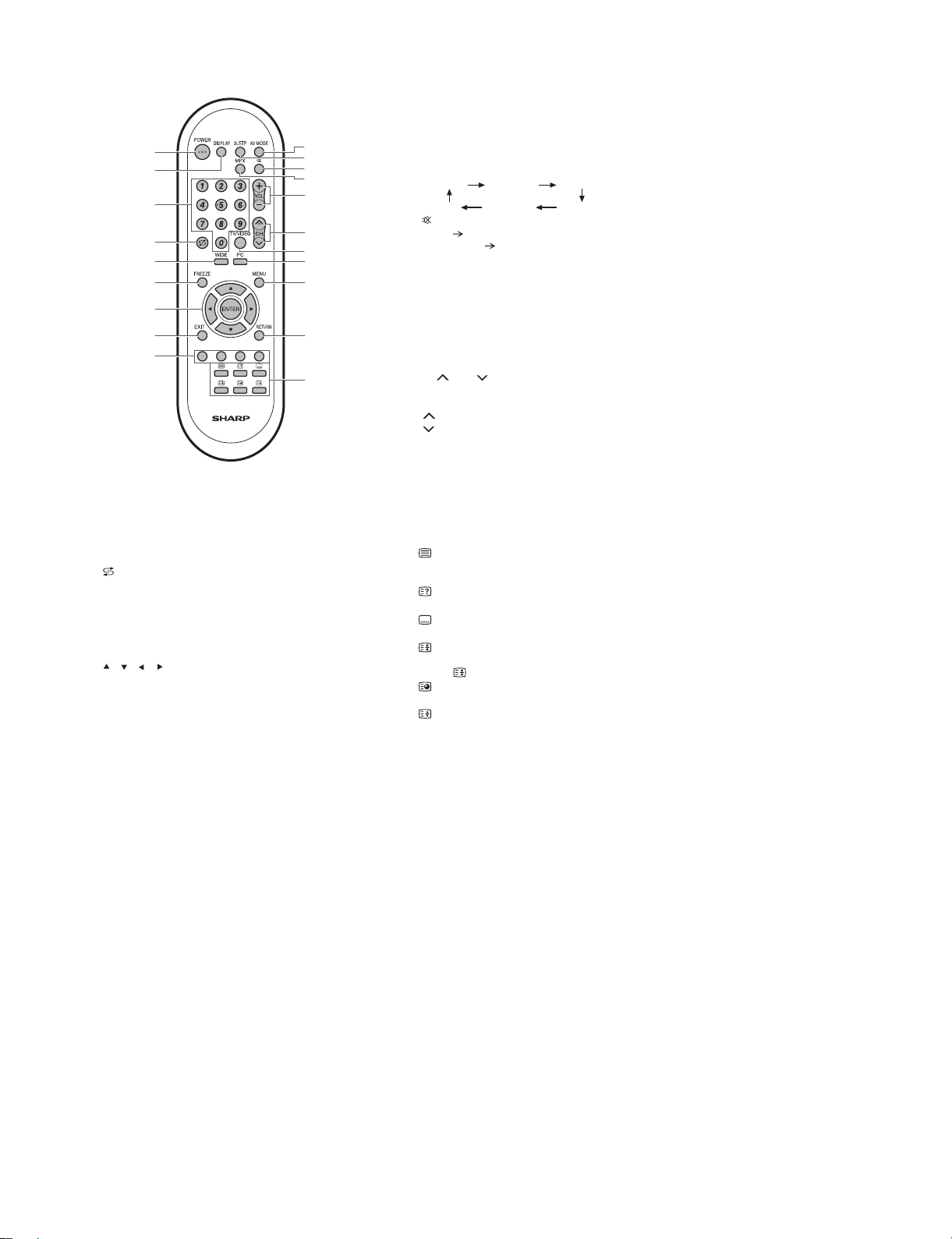
2. Remote Control Unit
1
2
3
4
5
6
7
8
9
1 POWER (STANDBY/ON)
To switch the power on and off.
2 DISPLAY
Display the channel or input information.
30–9
Set the channel.
TELETEXT mode: Set the page.
4 (Flashback)
Press to return to the previous selected channel or
external input mode.
5WIDE
Change the wide image mode.
6 FREEZE
Freeze a motion picture on the screen.
7///(Cursor)
Select a desired item on the setting screen.
ENTER
Execute a command.
8 EXIT
Return to the default screen.
10
11
12
13
14
15
16
17
18
19
20
9 Colour (Red/Green/Yellow/Blue)
TELETEXT mode: Select a page.
10 AV MODE
Select an audio and video setting.
11 SLEEP
Set the Sleep timer.
0hr.30min. 1hr.00min.
Off
12 (Mute)
Press Mutes sound.
Press again Restores sound.
Mute will be cancelled after 30 minutes. However, the TV will
not suddenly output loud sound as the volume level will be set
to 0 automatically. Increase the volume level by pressing VOL +.
13 MPX
Select the sound multiplex mode.
14 VOL + /VOL -
Set the volume.
(+)Increasethevolume.
( - ) Decrease the volume.
15 CH /C H
TV input mode: Select the channel.
TELETEXT mode: Select the page.
( ) Increase the channel number.
( ) Decrease the channel number.
16 TV/VIDEO (INPUT SOURCE)
Select an input source.
17 PC
Directly select the PC terminal.
18 MENU
Display the menu screen.
19 RETURN
MENU mode: Return to the previous menu screen.
20 (TELETEXT)
Select the TELETEXT mode. (all TV image, all TEXT image,
TV/TEXT image)
(Reveal hidden for TELETEXT)
TELETEXT mode: Display hidden characters.
(SUBTITLE for TELETEXT)
To turn the subtitles on and off.
(Hold)
TELETEXT mode: Stop updating Teletext pages automatically.
Press again to release the hold mode.
(Subpage)
Display the Teletext subpage directly.
(Top/Bottom/Full)
TELETEXT mode: Set the area of magnification.
2hr.30min.
1hr.30min.
2hr.00min.
2 – 2
Page 7
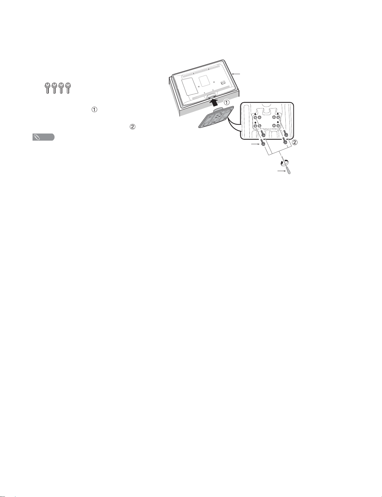
3. Attaching The Stand
• Before attaching (or detaching) the stand, unplug the AC cord from the AC INPUT terminal.
• Before performing work spread cushioning over the base area to lay the TV on. This will prevent it from
being damaged.
Confirm the screws supplied with the TV.
1
Screws (x4)
(used in step 3)
Insert the stand base to the stand post on the
2
bottom of the TV. ( )
Insert and tighten the 4 screws into the 4 holes
3
on the bottom of the stand base.( )
NOTE
• To detach the stand, perform the steps in reverse order.
Soft
cushion
Screw
Screw driver
LC-26/32A37M
2 – 3
Page 8
LC-26/32A37M
LC26A37M
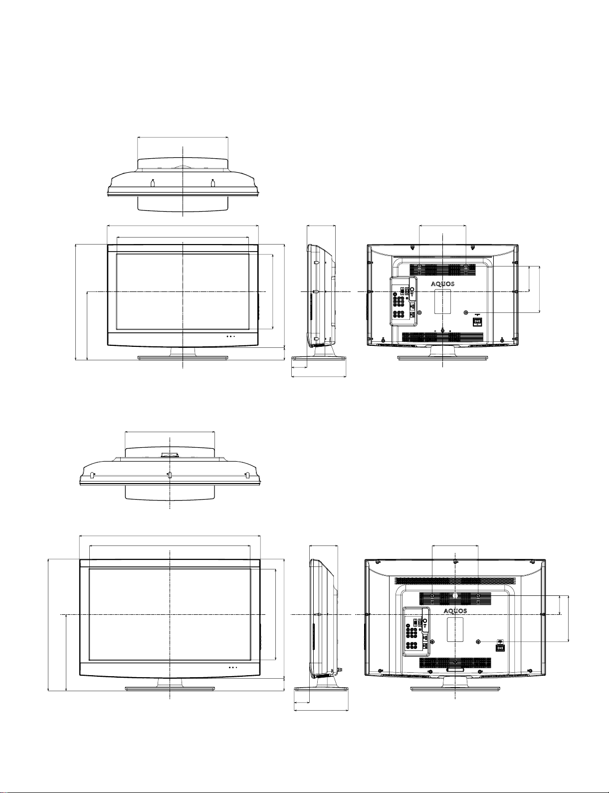
CHAPTER 3. DIMENSIONS
[1] DIMENSIONS
ServiceManual
LC-26A37M
504
299
390
652 123 200
567.9
320.6
445
59
66
235
Unit: mm
110
200
LC-32A37M
575
334
390
788
699.2
393.8
51959
123 200
82
200
66
3 – 1
235
Page 9
LC26A37M
CHAPTER 4. REMOVING OF MAJOR PARTS
ServiceManual
[1] REMOVING OF MAJOR PARTS
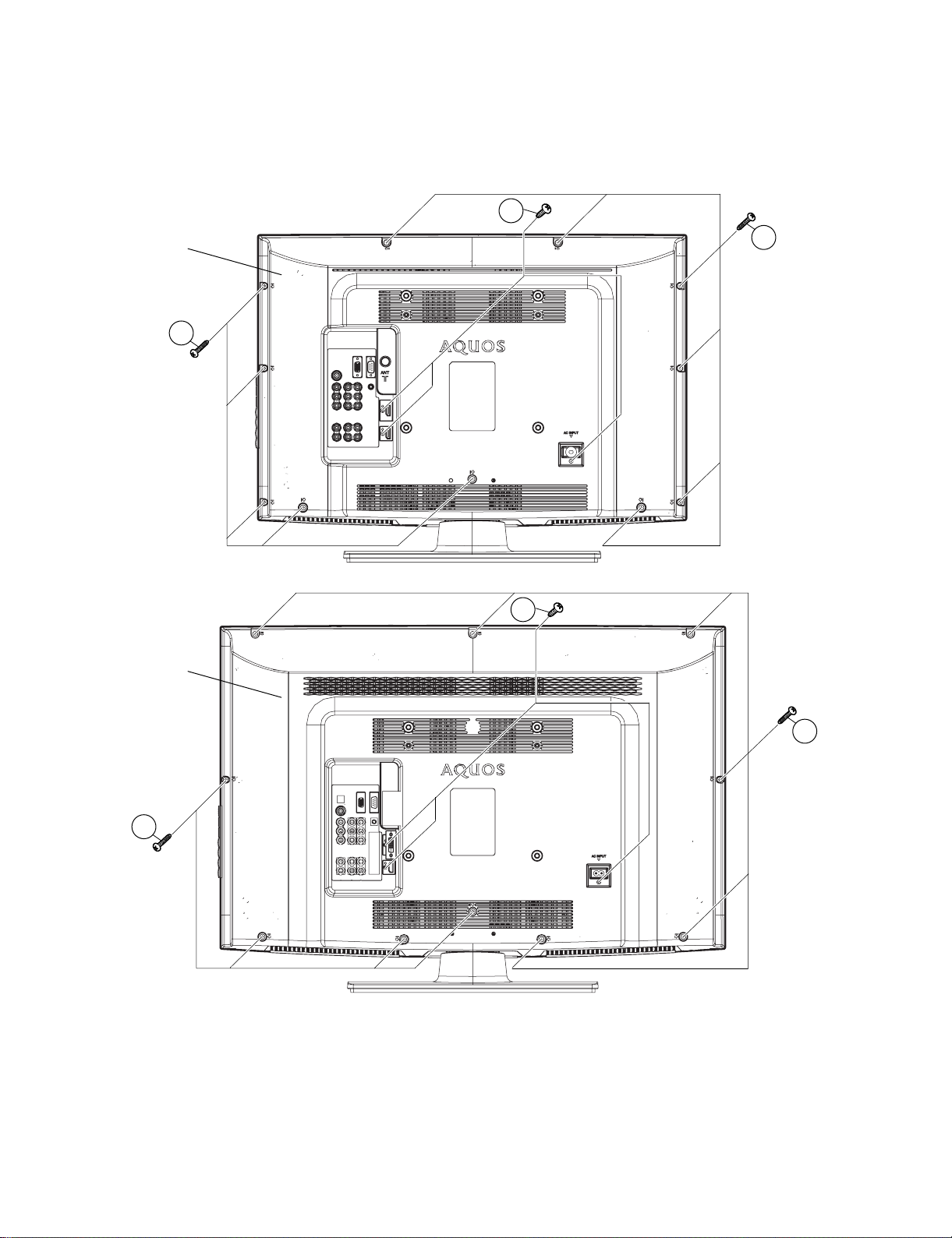
1. REMOVING OF REAR CABINET
1. Remove the 11 (LC-26A37M)/10 (LC-32A37M) screws [1], 3 screws [2] and detach the Rear Cabinet.
LC-26/32A37M
LC-26A37M
Rear Cabinet
LC-32A37M
2
1
1
2
Rear Cabinet
1
1
4 – 1
Page 10

LC-26/32A37M
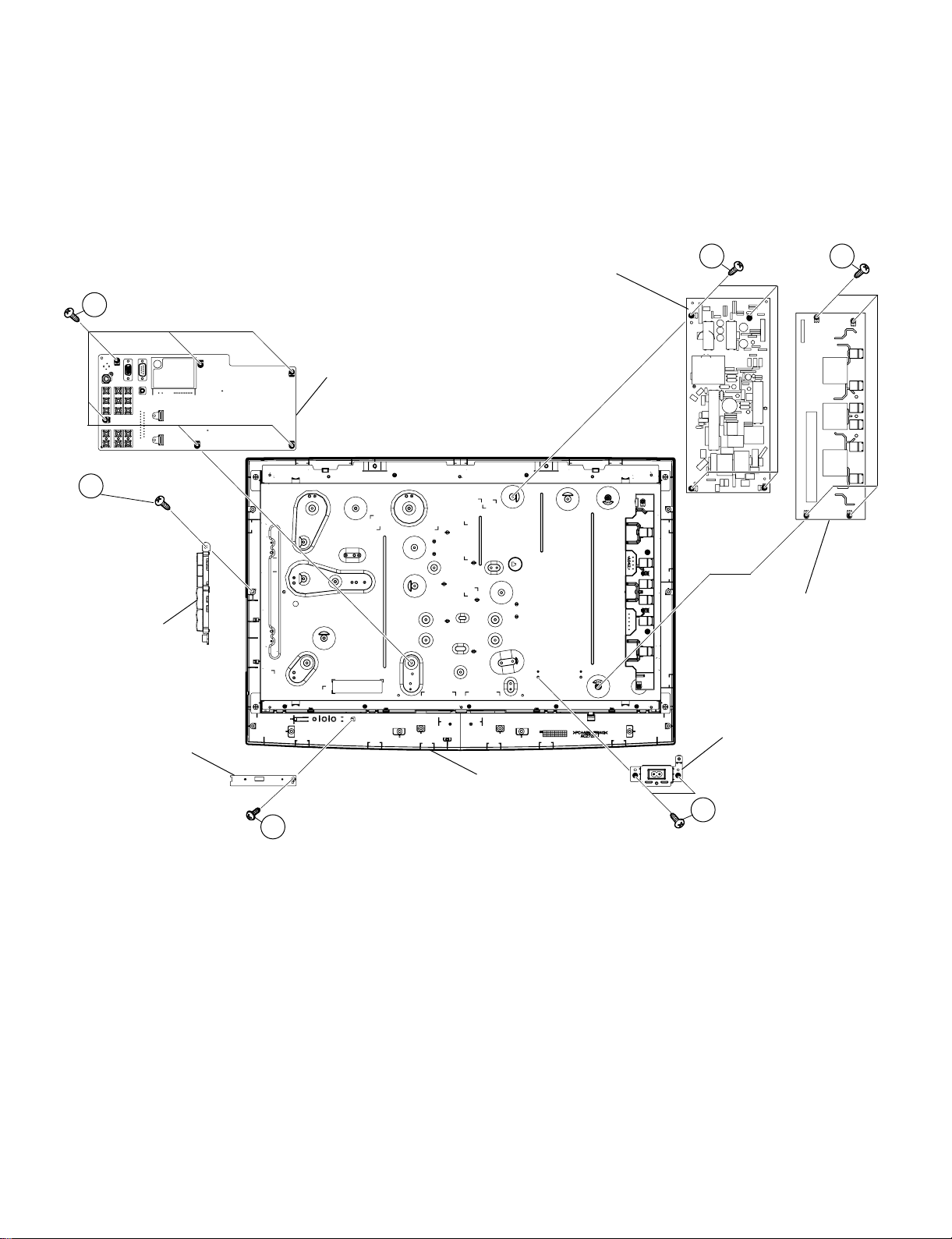
2. REMOVING OF CONNECTORS, SPEAKERS, STAND COVER ASS’Y AND STAND ASS’Y
1. Remove all the connectors from all the PWBs.
2. Remove 2 screws [1] and detach the Speaker-L and Speaker-R.
3. Remove the 4 screws [2], 4 screws [3] and detach the Stand Cover Ass’y.
4. Remove the 4 screws [4] and detach the Stand Ass’y.
POWER PWB Unit
MAIN PWB Unit
KEY PWB Unit
R/C, LED PWB Unit
Speaker-R
3
䬌䎳䎚䎕䎓䎕䬍
䬌䎳䎚䎕䎓䎔䬍 䬌䎦䎱䎚䎖䎓䎕䬍
䬌䎳䎧䬍
䬌䎶䎳䬍
䬌䎳䎚䎓䎓䎔䬍
INVERTER PWB Unit
Speaker-L
䬌䎮䎰䬍
䬌䎵䎤䬍
䬌䎶䎳䬍
䬌䎳䎕䎖䎓䎔䬍
䬌䎳䎛䎕䎓䎔䬍
䬌䎦䎱䎔䬍 䬌䎦䎱䎕䬍
䬌䎳䎛䎕䎓䎕䬍
䬌䎶䎳䬍
1
1
Stand Cover Ass'y
2
3
Stand Ass'y
4
*The shown is LC-26A37M
4 – 2
Page 11
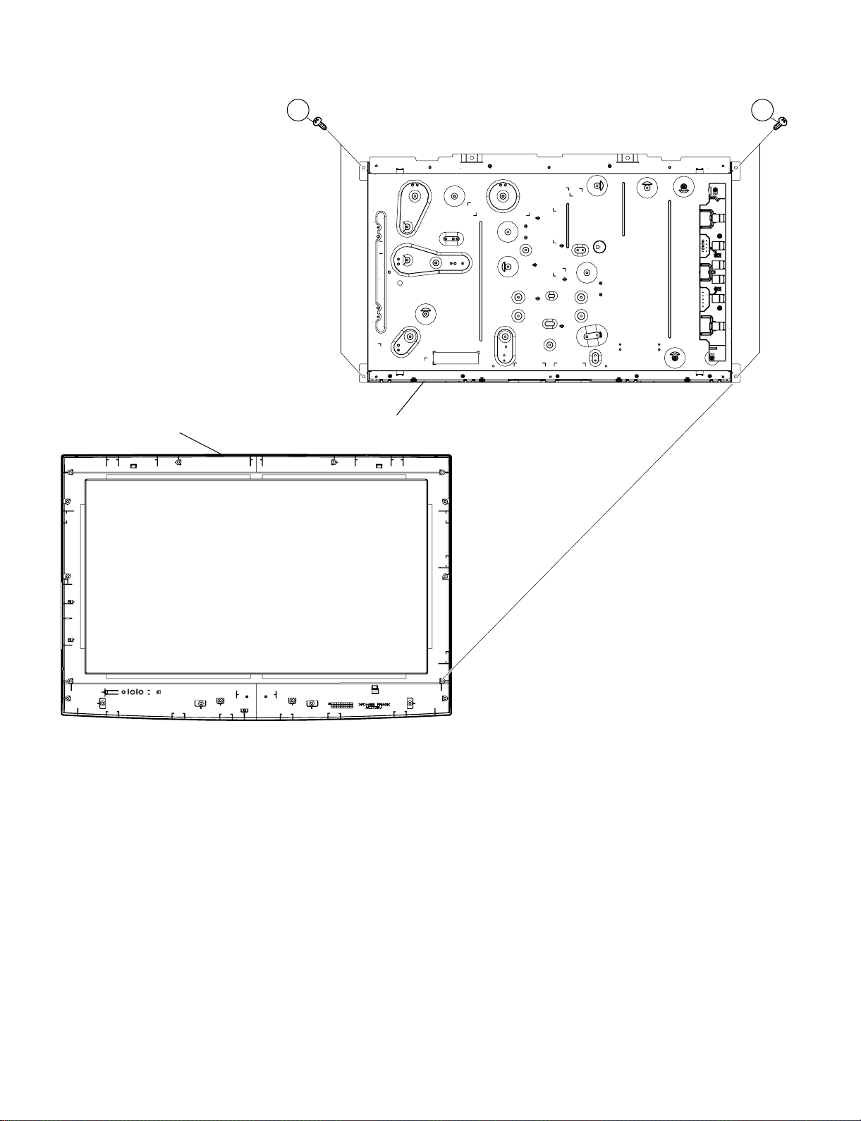
3. REMOVING OF PWB UNITS
1. Remove the 1 screw [1] and detach the R/C, LED PWB Unit.
2. Remove the 6 screws [2] and detach the MAIN PWB Unit.
3. Remove the 4 screws [3] and detach the POWER PWB Unit.
4. Remove the 4 screws [4] and detach the INVERTER PWB Unit.
5. Detach the KEY PWB Unit (LC-26A37M).
Remove the 1 screw [5] and detach the KEY PWB Unit (LC-32A37M).
6. Remove the 2 screws [6] and detach the SW Bracket.
LC-26/32A37M
2
(LC-32A37M only)
5
KEY PWB Unit
MAIN PWB Unit
POWER PWB Unit
3 4
INVERTER PWB Unit
R/C, LED PWB Unit
SW Bracket
Front Cabinet
6
1
*The shown is LC-26A37M
4 – 3
Page 12
LC-26/32A37M
4. REMOVING OF LCD PANEL UNIT
1. Remove the 4 screws [1] and detach the LCD Panel Unit from Front Cabinet.
Front Cabinet LCD Panel Unit
11
4 – 4
*The shown is LC-26A37M
Page 13

LC-26/32A37M
LC26A37M
CHAPTER 5. ADJUSTMENT PROCEDURE
ServiceManual
[1] ADJUSTMENT PROCEDURE
1. Adjustment method after PWB and/or IC replacement due to repair
The unit is set to the optimum at the time of shipment from the factory. If any value should become improper or any adjustment is necessary due to
the part replacement, make an adjustment according to the following procedure.
1. Procure the following units in order to replace the main unit, IC3001and IC1951.
MAIN UNIT: DUNTKF067FM04 (LC-26A37M)
DUNTKF067FM05 (LC-32A37M)
NOTE: [Caution when replacing ICs in the main unit (IC2304/IC1902/IC1922)]
The above ICs are EEPROMs storing the EDID data of HDMI and the monitor microcomputer. Before replacing the relevant part, procure the
following parts in which the data have been rewritten.
IC2304 RH-IXC818WJQZS PC EDID
IC1902 RH-IXC819WJQZS HDMI EDID
IC1922 RH-IXC820WJQZS HDMI EDID
2. After replacing the LCD panel or LCD control PWB, check PANEL_SIZE in the following procedure.
1) Enter the process adjustment mode.
2) Use the cursor keys / and CH / of R/C to select the item [Inch Setting] on the page 2/11.
3) Verify that the panel size is displayed.
4) If the size doesn't match, select the values of the panel size with the Vol +/- keys.
5) After selection in Step 4), press the ENTER key, and it is completed with OK displayed.
3. After replacing the LCD panel, adjust the VCOM in the following procedure.
1) Enter the process adjustment mode.
2) Use the cursor keys / and CH / of R/C to select the item [ VCOM ADJ] on the page 11/11.
3) Press the ENTER key to verify that the adjustment pattern is displayed.
4) Use the +/- keys of VOL of R/C to adjust the flicker in the center of the screen to minimum.
5) When the optimal state is achieved in Step 4, press the ENTER key to turn the pattern to OFF.
5 – 1
Page 14
LC-26/32A37M
2. Entering the adjustment process mode
There are 2 ways as follows:
• After power-on, press “ADJUSTMENT PROCESS” key of the remote control.
• During servicing.
1
While holding down the TV/VIDEO and DOWN keys at the same time, set the Power switch to ON. (“K” standing for inspection process mode is
displayed in the upper left position of the screen.) → Press the Channel DOWN and Volume DOWN keys at the same time. (The adjustment process mode screen appears.)
To cancel it, turn off the power using the Power switch or remote control.
3. Remote controller key operation and description of display in adjustment process mode.
1. key operation
Remote controller key Main unit key Function
CH ( / )
VOL (+ / –) VOL (+ / –) Changing a selected line setting (+1/-1)
Cursor ( / )
Cursor ( / )
TV/INPUT button on remote
controller
OK —————— Executing a function
* Input mode is switched automatically when relevant adjustment is started so far as the necessary input signal is available.
CH ( / ) Moving an item (line) by one (UP/DOWN)
—————— Turning a page (PREVIOUS/NEXT)
—————— Changing a selected line setting (+10/-10)
TV/INPUT button Input source switching (toggle switching)
2
(TV→INPUT1→INPUT2→INPUT3→INPUT4→INPUT5→INPUT6)
2. Description of display
(1) Current page/Total pages (3) Currently selected input
(4) Current colour TV system
(2) Current page title
1/11
Main Version
Checsum Value
TCON Version
TEMP SENSOR
NORMAL STANDBY CAUSE
ERROR STANDBY CAUSE
[INFO] TV AUTO XX:ASIA
LEW07 01.XX (XX/XX/XXX)
XX
XX
XX
XX
XX
[1] 0
[2] 0
[3] 0
[4] 0
[5] 0
00H 00M
00H 00M
00H 00M
00H 00M
00H 00M
(5) Inch/Destination
Adjustment process
menu header
(7) Parameters
5 – 2
Page 15
LC-26/32A37M
4. Adjustment process mode menu
The character string in brackets [ ] will appear as a page title in the adjustment process menu header.
Page Line Item Description Remarks (adjustment detail, etc.)
1/11 [INFO]
1 Main Version JraAS XXX(XX/XX/XX) Main microprocessor version
2 Checksum Value XX DTV microprocessor version
3 TCON Version XX DTV micr oprocessor-Loader version
4 TEMP SENSOR xxxxxx
5 NORMAL STANDBY CAUSE RC_STANDBY
6 ERROR STANDBY CAUSE [1] 00H 00M Error standby cause Total operating time before error
[2] 00H 00M
[3] 00H 00M
[4] 00H 00M
[5] 00H 00M
2/11 [INIT]
1 Factory Init [HONG KONG/CHINA/ASIA] Initialization to factory settings execution
2 Inch Setting XX Inch present setting
3 Public Mode OFF/ON HOTEL MODE flag setting
4 Center Acutime xxH xxM Main operating hours
5 RESET OFF/ON Main operating hours reset
6 Backlight Acutime xxH xxM Backlight operating hours
7 RESET OFF/ON Backlight operating hours reset
8 Picture Read Pos X 0-xxx x-axis setting of picture data
9 Picture Read Pos Y 0-xxx y-axis setting of picture data
10 Picture Read ON/OFF Start/stop of picture data
3/11 [PAL.SECAM.N358]
1 RF-AGC ADJ ENTER RF-AGC auto adjustment execution
2 PAL+TUNER ADJ ENTER PAL TUNER auto adjustment execution
3 PAL ADJ ENTER PAL auto adjustment execution
4 TUNER ADJ ENTER TUNER auto adjustment execution
5 CONTRAST SD 32 PAL contrast adjustment
6 SECAM CB OFFSET 1 SECAM offset adjustment
7 SECAM CR OFFSET 1 SECAM offset adjustment
8 TUNER A DAC 32 TUNER DAC adjustment
9 RF AGC 16 RF AGC adjustment
4/11 [COMP 15K]
1 COMP 15K ADJ ENTER COMP15K auto adjustment execution (No use)
2 COMP 15K CONTRAST 40 Contrast adjustment
5/11 [HDTV]
1 HDTV CONTRAST 41 HDTV Contrast adjustment
6/11 [SMPTE]
1 RF-AGC ADJ ENTER RF-AGC auto adjustment execution
2 PAL-AGC ADJ ENTER PAL AGC auto adjustment execution (No use)
3 PAL ADJ ENTER PAL auto adjustment execution
4 TUNER ADJ ENTER TUNER auto adjustment execution
5 CONTRAST SD 30 PAL contrast adjustment
6 SECAM CB OFFSET 1 SECAM offset adjustment
7 SECAM CR OFFSET 1 SECAM offset adjustment
8 TUNER A DAC 36 TUNER DAC adjustment
9 RF AGC 16 RF AGC adjustment
7/11 [M GAMMA INFO]
1 M GAMMA IN 6 928 W/B adjustment, gradation 6 input setting
2 M GAMMA WRITE OFF/ON EEP writing of adjustment values
3 M GAMMA RESET OFF/ON Initialization of adjustment values
8/11 [M GAMMA 1-3]
1 M GAMMA R 2 0 W/B adjustment, gradation 2R adjustment value
2 M GAMMA G 2 0 W/B adjustment, gradation 2G adjustment value
3 M GAMMA B 2 0 W/B adjustment, gradation 2B adjustment value
4 M GAMMA WRITE OFF/ON EEP writing of adjustment values
9/11 [M GAMMA 4-6]
1 M GAMMA R 6 0 W/B adjustment, gradation 6R adjustment value
2 M GAMMA G 6 0 W/B adjustment, gradation 6G adjustment value
3 M GAMMA B 6 0 W/B adjustment, gradation 6B adjustment value
4 M GAMMA WRITE OFF/ON EEP writing of adjustment values
5 – 3
Page 16
LC-26/32A37M
Page Line Item Description Remarks (adjustment detail, etc.)
10/11 [ETC]
1 EEP CLEAR OFF/ON Clear of all adjustment value
2 EEP CLEAR B OFF/ON Clear of adjustment value of B mode
3 STANDBYCAUSE RESET OFF/ON Reset of STANDBY CAUSE
4 AUTO INSTALLATION SW 0/1 1: * * * 0: * * *
5OPTION 0
6 COUNTRY HONG KONG/CHINA/ASIA Destination setting
7 L ERR RESET 0 LAMP ERR RESET Initializatio of L_ERR
8 L ERR STOP 0/1 LAMP ERR Inhibit L_LRR detection
9 I2C-OFF ENTER I2C DATA execution
11/11 [COM-BIAS]
1VCOM ADJ 63
2 TEST PATTERN 0
5. Special features
* ERROR STANDBY CAUSE (Page 1/11)
The total time when the unit enters the standby due to operational error and cause of error are recorded on EEPROM as much as possible.
The values can be used to locate the fault for repair.
* EEP CLEAR (Page10/11)
Clear of process adjustment EEP value.
6. Lamp error detection
1. Function
This LCD colour TV set incorporates a lamp error detection feature that automatically turns off the power for safety under abnormal lamp or lamp
circuit conditions. If by any chance anything is wrong with the lamp or lamp circuit or if the lamp error detection feature is activated for some reason, the following will result.
1) The powe r is interrupted in about 6 seconds after it is turned on.
(The power LED on the front of the TV set turns red from green and keeps blinking in red: ON for 250 ms and OFF for 1 sec.).
2) If the above phenomenon 1) occurs 5 times consecutively, it becomes impossible to turn on the power. (The power LED remained red).
2. Measures
1) Checking with lamp error detection OFF
Enter the adjustment process mode, referring to 1. Entering and exiting the adjustment process mode.
If there is a problem with the lamp or lamp circuit, the lamp will go out. (The power LED is green.)
Then, you can check the operation to see if the lamp and lamp circuit are in trouble.
2) Resetting the lamp error count
After the lamp and lamp circuit are found out of trouble, reset the lamp error count. If a lamp error is detected five consecutive times, the power
cannot be turned on. Using the cursor (UP/DOWN) key, move to the cursor to [LAMP ERROR RESET], Line 8 on adjustment process mode
service page 10/11. With the cursor (LEFT/RIGHT) keys, select the [LAMP ERROR RESET] value. Finally press the cursor (ENTER) ey s to
reset the value to “0”.
Table of contents of adjustment process mode Page 10/11.
[ETC]
EEP CLEAR OFF
EEP CLEAR B OFF
STANDBYCAUSE RESET OFF
AUTO INSTALLATION SW
OPTION
COUNTRY
L ERR RESET
0
0
HONG KONG
0
Resetting to "0"
L ERR STOP 0
I2C-OFF ENTER
5 – 4
Page 17
LC-26/32A37M
7. Standby Cause Function
This model is equipped with a STANDBY CAUSE FUNCTIONS which stores the cause of why the unit is turned off and displays it on adjustment process mode.
1. NORMAL STANDBY CAUSE
ERROR CODE here indicates cause of standby in normal operation or Function of the Unit.
No display when the unit is turned off with R/C.
Only the latest cause is indicated.
2. ERROR STANDBY CAUSE
ERROR CODE here indicates cause of Error in the unit.
It also indicates accumulated operating times of the unit.
The last five histories are displayed.
1)-5) five histories 1) is the latest.
When there is no error, error code is ‘0’ and no characters appear.
• NORMAL STANDBY CAUSE
Display Code Indication Description
1 RC_STANDBY in the cause of “Remote Controler OFF”
6 NO OPERATION in the cause of “NO OPERATION OFF”
7 NO SIGNAL in the cause of “NO SIGNAL OFF”
8 PC_MODE1 in the cause of “PC(INPUT6) POWER MANAGEMENT MODE1”
9 PC_MODE2 in the cause of “PC(INPUT6) POWER MANAGEMENT MODE2”
a SLEEP_TIMER in the cause of “SLEEP TIMER”
b RS232C in the cause of “RS232C COMMAND (POWR)”
• ERROR STANDBY CAUSE
Display Code Indication Description
1a TEMP_ERROR TEMPERATURE ERROR
1b LAMP_ERROR LAMP ERROR
5 – 5
Page 18
LC-26/32A37M
8. Video signal adjustment procedure
* The adjustment process mode menu is listed in Section 5.
1. Signal check
1) Signal generator level adjustment check (Adjustment to the specified level)
• Composite signal PAL : 0.7Vp-p ± 0.02Vp-p (Pedestal to white level)
• RGB signal : 0.7Vp-p ± 0.02Vp-p
• 15K component signal (50 Hz) : Y level : 0.7Vp-p ± 0.02Vp-p (Pedestal to white level)
: PB, PR level : 0.7Vp-p ± 0.02Vp-p
2. Entering the adjustment process mode
1) Enter the adjustment process mode according to Section 3.
3. RF AGC adjustment
Adjustment point Adjustment Conditions Adjustment procedure
1 Setting [Signal]
PAL
Sprit Field Colour Bar
RF signal UV
[Terminal]
TUNER
• Feed the PAL Sprit Field colour bar signal to TUNER.
Signal level: 55 dB µV +1dB, -1dB (75Ω LOAD)
[E-12CH]
2 Auto adjustment
performance
Adjustment process
Page3
㸡100% white
Bring the cursor on [ RF AGC ADJ] and press [OK]
[***OK***] appears when finished.
5 – 6
Page 19

LC-26/32A37M
9. White Balance Adjustment
Adjustment gradation values (IN) appear on page 7/11 of process adjustment, and adjustment initial values (offset value) appear on pages 8/11 and
9/11. For white balance adjustment, adjust the offset values on pages 8/11 and 9/11.
[Condition of the unit for inspection] Modulated light: MAX (+8)
[Adjustment reference device] Minolta CA-210
[Adjustment]
Check that the values on page 7/11 of process adjustment are set as below. If not, change them accordingly.
M GAMMA IN 2 320 M GAMMA IN 6 928
1) Display the current adjustment status at point 6. (Page 7/11 of process adjustment)
The display for checking the adjustment status is toggled by pressing the “6” button on the remote control.
(Normal OSD display → “6” → display for check (OSD disappears) → “6” →normal OSD display → • • •)
2) Read the value of the luminance meter.
3) Change M GAMMA R6/M GAMMA B6 (Adjustment offset value) on page 9/11 of process adjustment so that the values of the luminance meter
approach x = 0.272 and y = 0.277.
(Basically, G is not changed. If adjustment fails with R and B, change G. When G is lowered, the weaker of R and B must be fixed.)
4) If G is changed in step 3), change the values of M GAMMA G2 on pages 8/11 and 9/11 of process adjustment as follows. When not changed, go
to step5).
Offset value of M GAMMA G2 = (Offset value of M GAMMA G6) * (320/928)
5) Display the adju stment status of the current point 2. (Each time the “2” button on the remo te control is pressed, the adjustment status check display is toggled.)
(Normal OSD display → “2” → Check display (OSD disappears) → “2” → Normal OSD display → • • •)
Change M GAMMA R5/M GAMMA B2 (adjustment offset value) on page 9/11 of process adjustment so that the values of the luminance meter
approach x = 0.272 and y = 0.277.
[Adjustment reference standard value]
Adjustment spec ±0.004 Inspection spec ±0.006 (point 1)
Adjustment spec ±0.002 Inspection spec ±0.004 (Excluding the above-mentioned)
5 – 7
Page 20
LC-26/32A37M
10. Adjusting procedure by us e of [RS- 23 2C ]
1) Get ready the PC with COM port (RS-232C) running on Windows 95/98/ME/2000/XP operating system, as well as the RS-232C cross cable.
2) Start the unit with the RS-232C cable connected.
3) Start the terminal software. (The freeware readily available on the Internet will do.)
4) Make the following settings.
Baud rate 9,600 bps
Data LENGTH 8 bit
Parity bit None
Stop bit 1 bit
Flow control None
5) If the settings are correct, the terminal software indicates "ERR" against pressing of the "ENTER" key.
6) After the settings are done correctly, it is possible to make an adjustment by typing in the command shown in the table below and pressing the
"ENTER" key on the keyboard.
7) Command entry is successful if the terminal software indicates "OK" when the "ENTER" is pressed. If "ERR" is shown, retry to enter the command.
8) Send the process mode switching command to switch from the RS232C operation mode to the process mode.
KRSW0001: "ERR" is returned.
KKT10037: When "OK" is returned, the process mode becomes active. When "ERR", start over from KRSW0001.
9) Send each adjustment command.
RS-232C command list
Command Function Remarks
KYOF0000 Remote control disabled
OSDS0001 OSD display inhibited
SBSL0016 Light control level MAX
MSET0001 Background adjustment start
MSET0004 Initialization of adjustment value
LEV60928 Gradation 6 (928-gradation adjustment)
MG6G **** Adjustment of G of gradation 6 0000 ~4095
MG6R **** Adjustment of R of gradation 6 0000 ~ 4095
MG6B **** Adjustment of B of gradation 6 0000 ~ 4095
LEV20352 Gradation 2 (352-gradation adjustment)
MG2G **** Input of G of 2 Calculated value
MG2R **** Input of R of 2 0000 ~ 4095
MG2B **** Input of B of 2 0000 ~ 4095
MSET0003 Writing of adjustment value
5 – 8
Page 21
11. Initialization to factory settings
LC-26/32A37M
Caution: When the factory settings have been made, all user setting data, including the channel settings, are initialized.
After adjustments, exit the adjustment process mode.
To exit the adjustment process mode, unplug the AC power cord from the outlet to forcibly turn off the power.
When the power is turned off with the remote control, unplug the AC power cord and plug it back in (wait approximately 10 seconds before plugging
in the AC power cord)
(The adjustments done in the adjustment process mode are not initialized.) Keep this in mind when initializing these settings.
Adjustment item Adjustment conditions Adjustment procedure
1 Factory settings Forcibly turn off the power
(See to below caution)
• Enter the adjustment process mode.
• Move the cursor to [Factory Init] on page 2/11.
• Use the R/C key to select a destination [HONG KONG/CHINA/ASIA].
And, press the [OK] key.
• “EXECUTING...” appears and initialization starts.
• After a while, “*** OK ***” appears and the setting is complete.
NOTE: Never turn the power off during initialization.
When performing factory settings (while displaying page 2 of adjustment
process), confirm that the item “Inch Setting” or the panel size displayed
in the upper right corner corresponds to each panel size.
The following settings will be back to their factory ones.
1. User settings
2. Channel data (e.g. broadcast frequencies)
3. Maker option setting
4. Password data
5 – 9
Page 22
LC-26/32A37M
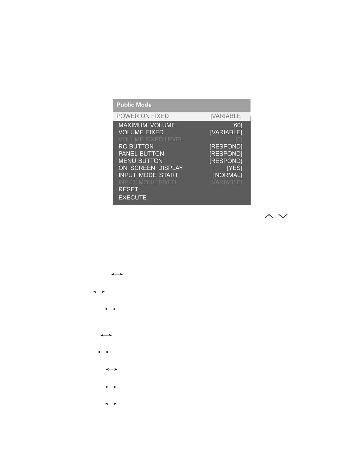
12. Public Mode (Hotel Mode)
1. How to Enter in the Public Mode (Hotel Mode).
Turn on the power and enter in the Adjustment Process mode as usual.
In the [INIT], Page 2/11 of Service, turns ON the Public Mode option.
Turn off TV by pressing Main Power switch.
While pressing “VOL+” and “INPUT” keys at the same time, press Main Power switch for more than 2 seconds.
Then, when you are asked for the password, enter “027”.
After this sequence the TV will turn on showing the Public Mode setting screen as follows:
Is possible to select each item of function by pressing cursor UP/DOWN keys on the remote control or CH( )( ) keys on the LCD TV.
(Except DTV)
The setting position of each item of functions is made by pressing cursor RIGHT/LEFT keys on the remote control or VOL (+) / (-) keys on the LCD
TV.
Select EXECUTE position after you set all function, and press cursor RIGHT/LEFT keys on the remote control or VOL (+) / (-) keys on the LCD TV
for confirmation.
2. Public Mode Settings.
1) POWER ON FIXED [VARIABLE FIXED]
When it is set to “FIXED” the TV is impossible to be switch off by Main Switch or Remote Control.
2) MAXIMUM VOLUME [0 60]
Is possible to set the maximum volume at limited level.
3) VOLUME FIXED [VARIABLE FIXED]
Is possible to fix the sound volume at limited level.
When “FIXED” is selected the sound volume before limited is fixed.
4) VOLUME FIXED LEVEL [0 60]
If “FIXED” has been selected, is possible to set a fixed volume at the level that is chosen.
5) RC BUTTON [RESPOND NO RESPOND]
If “NO RESPOND” is selected, the remote control keys are inoperative.
6) PANEL BUTTON [RESPOND NO RESPOND]
If “NO RESPOND” has been selected, the set’s keys remain deactivated (Except POWER key).
7) MENU BUTTON [RESPOND NO RESPOND]
If “NO RESPOND” has been selected, “MENU” key, of remote control, is inoperative.
8) ON SCREEN DISPLAY [YES NO]
If “NO” has been selected, the On Screen Display does not appear.
9) INPUT MODE START [NORMAL → TV (X) →DTV→ INPUT1 → INPUT2 → INPUT3 → INPUT4 → INPUT5]
When any other item than “NORMAL” has been selected, the sets will start in a selected input mode at the next power-on.
10)INPUT MODE FIXED [VARIABLE → FIXED]
“FIXED” has been selected, any channels and input modes other than those selected at the start mode cannot be picked up.
5 – 10
Page 23

LC-26/32A37M
11)RESET
Cancel all Public Mode settings. (It returns to the factory settings)
12)EXECUTE
Select this item, and press cursor RIGHT / LEFT keys on the remote control or VOL (+) / (-) keys on the LCD TV for confirmation the functions
settings.
5 – 11
Page 24
LC-26/32A37M
LC26A37M
CHAPTER 6. TROUBLESHOOTING TABLE
ServiceManual
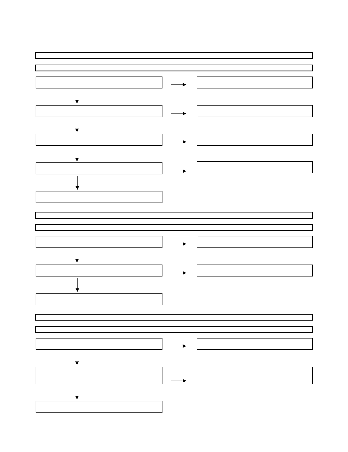
[1] TROUBLESHOOTING TABLE
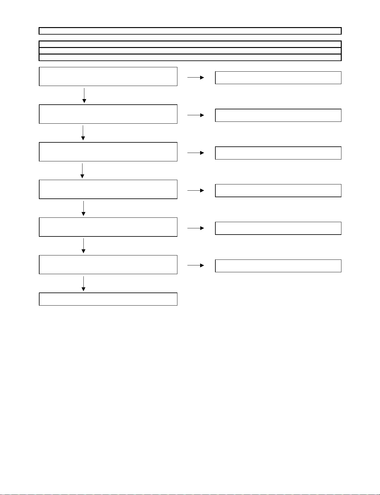
The sound is not emitted from the speaker though the picture has come out
No sound output in all modes?
Is the audio signal output of pins (28/L) and (27/R) of
IC3001 (MAIN_MICON) normal?
YES
Is the audio signal input to pin (3/L) and (7/R) of
IC2701 (AMP)?
YES
Is MUTE circuit [MUTE_SP_LINE,RESET_N_LINE]
normal? (Q2701, etc.)
YES
Is the audio signal output of pins (3,4)(L-Ch) and
(6,7)(R-ch) of P2701 (AOUDIO-CONNECTOR) normal ?
NO
NO
NO
NO
Check IC3001 and its peripheral circuits
Check the line between IC3001 and IC2701
Check the MUTE_SP_LINE and RESET_N_LINE
Check IC2701 and its peripheral circuits
YES
Check Speaker (right and left) and wire harness
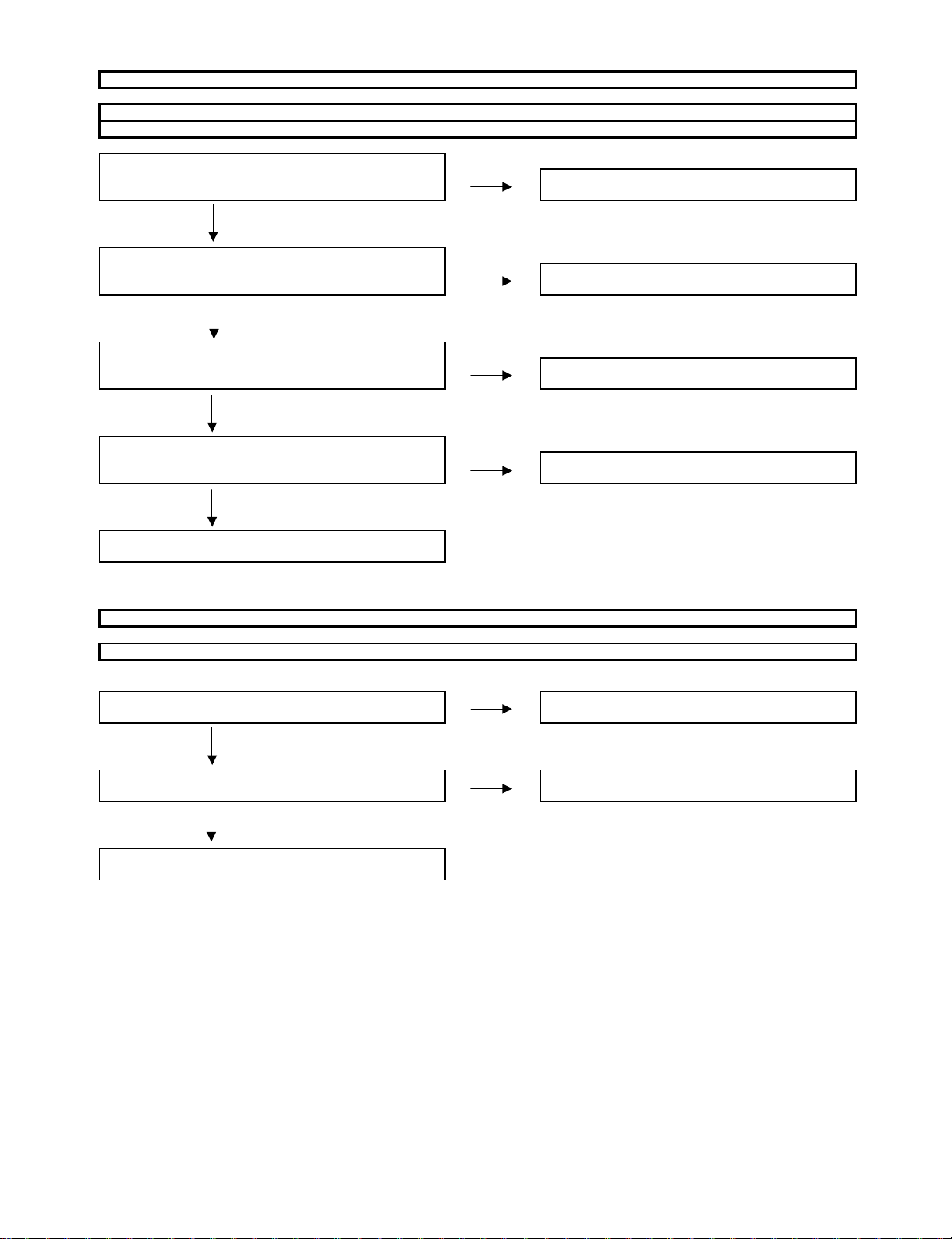
No sound (during the reception of TV (Analog) broadcasting)
Does not the sound go out through the picture has come out when UHF/VHF is receive?
Is the SIF signal output from pin (14) of TUNER
(TU201) replace as required
YES
Is the SIF signal sent to pins (31) of IC3001
(MAIN_MICON)?
YES
Refer to" No sound output in all modes".
No sound from external input devices (1)
Does not the sound of the audio signal input to INPUT1 / INPUT2 (HDMI) go out?
Is the picture of the signal input from INPUT1/
INPUT2 displayed? to (INPUT1/INPUT2) go out?
NO
NO
NO
Check the tuner and its peripheral circuits
Check line between TU201 and IC3001
Refer to " Does not the picture of the HDMI signal input
YES
Is the HDMI_SCK/WS/SD0 audio output from pin (86)
, (85),(84) of IC1915 (HDMI RECEIVER) to pin (39), MICON) and their peripheral circuits
(40), (38) of IC3001 (MAIN_MICON)?
YES
Refer to "No sound output in all modes".
NO
Check the line between IC1915 and IC3001 (MAIN
6 – 1
Page 25
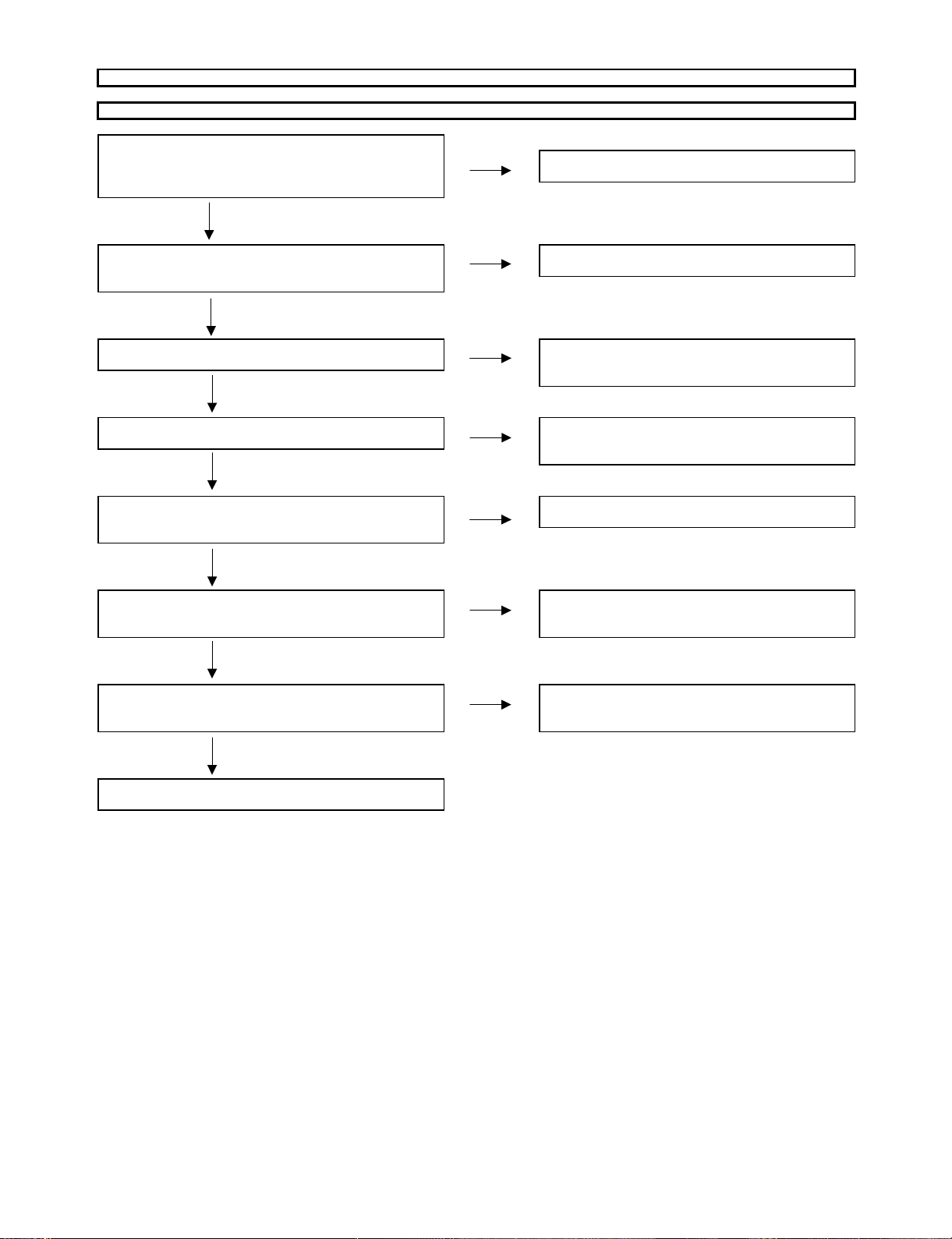
No sound from external input devices (2)
Does not the sound of the audio signal input to INPUT5 (J504) go out?
Does not the sound of the audio signal input to INPUT3 (J507) go out?
Does not the sound of the audio signal input to INPUT4 (J501) go out?
LC-26/32A37M
J504
Is the audio signal properly sent to pin (5) (AIN3L) and
(3) (AIN3_R) of (CVBS_IN) J504?
YES
J507
Is the audio signal properly sent to pin (5) (AIN1_L) and
(3) (AIN1_R) of (COMP1_AUDIO_IN) J507?
YES
J501
Is the audio signal properly sent to pin (5) (AIN2_L) and
(3) (AIN2_R) of (COMP2_AUDIO_IN) J501?
YES
J504
Is the audio signal properly sent to pin (14) (AIN3_L) and
(15) (AIN3_R) of IC3001 (MAIN_MICON)?
YES
J507
Is the audio signal properly sent to pin (10) (AIN1_L) and
(9) (AIN1_R) of IC3001(MAIN_MICON)?
YES
NO
Check the setting of an external input device
that connects of J504
NO
Check the setting of an external input device
that connects of J507
NO
Check the setting of an external input device
that connects of J501
NO
Check the line between J504 and IC3001
(MAIN_MICON)
NO
Check the line between J501 and IC3001
(MAIN_MICON)
J501
Is the audio signal properly sent to pin (12) (AIN2_L) and
(11) (AIN2_R) of IC3001(MAIN_MICON)?
YES
Refer to "No Sound output in all modes"
NO
Check the line between J501 and IC3001
(MAIN_MICON)
6 – 2
Page 26
LC-26/32A37M
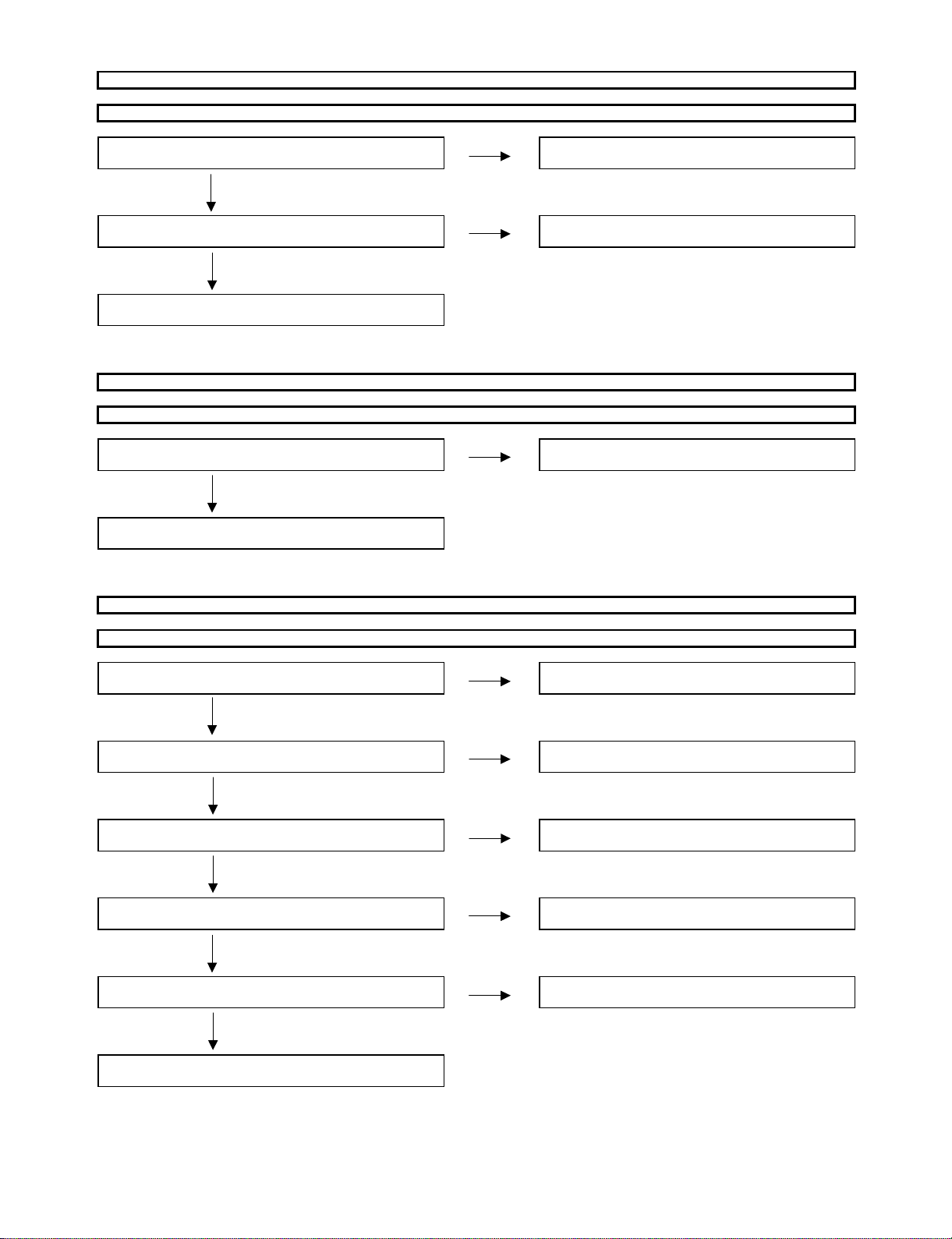
No sound from external input devices (3)
Does not the sound of the audio signal input to INPUT3 (J506) go out?
Does not the sound of the audio signal input to INPUT4 (J503) go out?
J506
Is the audio signal properly sent to pin (5) (VIN15_L) and
(7) (VIN17_R) of (COMP_1_IN) J506? that connects of J506
YES
J503
Is the audio signal properly sent to pin (5) (VIN11_L) and
(7) (VIN13_R) of (COMP_2_IN) J503? that connects of J503
YES
J506
Is the audio signal properly sent to pin (178) (VIN15_L) and
(176) (VIN17_R) of IC3001(MAIN_MICON)? (MAIN_MICON)
YES
J503
Is the audio signal properly sent to pin (181) (VIN11_L) and
(179) (VIN13_R) of IC3001(MAIN_MICON)? (MAIN_MICON)
YES
Refer to "No Sound output in all modes"
NO
Check the setting of an external input device
NO
Check the setting of an external input device
NO
Check the line between J506 and IC3001
NO
check the line between J503 and IC3001
The Audio Signal not output (5)
No audio signal output from AUDIO_OUTPUT terminal.
Is audio signal output to pin (4/R-ch) and (2/L-ch) of audio
output terminal J502
YES
Is audio signal sent to pins (25) (AOUT_R) and
(26) (AOUT_L)of IS3001 (MAIN_MICON)? (MAIN_MICON)
YES
Check IC3001 (MAIN_MICON) and its peripheral circuit
NO
Check the connection of J502 and external devices.
NO
Check the line between J502 and IC3001
6 – 3
Page 27
No picture on the display (1)
The picture doesn't appear in all modes.
LC-26/32A37M
Is the LVDS signal output from IC3001(MAIN_MICON)?
LVDS0_P/N(140/141), LVDS1_P/N(137/138),
LVDS2_P/N(134/135), LVDS3_P/N(128/129),
LVDS4_P/N(125/126), LVDS_CP/CN(131/132)
YES
Is the LVDS signal input to IC8103(LCD_CONTROL)?
A0+/-(165/164), A1+/-(167/166), A2+/-(169/168), and IC8103
A3+/-(189/188), A4+/-(191/190), ACK+/-(187/186)
YES
Is the control signal of LCD controller normal?
YES
Is VCC_3.3V, VCC_2.5V or VCC_1.5V supplied
to IC8103? _POWER_SUPPLY) and the peripheral
YES
Are the video signals BR/BG/BB (0_P/M-3_PM), FR/
FG/FB(0_P/M-3_M/P) and the CLK signals (BCLK_P/
M, FCLK_P/M) output from IC8103?
YES
Are BR/BG/BB(0_P/M-3_P/M), BCLK(P/M) input to
connector SC8201 and FR/FG/FB(0_P/M-03_P/M),
FCLK(P/M) input to connector SC8202?
NO
NO
NO
NO
NO
NO
Check IC3001 and its peripheral control circuits.
Check the line between IC3001 (MAIN_MICON)
Check the control signal R/L_LINE, U/D_OUT_LINE
FRAME_LINE, BANK_SEL_LINE, TEMP1/2/3_LINE
QS_EN_LINE, etc.
Check if IC8402(MULTI_CHANNEL_SYSTEM
power supply circuit are normal.
Check IC8103 and its peripheral circuits.
Check the line between IC8103 and CN8201/CN8202
YES
Are the gradiation signals (VH/VL_247, 191, 159, 63,
31, 0) normal sent from IC8201( GLAY_LEVEL peripheral circuits and IC8103 is normal.
_GENERATION) to CN8201/CN8202? (Each line of DAC_CLK/DATA/LATCH)
YES
Check the connectors CN8201/CN8202 and LCD Panel
NO
Check IC8201 and the communication between its
6 – 4
Page 28
LC-26/32A37M
No picture on the display (2)
Does not the picture come out when UHF/VHF is received?
Is the video signals (VIN1) output form pin (17)
of TUNER (TU201)? named TU201 and IC3001 (MAIN_MICON)
YES
Is the video signal (VIN1) sent to pin (191) of IC3001
(MAIN_MICON)?
YES
Refer to "The picture doesn't appear in all modes."
No picture on the display (3)
Does not the picture of the composite video signal input go out?
Is CVBS signal output from pin (8) in input terminal
J504 to pin (188) IC3001 (MAIN_MICON)?
NO
NO
NO
Check whether I2C is normal accessed between
Check the line between TU201 and IC3001
Check the line between J504 and IC3001
YES
Refer to "The picture doesn't appear in all modes"
No picture on the display (4)
Does not the picture of the Y/C video signal (S-video) go out?
Is Y/C signal input from pin (3)/Y and (4)/C of input
terminal J 505
YES
Is Y/C signal output from pin (3)/Y and (4)/C connect
to pin (184)/VIN7 and (187)/VIN6 of IC3001 (MAIN_MICON) (MAIN_MICON)
YES
Is the Y/C video signal detection function SV1JSW signal
from pin (6) of the input terminal J505 normal?
YES
Is the SV1JSW signal input to pin (201) of IC3001
(MAIN_MICON)?
NO
NO
NO
NO
Check the S_IN (J505) line and its peripheral circuits
Check the line between J505 and IC3001
Check J505 or peripheral circuits.
Check the line between J505 and IC3001
YES
Is Y/C signal sent to pins (184)/Y and (187)/C
of IC 3001 (MAIN_MICON)? (MAIN_MICON)
YES
Refer to "The picture doesn't appear in all modes"
NO
Check the line between J505 nad IC3001
6 – 5
Page 29

No picture on the display (5)
Does not the picture of the DVI(ANALOG) video signal input INPUT6 (15pin-D-SUB) terminal go out?
Are the video signal and the synchonized signal input from
pin (1,2,3)/(R,G,B),(13 and 14)/(V,H) of input devices
terminal D-SUB (SC2301)
YES
Is EDID data pin (6)/SCl and (5)/SDA of IC2304
(EEPROM) accessed, and is it read from pin (15), (12) of EDID data of IC2304
of a DVI terminal SC2301
YES
Are the video signal and the synchronized signal input
from pin (174, 173,172)/(R,G,B), pin (171,47)/(H,V) of
IC3001 (MAIN_MICON)?
YES
Refer to "The picture doesn't appear in all modes"
NO
NO
NO
Check the connection and setup with the external DVI
Is access possible ui the re-writing or exchange
NO
Check the circumference circuit of SC2301 and IC2304
Check the line between SC2301 and IC3001
LC-26/32A37M
No picture on the display (6)
Does not the picture of the component video signal input INPUT3 (J506) go out?
Does not the picture of the component video signal input INPUT4 (J503) go out?
Is COMPONENT video signal input to pin (3)/Y, (5)/Pb
(7)/Pr of the input J506? device.
YES
Is COMPONENT video signal input to pin (3)/Y, (5)/Pb
(7)/Pr of the input J503? device.
YES
Is COMPONENT video signal input (J506) into pin (177),
(176) and (175) of IC3001 (MAIN_MICON).
YES
Is COMPONENT video signal input (J503) into pin (180),
(179) and (181) of IC3001 (MAIN_MICON).
YES
Refer to "The picture doesn't appear in all modes"
NO
NO
NO
NO
Check the connection of J506 and the external input
Check the connection of J503 and the external input
Check the line between J506 and IC3001
Check the line between J503 and IC3001
6 – 6
Page 30

LC-26/32A37M
No picture on the display (7)
Does not the picture of the HDMI signal input to INPUT1 (SC1901) / INPUT2 (SC1921) go out?
Is the HDMI detection function output from pin (19) of Check the line between SC1901 and IC3001
the HDMI terminal (SC1901) normal? (MAIN_MICON) of pin (205)
NO
Is the HDMI detection function output from pin (19) of Check the line between SC1921 and IC3001
the HDMI terminal (SC1921) normal? (MAIN_MICON) of pin (203)
Check the connection and setup with the
external HDMI Devices
YES
Is EDID data pin (6)/SCL, pin (5)/SDA of NO Is access possible in the re-writing or exchange of
IC1902 (EEPROM) accessed, and is it read from pin EDID data of IC1902
(15), (16) of a HDMI terminal SC1901
NO
Check the circumference circuit of SC1901, IC1902 and
IC1915 (HDMI_RECEIVER)
Is EDID data pin (6)/SCL, pin (5)/SDA of NO Is access possible in the re-writing or exchange of
IC1922 (EEPROM) accessed, and is it read from pin EDID data of IC1922
(15), (16) of a HDMI terminal SC1901
NO
Check the circumference circuit of SC1901, IC1902 and
YES IC1915 (HDMI_RECEIVER)
Is TMDS signal input pin(59,58)/TMDS2_CLKP/N NO Check the line between SC1901 and IC1951
(63,62)/TMDS2_D0P/N, (67,66)/TMDS2_D1P/N
(71,70)/TMDS2_D2P/N of IC1951 from SC1901
Is TMDS signal input pin(40,39)/TMDS2_CLKP/N NO Check the line between SC1921 and IC1951
(44,43)/TMDS2_D0P/N, (48,47)/TMDS2_D1P/N
(52,51)/TMDS2_D2P/N of IC1951 from SC1921
YES
Is each signal output fron DINR[0:7], DING[0:7] NO Is the control signal of IC1951 and IC3001
DINB[0:7], pin(2,3)/HDMI_H/V, (1)/DINEN, (121)/ (MAIN_MICON) normal? (HDMI_RST etc.)
DINCK, of IC1951?
YES
Is each signal of DINR[0:7], DING[0:7], DINB[0:7], pin (171,47)/HDMI_HV, (48)/DINEN, (49)/DINCK of IC3001 (MAIN_MICON) input?
YES NO
Refer to "The picture doesn't appear in all modes." Check the line between IC1951 and IC3001
(IC1941 etc.)
6 – 7
Page 31

LC26A37M
CHAPTER 7. BLOCK DIAGRAM/OVERALL WIRING DIAGRAM
[1] BLOCK DIAGRAM
BL
LC-26/32A37M
ServiceManual
LCD
Panel
INV
block
POWER
block
13.5V
ON/OFF
OPC
10W x 2
MAIN
HDMI
HDMI
AMP
YDA148
LR
LR
PC
HDMI-Rx
SII9025
24bit
D-in
AOUT1
AOUT2 /AIN5
AIN4
AIN3
AIN2
AIN1
㪪㫆㫌㫅㪻㩷
㫄㫌㫃㫋㫀㫇㫃㪼㫏
S-IF
Flash
1MB
FONT
ROM
1024 letter
VIN 19-21 VIN 11-13
RGB
VIN 15-17
YPbPr
T-CON
䌖䌃䌔䌐䋭䌐䌲䌯
YPbPr
CVBS
LVDS
CVBS
VIN 6,7,9
Y/C
VIN 3
8051
3D-IP
3D-NR
3D-Y/C
VOUT 1
L
LED_R
E
LED_G
D
R/C
LED
IR
U
N
LED_OPC
OPC
I
䌓䌬䌯䌷
䌁/䌄
KEY
EEPROM
Buffer
CN
8KByte
BR24L64F
I2C_BUS
VIN 1VIN5 VIN2
CVBS
OPC
IR PASS
TC7W00U
RS232CTxRx
ISL83220
RS232C
T
K
E
Y
U
N
I
T
Option
CH+
CHVol䋫
VolMENU
INPUT
POWER
L R
Tuner
SAW
LR䋨COMP䋩
S-IF
Demodulation
Y
Pb
Pr
7 – 1
L
R
Pb
LR䋨COMP䋩
Y
Pr
L
R
LR䋨CVBS䋩
CVBS
L R
(ctrl䋩
RESET
V
VS
L R
LR䋨CVBS/䌓䋩
CVBS
䋨TUNER䋩
D/A_SEL
D_POW
ANT_POW
SIO
AGC
AFT
GPIO
I2C
Page 32

LC-26/32A37M
[2] OVERALL WIRING DIAGRAM
7 – 2
Page 33

LC26A37M
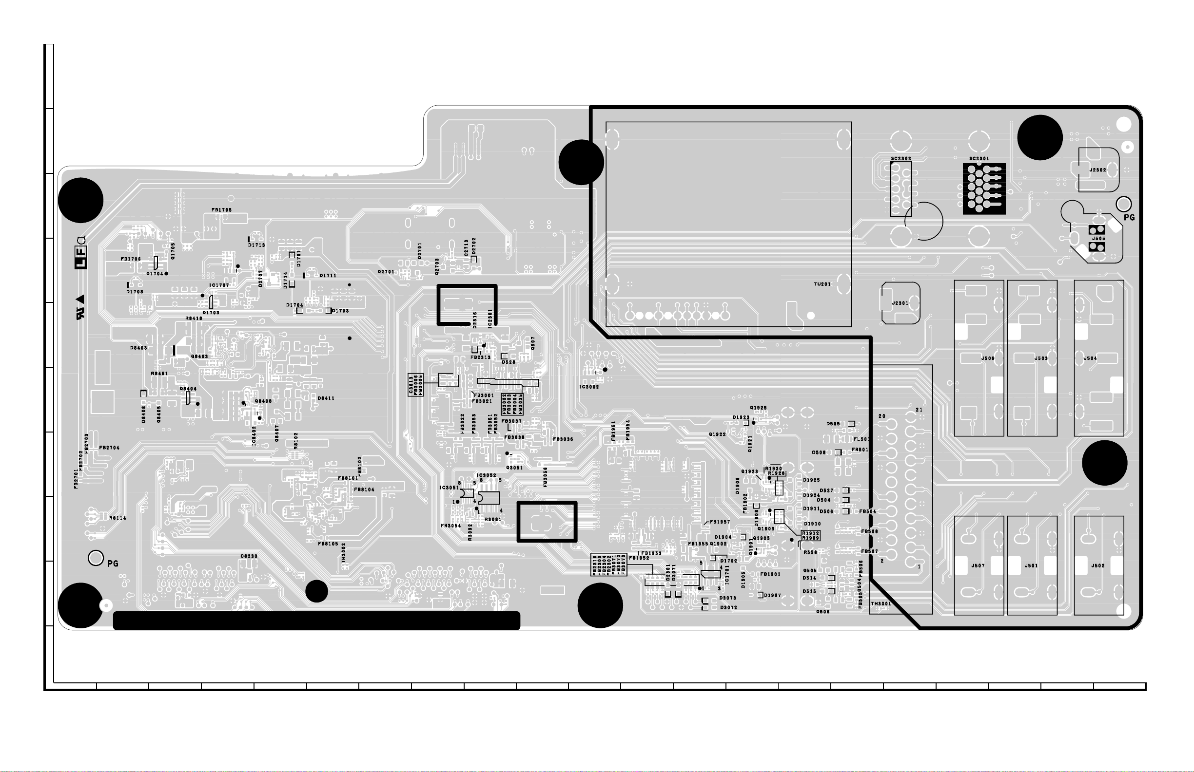
CHAPTER 8. PRINTED WIRING BOARD
[1] MAIN UNIT
MAIN Unit Side-A
J
I
H
LC-26/32A37M
ServiceManual
G
F
E
D
C
B
A
123456789
10 11 12 13 14 15 16 17 18 19 20 21
8 – 1
Page 34

LC-26/32A37M
MAIN Unit Chip Side-A
J
R2336R2337
I
D2319
H
G
D521
R549
C573
F
E
R575
R514
C521
Q501
C517
R525
R513
R512
Q503
C522
LUG1701
R518
R526
C525
R576
R520
Q502
C526
C524
D
R516
D2318
D2317
C555
D516
C554
D517
D518
R554
C553
FL509
R543
C556
FB509
R578
C557
R545
R544
C564
C565
R547
R546
C559
R579
FB510
C558
R521
C2317
C560
D520
C520
C562
C563
R523
R2315
C2319
R571
C581
C2320
FL510
FL511
IC2302
C502
FB502
LUG1706
C2318
R2334
C2321
R548
FL507
R532
C534
C537
R504
R503
R2314
R2331
R2330
R2335
R2311
C2322
R2316
R2317
C561
R2321
C2323
C572
IC2303
D519
FL508
R536
C541
D511D512
C507 C508
C514
R505
R506
D507
FB503
C501
R508
FB2311
D2310
FB2310
D2308
D2312
D2306
FB2308
D2304
R2320
R507
C515
FB2309
C532
D509
R2322
D2313
C570
C575
FB511
Q2303
FL513
R552
C567
R563
R567
R2333
D523
C577
R565
C579
D525
D522
C574
FB512
FL514
R553
C568
R562
R566
C
B
IC2304
C576
R564
C578
C569
D526
VA2302
R2312
R2313
VA2301
D524
D513
C552
C544
C519
C511
C512
C513
FL512
C566
C533
FL506
C529
R550
C527
D510
R509
FL502
R519
FL503
D501
D502
FL504
R522
R524
FL505
D503
FL2303
R2308
FL2302
R2307
FL2301
R2306
D2302
R551
R531
R577
L501
IC501
R515
C504
C505
C506
D2311
C2312
FB2306
FB2307
D2305
C571
C545
C2310C2311
D2303
C2325
D2309
FB2315
R2324
R2325
R2703
FB2312
R2302
D2307
FB2305
C2324 R1745
FB2314
R2323
R2326
C2327
R2327
C2326
R2328
C2331
D2314
C2330
D2315
C206
C201
SC1921
SC1901
C202
R214
Q1906
C1922
C1906
L202
D1922
D1921
IC1922
IC1902
D1903
D1902
C207
R3010
R209
R213
C208
R210
Q203
R206
R215
R1976
C2004
C2002
R1761
C203
FB1956
Q1701
R205
C204
R1759
R1760
R208
R211
R1926
R212
Q202
R1907
C1753
C1752
C2302 C2303
P2301
R3056
R1971
C1993
R207
C209
C1995
FB2301
C205
IC1951
C1974
C1973
R1965
FL1901
C1977
R1966
C1971
C1972
R1963
R1964
R1962
R1960
IC1941
P3091
R1951
C210
C1941
R1957
R1956
R1955
R1954
R1953
R1952
LUG1704
Q2704
R2720
C2707
R2722
R2719
C2747
C2731
C2743
C2744
C2745
C2749
R2724
R2701
L2705
C2742
R2725
C2750
C2751
C3036
D2708
C2753
C2752
C2760
IC2702
C2762
C2758
C2756
C2754
P2702
C2764
C2755
C2763
C2761
R2726R2727
R2738
C2757
D2709
L2706
R2735
R2733
R2734
C2759
P3081
R2736
C3054
R3094
C2720
D2705
C2732
R3093
X3051
C2736
C2740
C2728
C2735
IC3001
C2721
D2706
C3055
C2726
C2738
R3054
P2701
L2704
L2701
C2723
C2737
C2741
R8104
C2739
R8120
R2728
R2721
C2727
C2724
C2718
C2714
R2723
C2708
R2706
R2737
C2765
C2705
C3083
R3003
IC2701
C2715
C2711
Q2702
C2701
R8130R8131R8132R8134R8135
R2730
C2729
C2712
C2709
C2702
R3009
R3013
R3016
R3018
R2729
C2706
C2704
R2732
R2711
C2730
R2716
C2725
C2717
R2715
R2731
C8232
L2703
L2702
FL8101
R8121
R8115
R8266
D2703
C2722
C2733
C2734
FB8106
C8102
IC8102
C2719
R2702
C8229
D2704
L1702
C8228
R8149
R8142
R8143
R8263
C2746
C2748
D1710
R8246
R8146
R8147
C8417
R8145
R8425
D8401
C8406
C8405
C8103
IC8103
IC1704
C8467
C8129
R8463
R8462
L1703
C8468
C2710
L8401
R8405
R8404
C1735
C1741
C1737
C1733
C8404
R8108
R8408
R8406
D8404
Q8406
C8456
R8401
C1734
FB1702
C8407
C8408
D1712
R8243
D8402
C8415
R8410
C8423
C8450
C8449
R8118
C2716
R1737
C8451
R8245
D8407
D8406
IC8101
R8248
C8418
R8244
IC1706
C8225C8226
C8234
R8427
C8420
C8101
R8148
R8472
C8444
C8443
R8105
R2704
IC8404
R8439
C8434
R8441
R8106
C1751
C1744
D1709
R8428
R8437 R8438
IC1703
R8237
C1746
C8428
R8250
R8435
C8460
C8461
C8208
R8249
R8210
R8215
R8213
R8242
C1742
D8405
C8433
C8466
R8225
C8212
R1736
R8414
IC8202
R8433
R8222
C8213
FB1703
C1725
R8419
R8421
R8420
C8438
D8410
L8402
R8211
R8218
R8217
R8103
C1747
R1735
C8203
C8223
R8101
C8441
C8206
C8222
FB1704
R1747
L8403
CN8201CN8202
R8403
R1746
L1701
D8409
IC8201
D1706
P1701
R8458
C8453
C8454
C8458
R8207
R8202
R1703
R8220
R8201
C8219
R1749
C8238
C8239
R8122R8123R8124R8125R8127R8128R8129
D1707
D1705
R8204
R8208
R8212
R8214
R8219
R8221
R8206
R8226
R8228
R8233
C8204
C8207
C8209
C8215
C8211
C8214
C8210
C8216
C8217
R1748
C1750
C1721
IC1702
R1750
R8265
C1729
FB1701
C1720
C1724
C2766
C2767
C2768
C2769
C8202
C8218
LUG1705
P2703
P8102
LUG1702LUG1703
A
123456789
10 11 12 13 14 15 16 17 18 19 20 21
8 – 2
Page 35
MAIN Unit Side-B
J
I
H
G
LC-26/32A37M
F
E
D
C
B
A
123456789
10 11 12 13 14 15 16 17 18 19 20 21
8 – 3
Page 36

LC-26/32A37M
MAIN Unit Chip Side-B
J
I
H
G
R1751
C1748
R1753
R1733
C1705
C1716
R1752
FB1706
C1715
D1708
R1728
C1722
C1712
R1715
R1762
R1713
C1749
R1710
R1739
Q1704
R1709
R1708
Q1705
R1738
C1702
C1711
R1742
R1743
R1741
R1740
C1710
C1709
R1706
R1705
Q1703
R1707
FB1705
R1758
R1757
R1756
R1754
C1743
R1734
R1755
IC1707
C1745
C1728
R1716
C1719
R1727
C1740
R1725
C1736
C1738
R1732
R2718
R2739
R1722
C1739
D1713
R1730
R1729
C1718
D2707
R1721
R1720
R1719
R2705
R2740
C1727
C1726
D1701
R1744
D1714
R1701
C1723
D1704
C1732
R1718
C1731
D1711
C1730
R1724
R1702
R1723
R1714
R1712
R1711
D1703
C1713
C1717
C1714
Q2701
C2703
R2707
R2708
R2709
D2701
R2710
R2712
Q2703
R2717
R2713
R2714
C2713
D2702
R8418
D8408
R8223
R8460
C8410
R8430
C8409
D8403
R8461
Q8405
R8216
F
E
FB2703
FB2704
FB2702
D
FB2701
R8114
R8205
C8205
R8241
C8221
R8240
R8417
C8447
R8203
R8238
R8239
C8201
C8455
R8236
R8224
R8232
R8459
R8235
C8220
Q8404
C8439
R8449
R8450
C8459
R8453
R8454
C
B
C8224
C8440
R8447
R8429
C8422
R8409
Q8403
R8432
C8448
R8455
R8444
C8445
R8456
C8435
R8452
R8451
R8442
C8437
C8462
C8465
C8463
C8442
R8446
C8446
R8448
R8431
R8445
C8235
R8467
R8474
R8469
C8230
Q8408
IC8402
R8471
R8470
R8468
R8413
R8411
C8413
C8424
C8464
C8457
C8411
R8416
R8415
R8412
C8402
R8424
C8421
R8422
R8426
R8423
C8452
Q8407
R8113
C8131
C8432
C8401
R8464
R8465
R8466
R8116
C8126
R8102
C8122
R8119
R8247
C8135
C8132
C8125
R8110
R8111
R8264
C8412
C8430
C8130
C8403
D8411
R8107
C8117
C8123
C8128
C8127
C8429
R8109
R8112
C8118
C8124
C8107
C8121
R8402
R8440
C8112
C8116
C8109
C8115
C8120
FB8105
C8137
C8110
C8108
C8119
C8139
C8114
C8106
C8105
C8113
C8111
FB8101
FB8104
R8117
C8133
TH3002
C3048
C8104
FB8102
C8134
C8141
C8233
C3014
C3021 C3022
C3017
R3006
R3004
C3023
R3007
C3024
C8227
C3013
FB3006
C3047
C3018
C3026
C2301
R2332
IC2301
D2316
FB2313
R2301
R2303
R2304
C3016
C3003
FB3001
R3095
FB3021
R3023
C3057
IC3051
C3060
FB3054
R3092
FB3053
C3020
C3052
C3009
R3030
C3081
R3081
C3082
C3005
FB3002
R3020
R3028
C3058
C3056
C3027
IC3052
R3011
C3032C3033R8407
FB3051
C8237
C3010
C3011 C3012
C3006
C3034
FB3005
C3025
FB3022
R3024
C3051
R3075
R3076
R3074
R3071
R3072
R3073
FB3052
C3059
C3053
C3007
FB3003
R3021
R3029
R574
C8236
D528
C8231
R530
C3015
C3008
FB3004
R3022
R3026
FB3037
Q3051
Q507
R3012
FB3038
R3027
R568
C3045
R533
C3046
FB3035
C3038
C3043
C3028
R3002
R3001
C3031
C3037
C3039
C3040 C3041
C3029
C3030
C3044
FB3056
R3017
C3042
FB3036
R3025
R3031
C3004
IC3002
C3035
C3001
C3002
FB1951
R1972
R1961
C1969
C1952
C1907
C1960
R1958
C1908
R1959
FB1954
C1978
C1958
C1955C1956C1957
C1954
R1975
C1968
C1970
C1966
C1967
C1959
C1965
C1964
C1961 C1962
FB1952
FB1953
R1973
R2309
C1975
C1976
C1979
R1974
R2305
FB2316
C2304
C1980
FB2303
C2308
C1982
C1983
C1981
C1984
FB2302
FB2304
C2306
C2309
C1989
C1987
C1988
C1985
C1986
R1968
D2301
C1991
C1990
C1994
C1992
R1969
R1970
C1996
C1997
C3075
C3076
D3071
C1998
C1999
C2011
C2012
C1963
FB1955
C2001
C2000
C1701
FB3071
C3073
C2018
C2014C2015C2016
C2009C2010
C2008
C2006
C1703
C3074
FB3072
FB3073
C3071
C3072
C2017
C2013
C2007
C2005
FB1957
D1702
C1704
R1977
D3073
D3072
C1708
IC1701
C1707
C1706
R1704
R1924
Q1922
R1905
R1906
Q1902
C1905
D1904
D1923
Q1921
R1925
R1904
Q1901
D1905
R1921
D1906
FB1902
Q1925
D1908
FB1901
C1903
C1901
D1907
Q1905
R1914
R1922
R1932
C1921
Q1923
C1902
Q1903
R1923
R1902
R1903
C1904
R1930
R1928
R1933
R1912
R1909
R1915
D1924D1925
D1911
D1910
C580
R558
Q506
Q505
D514
R542
D515
R511
C516
D508
R541
R510
R517
D527
D504
R501 R502
D506
C548
R537
C549
R538
C550
C535
C536
C551
D505
C509
FL501
FB501
C542 C543
R539
Q504
R540
R534
R535
R527 R528
C518
R529
C510
FB504
C538
C539
C503
C530 C531
FB505FB506
FB507FB508
C3019
TH3001
A
123456789
10 11 12 13 14 15 16 17 18 19 20 21
8 – 4
Page 37

[2] R/C, LED/KEY UNIT
R/C, LED Unit Side-A R/C, LED Unit Side-B
J
I
R/C, LED Unit Chip Side-A R/C, LED Unit Chip Side-B
H
LC-26/32A37M
G
F
E
D
KEY Unit
C106
C105
C104
IC101
D116
R135
R136
D103
R105
R110
R104
R108
R109
R107
Q102Q103
R137
Q104
R117
R102
Q105
R106
R138
P101
R132
R101
C102D101
C
B
A
123456789
10 11 12 13 14 15 16 17 18 19 20 21
8 – 5
Page 38

LC-26/32A37M
[3] POWER UNIT
POWER Unit Side-A
J
I
H
G
F
E
D
C
B
A
123456789
10 11 12 13 14 15 16 17 18 19 20 21
8 – 6
Page 39

POWER Unit Side-B
J
I
H
G
LC-26/32A37M
F
E
D
C
B
A
123456789
10 11 12 13 14 15 16 17 18 19 20 21
8 – 7
Page 40

LC-26/32A37M
POWER Unit Chip Side-B
J
I
H
TL7002
G
TL7003
TL7004
F
E
TL7205
R7235
R7230
D7220
R7223
C7224
Q7205
D7218
R7243
R7236
TL7217
TL7212
C7217
C7230
TL7207
TL7214
TL7220 TL7209 TL7210
R7239
R7266
R7241
TL7215
R7240
R7234
R7237
RJ1
TL7206TL7208
TL7213TL7211
R7273
D7233D7232
Q7210
R7276
TL7219
R7279 R7278
R7277
R7233
R7259 R7224
R7229
TL7216
D7228
C7219
D7219
R7242
R7245
D7231
D7230
R7260
R7244
R7232
D7221
TL7221
R7246
R7124
D7103
C7107
D7105
TL7103
C7115
C7101
D7106
FB7106
R7133
FB7101
IC7101
D7110
R7102
C7105
TL7105
R7103
C7109
R7101
C7102
FB7105
R7110
R7112
TL7106
TL7107
TL7102
C7211
TL7101
R7206
R7207
C7203
D7205
D7216
FB7201
C7231
R7261
R7208
Q7203
D7209
D7229
R7219
TL7201
D7207
R7231
D7223
C7206
R7257
C7215
D7204
R7238
Q7208
D7225
D7203 D7226
Q7201
R7209
RJ2
R7264
R7212
R7265 R7258
R7269
TL7203
R7129
R7131
R7135
R7111
R7114
R7123
TL70012
TL70013TL70014TL7001
TL70011
R7128
R7127
R7126
R7125
C7106
R7136
R7117
R7130
D7108
Q7104
Q7102
R7134
R7263
D7208
D7222
R7262
Q7206
C7229
R7249
TL7204
C7204
Q7202
R7222
R7213
Q7207
R7225
R7226
Q7209
R7227
C7214
R7228
C7226
R7248
D7114
RJ3
TL7218
R7247
R7250
R7251
TL7202
R7256
R7255
D7210
R7271
R7221 R7268
R7220 R7267 D7211
D
R7204
C
R7205
R7203
R7202
R7106
R7201
TL7108
TL7111 TL7112
R7107 R7105
R7109 R7108
B
A
123456789
Q7101
R7120
D7109
R7121 R7118
R7281 R7280
R7253 R7252
D7107
TL7104
FB7107 R7116 R7119 R7115
R7132
R7254
TL7224
TL7222
TL7223
LF1
C7225
10 11 12 13 14 15 16 17 18 19 20 21
8 – 8
Page 41

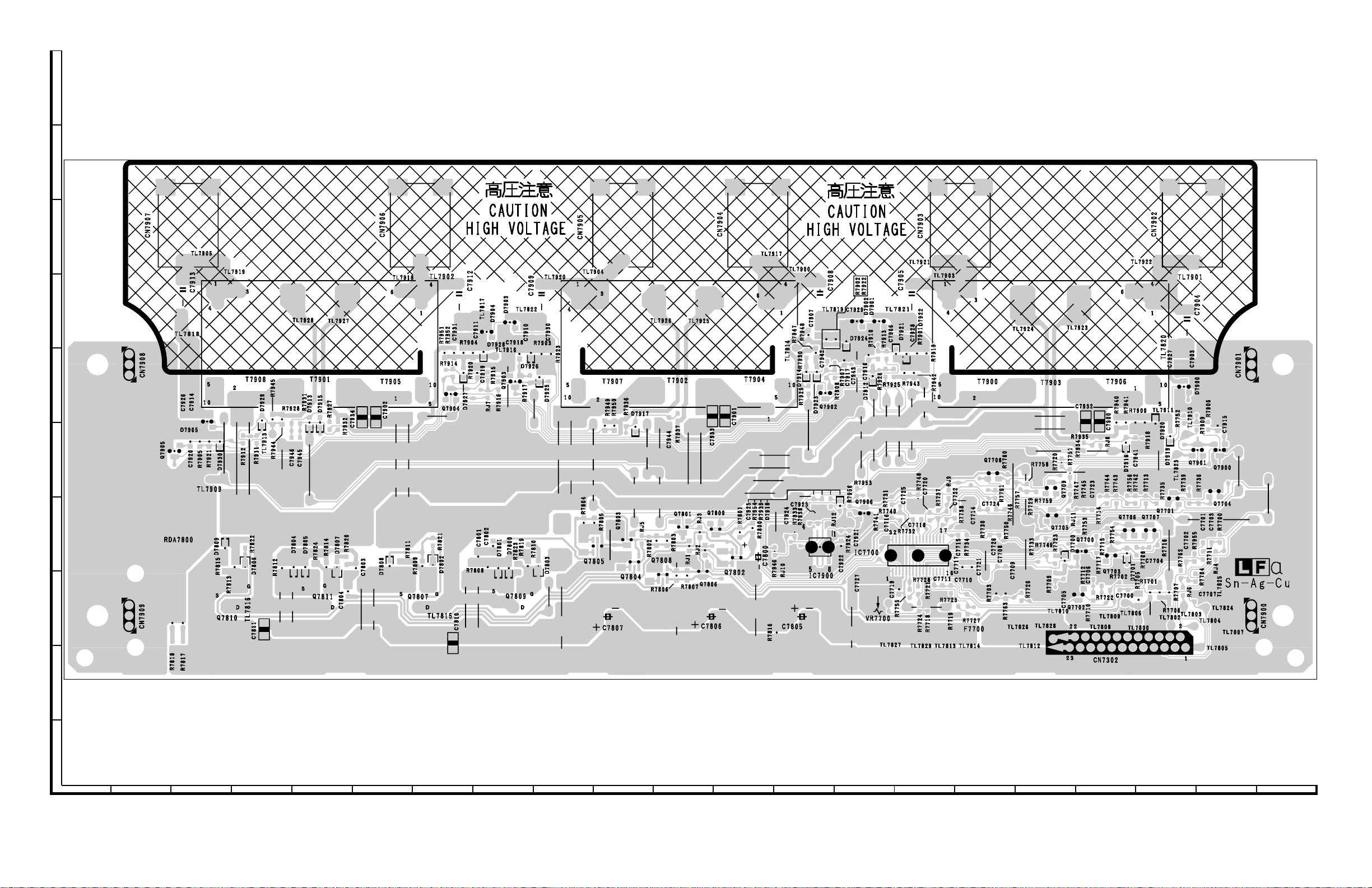
[4] INVERTER UNIT
INVERTER Unit Side-A (LC-26A37M)
J
I
H
G
LC-26/32A37M
F
E
D
C
B
A
123456789
10 11 12 13 14 15 16 17 18 19 20 21
8 – 9
Page 42

LC-26/32A37M
INVERTER Unit Chip Side-B (LC-26A37M)
J
I
H
G
C7914
C7926
R7921
R7905
R7915
C7920
Q7904
D7809
R7912
R7815
R7911
R7813
D7930
R7944
R7822
D7929
R7945
D7806
C7810
R7812
D7804
D7805
R7824
R7814
C7946
D7913
R7928
C7945
R7927
R7820
D7807
R7931
C7803
C7804
RJ33
R7932
C7943
D7915
R7925
RJ32
R7926
D7912
R7811
R7821
D7808
R7809
D7802
C7801 C7802
C7811
D7905
Q7905
C7919
F
R7914
E
C7808
C7809
D
R7817
R7818
R7808
C7934
C7902
D7801
R7904
D7800
R7920
R7952
C7911
R7823
D7928
R7951
R7819
R7810
C7931
D7927
D7904
C7918
R7917
R7916
D7803
RJ26
RJ29
Q7903
Q7902
Q7804
D7903
C7917
C7910
D7926
D7925
R7907
R7908
R7923
R7903
R7803
R7950
C7944
C7930
R7802
R7949
R7936
D7917
Q7801
R7937
RJ19
RJ20
R7806
R7807
Q7808
Q7806
RJ24
RJ22
RJ21
R7816
C7933
C7901
Q7802
RJ27
R7801
R7800
Q7800
R7804
R7946
R7805
D7923
C7923
R7933
C7929
R7947
R7938
C7924
R7902
Q7805
R7922
R7948
RJ18
C7907
IC7900
D7924
RJ17
Q7803
D7902
C7925
RJ16
R7924
C7922
R7954
C7916
C7921
R7741
D7901
R7953
Q7906
RJ15
R7910
C7727
D7922
R7913
R7939
R7956
C7716
D7918
R7718
R7901
D7921
R7740
R7724
C7906
R7919
R7732
RJ14
C7928
R7943
C7718
C7719
R7942
R7755
IC7700
R7728
R7731
C7720
RJ13
R7737
RJ12
R7721
C7722
R7719
R7761
C7711
R7738
C7715
R7725
R7734
R7727
Q7705
C7725
C7721
C7710
R7747
R7748
C7717
R7722
C7714
RJ11
C7708
R7730
C7709
C7723
RJ10
RJ9
R7703
R7745
C7726
Q7708
R7746
R7750
R7763
C7724
C7932
C7900
R7760
R7757
R7729
R7758
R7749
R7759
R7733
R7723
Q7700
D7700
Q7709
R7714
R7709
R7712
C7705
R7715
R7754
Q7703
D7920
R7940 R7941
R7900
C7942
R7929
R7934
R7935
Q7706 Q7707
R7708
D7701
R7726
R7701
R7705
D7914
C7704
R7706
C7903
R7918
R7930
R7751
C7927
D7916
R7720
RJ6
R7716
Q7702
R7707
RJ8
C7941
RJ5
R7717
D7900
RJ7
D7919
R7735
C7706
R7710
R7753
R7756
R7744
R7702
C7915
R7752
Q7900
R7909
R7906
Q7901
R7742
Q7701
R7736
R7739
R7713
R7743
Q7704
RJ4
RJ3
C7700
C7702
R7955
R7711
RJ2
C7701
C7703
R7700
R7704
RJ1
R7762
C7707
C
B
A
123456789
10 11 12 13 14 15 16 17 18 19 20 21
8 – 10
Page 43

INVERTER Unit Side-A (LC-32A37M)
J
I
H
G
LC-26/32A37M
F
E
D
C
B
A
123456789
10 11 12 13 14 15 16 17 18 19 20 21
8 – 11
Page 44
LC-26/32A37M
INVERTER Unit Side-B (LC-32A37M)
J
I
H
G
F
E
D
C
B
A
123456789
10 11 12 13 14 15 16 17 18 19 20 21
8 – 12
Page 45

INVERTER Unit Chip Side-B (LC-32A37M)
J
I
H
LC-26/32A37M
G
D7903
D7800
Q7903
C7918
R7823
R7917
R7819
R7810
C7910
D7926
C7930
R7903
D7925
D7803
R7923
R7804
R7805
Q7805
R7949
R7950
R7936
Q7803
D7917
Q7804
R7948
R7930
D7914
R7929
C7901
Q7801
RJ1
R7807
RJ3
Q7806
C7933
R7800
R7801
Q7800
RJ2
Q7802
R7946
RJ10
C7924
R7933
R7937
C7944
R7802
R7803
RJ5
R7806
Q7808
C7931
C7911
D7904
D7928
R7904
R7951
R7952
R7920
C7919
R7914
D7927
R7915
C7801
RJ7
R7808
R7916
C7802
D7801
F
C7934
R7820
C7804
C7803
C7902
D7808
R7811
C7926
C7914
D7905
R7921
D7930
D7809
R7815
R7813
R7912
R7822
D7806
R7905
C7920
E
Q7905
D
R7911
D7929
R7945
R7944
R7812
R7928
C7946
D7804
R7931
C7945
D7805
D7913
R7824
D7915
R7927
R7814
R7932
D7807
R7809
Q7904
R7821
D7802
C
C7808
C7809
R7818
R7817
C7811
C7810
R7816
R7938
C7907
R7947
D7923
C7925
IC7900
C7923
Q7902
R7954
R7902
C7942
R7907
RJ12
R7908
R7939
R7922
C7929
D7918
R7924
C7922
D7924
C7917
R7956
C7921
D7902
C7943
R7953
Q7906
C7727
C7916
D7912
D7901
R7910
R7741
R7913
R7926
R7925
R7731
C7716
C7906
D7921
R7740
C7719
C7928
D7922
R7943
C7725
R7755
R7942
R7732
IC7700
R7901
R7748
R7728
R7724
C7718
R7919
R7718
C7720
R7721
R7737
C7711
RJ9
C7722
R7725
R7738
C7715
R7719
C7717
R7734
C7710
R7727
C7721
C7714
Q7708
R7730
C7726
R7761
C7724
C7708
R7703
R7750
R7760
R7746
C7709
R7763
R7757
R7726
R7758
R7759
R7729
R7733
Q7709
R7749
Q7705
R7723
R7709
R7720
D7700
C7705
RJ11
R7751
R7747
R7753
Q7700
R7712
Q7702
C7932
R7934
R7745
R7935
C7723
C7706
R7710
C7900
R7714
R7715
RJ8
R7717
R7744
R7754
Q7703
R7722
R7940
R7941
D7916
R7756
R7743
Q7706 Q7707
D7701
R7702
C7700
R7900
C7941
R7742
R7708
R7705
R7918
R7713
C7704
R7701
D7920
R7735
R7716
R7706
D7919
Q7701
R7707
C7927
D7900
R7762
RJ6
C7903
R7752
C7702
R7739
R7909
Q7901
R7955
R7704
C7707
R7736
C7701
R7711
R7906
C7703
C7915
Q7900
Q7704
R7700
RJ4
B
A
123456789
10 11 12 13 14 15 16 17 18 19 20 21
8 – 13
Page 46

LC-26/32A37M
LC26A37M
CHAPTER 9. SCHEMATIC DIAGRAM
[1] SCHEMATIC DIAGRAM
1. Description of Schematic Diagram
ServiceManual
9 – 1
Page 47

2. MAIN Unit-1
J
I
H
G
LC-26/32A37M
AND SHADED COMPONENTS=SAFETY RELATED PARTS
F
E
D
C
B
A
123456789
10 11 12 13 14 15 16 17 18 19 20 21
9 – 2
Page 48

LC-26/32A37M
3. MAIN Unit-2
J
I
H
G
F
E
D
C
B
A
123456789
10 11 12 13 14 15 16 17 18 19 20 21
9 – 3
Page 49

4. MAIN Unit-3
J
I
H
G
LC-26/32A37M
F
E
D
C
B
A
123456789
10 11 12 13 14 15 16 17 18 19 20 21
9 – 4
Page 50

LC-26/32A37M
5. MAIN Unit-4
J
I
H
G
F
E
D
C
B
A
123456789
10 11 12 13 14 15 16 17 18 19 20 21
9 – 5
Page 51

6. MAIN Unit-5
J
I
H
G
LC-26/32A37M
F
E
D
C
B
A
123456789
10 11 12 13 14 15 16 17 18 19 20 21
9 – 6
Page 52

LC-26/32A37M
7. MAIN Unit-6
J
I
H
G
F
E
D
C
B
A
123456789
10 11 12 13 14 15 16 17 18 19 20 21
9 – 7
Page 53

8. MAIN Unit-7
J
I
H
G
LC-26/32A37M
F
E
D
C
B
A
123456789
10 11 12 13 14 15 16 17 18 19 20 21
9 – 8
Page 54

LC-26/32A37M
9. MAIN Unit-8
J
I
H
G
F
E
D
C
B
A
123456789
10 11 12 13 14 15 16 17 18 19 20 21
9 – 9
Page 55

10. MAIN Unit-9
J
I
H
G
LC-26/32A37M
F
E
D
C
B
A
123456789
10 11 12 13 14 15 16 17 18 19 20 21
9 – 10
Page 56

LC-26/32A37M
11. MAIN Unit-10
J
I
H
G
F
E
D
C
B
A
123456789
10 11 12 13 14 15 16 17 18 19 20 21
9 – 11
Page 57

12. R/C, LED Unit
J
I
H
G
LC-26/32A37M
F
E
D
C
B
A
123456789
10 11 12 13 14 15 16 17 18 19 20 21
9 – 12
Page 58

LC-26/32A37M
13. KEY Unit
J
I
H
G
F
E
D
C
B
A
123456789
10 11 12 13 14 15 16 17 18 19 20 21
9 – 13
Page 59

14. POWER Unit
J
I
H
G
LC-26/32A37M
AND SHADED COMPONENTS=SAFETY RELATED PARTS
F
E
D
C
B
A
123456789
10 11 12 13 14 15 16 17 18 19 20 21
9 – 14
Page 60

LC-26/32A37M
15. INVERTER Unit (LC-26A37M)
J
I
H
G
AND SHADED COMPONENTS=SAFETY RELATED PARTS
F
E
D
C
B
A
123456789
10 11 12 13 14 15 16 17 18 19 20 21
9 – 15
Page 61

16. INVERTER Unit (LC-32A37M)
J
I
H
G
LC-26/32A37M
AND SHADED COMPONENTS=SAFETY RELATED PARTS
F
E
D
C
B
A
123456789
10 11 12 13 14 15 16 17 18 19 20 21
9 – 16
Page 62

LC-26/32A37M
9 – 17
Page 63

PartsGuide
LC-26/32A37M
PARTS GUIDE
No. SY8U6LC32A37M
LCD COLOR TELEVISION
LC-26A37M
Note:
The reference numbers on the PWB
are arranged in alphabetical order.
[1] PRINTED WIRING BOARD
ASSEMBLIES
[2] LCD PANEL
[3] DUNTKF063FM04 (LC-26A37M)/
FM03 (LC-32A37M) (POWER Unit)
[4] DUNTKF067FM04 (LC-26A37M)/
FM05 (LC-32A37M) (MAIN Unit)
[5] DUNTKF068FM01 (R/C, LED Unit)
[6] DUNTKF069FM01 (KEY Unit)
MODELS
CONTENTS
[10] LCD PANEL MODULE (LC-
[11] CABINET PARTS (LC-32A37M)
[12] LCD PANEL MODULE (LC-
[13] SUPPLIED ACCESSORIES
[14] PACKING PARTS (NOT
LC-32A37M
[9] CABINET PARTS (LC-26A37M)
26A37M)
32A37M)
REPLACEMENT ITEM)
[7] DUNTKF070FM01 (LC-26A37M)
(INVERTER Unit)
[8] DUNTKF071FM01 (LC-32A37M)
(INVERTER Unit)
Parts marked with " " are important for maintaining the safety of the set. Be sure to replace these
parts with specified ones for maintaining the safety and performance of the set.
[15] SERVICE JIG (USE FOR
SERVICING)
INDEX
This document has been published to be used
for after sales service only.
The contents are subject to change without notice.
Page 64

LC-26/32A37M
NO. PARTS CODE
PRICE
RANK
NEW
MARK
PART
DELIVERY
[1] PRINTED WIRING BOARD ASSEMBLIES
N DUNTKF063FM04 BL N V POWER Unit (LC-26A37M)
N DUNTKF063FM03 BL N V POWER Unit (LC-32A37M)
N DUNTKF067FM04 BW N V MAIN Unit (LC-26A37M)
N DUNTKF067FM05 BW N V MAIN Unit (LC-32A37M)
N DUNTKF068FM01 AK N V R/C, LED Unit
N DUNTKF069FM01 AG V KEY Unit
N DUNTKF070FM01 BG V INVERTER Unit (LC-26A37M)
N DUNTKF071FM01 BG N V INVERTER Unit (LC-32A37M)
N RUNTKA549WJZZ AR V GND PWB Unit (LC-26A37M)
N RUNTKA550WJZZ AR V GND PWB Unit (LC-32A37M)
[2] LCD PANEL
N R1LK255T3GW40W CM N V 26"LCD Panel Module (LC-26A37M)
N R1LK315T3GW40W CN N V 32"LCD Panel Module (LC-32A37M)
[3] DUNTKF063FM04 (LC-26A37M)/FM03 (LC-32A37M) (POWER Unit)
C7002 RC-FZA562WJZZ AC V Capacitor
!
C7011 RC-KZA550WJZZ AC V Capacitor
!
C7021 RC-FZA560WJZZ AC V Capacitor
!
C7024 RC-KZA550WJZZ AC V Capacitor
!
C7027 RC-KZA550WJZZ AC V Capacitor
!
C7101 VCKYCY1CB224KY AB V 0.22 50V Ceramic
C7102 VCCCCY1HH122JY AA V 1200p 50V Ceramic
C7105 VCKYCY1HB104KY AA J 0.1 50V Ceramic
C7106 VCKYCY1HB471KY AA J 470p 50V Ceramic
C7108 RC-FZA358WJZZ AF V Capacitor
!
C7109 VCKYTV1HB102KY AA J 1000p 50V Ceramic
C7110 RC-KZA304WJZZ+ AC V Capacitor
C7111 RC-KZA304WJZZ+ AC V Capacitor
C7112 RC-EZB586WJZZ AM V Capacitor
C7113 RC-EZB294WJZZ+ AB V Capacitor
C7114 RC-FZA358WJZZ AF V Capacitor
!
C7201 RC-EZB326WJZZ+ AB V Capacitor
C7202 RC-EZB325WJZZ+ AB V Capacitor
C7203 VCKYTV1EB474KY AC J 0.47 25V Ceramic
C7204 VCKYCY1EB104KY AB J 0.1 25V Ceramic
C7206 VCKYTV1HB103KY AA J 0.01 50V Ceramic
C7207 RC-EZB593WJZZ+ AC V Capacitor
C7208 RC-KZA304WJZZ+ AC V Capacitor
C7209 RC-EZB294WJZZ+ AB V Capacitor
C7210 RC-FZA564WJZZ AD N V Capacitor
C7211 VCKYCY1HB102KY AA J 1000p 50V Ceramic
C7212 RC-KZA498WJZZ AB V Capacitor
!
C7213 RC-KZA498WJZZ AB V Capacitor
!
C7214 VCKYCY1EB104KY AB J 0.1 25V Ceramic
C7215 VCKYCY1HB104KY AA J 0.1 50V Ceramic
C7217 VCKYTV1EB104KY AB J 0.1 25V Ceramic
C7218 RC-KZA267WJZZ+ AC J Capacitor
C7219 VCKYCY1EB104KY AB J 0.1 25V Ceramic
C7220 RC-EZA480WJZZ+ AD V Capacitor
C7221 RC-EZB539WJZZ+ AE V Capacitor
C7222 RC-EZA480WJZZ+ AD V Capacitor
C7223 RC-EZB539WJZZ+ AE V Capacitor
C7224 VCKYCY1HB104KY AA J 0.1 50V Ceramic
C7225 VCKYCY1EB104KY AB J 0.1 25V Ceramic
C7226 VCKYCY1HB104KY AA J 0.1 50V Ceramic
C7227 RC-EZB294WJZZ+ AB V Capacitor
C7228 RC-EZA480WJZZ+ AD V Capacitor
C7229 VCKYCY1HB102KY AA J 1000p 50V Ceramic
C7231 RC-KZA733WJZZY AC N V Capacitor
CN7001 QEARPA210WJQZ+ AB J GROUND-PART
CN7002 QEARPA210WJQZ+ AB J GROUND-PART
CN7003 QEARPA210WJQZ+ AB J GROUND-PART
CN7004 QEARPA210WJQZ+ AB J GROUND-PART
D7103 VHDMA111G++-1Y AA J MA2J1110GL
D7104 RH-DXA068WJZZS AE J D3SB60-7000
!
D7105 VHDMA111G++-1Y AA J MA2J1110GL
D7106 VHDLI114+++-1Y AC J LI114
D7108 RH-EXA359WJZZY AE J PTZTE2533B
D7109 VHDRB160M40-1Y AC J RB160M-40TR
D7111 VHDS2V60+++-1 AC V S2V60-5009F06
D7113 VHDFMY1036S-1 AE V DIODE
D7114 RH-EXA526WJZZY AB J MAZ8062GML
D7201 VHDD1NK60++-1Y AC V D1NK60-5060
D7202 VHDD1NK60++-1Y AC V D1NK60-5060
D7203 VHDMA111G++-1Y AA J MA2J1110GL
D7204 VHDMA111G++-1Y AA J MA2J1110GL
D7205 RH-EXA621WJZZY AC V KDZTR36B
D7207 RH-EXA563WJZZY AA V MAZ8200GML
D7208 VHDMA111G++-1Y AA J MA2J1110GL
D7209 RH-EXA621WJZZY AC V KDZTR36B
D7210 RH-DXA088WJZZY AD J D1FL40-5063
D7211 VHDD1FL20U/-1Y AC J D1FL20U-5053
D7212 RH-DXA070WJZZY AD V DIODE
DESCRIPTION
2
Page 65

LC-26/32A37M
NO. PARTS CODE
PRICE
RANK
NEW
MARK
PART
DELIVERY
[3] DUNTKF063FM04 (LC-26A37M)/FM03 (LC-32A37M) (POWER Unit)
D7213 RH-FXA014WJZZ AC V DIODE
!
D7214 RH-FXA014WJZZ AC V DIODE
!
D7215 RH-FXA014WJZZ AC V DIODE
!
D7216 RH-EXA526WJZZY AB J MAZ8062GML
D7217 VHDSBR10010-1 AE V DIODE
D7218 RH-EXA550WJZZY AB V DIODE
D7219 RH-EXA560WJZZY AA V MAZ8180GML
D7220 RH-EXA584WJZZY AB J MAZ8390GML
D7221 RH-EXA584WJZZY AB J MAZ8390GML
D7222 VHDMA111G++-1Y AA J MA2J1110GL
D7223 VHDD1FL20U/-1Y AC J D1FL20U-5053
D7224 RH-EX0646GEZZY AA J MTZJT-7215B
D7225 VHDMA111G++-1Y AA J MA2J1110GL
D7227 VHDRD1004++-1 AE V DIODE
D7228 VHDMA111G++-1Y AA J MA2J1110GL
D7229 RH-EXA359WJZZY AE J PTZTE2533B
D7230 VHDMA111G++-1Y AA J MA2J1110GL
D7231 VHDD1FL20U/-1Y AC J D1FL20U-5053
EY7001 LX-GZ3001PEZZ AB J Screw
EY7002 LX-GZ3001PEZZ AB J Screw
EY7003 LX-GZ3001PEZZ AB J Screw
EY7004 LX-GZ3001PEZZ AB J Screw
EY7007 LX-GZ3001PEZZ AB J Screw
EY7008 LX-GZ3001PEZZ AB J Screw
EY7009 LX-GZ3001PEZZ AB J Screw
EY7010 LX-GZ3001PEZZ AB J Screw
EY7101 LX-GZ3001PEZZ AB J Screw
EY7102 LX-GZ3001PEZZ AB J Screw
EY7105 LX-GZ3001PEZZ AB J Screw
EY7106 LX-GZ3001PEZZ AB J Screw
EY7107 LX-GZ3001PEZZ AB J Screw
EY7108 LX-GZ3001PEZZ AB J Screw
F7001 QFS-ZA006WJZZ+ AC J Fuse, T3.05AL AC250V
!
F7002 QFS-ZA006WJZZ+ AC J Fuse, T3.05AL AC250V
!
FB7101 RBLN-A007WJZZY AC J Ferrite Core
FB7102 RBLN-0020CEZZ+ AB J Ferrite Core
FB7103 RBLN-0020CEZZ+ AB J Ferrite Core
FB7104 RBLN-0020CEZZ+ AB J Ferrite Core
FB7105 RBLN-A007WJZZY AC J Ferrite Core
FB7204 RBLN-0020CEZZ+ AB J Ferrite Core
FB7205 RBLN-0020CEZZ+ AB J Ferrite Core
IC7101 VHINCP1606B-1Y AF V IC
IC7201 VHISTRY64761E AN V IC
IC7202 VHIKIA431A+-1+ AC J KIA431A-AT/P
L7001 RCILFA313WJZZ AF N V Coil
!
L7002 RCILFA313WJZZ AF N V Coil
!
L7101 RCILCA194WJZZ AK N V Coil
P7001 QPLG N0269GEZZ AB J Plug
P7201 QCNC MA250WJZZ AE J Connector
P7202 QPLG NA053WJZZ AF J Plug
Q7103 VS2SK3797++-1 AW J 2SK3797(LBS1SHRP,Q
Q7201 VS2SA1530AR-1Y AB J 2SA1530A-T112-1R
Q7202 RH-TXA037WJZZY AE J PBLS6003D,115
Q7203 VS2SC3928AR-1Y AB J 2SC3928A-T112-1R
Q7205 VS2SC3928AR-1Y AB J 2SC3928A-T112-1R
Q7206 VS2SA1530AR-1Y AB J 2SA1530A-T112-1R
Q7207 VS2SC3928AR-1Y AB J 2SC3928A-T112-1R
Q7208 VS2SD1767Q+-1Y AC V 2SD1767T100Q
Q7209 VS2SC3928AR-1Y AB J 2SC3928A-T112-1R
Q7210 VS2SC4132Q/-1Y AE V Transistor
R7002 RR-HZ0041CEZZY AB J Resistor
!
R7003 RR-HZ0012GEZZY AD V Resistor
!
R7102 VRS-CY1JF393JY AA J 39k 1/16W Metal Oxide
R7103 VRS-CY1JF331JY AA J 330 1/16W Metal Oxide
R7111 VRS-CY1JF471FY AA J 470 1/16W Metal Oxide
R7112 VRS-CY1JF102FY AA J 1k 1/16W Metal Oxide
R7114 VRS-TV1JD183JY AA V 18k 1/16W Metal Oxide
R7115 VRS-TV1JD330JY AA J 33 1/16W Metal Oxide
R7116 VRS-TV1JD000JY AA J 0 1/16W Metal Oxide
R7117 VRS-TV1JD000JY AA J 0 1/16W Metal Oxide
R7118 VRS-TV1JD330JY AA J 33 1/16W Metal Oxide
R7119 VRS-TV1JD331JY AB J 330 1/16W Metal Oxide
R7120 VRS-TV1JD103JY AA J 10k 1/16W Metal Oxide
R7121 VRS-TV1JD331JY AB J 330 1/16W Metal Oxide
R7122 RR-FZA006WJZZ AG J Resistor
R7123 VRS-TV1JD183JY AA V 18k 1/16W Metal Oxide
R7124 VRS-CY1JF183DY AA J 18k 1/16W Metal Oxide
R7125 VRS-TV1JD394FY AA V 390k 1/16W Metal Oxide
R7126 VRS-TV1JD394FY AA V 390k 1/16W Metal Oxide
R7127 VRS-TV1JD394FY AA V 390k 1/16W Metal Oxide
R7128 VRS-TV1JD394FY AA V 390k 1/16W Metal Oxide
R7129 VRS-TV1JD394FY AA V 390k 1/16W Metal Oxide
R7131 VRS-CY1JF393DY AA V 39k 1/16W Metal Oxide
R7132 VRS-TV1JD000JY AA J 0 1/16W Metal Oxide
DESCRIPTION
3
Page 66

LC-26/32A37M
NO. PARTS CODE
PRICE
RANK
NEW
MARK
PART
DELIVERY
[3] DUNTKF063FM04 (LC-26A37M)/FM03 (LC-32A37M) (POWER Unit)
R7134 VRS-TV1JD000JY AA J 0 1/16W Metal Oxide
R7135 VRS-TV1JD183JY AA V 18k 1/16W Metal Oxide
R7136 VRS-TV1JD183JY AA V 18k 1/16W Metal Oxide
R7201 VRS-TV1JD394FY AA V 390k 1/16W Metal Oxide
R7202 VRS-TV1JD394FY AA V 390k 1/16W Metal Oxide
R7203 VRS-TV1JD154FY AA V 150k 1/16W Metal Oxide
R7204 VRS-TV1JD154FY AA V 150k 1/16W Metal Oxide
R7206 VRS-CY1JF334FY AA J 330k 1/16W Metal Oxide
R7207 VRS-CY1JF105FY AA V 1M 1/16W Metal Oxide
R7208 VRS-CY1JF473JY AA J 47k 1/16W Metal Oxide
R7209 VRS-TV1JD103JY AA J 10k 1/16W Metal Oxide
R7210 VRS-VV3DB470J AA J 47 2W Metal Oxide
R7211 VRN-VV3DBR33J AA J 0.33 2W Metal Film
R7212 VRS-CY1JF103JY AA J 10k 1/16W Metal Oxide
R7213 VRS-CY1JF103JY AA J 10k 1/16W Metal Oxide
R7214 VRN-VV3DBR33J AA J 0.33 2W Metal Film
R7215 VRS-VV3DB470J AA J 47 2W Metal Oxide
R7216 VRS-VV3AB183J AA N J 18k 1W Metal Oxide
R7217 VRS-VV3AB183J AA N J 18k 1W Metal Oxide
R7219 VRS-CY1JF183JY AA J 18k 1/16W Metal Oxide
R7220 VRS-TV1JD000JY AA J 0 1/16W Metal Oxide
R7221 VRS-TV1JD000JY AA J 0 1/16W Metal Oxide
R7222 VRS-CY1JF471JY AA J 470 1/16W Metal Oxide
R7224 VRS-TV1JD122JY AA J 1.2k 1/16W Metal Oxide
R7225 VRS-TV1JD122JY AA J 1.2k 1/16W Metal Oxide
R7226 VRS-CY1JF222JY AA J 2.2k 1/16W Metal Oxide
R7227 VRS-CY1JF202JY AA J 2.0k 1/16W Metal Oxide
R7228 VRS-CY1JF202JY AA J 2.0k 1/16W Metal Oxide
R7229 VRS-TV1JD821JY AA J 820 1/16W Metal Oxide
R7230 VRS-CY1JF104JY AA J 100k 1/16W Metal Oxide
R7231 VRS-CY1JF103JY AA J 10k 1/16W Metal Oxide
R7232 VRS-TV1JD821JY AA J 820 1/16W Metal Oxide
R7234 VRS-CY1JF393FY AA J 39k 1/16W Metal Oxide
R7235 VRS-CY1JF203FY AA J
R7236 VRS-CY1JF223FY AA J 22k 1/16W Metal Oxide
R7237 VRS-CY1JF393FY AA J 39k 1/16W Metal Oxide
R7238 VRS-CY1JF103JY AA J 10k 1/16W Metal Oxide
R7239 VRS-CY1JF683FY AA J 68k 1/16W Metal Oxide
R7242 VRS-CY1JF472JY AA J 4.7k 1/16W Metal Oxide
R7243 VRS-CY1JF103JY AA J 10k 1/16W Metal Oxide
R7244 VRS-CY1JF472JY AA J 4.7k 1/16W Metal Oxide
R7245 VRS-CY1JF102JY AA J 1k 1/16W Metal Oxide
R7246 VRS-CY1JF102JY AA J 1k 1/16W Metal Oxide
R7247 VRS-CY1JF000JY AA J 0 1/16W Metal Oxide
R7249 VRS-CY1JF472JY AA J 4.7k 1/16W Metal Oxide
R7250 VRS-CY1JF563FY AA J 56k 1/16W Metal Oxide
R7251 VRS-CY1JF563FY AA J 56k 1/16W Metal Oxide
R7252 VRS-TV1JD394FY AA V 390k 1/16W Metal Oxide
R7253 VRS-TV1JD394FY AA V 390k 1/16W Metal Oxide
R7254 VRS-TV1JD394FY AA V 390k 1/16W Metal Oxide
R7255 VRS-TV1JD394FY AA V 390k 1/16W Metal Oxide
R7256 VRS-TV1JD394FY AA V 390k 1/16W Metal Oxide
R7257 VRS-CY1JF103JY AA J 10k 1/16W Metal Oxide
R7258 VRS-CY1JF562JY AA J 5.6k 1/16W Metal Oxide
R7259 VRS-CY1JF103JY AA J 10k 1/16W Metal Oxide
R7260 VRS-CY1JF472JY AA J 4.7k 1/16W Metal Oxide
R7261 VRS-TV1JD154FY AA V 150k 1/16W Metal Oxide
R7262 VRS-CY1JF473JY AA J 47k 1/16W Metal Oxide
R7263 VRS-CY1JF472JY AA J 4.7k 1/16W Metal Oxide
R7264 VRS-TV1JD222JY AA J 2.2k 1/16W Metal Oxide
R7265 VRS-TV1JD222JY AA J 2.2k 1/16W Metal Oxide
R7266 VRS-CY1JF333FY AA J 33k 1/16W Metal Oxide
R7267 VRS-TV1JD000JY AA J 0 1/16W Metal Oxide
R7268 VRS-TV1JD000JY AA J 0 1/16W Metal Oxide
R7271 VRS-CY1JF183JY AA J 18k 1/16W Metal Oxide
R7273 VRS-TV1JD105JY AA J 1M 1/16W Metal Oxide
R7274 VRS-VV3DB222J AA J 2.2k 2W Metal Oxide
R7275
R7276 VRS-CY1JF103JY AA J 10k 1/16W Metal Oxide
R7277 VRS-CY1JF472JY AA J 4.7k 1/16W Metal Oxide
R7279 VRS-CY1JF472JY AA J 4.7k 1/16W Metal Oxide
R7280 VRS-TV1JD330JY AA J 33 1/16W Metal Oxide
R7281 VRS-TV1JD331JY AB J 330 1/16W Metal Oxide
RDA7101 PRDARA704WJFW AF V HEAT SINK
RDA7201 PRDARA705WJFW AF V HEAT SINK
RDA7202 PRDARA708WJFW AE V HEAT SINK
RDA7203 PRDARA708WJFW AE V HEAT SINK
T7206 RTRNWA334WJZZ AM N V Transformer
!
TH7101 RH-HXA042WJZZ AG V 5D2-15LCS
!
TH7201 RH-QZA006WJZZ AE V RGEF700
VA7001 RH-VXA203WJZZ AE N V Varista
!
VA7002 RH-VXA022WJZZ AD J ERZV10D681CS
!
VRS-VV3DB222J AA J 2.2k 2W Metal Oxide
RJ1 VRS-CY1JF000JY AA J 0 1/16W Metal Oxide
RJ2 VRS-CY1JF000JY AA J 0 1/16W Metal Oxide
RJ3 VRS-CY1JF000JY AA J 0 1/16W Metal Oxide
20k 1/16W Metal Oxide
DESCRIPTION
4
Page 67

LC-26/32A37M
NO. PARTS CODE
PRICE
RANK
NEW
MARK
PART
DELIVERY
[3] DUNTKF063FM04 (LC-26A37M)/FM03 (LC-32A37M) (POWER Unit)
N LX-BZ3049GEF7 AA J Screw, x6
[4] DUNTKF067FM04 (LC-26A37M)/FM05 (LC-32A37M) (MAIN Unit)
C201 VCEASX0JN107MY AC J 100 6.3V Electrolytic
C202 VCKYCZ1AB104KY AB J 0.1 10V Ceramic
C205 VCKYCZ1AB104KY AB J 0.1 10V Ceramic
C206 VCEASX0JN227MY AC J 220 6.3V Electrolytic
C207 VCKYCZ1EB103KY AA J 0.01 25V Ceramic
C209 VCKYCY1CB104KY AB J 0.1 16V Ceramic
C210 VCKYCZ1AB104KY AB J 0.1 10V Ceramic
C501 VCKYCZ1HB102KY AB J 1000p 50V Ceramic
C502 VCCCCZ1HH560JY AB J 56p 50V Ceramic
C507 VCKYCY1AB105KY AB J 1 10V Ceramic
C508 VCKYCY1AB105KY AB J 1 10V Ceramic
C514 VCCCCZ1HH560JY AB J 56p 50V Ceramic
C515 VCKYCZ1HB102KY AB J 1000p 50V Ceramic
C517 VCCCCZ1HH101JY AB J 100p 50V Ceramic
C520 VCKYCZ1EB103KY AA J 0.01 25V Ceramic
C521 RC-KZA195WJZZY AB J Capacitor
C522 VCCCCZ1HH101JY AB J 100p 50V Ceramic
C524 RC-KZA195WJZZY AB J Capacitor
C525 VCCCCZ1HH101JY AB J 100p 50V Ceramic
C526 VCCCCZ1HH101JY AB J 100p 50V Ceramic
C532 VCKYCY1AB105KY AB J 1 10V Ceramic
C537 VCKYCY1AB105KY AB J 1 10V Ceramic
C545 VCKYCY1AB105KY AB J 1 10V Ceramic
C554 VCCCCY1HH101JY AA J 100p 50V Ceramic
C555 VCKYCY1CB104KY AB J 0.1 16V Ceramic
C557 VCCCCY1HH101JY AA J 100p 50V Ceramic
C559 VCCCCY1HH101JY AA J 100p 50V Ceramic
C564 VCKYCY1AB105KY AB J 1 10V Ceramic
C565 VCKYCY1AB105KY AB J 1 10V Ceramic
C569 VCKYCY1AB105KY AB J 1 10V Ceramic
C570 VCKYCY1AB105KY AB J 1 10V Ceramic
C571 VCKYCY1AB105KY AB J 1 10V Ceramic
C572 VCKYCY1CB104KY AB J 0.1 16V Ceramic
C573 VCKYCY1CB104KY AB J
C574 VCCCCZ1HH560JY AB J 56p 50V Ceramic
C575 VCCCCZ1HH560JY AB J 56p 50V Ceramic
C576 VCKYCY1AB105KY AB J 1 10V Ceramic
C577 VCKYCY1AB105KY AB J 1 10V Ceramic
C578 VCKYCZ1HB102KY AB J 1000p 50V Ceramic
C579 VCKYCZ1HB102KY AB J 1000p 50V Ceramic
C1701 RC-KZA624WJQZY AB J Capacitor
C1702 VCCCCZ1HH101JY AB J 100p 50V Ceramic
C1703 VCKYCZ1CF104ZY AA J 0.1 16V Ceramic
C1704 VCKYCZ1EB103KY AA J 0.01 25V Ceramic
C1705 VCCCCZ1HH101JY AB J 100p 50V Ceramic
C1706 VCKYCZ1CF104ZY AA J 0.1 16V Ceramic
C1707 VCKYCZ1CF104ZY AA J 0.1 16V Ceramic
C1708 VCKYTV1AB105KY AC J 1 10V Ceramic
C1709 RC-KZA624WJQZY AB J Capacitor
C1710 RC-KZA624WJQZY AB J Capacitor
C1711 RC-KZA624WJQZY AB J Capacitor
C1712 VCKYCZ1EB682KY AB J 6800p 25V Ceramic
C1713 RC-KZA195WJZZY AB J Capacitor
C1714 RC-KZA195WJZZY AB J Capacitor
C1715 VCKYCZ1EB103KY AA J 0.01 25V Ceramic
C1716 VCKYCZ1HB222KY AB J 2200p 50V Ceramic
C1717 RC-KZA195WJZZY AB J Capacitor
C1719 RC-KZA114WJZZY AB J Capacitor
C1720 RC-KZA110WJZZY AD J Capacitor
C1723 RC-KZA624WJQZY AB J Capacitor
C1724 RC-KZA110WJZZY AD J Capacitor
C1725 RC-KZA114WJZZY AB J Capacitor
C1726 RC-KZA624WJQZY AB J Capacitor
C1727 RC-KZA624WJQZY AB J Capacitor
C1730 VCKYCZ1EB682KY AB J 6800p 25V Ceramic
C1731 VCKYCZ1EB103KY AA J 0.01 25V Ceramic
C1732 VCKYCZ1HB222KY AB J 2200p 50V Ceramic
C1734
C1735 VCKYCZ1EF104ZY AA J 0.1 25V Ceramic
C1736 VCKYCZ1EB682KY AB J 6800p 25V Ceramic
C1737 RC-KZA110WJZZY AD J Capacitor
C1738 VCKYCZ1EF104ZY AA J 0.1 25V Ceramic
C1739 VCKYCZ1EB103KY AA J 0.01 25V Ceramic
C1740 VCKYCZ1HB222KY AB J 2200p 50V Ceramic
C1742 RC-KZA110WJZZY AD J Capacitor
C1743 VCKYCZ1EF104ZY AA J 0.1 25V Ceramic
C1745 VCKYCZ1EF104ZY AA J 0.1 25V Ceramic
C1746 RC-KZA110WJZZY AD J Capacitor
C1750 VCKYCZ1EF104ZY AA J 0.1 25V Ceramic
C1751 VCKYCZ1EF104ZY AA J 0.1 25V Ceramic
C1906 VCKYCZ1EF104ZY AA J 0.1 25V Ceramic
C1907 VCKYCZ1EF104ZY AA J 0.1 25V Ceramic
RC-KZA110WJZZY AD J Capacitor
0.1 16V Ceramic
DESCRIPTION
5
Page 68

LC-26/32A37M
NO. PARTS CODE
PRICE
RANK
NEW
MARK
PART
DELIVERY
[4] DUNTKF067FM04 (LC-26A37M)/FM05 (LC-32A37M) (MAIN Unit)
C1908 VCKYCZ1EF104ZY AA J 0.1 25V Ceramic
C1922 VCKYCZ1EF104ZY AA J 0.1 25V Ceramic
C1941 VCKYCZ1EF104ZY AA J 0.1 25V Ceramic
C1952 RC-KZA624WJQZY AB J Capacitor
C1954 VCKYCZ1HB102KY AB J 1000p 50V Ceramic
C1957 VCKYCZ1HB102KY AB J 1000p 50V Ceramic
C1958 VCKYCZ1HB102KY AB J 1000p 50V Ceramic
C1959 RC-KZA624WJQZY AB J Capacitor
C1960 VCKYCZ1HB102KY AB J 1000p 50V Ceramic
C1961 RC-KZA624WJQZY AB J Capacitor
C1962 RC-KZA624WJQZY AB J Capacitor
C1965 VCKYCZ1HB102KY AB J 1000p 50V Ceramic
C1966 VCKYCZ1HB102KY AB J 1000p 50V Ceramic
C1969 VCKYCZ1EF104ZY AA J 0.1 25V Ceramic
C1970 VCKYCZ1HB102KY AB J 1000p 50V Ceramic
C1978 RC-KZA624WJQZY AB J Capacitor
C1979 VCKYCZ1HB102KY AB J 1000p 50V Ceramic
C1984 VCKYCZ1HB102KY AB J 1000p 50V Ceramic
C1986 VCKYCZ1HB102KY AB J 1000p 50V Ceramic
C1989 VCKYCZ1HB102KY AB J 1000p 50V Ceramic
C1990 VCKYCZ1EF104ZY AA J 0.1 25V Ceramic
C1991 VCKYCZ1HB102KY AB J 1000p 50V Ceramic
C1996 VCKYCZ1EF104ZY AA J 0.1 25V Ceramic
C1998 VCKYCZ1HB102KY AB J 1000p 50V Ceramic
C2000 VCKYCZ1HB102KY AB J 1000p 50V Ceramic
C2002 VCKYCZ1EF104ZY AA J 0.1 25V Ceramic
C2004 VCKYCZ1HB102KY AB J 1000p 50V Ceramic
C2006 VCKYCZ1HB102KY AB J 1000p 50V Ceramic
C2008 VCKYCZ1HB102KY AB J 1000p 50V Ceramic
C2009 VCKYCZ1HB102KY AB J 1000p 50V Ceramic
C2010 VCKYCZ1HB102KY AB J 1000p 50V Ceramic
C2012 VCKYCZ1HB102KY AB J 1000p 50V Ceramic
C2014 VCKYCZ1HB102KY AB J 1000p 50V Ceramic
C2015 VCKYCZ1HB102KY AB J
C2016 VCKYCZ1HB102KY AB J 1000p 50V Ceramic
C2301 VCKYCZ1CF104ZY AA J 0.1 16V Ceramic
C2302 VCCCCZ1HH101JY AB J 100p 50V Ceramic
C2303 VCCCCZ1HH101JY AB J 100p 50V Ceramic
C2306 VCCCCZ1HH101JY AB J 100p 50V Ceramic
C2308 VCCCCZ1HH101JY AB J 100p 50V Ceramic
C2309 VCCCCZ1HH101JY AB J 100p 50V Ceramic
C2310 VCKYCZ1AB104KY AB J 0.1 10V Ceramic
C2311 VCKYCZ1AB104KY AB J 0.1 10V Ceramic
C2312 VCKYCZ1AB104KY AB J 0.1 10V Ceramic
C2317 RC-KZA624WJQZY AB J Capacitor
C2318 VCKYCZ1AB104KY AB J 0.1 10V Ceramic
C2319 VCKYCZ1EF104ZY AA J 0.1 25V Ceramic
C2320 VCKYCZ1EF104ZY AA J 0.1 25V Ceramic
C2321 VCKYCZ1EF104ZY AA J 0.1 25V Ceramic
C2322 VCKYCZ1EF104ZY AA J 0.1 25V Ceramic
C2323 VCKYCZ1EF104ZY AA J 0.1 25V Ceramic
C2324 VCKYCZ1HB221KY AA J 220p 50V Ceramic
C2325 VCKYCZ1HB221KY AA J 220p 50V Ceramic
C2326 VCKYCZ1HB102KY AB J 1000p 50V Ceramic
C2327 VCKYCZ1HB102KY AB J 1000p 50V Ceramic
C2330 VCKYTV1AB105KY AC J 1 10V Ceramic
C2331 VCKYTV1AB105KY AC J 1 10V Ceramic
C2701 RC-KZA030WJZZY AB J Capacitor
C2702 RC-KZA030WJZZY AB J Capacitor
C2705 VCKYCY1AB105KY AB J 1 10V Ceramic
C2706 VCKYCY1AB105KY AB J 1 10V Ceramic
C2708 VCKYCZ1HB102KY AB J 1000p 50V Ceramic
C2709 VCKYCZ1HB102KY AB J 1000p 50V Ceramic
C2710 VCEASY1EN107MY AC J 100 25V Electrolytic
C2711 VCKYCY1AB105KY AB J 1 10V Ceramic
C2712 VCKYCY1AB105KY AB J 1 10V Ceramic
C2714 VCKYCY1AB105KY AB J 1 10V Ceramic
C2715
C2716 VCEASY1EN107MY AC J 100 25V Electrolytic
C2717 RC-KZA114WJZZY AB J Capacitor
C2718 RC-KZA114WJZZY AB J Capacitor
C2719 VCKYTV1EB474KY AC J 0.47 25V Ceramic
C2720 VCKYTV1EB474KY AC J 0.47 25V Ceramic
C2721 VCKYTV1EB474KY AC J 0.47 25V Ceramic
C2722 VCKYTV1EB474KY AC J 0.47 25V Ceramic
C2724 RC-KZA114WJZZY AB J Capacitor
C2725 RC-KZA114WJZZY AB J Capacitor
C2730 VCKYCZ1HB102KY AB J 1000p 50V Ceramic
C3002 VCKYCZ1EB103KY AA J 0.01 25V Ceramic
C3003 RC-KZA624WJQZY AB J Capacitor
C3004 VCKYCZ1EF104ZY AA J 0.1 25V Ceramic
C3005 RC-KZA624WJQZY AB J Capacitor
C3006 VCKYCZ1EF104ZY AA J 0.1 25V Ceramic
C3007 RC-KZA624WJQZY AB J Capacitor
C3008 RC-KZA624WJQZY AB J Capacitor
VCKYCZ1EF104ZY AA J 0.1 25V Ceramic
1000p 50V Ceramic
DESCRIPTION
6
Page 69

LC-26/32A37M
NO. PARTS CODE
PRICE
RANK
NEW
MARK
PART
DELIVERY
[4] DUNTKF067FM04 (LC-26A37M)/FM05 (LC-32A37M) (MAIN Unit)
C3009 VCKYCZ1EF104ZY AA J 0.1 25V Ceramic
C3010 RC-KZA624WJQZY AB J Capacitor
C3011 VCKYCZ1EF104ZY AA J 0.1 25V Ceramic
C3012 VCKYCZ1EF104ZY AA J 0.1 25V Ceramic
C3013 RC-KZA624WJQZY AB J Capacitor
C3014 VCKYCZ1EF104ZY AA J 0.1 25V Ceramic
C3015 VCKYCZ1EF104ZY AA J 0.1 25V Ceramic
C3016 RC-KZA624WJQZY AB J Capacitor
C3017 VCKYCZ1HB102KY AB J 1000p 50V Ceramic
C3018 RC-KZA624WJQZY AB J Capacitor
C3020 VCKYCZ1HB102KY AB J 1000p 50V Ceramic
C3021 VCKYCZ1EB103KY AA J 0.01 25V Ceramic
C3022 VCKYCZ1EF104ZY AA J 0.1 25V Ceramic
C3023 VCKYCZ1EF104ZY AA J 0.1 25V Ceramic
C3024 VCKYCZ1EF104ZY AA J 0.1 25V Ceramic
C3025 RC-KZA624WJQZY AB J Capacitor
C3026 RC-KZA624WJQZY AB J Capacitor
C3027 VCKYCZ1HB102KY AB J 1000p 50V Ceramic
C3028 VCKYCZ1HB102KY AB J 1000p 50V Ceramic
C3029 VCKYCZ1HB102KY AB J 1000p 50V Ceramic
C3030 VCKYCZ1HB102KY AB J 1000p 50V Ceramic
C3031 VCKYCZ1HB102KY AB J 1000p 50V Ceramic
C3032 VCKYCZ1HB102KY AB J 1000p 50V Ceramic
C3033 VCKYCZ1HB102KY AB J 1000p 50V Ceramic
C3034 VCKYCZ1HB102KY AB J 1000p 50V Ceramic
C3035 VCKYCZ1AB104KY AB J 0.1 10V Ceramic
C3036 VCKYCZ1AB104KY AB J 0.1 10V Ceramic
C3037 VCKYCZ1EF104ZY AA J 0.1 25V Ceramic
C3038 RC-KZA510WJPZY AB J Capacitor
C3039 VCKYCZ1AB104KY AB J 0.1 10V Ceramic
C3040 VCCCCZ1HH560JY AB J 56p 50V Ceramic
C3041 VCKYCZ1EF104ZY AA J 0.1 25V Ceramic
C3042 RC-KZA195WJZZY AB J Capacitor
C3043 VCKYCZ1EF104ZY AA J
C3044 VCKYCZ1EF104ZY AA J 0.1 25V Ceramic
C3045 RC-KZA624WJQZY AB J Capacitor
C3046 RC-KZA624WJQZY AB J Capacitor
C3047 VCKYCZ1HB102KY AB J 1000p 50V Ceramic
C3048 VCKYCZ1EB103KY AA J 0.01 25V Ceramic
C3051 VCKYCZ1EF104ZY AA J 0.1 25V Ceramic
C3052 VCKYCZ1EF104ZY AA J 0.1 25V Ceramic
C3053 VCKYCZ1HB102KY AB J 1000p 50V Ceramic
C3054 VCCCCZ1HH180JY AB J 18p 50V Ceramic
C3055 VCCCCZ1HH180JY AB J 18p 50V Ceramic
C3056 VCKYCZ1EF104ZY AA J 0.1 25V Ceramic
C3057 RC-KZA624WJQZY AB J Capacitor
C3058 RC-KZA624WJQZY AB J Capacitor
C3059 VCKYCZ1EF104ZY AA J 0.1 25V Ceramic
C3060 VCKYCZ1EF104ZY AA J 0.1 25V Ceramic
C3073 VCCCCZ1HH471JY AA J 470p 50V Ceramic
C3074 VCCCCZ1HH471JY AA J 470p 50V Ceramic
C3075 VCCCCZ1HH471JY AA J 470p 50V Ceramic
C3083 VCCCCZ1HH101JY AB J 100p 50V Ceramic
C8101 VCKYCZ1AB104KY AB J 0.1 10V Ceramic
C8102 VCKYCZ1AB104KY AB J 0.1 10V Ceramic
C8104 VCKYCZ1EB103KY AA J 0.01 25V Ceramic
C8105 VCKYCZ1EB103KY AA J 0.01 25V Ceramic
C8106 VCKYCZ1AB104KY AB J 0.1 10V Ceramic
C8107 VCKYCZ1AB104KY AB J 0.1 10V Ceramic
C8108 VCKYCZ1AB104KY AB J 0.1 10V Ceramic
C8109 VCKYCZ1EB103KY AA J 0.01 25V Ceramic
C8110 VCKYCZ1AB104KY AB J 0.1 10V Ceramic
C8111 VCKYCZ1AB104KY AB J 0.1 10V Ceramic
C8112 VCKYCZ1AB104KY AB J 0.1 10V Ceramic
C8113 VCKYCZ1AB104KY AB J 0.1 10V Ceramic
C8114 VCKYCZ1AB104KY AB J 0.1 10V Ceramic
C8115 VCKYCZ1AB104KY AB J 0.1 10V Ceramic
C8116
C8117 VCKYCZ1AB104KY AB J 0.1 10V Ceramic
C8118 VCKYCZ1AB104KY AB J 0.1 10V Ceramic
C8119 VCKYCZ1AB104KY AB J 0.1 10V Ceramic
C8120 VCKYCZ1AB104KY AB J 0.1 10V Ceramic
C8121 VCKYCZ1AB104KY AB J 0.1 10V Ceramic
C8122 VCKYCZ1AB104KY AB J 0.1 10V Ceramic
C8123 VCKYCZ1AB104KY AB J 0.1 10V Ceramic
C8124 VCKYCZ1AB104KY AB J 0.1 10V Ceramic
C8125 VCKYCZ1AB104KY AB J 0.1 10V Ceramic
C8126 VCKYCZ1EB103KY AA J 0.01 25V Ceramic
C8127 VCKYCZ1AB104KY AB J 0.1 10V Ceramic
C8128 VCKYCZ1EB103KY AA J 0.01 25V Ceramic
C8129 VCKYCZ1EB103KY AA J 0.01 25V Ceramic
C8130 VCKYCZ1EB103KY AA J 0.01 25V Ceramic
C8131 VCKYCZ1EB103KY AA J 0.01 25V Ceramic
C8132 VCKYCY1AB105KY AB J 1 10V Ceramic
C8133 VCKYCY1AB105KY AB J 1 10V Ceramic
VCKYCZ1AB104KY AB J 0.1 10V Ceramic
0.1 25V Ceramic
DESCRIPTION
7
Page 70

LC-26/32A37M
NO. PARTS CODE
PRICE
RANK
NEW
MARK
PART
DELIVERY
[4] DUNTKF067FM04 (LC-26A37M)/FM05 (LC-32A37M) (MAIN Unit)
C8134 VCKYCY1AB105KY AB J 1 10V Ceramic
C8135 RC-KZA624WJQZY AB J Capacitor
C8137 VCKYCY1AB105KY AB J 1 10V Ceramic
C8139 RC-KZA624WJQZY AB J Capacitor
C8141 RC-KZA624WJQZY AB J Capacitor
C8201 RC-KZA114WJZZY AB J Capacitor
C8203 RC-KZA110WJZZY AD J Capacitor
C8206 RC-KZA237WJZZY AB J Capacitor
C8208 VCKYCY1AB105KY AB J 1 10V Ceramic
C8209 RC-KZA620WJZZY AA J Capacitor
C8211 RC-KZA620WJZZY AA J Capacitor
C8212 RC-KZA620WJZZY AA J Capacitor
C8213 RC-KZA620WJZZY AA J Capacitor
C8214 RC-KZA620WJZZY AA J Capacitor
C8216 RC-KZA620WJZZY AA J Capacitor
C8218 VCKYCY1CB104KY AB J 0.1 16V Ceramic
C8222 VCKYCZ1HB102KY AB J 1000p 50V Ceramic
C8223 RC-KZA114WJZZY AB J Capacitor
C8224 VCKYCY1AB105KY AB J 1 10V Ceramic
C8225 RC-KZA114WJZZY AB J Capacitor
C8226 RC-KZA114WJZZY AB J Capacitor
C8227 VCKYCY1AB105KY AB J 1 10V Ceramic
C8229 VCKYCY1CB104KY AB J 0.1 16V Ceramic
C8230 RC-KZA110WJZZY AD J Capacitor
C8231 RC-KZA110WJZZY AD J Capacitor
C8401 RC-KZA110WJZZY AD J Capacitor
C8402 RC-KZA114WJZZY AB J Capacitor
C8404 VCKYCZ1HB331KY AA J 330p 50V Ceramic
C8407 VCCCCZ1HH330JY AB J 33p 50V Ceramic
C8408 VCCCCZ1HH680JY AB J 68p 50V Ceramic
C8409 RC-KZA620WJZZY AA J Capacitor
C8410 RC-KZA110WJZZY AD J Capacitor
C8411 VCKYCY1EB334KY AB J 0.33 25V Ceramic
C8412 RC-KZA110WJZZY AD J
C8413 VCKYCZ1EB103KY AA J 0.01 25V Ceramic
C8415 VCKYCY1EB104KY AB J 0.1 25V Ceramic
C8418 RC-KZA624WJQZY AB J Capacitor
C8420 VCCCCZ1HH330JY AB J 33p 50V Ceramic
C8423 VCKYCY1EB104KY AB J 0.1 25V Ceramic
C8424 RC-KZA114WJZZY AB J Capacitor
C8428 RC-KZA211WJZZY AB J Capacitor
C8429 RC-KZA195WJZZY AB J Capacitor
C8433 RC-KZA620WJZZY AA J Capacitor
C8435 VCKYCZ1EB682KY AB J 6800p 25V Ceramic
C8437 VCKYCY1EB334KY AB J 0.33 25V Ceramic
C8438 RC-KZA620WJZZY AA J Capacitor
C8439 RC-KZA110WJZZY AD J Capacitor
C8440 VCCCCZ1HH330JY AB J 33p 50V Ceramic
C8441 RC-KZA110WJZZY AD J Capacitor
C8442 VCKYCZ1EB103KY AA J 0.01 25V Ceramic
C8443 VCKYCY1HB104KY AA J 0.1 50V Ceramic
C8444 VCKYCY1EB103KY AA J 0.01 25V Ceramic
C8445 VCKYCY1EB473KY AA J 0.047 25V Ceramic
C8446 RC-KZA114WJZZY AB J Capacitor
C8447 RC-KZA110WJZZY AD J Capacitor
C8448 VCKYCZ1HB331KY AA J 330p 50V Ceramic
C8451 RC-KZA114WJZZY AB J Capacitor
C8452 RC-KZA619WJZZY AB J Capacitor
C8453 RC-KZA624WJQZY AB J Capacitor
C8454 RC-KZA624WJQZY AB J Capacitor
C8455 VCKYCZ1EB103KY AA J 0.01 25V Ceramic
C8456 RC-KZA619WJZZY AB J Capacitor
C8459 RC-KZA110WJZZY AD J Capacitor
C8460 RC-KZA110WJZZY AD J Capacitor
C8461 RC-KZA110WJZZY AD J Capacitor
C8462 RC-KZA110WJZZY AD J Capacitor
C8464 RC-KZA115WJZZY AB J Capacitor
C8466
C8467 RC-KZA237WJZZY AB J Capacitor
C8468 RC-KZA237WJZZY AB J Capacitor
CN8201 QCNCWA902WJZZY AG N V Connector
CN8202 QCNCWA902WJZZY AG N V Connector
D1701 RH-EXA505WJZZY AA V MAZ8030GLL
D1703 RH-EXA526WJZZY AB J MAZ8062GML
D1704 VHD1SS352//-1Y AB J 1SS352(TPH3,F)
D1705 VHD1SS352//-1Y AB J 1SS352(TPH3,F)
D1706 RH-EXA514WJZZY AB J MAZ8043GML
D1714 VHD1SS352//-1Y AB J 1SS352(TPH3,F)
D1904 VHDMA111G++-1Y AA J MA2J1110GL
D1905 VHDKDS184//-1Y AB J KDS184-RTK/P
D1906 VHDKDS184//-1Y AB J KDS184-RTK/P
D1907 VHDMA111G++-1Y AA J MA2J1110GL
RC-KZA114WJZZY AB J Capacitor
D519 RH-EXA512WJZZY AB J MAZ8039GHL
D520 RH-EXA512WJZZY AB J MAZ8039GHL
D521 RH-EXA512WJZZY AB J MAZ8039GHL
Capacitor
DESCRIPTION
8
Page 71

LC-26/32A37M
NO. PARTS CODE
PRICE
RANK
NEW
MARK
PART
DELIVERY
[4] DUNTKF067FM04 (LC-26A37M)/FM05 (LC-32A37M) (MAIN Unit)
D1908 VHDMA111G++-1Y AA J MA2J1110GL
D1923 VHDMA111G++-1Y AA J MA2J1110GL
D2301 RH-EXA641WJQZY AA J RKZ12B2KG
D2302 VHD1SS226//-1Y AC J 1SS226(T5L,F,T)
D2303 VHD1SS226//-1Y AC J 1SS226(T5L,F,T)
D2305 VHEPZM12NB2-1Y AC J ZENER DIODE
D2307 RH-EXA523WJZZY AB J MAZ8056GML
D2309 VHD1SS226//-1Y AC J 1SS226(T5L,F,T)
D2311 VHEPZM12NB2-1Y AC J ZENER DIODE
D2312 VHDKDS184//-1Y AB J KDS184-RTK/P
D2313 RH-EXA633WJQZY AA J RKZ5.6B2KG
D2316 RH-EXA520WJZZY AB J MAZ8051GML
D2707 VHD1PS184++-1Y AB J 1PS184,115
D8402 VHDRB160M30-1Y AC J RB160M-30TR
D8403 VHDD1F60///-1Y AC J D1F60-5053
D8404 VHDRB550EA+-1Y AC J RB550EATR
D8405 VHDRB160M30-1Y AC J RB160M-30TR
D8406 VHDRB550EA+-1Y AC J RB550EATR
D8407 VHDRB550EA+-1Y AC J RB550EATR
D8410 VHDRB050L60-1Y AD N V Diode
D8411 VHDRB461F++-1Y AC J RB461FFJT106
FB502 RBLN-0077TAZZY AB J Ferrite Core
FB503 RBLN-0077TAZZY AB J Ferrite Core
FB509 RBLN-0077TAZZY AB J Ferrite Core
FB510 RBLN-0077TAZZY AB J Ferrite Core
FB511 RBLN-0077TAZZY AB J Ferrite Core
FB512 RBLN-0077TAZZY AB J Ferrite Core
FB1701 RBLN-A303WJZZY AB J Ferrite Core
FB1702 RBLN-A303WJZZY AB J Ferrite Core
FB1703 RBLN-A303WJZZY AB J Ferrite Core
FB1704 RBLN-0207TAZZY AB J Ferrite Core
FB1705 RBLN-0207TAZZY AB J Ferrite Core
FB1706 RBLN-0207TAZZY AB J Ferrite Core
FB1901 RBLN-A192WJZZY AA J
FB1902 RBLN-A192WJZZY AA J Ferrite Core
FB1951 RBLN-A192WJZZY AA J Ferrite Core
FB1952 RBLN-A192WJZZY AA J Ferrite Core
FB1953 RBLN-A192WJZZY AA J Ferrite Core
FB1954 RBLN-A192WJZZY AA J Ferrite Core
FB1955 RBLN-0210TAZZY AB J Ferrite Core
FB1956 RBLN-A192WJZZY AA J Ferrite Core
FB1957 RBLN-A192WJZZY AA J Ferrite Core
FB2301 RBLN-A192WJZZY AA J Ferrite Core
FB2302 RBLN-0061TAZZY AD J Ferrite Core
FB2303 RBLN-0061TAZZY AD J Ferrite Core
FB2304 RBLN-0061TAZZY AD J Ferrite Core
FB2305 RBLN-A188WJZZY AA J Ferrite Core
FB2306 RBLN-0061TAZZY AD J Ferrite Core
FB2307 RBLN-0061TAZZY AD J Ferrite Core
FB2308 RBLN-0061TAZZY AD J Ferrite Core
FB2309 RBLN-0061TAZZY AD J Ferrite Core
FB2310 RBLN-0061TAZZY AD J Ferrite Core
FB2311 RBLN-0061TAZZY AD J Ferrite Core
FB2312 RBLN-0061TAZZY AD J Ferrite Core
FB2313 RBLN-A192WJZZY AA J Ferrite Core
FB2314 RBLN-0077TAZZY AB J Ferrite Core
FB2315 RBLN-0077TAZZY AB J Ferrite Core
FB2316 RBLN-0061TAZZY AD J Ferrite Core
FB2701 RBLN-A021WJZZY AA J Ferrite Core
FB2702 RBLN-A021WJZZY AA J Ferrite Core
FB2703 RBLN-A021WJZZY AA J Ferrite Core
FB2704 RBLN-A021WJZZY AA J Ferrite Core
FB3001 RBLN-A188WJZZY AA J Ferrite Core
FB3002 RBLN-A192WJZZY AA J Ferrite Core
FB3003 RBLN-A192WJZZY AA J Ferrite Core
FB3004 RBLN-A192WJZZY AA J Ferrite Core
FB3005 RBLN-A192WJZZY AA J Ferrite Core
FB3006
FB3021 RBLN-A188WJZZY AA J Ferrite Core
FB3022 RBLN-A192WJZZY AA J Ferrite Core
FB3035 RBLN-A192WJZZY AA J Ferrite Core
FB3036 RBLN-A188WJZZY AA J Ferrite Core
FB3037 RBLN-A192WJZZY AA J Ferrite Core
FB3038 RBLN-A192WJZZY AA J Ferrite Core
FB3051 RBLN-A192WJZZY AA J Ferrite Core
FB3052 RBLN-A192WJZZY AA J Ferrite Core
FB3053 RBLN-A192WJZZY AA J Ferrite Core
FB3054 RBLN-A192WJZZY AA J Ferrite Core
FB3071 RBLN-0061TAZZY AD J Ferrite Core
FB3072 RBLN-0061TAZZY AD J Ferrite Core
FB3073 RBLN-0061TAZZY AD J Ferrite Core
FB8101 RBLN-A188WJZZY AA J Ferrite Core
FB8102 RBLN-A188WJZZY AA J Ferrite Core
FB8104 RBLN-A188WJZZY AA J Ferrite Core
FB8105 RBLN-A188WJZZY AA J Ferrite Core
RBLN-A192WJZZY AA J Ferrite Core
Ferrite Core
DESCRIPTION
9
Page 72

LC-26/32A37M
NO. PARTS CODE
PRICE
RANK
NEW
MARK
PART
DELIVERY
DESCRIPTION
[4] DUNTKF067FM04 (LC-26A37M)/FM05 (LC-32A37M) (MAIN Unit)
FB8106 RBLN-A188WJZZY AA J Ferrite Core
FL1901 RCRMCA034WJQZY AC N V CERAMIC VIBRATOR
FL2301 RFILN0003TAZZY AD J Filter
FL2302 RFILN0003TAZZY AD J Filter
FL2303 RFILN0003TAZZY AD J Filter
FL8101 RCRMCA033WJQZY AC N V CERAMIC VIBRATOR
IC1701 VHIPQ1LA185-1Y AD J PQ1LA185MSPQ
IC1702 VHIMP2301E+-1Y AF N V MP2301ENE-LF-Z
IC1703 VHIPQ1LAX95-1Y AD J PQ1LAX95MSPQ
IC1704 VHIMP2301E+-1Y AF N V MP2301ENE-LF-Z
IC1706 VHIMP2301E+-1Y AF N V MP2301ENE-LF-Z
IC1707 VHIS80944NM-1Y AC N V S-80944CNMC-G9ET2G
IC1902 RH-IXC819WJQZS AK N V HDMI EDID
IC1922 RH-IXC820WJQZS AK N V HDMI EDID
IC1941 VHILCX157FT-1Y AD J TC74LCX157FT(EKJ)
IC1951 Not Availa ble - N - SII9025CTU(PWB replacement item)
IC2301 VHIAHT1G08W-1Y AD J 74AHCT1G08GW/G,125
IC2302 VHIM3221EIP-1Y AK J MAX3221EIPWR
IC2304 RH-IXC818WJQZS AM N V PC EDID
IC2701 VHIYDA148QZ-1Y AL N V IC
IC3001 Not Availa ble - N - VCT7993P-FA-A1-H000(PWB replacement item)
IC3002 VHIS80915NM-1Y AC N V S-80915CNMC-G8KT2G
IC3051 VHIBR24S64M-1Y AF J BR24S64FVM-WTR
IC8101 VHIM95128WN-1Y AG V IC
IC8102 VHIT7PAU04U-1Y AD J TC7PAU04FU(TE85L,F
IC8103 VHILR388F5+-1Q AY J LR388F5
IC8201 VHIBD8143MU-1Y AM J BD8143MUV-E2
IC8202 VHIBU55041+-1Y AF J BU55041HFN-TR-TR
IC8404 VHIBD8165MU-1Y AN N V BD8165MUV-E2
J501 QJAKFA061WJZZ AE J Jack
J502 QJAKFA061WJZZ AE J Jack
J503 QJAKGA131WJZZ AG J Jack
J504 QJAKGA132WJQZ AF J Jack
J505 QSOCDA035WJZZ AD J
J506 QJAKGA131WJZZ AG J Jack
J507 QJAKFA061WJZZ AE J Jack
J2301 QJAKJ0008GEZZ AD J Jack
L202 RCILPA765WJQZY AE N J Coil
L1701 RCILPA897WJZZY AD N J Coil
L1702 RCILPA897WJZZY AD N J Coil
L1703 RCILPA895WJZZY AD N J Coil
L2701 RCILPA899WJZZY AC N J Coil
L2702 RCILPA899WJZZY AC N J Coil
L2703 RCILPA899WJZZY AC N J Coil
L2704 RCILPA899WJZZY AC N J Coil
L8401 RCILPA771WJZZY AE N J Coil
L8402 RCILPA771WJZZY AE N J Coil
L8403 RCILPA769WJZZY AC V Coil
LUG1701 QLUGHA006WJZZY AC J Lug
LUG1702 QLUGHA006WJZZY AC J Lug
LUG1703 QLUGHA006WJZZY AC J Lug
LUG1704 QLUGHA006WJZZY AC J Lug
LUG1705 QLUGHA006WJZZY AC J Lug
LUG1706 QLUGHA006WJZZY AC J Lug
P1701 QPLGNA168WJZZY AF J Plug
P2301 QPLGNA331WJZZY AD J Plug
P2703 QPLGNA173WJZZY AD J Plug
P3081 QPLGN0565FJZZY AE J Plug
P8102 QPLGNA341WJZZY AD J Plug
Q202 VS2SC3928AR-1Y AB J 2SC3928A-T112-1R
Q501 VS2SA1530AR-1Y AB J 2SA1530A-T112-1R
Q502 VS2SA1530AR-1Y AB J 2SA1530A-T112-1R
Q503 VSIMH23T110-1Y AC J IMH23T110
Q1703 RH-TXA026WJZZY AD J PBLS2001D,115
Q1704 VSRSQ035P03-1Y AC N V RSQ035P03TR
Q1705 VSRT1N144U/-1Y AB J RT1N144U-T111-1
Q1901 VSRT1N441U/-1Y AB J RT1N441U-T111-1
Q1902
Q1903 VSSSM6N15FU-1Y AB J SSM6N15FU(TE85L,F)
Q1905 VSRN4904///-1Y AB J RN4904(TE85L,F)
Q1906 VSRT1N441U/-1Y AB J RT1N441U-T111-1
Q1921 VSRT1N441U/-1Y AB J RT1N441U-T111-1
Q1922 VSRT1N441U/-1Y AB J RT1N441U-T111-1
Q1923 VSSSM6N15FU-1Y AB J SSM6N15FU(TE85L,F)
Q1925 VSRN4904///-1Y AB J RN4904(TE85L,F)
Q2303 VSRT1N441U/-1Y AB J RT1N441U-T111-1
Q2701 VSRT1N441U/-1Y AB J RT1N441U-T111-1
Q3051 VSSSM6N15FU-1Y AB J SSM6N15FU(TE85L,F)
Q8404 VSRSQ035P03-1Y AC N V RSQ035P03TR
Q8406 VS2SD1767++-1Y AD J 2SD1767T100
Q8407 VSRK7002A++-1Y AB J RK7002AT116
Q8408 VSEMZ1+++++-1Y AC J EMZ1T2R
VSRT1N441U/-1Y AB J RT1N441U-T111-1
R205 VRK-SA1JF220JY AA J 22 1/16W Metal Composition
R207 VRS-CZ1JF392JY AA J 3.9k 1/16W Metal Oxide
R208 VRS-CZ1JF103JY AA J 10k 1/16W Metal Oxide
Socket
10
Page 73

LC-26/32A37M
NO. PARTS CODE
PRICE
RANK
NEW
MARK
PART
DELIVERY
[4] DUNTKF067FM04 (LC-26A37M)/FM05 (LC-32A37M) (MAIN Unit)
R209 VRS-CZ1JF561FY AA J 560 1/16W Metal Oxide
R211 VRS-CZ1JF331JY AA J 330 1/16W Metal Oxide
R212 VRS-CZ1JF151JY AA J 150 1/16W Metal Oxide
R216 VRS-TQ2EF750JY AA J 75 1/4W Metal Oxide
R504 VRS-CZ1JF102JY AA J 1k 1/16W Metal Oxide
R505 VRS-CZ1JF102JY AA J 1k 1/16W Metal Oxide
R506 VRS-CZ1JF102JY AA J 1k 1/16W Metal Oxide
R507 VRS-CZ1JF102JY AA J 1k 1/16W Metal Oxide
R513 VRS-CZ1JF221JY AA J 220 1/16W Metal Oxide
R514 VRS-CZ1JF561JY AA J 560 1/16W Metal Oxide
R516 VRS-CZ1JF102JY AA J 1k 1/16W Metal Oxide
R520 VRS-CZ1JF221JY AA J 220 1/16W Metal Oxide
R521 VRS-CZ1JF561JY AA J 560 1/16W Metal Oxide
R523 VRS-CZ1JF102JY AA J 1k 1/16W Metal Oxide
R525 VRS-CZ1JF564JY AB J 560k 1/16W Metal Oxide
R526 VRS-CZ1JF564JY AB J 560k 1/16W Metal Oxide
R531 VRS-TQ2EF750JY AA J 75 1/4W Metal Oxide
R532 VRS-TQ2EF750JY AA J 75 1/4W Metal Oxide
R536 VRS-TQ2EF750JY AA J 75 1/4W Metal Oxide
R543 VRS-TQ2EF750JY AA J 75 1/4W Metal Oxide
R544 VRS-CY1JF102JY AA J 1k 1/16W Metal Oxide
R547 VRS-CY1JF102JY AA J 1k 1/16W Metal Oxide
R548 VRS-TQ2EF750JY AA J 75 1/4W Metal Oxide
R549 VRS-TQ2EF750JY AA J 75 1/4W Metal Oxide
R551 VRS-TQ2EF750JY AA J 75 1/4W Metal Oxide
R552 VRS-TQ2EF750JY AA J 75 1/4W Metal Oxide
R553 VRS-TQ2EF750JY AA J 75 1/4W Metal Oxide
R554 VRS-CZ1JF472JY AA J 4.7k 1/16W Metal Oxide
R562 VRS-CZ1JF102JY AA J 1k 1/16W Metal Oxide
R563 VRS-CZ1JF102JY AA J 1k 1/16W Metal Oxide
R564 VRS-CZ1JF102JY AA J 1k 1/16W Metal Oxide
R565 VRS-CZ1JF102JY AA J 1k 1/16W Metal Oxide
R571 VRS-CZ1JF101JY AA J 100 1/16W Metal Oxide
R575 VRS-CZ1JF101JY AA J
R576 VRS-CZ1JF101JY AA J 100 1/16W Metal Oxide
R578 VRS-CY1JF102JY AA J 1k 1/16W Metal Oxide
R579 VRS-CY1JF102JY AA J 1k 1/16W Metal Oxide
R1701 VRS-CZ1JF472JY AA J 4.7k 1/16W Metal Oxide
R1702 VRS-CZ1JF101JY AA J 100 1/16W Metal Oxide
R1703 VRS-CZ1JF101JY AA J 100 1/16W Metal Oxide
R1704 VRS-CZ1JF102JY AA J 1k 1/16W Metal Oxide
R1705 VRS-CZ1JF561JY AA J 560 1/16W Metal Oxide
R1706 VRS-CZ1JF103JY AA J 10k 1/16W Metal Oxide
R1707 VRS-CZ1JF102JY AA J 1k 1/16W Metal Oxide
R1708 VRS-CZ1JF824FY AA V 820k 1/16W Metal Oxide
R1709 VRS-CZ1JF333FY AA J 33k 1/16W Metal Oxide
R1710 VRS-CZ1JF103FY AB J 10k 1/16W Metal Oxide
R1711 VRS-CZ1JF824FY AA V 820k 1/16W Metal Oxide
R1712 VRS-CZ1JF563FY AA J 56k 1/16W Metal Oxide
R1713 VRS-CZ1JF822JY AA J 8.2k 1/16W Metal Oxide
R1714 VRS-CZ1JF103FY AB J 10k 1/16W Metal Oxide
R1715 VRS-CZ1JF563JY AA J 56k 1/16W Metal Oxide
R1716 VRS-CZ1JF101JY AA J 100 1/16W Metal Oxide
R1718 VRS-CZ1JF101JY AA J 100 1/16W Metal Oxide
R1719 VRS-CZ1JF153FY AA J 15k 1/16W Metal Oxide
R1720 VRS-CZ1JF823FY AA J 82k 1/16W Metal Oxide
R1721 VRS-CZ1JF103FY AB J 10k 1/16W Metal Oxide
R1722 VRS-CZ1JF473FY AA J 47k 1/16W Metal Oxide
R1724 VRS-CZ1JF103JY AA J 10k 1/16W Metal Oxide
R1725 VRS-CZ1JF752FY AA J 7.5k 1/16W Metal Oxide
R1727 VRS-CZ1JF103FY AB J 10k 1/16W Metal Oxide
R1728 VRS-CZ1JF101JY AA J 100 1/16W Metal Oxide
R1730 VRS-CZ1JF332JY AA J 3.3k 1/16W Metal Oxide
R1732 VRS-CZ1JF101JY AA J 100 1/16W Metal Oxide
R1733 VRS-CZ1JF105JY AA J 1M 1/16W Metal Oxide
R1734 VRS-CZ1JF103JY AA J 10k 1/16W Metal Oxide
R1735 VRS-TW2HF3R3JY AA J 3.3 1/2W Metal Oxide
R1736
R1737 VRS-TW2HF1R0JY AA J 1 1/2W Metal Oxide
R1738 VRS-CZ1JF103JY AA J 10k 1/16W Metal Oxide
R1739 VRS-CZ1JF224JY AA J 220k 1/16W Metal Oxide
R1744 VRS-CZ1JF101JY AA J 100 1/16W Metal Oxide
R1745 VRS-TW2HF1R0JY AA J 1 1/2W Metal Oxide
R1746 VRS-TW2HF1R0JY AA J 1 1/2W Metal Oxide
R1747 VRS-TW2HF1R0JY AA J 1 1/2W Metal Oxide
R1748 VRS-TW2HF1R0JY AA J 1 1/2W Metal Oxide
R1749 VRS-TW2HF1R0JY AA J 1 1/2W Metal Oxide
R1750 VRS-TW2HF1R0JY AA J 1 1/2W Metal Oxide
R1751 VRS-CZ1JF101JY AA J 100 1/16W Metal Oxide
R1752 VRS-CZ1JF102JY AA J 1k 1/16W Metal Oxide
R1753 VRS-CZ1JF101JY AA J 100 1/16W Metal Oxide
R1754 VRS-CZ1JF222JY AA J 2.2k 1/16W Metal Oxide
R1755 VRS-CZ1JF332JY AA J 3.3k 1/16W Metal Oxide
R1756 VRS-CZ1JF332JY AA J 3.3k 1/16W Metal Oxide
R1757 VRS-CZ1JF332JY AA J 3.3k 1/16W Metal Oxide
VRS-TW2HF3R3JY AA J 3.3 1/2W Metal Oxide
100 1/16W Metal Oxide
DESCRIPTION
11
Page 74

LC-26/32A37M
NO. PARTS CODE
PRICE
RANK
NEW
MARK
PART
DELIVERY
[4] DUNTKF067FM04 (LC-26A37M)/FM05 (LC-32A37M) (MAIN Unit)
R1758 VRS-CZ1JF222JY AA J 2.2k 1/16W Metal Oxide
R1903 VRS-CZ1JF102JY AA J 1k 1/16W Metal Oxide
R1904 VRS-CZ1JF103JY AA J 10k 1/16W Metal Oxide
R1905 VRS-CZ1JF103JY AA J 10k 1/16W Metal Oxide
R1907 VRK-SA1JF474JY AA J 470k 1/16W Metal Composition
R1909 VRK-SA1JF473JY AC J 47k 1/16W Metal Composition
R1912 VRK-SA1JF100JY AB J 10 1/16W Metal Composition
R1915 VRS-CZ1JF473JY AA J 47k 1/16W Metal Oxide
R1921 VRS-CZ1JF103JY AA J 10k 1/16W Metal Oxide
R1923 VRS-CZ1JF102JY AA J 1k 1/16W Metal Oxide
R1924 VRS-CZ1JF103JY AA J 10k 1/16W Metal Oxide
R1926 VRK-SA1JF474JY AA J 470k 1/16W Metal Composition
R1928 VRK-SA1JF473JY AC J 47k 1/16W Metal Composition
R1930 VRK-SA1JF100JY AB J 10 1/16W Metal Composition
R1933 VRS-CZ1JF473JY AA J 47k 1/16W Metal Oxide
R1951 VRS-CZ1JF470JY AA J 47 1/16W Metal Oxide
R1952 VRS-CG1JF470JY AA J 47 1/16W Metal Oxide
R1953 VRS-CG1JF470JY AA J 47 1/16W Metal Oxide
R1954 VRS-CG1JF470JY AA J 47 1/16W Metal Oxide
R1955 VRS-CG1JF470JY AA J 47 1/16W Metal Oxide
R1956 VRS-CG1JF470JY AA J 47 1/16W Metal Oxide
R1957 VRS-CG1JF470JY AA J 47 1/16W Metal Oxide
R1958 VRS-CZ1JF472JY AA J 4.7k 1/16W Metal Oxide
R1959 VRS-CZ1JF103JY AA J 10k 1/16W Metal Oxide
R1960 VRS-CG1JF470JY AA J 47 1/16W Metal Oxide
R1961 VRS-CZ1JF223JY AA J 22k 1/16W Metal Oxide
R1962 VRS-CZ1JF472JY AA J 4.7k 1/16W Metal Oxide
R1965 VRS-CZ1JF105JY AA J 1M 1/16W Metal Oxide
R1966 VRS-CZ1JF681JY AA J 680 1/16W Metal Oxide
R1968 VRS-CZ1JF220JY AA J 22 1/16W Metal Oxide
R1969 VRS-CZ1JF220JY AA J 22 1/16W Metal Oxide
R1970 VRS-CZ1JF220JY AA J 22 1/16W Metal Oxide
R1971 VRK-SA1JF220JY AA J 22 1/16W Metal Composition
R2301 VRS-CZ1JF101JY AA J
R2302 VRS-TV1JD101JY AA J 100 1/16W Metal Oxide
R2303 VRS-CZ1JF472JY AA J 4.7k 1/16W Metal Oxide
R2304 VRS-CZ1JF101JY AA J 100 1/16W Metal Oxide
R2305 VRS-CZ1JF102FY AA J 1k 1/16W Metal Oxide
R2306 VRS-TQ2EF750JY AA J 75 1/4W Metal Oxide
R2307 VRS-TQ2EF750JY AA J 75 1/4W Metal Oxide
R2308 VRS-TQ2EF750JY AA J 75 1/4W Metal Oxide
R2309 VRS-CZ1JF393FY AA J 39k 1/16W Metal Oxide
R2311 VRS-CZ1JF221JY AA J 220 1/16W Metal Oxide
R2312 VRS-TV1JD101JY AA J 100 1/16W Metal Oxide
R2313 VRS-TV1JD101JY AA J 100 1/16W Metal Oxide
R2314 VRS-CZ1JF221JY AA J 220 1/16W Metal Oxide
R2315 VRS-CZ1JF103JY AA J 10k 1/16W Metal Oxide
R2316 VRS-CZ1JF473JY AA J 47k 1/16W Metal Oxide
R2317 VRS-CZ1JF473JY AA J 47k 1/16W Metal Oxide
R2320 VRS-CG1JF101JY AA J 100 1/16W Metal Oxide
R2321 VRS-CZ1JF102JY AA J 1k 1/16W Metal Oxide
R2323 VRS-CZ1JF102JY AA J 1k 1/16W Metal Oxide
R2324 VRS-CZ1JF102JY AA J 1k 1/16W Metal Oxide
R2327 VRS-CZ1JF102JY AA J 1k 1/16W Metal Oxide
R2328 VRS-CZ1JF102JY AA J 1k 1/16W Metal Oxide
R2332 VRS-TQ2BD222JY AA J 2.2k 1/8W Metal Oxide
R2333 VRS-CZ1JF473JY AA J 47k 1/16W Metal Oxide
R2701 VRS-CY1JF000JY AA J 0 1/16W Metal Oxide
R2702 VRS-CY1JF000JY AA J 0 1/16W Metal Oxide
R2703 VRS-CY1JF000JY AA J 0 1/16W Metal Oxide
R2704 VRS-CY1JF000JY AA J 0 1/16W Metal Oxide
R2705 VRS-CZ1JF101JY AA J 100 1/16W Metal Oxide
R2706 VRK-SA1JF182JY AC J 1.8k 1/16W Metal Composition
R2711 VRK-SA1JF103JY AB J 10k 1/16W Metal Composition
R2715 VRS-CZ1JF274FY AA J 270k 1/16W Metal Oxide
R2716 VRS-CZ1JF104FY AB J 100k 1/16W Metal Oxide
R2723 VRS-CZ1JF224JY AA J 220k 1/16W Metal Oxide
R2729
R2730 VRS-CZ1JF103JY AA J 10k 1/16W Metal Oxide
R2731 VRS-CZ1JF562JY AA J 5.6k 1/16W Metal Oxide
R3001 VRS-CZ1JF472JY AA J 4.7k 1/16W Metal Oxide
R3004 VRS-CZ1JF622JY AA J 6.2k 1/16W Metal Oxide
R3006 VRS-CZ1JF103JY AA J 10k 1/16W Metal Oxide
R3007 VRK-SA1JF472JY AA J 4.7k 1/16W Metal Composition
R3010 VRS-CZ1JF000JY AA J 0 1/16W Metal Oxide
R3011 VRS-CZ1JF000JY AA J 0 1/16W Metal Oxide
R3017 VRS-CY1JF101JY AA J 100 1/16W Metal Oxide
R3054 VRK-SA1JF220JY AA J 22 1/16W Metal Composition
R3056 VRK-SA1JF472JY AA J 4.7k 1/16W Metal Composition
R3071 VRS-CZ1JF333FY AA J 33k 1/16W Metal Oxide
R3072 VRS-CZ1JF333FY AA J 33k 1/16W Metal Oxide
R3073 VRS-CZ1JF103FY AB J 10k 1/16W Metal Oxide
R3074 VRS-CZ1JF102FY AA J 1k 1/16W Metal Oxide
R3075 VRS-CZ1JF102FY AA J 1k 1/16W Metal Oxide
R3076 VRS-CZ1JF102FY AA J 1k 1/16W Metal Oxide
VRS-CZ1JF474JY AA J 470k 1/16W Metal Oxide
100 1/16W Metal Oxide
DESCRIPTION
12
Page 75

LC-26/32A37M
NO. PARTS CODE
PRICE
RANK
NEW
MARK
PART
DELIVERY
[4] DUNTKF067FM04 (LC-26A37M)/FM05 (LC-32A37M) (MAIN Unit)
R3081 VRK-SA1JF220JY AA J 22 1/16W Metal Composition
R3092 VRK-SA1JF472JY AA J 4.7k 1/16W Metal Composition
R3093 VRS-CZ1JF000JY AA J 0 1/16W Metal Oxide
R3094 VRS-CZ1JF105JY AA J 1M 1/16W Metal Oxide
R8101 VRS-CZ1JF000JY AA J 0 1/16W Metal Oxide
R8102 VRS-CG1JF330JY AA V 33 1/16W Metal Oxide
R8103 VRS-CZ1JF000JY AA J 0 1/16W Metal Oxide
R8104 VRS-CZ1JF000JY AA J 0 1/16W Metal Oxide
R8105 VRS-CZ1JF103JY AA J 10k 1/16W Metal Oxide
R8107 VRS-CZ1JF103JY AA J 10k 1/16W Metal Oxide
R8108 VRS-CZ1JF103JY AA J 10k 1/16W Metal Oxide
R8109 VRS-CZ1JF103JY AA J 10k 1/16W Metal Oxide
R8112 VRS-CZ1JF103JY AA J 10k 1/16W Metal Oxide
R8114 VRS-CG1JF101JY AA J 100 1/16W Metal Oxide
R8115 VRS-CZ1JF105JY AA J 1M 1/16W Metal Oxide
R8116 VRS-CZ1JF103JY AA J 10k 1/16W Metal Oxide
R8117 VRS-CY1JF000JY AA J 0 1/16W Metal Oxide
R8118 VRS-CG1JF103JY AB J 10k 1/16W Metal Oxide
R8119 VRS-CY1JF000JY AA J 0 1/16W Metal Oxide
R8120 VRS-CZ1JF000JY AA J 0 1/16W Metal Oxide
R8121 VRS-CZ1JF152JY AA J 1.5k 1/16W Metal Oxide
R8122 VRS-CG1JF000JY AB J 0 1/16W Metal Oxide
R8123 VRS-CG1JF000JY AB J 0 1/16W Metal Oxide
R8124 VRS-CG1JF000JY AB J 0 1/16W Metal Oxide
R8125 VRS-CG1JF000JY AB J 0 1/16W Metal Oxide
R8127 VRS-CG1JF000JY AB J 0 1/16W Metal Oxide
R8128 VRS-CG1JF000JY AB J 0 1/16W Metal Oxide
R8129 VRS-CG1JF000JY AB J 0 1/16W Metal Oxide
R8130 VRS-CG1JF000JY AB J 0 1/16W Metal Oxide
R8131 VRS-CG1JF000JY AB J 0 1/16W Metal Oxide
R8132 VRS-CG1JF000JY AB J 0 1/16W Metal Oxide
R8134 VRS-CG1JF000JY AB J 0 1/16W Metal Oxide
R8135 VRS-CG1JF000JY AB J 0 1/16W Metal Oxide
R8142 VRS-CZ1JF101FY AA J
R8143 VRS-CZ1JF101FY AA J 100 1/16W Metal Oxide
R8145 VRS-CZ1JF101FY AA J 100 1/16W Metal Oxide
R8146 VRS-CZ1JF101FY AA J 100 1/16W Metal Oxide
R8147 VRS-CZ1JF101FY AA J 100 1/16W Metal Oxide
R8148 VRS-CG1JF101JY AA J 100 1/16W Metal Oxide
R8149 VRS-CZ1JF101FY AA J 100 1/16W Metal Oxide
R8203 VRS-CZ1JF000JY AA J 0 1/16W Metal Oxide
R8210 VRS-CZ1JF822FY AA J 8.2k 1/16W Metal Oxide
R8211 VRS-CZ1JF103JY AA J 10k 1/16W Metal Oxide
R8212 VRS-CZ1JF470JY AA J 47 1/16W Metal Oxide
R8213 VRS-CZ1JF243FY AA J 24k 1/16W Metal Oxide
R8215 VRS-CZ1JF273FY AA J 27k 1/16W Metal Oxide
R8217 VRS-CZ1JF102JY AA J 1k 1/16W Metal Oxide
R8219 VRS-CZ1JF470JY AA J 47 1/16W Metal Oxide
R8221 VRS-CZ1JF470JY AA J 47 1/16W Metal Oxide
R8224 VRS-CZ1JF000JY AA J 0 1/16W Metal Oxide
R8226 VRS-CZ1JF470JY AA J 47 1/16W Metal Oxide
R8237 VRS-CZ1JF000JY AA J 0 1/16W Metal Oxide
R8243 VRS-CZ1JF000JY AA J 0 1/16W Metal Oxide
R8246 VRS-CZ1JF000JY AA J 0 1/16W Metal Oxide
R8248 VRS-CZ1JF000JY AA J 0 1/16W Metal Oxide
R8249 VRS-CZ1JF000JY AA J 0 1/16W Metal Oxide
R8263 VRS-CZ1JF000JY AA J 0 1/16W Metal Oxide
R8265 VRS-CZ1JF101JY AA J 100 1/16W Metal Oxide
R8266 VRS-CZ1JF101JY AA J 100 1/16W Metal Oxide
R8401 VRS-CZ1JF303FY AA J 30k 1/16W Metal Oxide
R8404 VRS-CZ1JF102FY AA J 1k 1/16W Metal Oxide
R8405 VRS-CZ1JF103FY AB J 10k 1/16W Metal Oxide
R8406 VRS-CZ1JF102FY AA J 1k 1/16W Metal Oxide
R8407 VRS-TQ2EF621FY AA V 620 1/4W Metal Oxide
R8408 VRS-CZ1JF204FY AA J 200k 1/16W Metal Oxide
R8409 VRS-CZ1JF101JY AA J 100 1/16W Metal Oxide
R8410 VRS-CZ1JF183FY AA J 18k 1/16W Metal Oxide
R8411
R8412 VRS-CZ1JF203FY AA J 20k 1/16W Metal Oxide
R8414 VRS-CZ1JF000JY AA J 0 1/16W Metal Oxide
R8415 VRS-CZ1JF513FY AA J 51k 1/16W Metal Oxide
R8416 VRS-CZ1JF202FY AA J 2.0k 1/16W Metal Oxide
R8417 VRS-TV1JD3R3JY AA J 3.3 1/16W Metal Oxide
R8418 VRS-TW2HF3R3JY AA J 3.3 1/2W Metal Oxide
R8422 VRS-CZ1JF753FY AA J 75k 1/16W Metal Oxide
R8423 VRS-CZ1JF391FY AA J 390 1/16W Metal Oxide
R8424 VRS-CZ1JF133FY AA J 13k 1/16W Metal Oxide
R8425 VRS-CZ1JF000JY AA J 0 1/16W Metal Oxide
R8427 VRS-CZ1JF153FY AA J 15k 1/16W Metal Oxide
R8428 VRS-CZ1JF153FY AA J 15k 1/16W Metal Oxide
R8437 VRS-CZ1JF753FY AA J 75k 1/16W Metal Oxide
R8438 VRS-CZ1JF334FY AA J 330k 1/16W Metal Oxide
R8439 VRS-CZ1JF153FY AA J 15k 1/16W Metal Oxide
R8440 VRS-CY1JF562JY AA J 5.6k 1/16W Metal Oxide
R8442 VRS-CZ1JF332FY AA J 3.3k 1/16W Metal Oxide
VRS-CZ1JF000JY AA J 0 1/16W Metal Oxide
100 1/16W Metal Oxide
DESCRIPTION
13
Page 76

LC-26/32A37M
NO. PARTS CODE
PRICE
RANK
NEW
MARK
PART
DELIVERY
[4] DUNTKF067FM04 (LC-26A37M)/FM05 (LC-32A37M) (MAIN Unit)
R8444 VRS-CZ1JF183FY AA J 18k 1/16W Metal Oxide
R8445 VRS-CZ1JF393FY AA J 39k 1/16W Metal Oxide
R8446 VRS-CZ1JF512FY AA J 5.1k 1/16W Metal Oxide
R8447 VRS-CZ1JF204FY AA J 200k 1/16W Metal Oxide
R8448 VRS-CZ1JF683FY AA J 68k 1/16W Metal Oxide
R8449 VRS-CZ1JF102FY AA J 1k 1/16W Metal Oxide
R8450 VRS-CZ1JF682FY AA J 6.8k 1/16W Metal Oxide
R8451 VRS-CZ1JF513FY AA J 51k 1/16W Metal Oxide
R8452 VRS-CZ1JF203FY AA J 20k 1/16W Metal Oxide
R8453 VRS-CZ1JF102FY AA J 1k 1/16W Metal Oxide
R8454 VRS-CZ1JF390FY AA J 39 1/16W Metal Oxide
R8455 VRS-CZ1JF183FY AA J 18k 1/16W Metal Oxide
R8456 VRS-CZ1JF113FY AA J 11k 1/16W Metal Oxide
R8458 VRS-TV1JD000JY AA J 0 1/16W Metal Oxide
R8461 VRS-TW2HPR33JY AA J 0.33 1/2W Metal Oxide
R8462 VRS-CZ1JF102FY AA J 1k 1/16W Metal Oxide
R8463 VRS-CZ1JF102FY AA J 1k 1/16W Metal Oxide
R8464 VRS-TQ2EF331JY AA V 330 1/4W Metal Oxide
R8465 VRS-TQ2EF331JY AA V 330 1/4W Metal Oxide
R8466 VRS-TQ2EF331JY AA V 330 1/4W Metal Oxide
R8467 VRS-CZ1JF332JY AA J 3.3k 1/16W Metal Oxide
R8468 VRS-CZ1JF102JY AA J 1k 1/16W Metal Oxide
R8469 VRS-CZ1JF103JY AA J 10k 1/16W Metal Oxide
R8470 VRS-CZ1JF103JY AA J 10k 1/16W Metal Oxide
R8471 VRS-CZ1JF104JY AA J 100k 1/16W Metal Oxide
R8472 VRS-CZ1JF300FY AA V 30 1/16W Metal Oxide
R8474 VRS-CZ1JF000JY AA J 0 1/16W Metal Oxide
RDA3001 PRDARA577WJFW AF J HEAT SINK
SC1901 QSOCZA173WJQZY AG V Socket
SC1921 QSOCZA173WJQZY AG V Socket
SC2301 QSOCNA716WJZZ AM J Socket
SC2302 QSOCNA715WJZZ AL J Socket
TH3002 RH-HXA047WJQZY AB V Thermistor
TU201 VTUVT2W8CD557 BA J VHF TUNER
!
X3051 RCRSCA204WJQZY AE N V Crystal
N PSPAZB313WJKZ AC N J Spacer FOR VTC-PRO
[5] DUNTKF068FM01 (R/C, LED Unit)
C104 RC-KZA195WJZZY AB J Capacitor
C105 VCKYCY1HF103ZY AA J 0.01 50V Ceramic
C106 VCEASX0JN107MY AC J 100 6.3V Electrolytic
D103 RH-PX0421CEZZY AD J CL-165HR/YG-D-T
IC101 VHIGA1S100W-1Y AE J GA1A1S100WP
P101 QPLGNA341WJZZY AD J Plug
Q102 VS2SC3928AR-1Y AB J 2SC3928A-T112-1R
Q103 VS2SC3928AR-1Y AB J 2SC3928A-T112-1R
R101 VRS-CY1JF101JY AA J 100 1/16W Metal Oxide
R102 VRS-CY1JF103JY AA J 10k 1/16W Metal Oxide
R104 VRS-CY1JF103JY AA J 10k 1/16W Metal Oxide
R108 VRS-CY1JF161JY AA J 160 1/16W Metal Oxide
R109 VRS-CY1JF821JY AA J 820 1/16W Metal Oxide
R135 VRS-CY1JF000JY AA J 0 1/16W Metal Oxide
RMC101 RRMCUA053WJZZ AE J REMOTE RECEIVER
SLD101 PSLDPA076WJFW AD J SHIELD
[6] DUNTKF069FM01 (KEY Unit)
D151 RH-EX0646GEZZY AA J MTZJT-7215B
D152 RH-EX0646GEZZY AA J MTZJT-7215B
D155 RH-EX0646GEZZY AA J MTZJT-7215B
P151 QPLGNA058WJZZ AC J Plug
R151 VRD-RA2BE822JY AA J 8.2k 1/8W Carbon
R152 VRD-RA2BE123JY AA J 12k 1/8W Carbon
R153 VRD-RA2BE822JY AA J 8.2k 1/8W Carbon
R154 VRD-RA2BE123JY AA J 12k 1/8W Carbon
S151 QSW-K0003AJZZ+ AB J SWITCH
S152 QSW-K0003AJZZ+ AB J SWITCH
S153 QSW-K0003AJZZ+ AB J SWITCH
S154 QSW-K0003AJZZ+ AB J SWITCH
S155 QSW-K0003AJZZ+ AB J SWITCH
S156 QSW-K0003AJZZ+ AB J SWITCH
S157 QSW-K0003AJZZ+ AB J SWITCH
[7] DUNTKF070FM01 (LC-26A37M) (INVERTER Unit)
C7700 VCCCCY1HH221JY AA J 220p 50V Ceramic
C7701 VCCCCY1HH221JY AA J 220p 50V Ceramic
C7702 VCCCCY1HH221JY AA J 220p 50V Ceramic
C7703 VCCCCY1HH221JY AA J 220p 50V Ceramic
C7708 VCCCCY1HH221GY AB N V 220p 50V Ceramic
C7710 VCKYCY1CB103KY AA J 0.01 16V Ceramic
C7711 VCKYCY1CB103KY AA J 0.01 16V Ceramic
C7715 VCKYCY1AB474KY AC J 0.47 10V Ceramic
C7716 VCKYCY1CB104KY AB J 0.1 16V Ceramic
C7717 VCKYTV1EB105KY AB J 1 25V Ceramic
C7718 VCKYCY1CB104KY AB J 0.1 16V Ceramic
DESCRIPTION
14
Page 77

LC-26/32A37M
NO. PARTS CODE
PRICE
RANK
NEW
MARK
PART
DELIVERY
[7] DUNTKF070FM01 (LC-26A37M) (INVERTER Unit)
C7719 VCKYTV1CF225ZY AB J 2.2 16V Ceramic
C7720 VCKYCY1HB472KY AA J 4700p 50V Ceramic
C7721 VCKYTV1EB105KY AB J 1 25V Ceramic
C7722 VCKYCY1HB472KY AA J 4700p 50V Ceramic
C7723 RC-KZA114WJZZY AB J Capacitor
C7724 VCCCCY1EH102JY AB J 1000p 25V Ceramic
C7725 VCCCCY1EH102JY AB J 1000p 25V Ceramic
C7727 VCKYCY1HB103KY AA J 0.01 50V Ceramic
C7800 RC-EZA489WJZZ+ AC J Capacitor
C7801 VCKYTV1HB104KY AA J 0.1 50V Ceramic
C7802 VCKYTV1HB104KY AA J 0.1 50V Ceramic
C7803 VCKYTV1HB104KY AA J 0.1 50V Ceramic
C7804 VCKYTV1HB104KY AA J 0.1 50V Ceramic
C7805 RC-EZB536WJZZ+ AD N V Capacitor
C7806 RC-EZB536WJZZ+ AD N V Capacitor
C7807 RC-EZB536WJZZ+ AD N V Capacitor
C7810 RC-KZA723WJZZY AC N V Capacitor
C7811 RC-KZA723WJZZY AC N V Capacitor
C7900 RC-KZA724WJZZY AC N V Capacitor
C7901 RC-KZA724WJZZY AC N V Capacitor
C7902 RC-KZA724WJZZY AC N V Capacitor
C7903 VCCCCY1HH122JY AA V 1200p 50V Ceramic
C7904 RC-CZA007WJZZ+ AC N V Capacitor
C7905 RC-CZA007WJZZ+ AC N V Capacitor
C7906 VCCCCY1HH122JY AA V 1200p 50V Ceramic
C7907 VCCCCY1HH122JY AA V 1200p 50V Ceramic
C7908 RC-CZA007WJZZ+ AC N V Capacitor
C7909 RC-CZA007WJZZ+ AC N V Capacitor
C7910 VCCCCY1HH122JY AA V 1200p 50V Ceramic
C7911 VCCCCY1HH122JY AA V 1200p 50V Ceramic
C7912 RC-CZA007WJZZ+ AC N V Capacitor
C7913 RC-CZA007WJZZ+ AC N V Capacitor
C7914 VCCCCY1HH122JY AA V 1200p 50V Ceramic
C7922 VCKYTV1EB105KY AB J
C7923 VCKYCY1HB104KY AA J 0.1 50V Ceramic
C7924 VCKYCY1HB103KY AA J 0.01 50V Ceramic
C7926 VCCCCY1HH102JY AB J 1000p 50V Ceramic
C7927 VCCCCY1HH102JY AB J 1000p 50V Ceramic
C7928 VCCCCY1HH102JY AB J 1000p 50V Ceramic
C7929 VCCCCY1HH102JY AB J 1000p 50V Ceramic
C7930 VCCCCY1HH102JY AB J 1000p 50V Ceramic
C7931 VCCCCY1HH102JY AB J 1000p 50V Ceramic
C7932 RC-KZA724WJZZY AC N V Capacitor
C7933 RC-KZA724WJZZY AC N V Capacitor
C7934 RC-KZA724WJZZY AC N V Capacitor
CN7302 QCNCWA677WJZZ AE J Connector
CN7900 QEARPA210WJQZ+ AB J GROUND-PART
CN7901 QEARPA210WJQZ+ AB J GROUND-PART
CN7902 QJNTKA001WJZZ AE J Connector
CN7903 QJNTKA001WJZZ AE J Connector
CN7904 QJNTKA001WJZZ AE J Connector
CN7905 QJNTKA001WJZZ AE J Connector
CN7906 QJNTKA001WJZZ AE J Connector
CN7907 QJNTKA001WJZZ AE J Connector
CN7908 QEARPA210WJQZ+ AB J GROUND-PART
CN7909 QEARPA210WJQZ+ AB J GROUND-PART
D7800 RH-EXA550WJZZY AB J MAZ8130GML
D7801 RH-EXA550WJZZY AB J MAZ8130GML
D7802 VHDCUS02TE+-1Y AB J CUS02(TE85L,Q)
D7803 VHDCUS02TE+-1Y AB J CUS02(TE85L,Q)
D7804 RH-EXA550WJZZY AB J MAZ8130GML
D7805 RH-EXA550WJZZY AB J MAZ8130GML
D7806 VHDCUS02TE+-1Y AB J CUS02(TE85L,Q)
D7807 VHDCUS02TE+-1Y AB J CUS02(TE85L,Q)
D7900 VHD1SS226//-1Y AC J 1SS226(T5L,F,T)
D7901 VHD1SS226//-1Y AC J 1SS226(T5L,F,T)
D7902 VHD1SS226//-1Y AC J 1SS226(T5L,F,T)
D7903
D7904 VHD1SS226//-1Y AC J 1SS226(T5L,F,T)
D7905 VHD1SS226//-1Y AC J 1SS226(T5L,F,T)
D7912 VHD1SS352//-1Y AB J 1SS352(TPH3,F)
D7913 VHD1SS352//-1Y AB J 1SS352(TPH3,F)
D7914 VHD1SS352//-1Y AB J 1SS352(TPH3,F)
D7915 VHD1SS352//-1Y AB J 1SS352(TPH3,F)
D7916 VHD1SS352//-1Y AB J 1SS352(TPH3,F)
D7917 VHD1SS352//-1Y AB J 1SS352(TPH3,F)
D7919 VHD1SS352//-1Y AB J 1SS352(TPH3,F)
D7921 VHD1SS352//-1Y AB J 1SS352(TPH3,F)
D7923 VHD1SS352//-1Y AB J 1SS352(TPH3,F)
D7925 VHD1SS352//-1Y AB J 1SS352(TPH3,F)
D7927 VHD1SS352//-1Y AB J 1SS352(TPH3,F)
D7929 VHD1SS352//-1Y AB J 1SS352(TPH3,F)
F7700 QFS-ZA014WJZZ+ AD V Fuse T5AL 250V
IC7700 VHIBD9897FS-1Y AL V BD9897FS-E2
IC7900 VHINJM2903M-1Y AE J NJM2903M-TE1
VHD1SS226//-1Y AC J 1SS226(T5L,F,T)
1 25V Ceramic
DESCRIPTION
15
Page 78

LC-26/32A37M
NO. PARTS CODE
PRICE
RANK
NEW
MARK
PART
DELIVERY
[7] DUNTKF070FM01 (LC-26A37M) (INVERTER Unit)
Q7705 VS2SC3928AR-1Y AB J 2SC3928A-T112-1R
Q7800 VS2N7002+++-1Y AB V 2N7002-RTK/P
Q7801 VS2N7002+++-1Y AB V 2N7002-RTK/P
Q7802 VSHN4B102J+-1Y AD N V Transistor
Q7803 VS2N7002+++-1Y AB V 2N7002-RTK/P
Q7804 VSHN4B102J+-1Y AD N V Transistor
Q7805 VSHN4B102J+-1Y AD N V Transistor
Q7806 VS2N7002+++-1Y AB V 2N7002-RTK/P
Q7807 VSFDPF3860T-F AF V Transistor
Q7808 VSHN4B102J+-1Y AD N V Transistor
Q7809 VSFQPF22P10-F AG V Transistor
Q7810 VSFDPF3860T-F AF V Transistor
Q7811 VSFQPF22P10-F AG V Transistor
R7700 VRS-CY1JF223JY AA V 22k 1/16W Metal Oxide
R7701 VRS-TV1JD000JY AA J 0 1/16W Metal Oxide
R7702 VRS-CY1JF472JY AA J 4.7k 1/16W Metal Oxide
R7703 VRS-TV1JD124JY AA V 120k 1/16W Metal Oxide
R7704 VRS-CY1JF221JY AA J 220 1/16W Metal Oxide
R7705 VRS-TQ2BD100JY AA J 10 1/8W Metal Oxide
R7706 VRS-TV1JD000JY AA J 0 1/16W Metal Oxide
R7707 VRS-TV1JD000JY AA J 0 1/16W Metal Oxide
R7718 VRS-CY1JF221FY AA J 220 1/16W Metal Oxide
R7719 VRS-CY1JF393FY AA J 39k 1/16W Metal Oxide
R7720 VRS-CY1JF221DY AB J 220 1/16W Metal Oxide
R7721 VRS-CY1JF623JY AA J 62k 1/16W Metal Oxide
R7722 VRS-CY1JF104JY AA J 100k 1/16W Metal Oxide
R7724 VRS-CY1JF912FY AA J 9.1k 1/16W Metal Oxide
R7725 VRS-CY1JF204JY AA J 200k 1/16W Metal Oxide
R7727 VRS-CY1JF823FY AA J 82k 1/16W Metal Oxide
R7731 VRS-CY1JF243JY AA J 24k 1/16W Metal Oxide
R7732 VRS-CY1JF103JY AA J 10k 1/16W Metal Oxide
R7737 VRS-CY1JF473JY AA J 47k 1/16W Metal Oxide
R7738 VRS-CY1JF104JY AA J 100k 1/16W Metal Oxide
R7740 VRS-CY1JF684JY AA J
R7741 VRS-CY1JF224JY AA J 220k 1/16W Metal Oxide
R7744 VRS-CY1JF000JY AA J 0 1/16W Metal Oxide
R7745 VRS-CY1JF183JY AA J 18k 1/16W Metal Oxide
R7746 VRS-CY1JF183DY AA J 18k 1/16W Metal Oxide
R7747 VRS-CY1JF103DY AA J 10k 1/16W Metal Oxide
R7748 VRS-CY1JF682DY AA V 6.8k 1/16W Metal Oxide
R7750 VRS-CY1JF103JY AA J 10k 1/16W Metal Oxide
R7751 VRS-CY1JF562DY AA J 5.6k 1/16W Metal Oxide
R7752 VRS-CY1JF124DY AA V 120k 1/16W Metal Oxide
R7755 VRS-CY1JF000JY AA J 0 1/16W Metal Oxide
R7756 VRS-CY1JF000JY AA J 0 1/16W Metal Oxide
R7762 VRS-CY1JF473JY AA J 47k 1/16W Metal Oxide
R7800 VRS-TV2BD102JY AA J 1k 1/8W Metal Oxide
R7801 VRS-TV2BD102JY AA J 1k 1/8W Metal Oxide
R7802 VRS-TV2BD102JY AA J 1k 1/8W Metal Oxide
R7803 VRS-TV2BD102JY AA J 1k 1/8W Metal Oxide
R7804 VRS-TV2BD102JY AA J 1k 1/8W Metal Oxide
R7805 VRS-TV2BD102JY AA J 1k 1/8W Metal Oxide
R7806 VRS-TV2BD102JY AA J 1k 1/8W Metal Oxide
R7807 VRS-TV2BD102JY AA J 1k 1/8W Metal Oxide
R7808 VRS-TV1JD103FY AA J 10k 1/16W Metal Oxide
R7809 VRS-TV1JD560FY AA J 56 1/16W Metal Oxide
R7810 VRS-TV1JD560FY AA J 56 1/16W Metal Oxide
R7811 VRS-CY1JF104JY AA J 100k 1/16W Metal Oxide
R7812 VRS-TV1JD103FY AA J 10k 1/16W Metal Oxide
R7813 VRS-TV1JD560FY AA J 56 1/16W Metal Oxide
R7814 VRS-TV1JD560FY AA J 56 1/16W Metal Oxide
R7815 VRS-CY1JF104JY AA J 100k 1/16W Metal Oxide
R7816 VRS-TV2BD105JY AA N V 1M 1/8W Metal Oxide
R7817 VRS-CY1JF000JY AA J 0 1/16W Metal Oxide
R7818 VRS-CY1JF000JY AA J 0 1/16W Metal Oxide
R7819 VRS-CY1JF000JY AA J 0 1/16W Metal Oxide
R7820 VRS-CY1JF000JY AA J 0 1/16W Metal Oxide
R7821
R7822 VRS-CY1JF000JY AA J 0 1/16W Metal Oxide
R7823 VRS-CY1JF104JY AA J 100k 1/16W Metal Oxide
R7824 VRS-CY1JF104JY AA J 100k 1/16W Metal Oxide
R7825 VRS-TV1JD000JY AA J 0 1/16W Metal Oxide
R7826 VRS-TV1JD000JY AA J 0 1/16W Metal Oxide
R7900 VRS-TV1JD821FY AA J 820 1/16W Metal Oxide
R7901 VRS-TV1JD821FY AA J 820 1/16W Metal Oxide
R7902 VRS-TV1JD821FY AA J 820 1/16W Metal Oxide
R7903 VRS-TV1JD821FY AA J 820 1/16W Metal Oxide
R7904 VRS-TV1JD821FY AA J 820 1/16W Metal Oxide
R7905 VRS-TV1JD821FY AA J 820 1/16W Metal Oxide
R7908 VRS-CY1JF000JY AA J 0 1/16W Metal Oxide
R7909 VRS-CY1JF000JY AA J 0 1/16W Metal Oxide
R7911 VRS-CY1JF000JY AA J 0 1/16W Metal Oxide
R7913 VRS-CY1JF000JY AA J 0 1/16W Metal Oxide
R7915 VRS-CY1JF000JY AA J 0 1/16W Metal Oxide
R7916 VRS-CY1JF000JY AA J 0 1/16W Metal Oxide
VRS-CY1JF000JY AA J 0 1/16W Metal Oxide
680k 1/16W Metal Oxide
DESCRIPTION
16
Page 79

LC-26/32A37M
NO. PARTS CODE
PRICE
RANK
NEW
MARK
PART
DELIVERY
[7] DUNTKF070FM01 (LC-26A37M) (INVERTER Unit)
R7918 VRS-TV1JD821FY AA J 820 1/16W Metal Oxide
R7919 VRS-TV1JD821FY AA J 820 1/16W Metal Oxide
R7920 VRS-TV1JD821FY AA J 820 1/16W Metal Oxide
R7921 VRS-TV1JD821FY AA J 820 1/16W Metal Oxide
R7922 VRS-TV1JD821FY AA J 820 1/16W Metal Oxide
R7923 VRS-TV1JD821FY AA J 820 1/16W Metal Oxide
R7925 VRS-CY1JF332FY AA J 3.3k 1/16W Metal Oxide
R7926 VRS-CY1JF332FY AA J 3.3k 1/16W Metal Oxide
R7927 VRS-CY1JF332FY AA J 3.3k 1/16W Metal Oxide
R7928 VRS-CY1JF332FY AA J 3.3k 1/16W Metal Oxide
R7929 VRS-CY1JF332FY AA J 3.3k 1/16W Metal Oxide
R7930 VRS-CY1JF332FY AA J 3.3k 1/16W Metal Oxide
R7931 VRS-CY1JF332FY AA J 3.3k 1/16W Metal Oxide
R7932 VRS-CY1JF332FY AA J 3.3k 1/16W Metal Oxide
R7933 VRS-CY1JF622DY AA N V 6.2k 1/16W Metal Oxide
R7934 VRS-CY1JF332FY AA J 3.3k 1/16W Metal Oxide
R7935 VRS-CY1JF332FY AA J 3.3k 1/16W Metal Oxide
R7936 VRS-CY1JF332FY AA J 3.3k 1/16W Metal Oxide
R7937 VRS-CY1JF332FY AA J 3.3k 1/16W Metal Oxide
R7938 VRS-CY1JF104JY AA J 100k 1/16W Metal Oxide
R7939 VRS-CY1JF332JY AA J 3.3k 1/16W Metal Oxide
R7940 VRS-TV1JD821FY AA J 820 1/16W Metal Oxide
R7941 VRS-TV1JD821FY AA J 820 1/16W Metal Oxide
R7942 VRS-TV1JD821FY AA J 820 1/16W Metal Oxide
R7943 VRS-TV1JD821FY AA J 820 1/16W Metal Oxide
R7944 VRS-TV1JD821FY AA J 820 1/16W Metal Oxide
R7945 VRS-TV1JD821FY AA J 820 1/16W Metal Oxide
R7946 VRS-CY1JF623DY AA N V 62k 1/16W Metal Oxide
R7947 VRS-TV1JD821FY AA J 820 1/16W Metal Oxide
R7948 VRS-TV1JD821FY AA J 820 1/16W Metal Oxide
R7949 VRS-TV1JD821FY AA J 820 1/16W Metal Oxide
R7950 VRS-TV1JD821FY AA J 820 1/16W Metal Oxide
R7951 VRS-TV1JD821FY AA J 820 1/16W Metal Oxide
R7952 VRS-TV1JD821FY AA J
R7953 VRS-CY1JF000JY AA J 0 1/16W Metal Oxide
R7954 VRS-CY1JF564JY AA J 560k 1/16W Metal Oxide
R7955 VRS-CY1JF222JY AA J 2.2k 1/16W Metal Oxide
R7956 VRS-CY1JF000JY AA J 0 1/16W Metal Oxide
RDA7800 PRDARA710WJFW AF N V HEAT SINK
RJ1 VRS-CY1JF000JY AA J 0 1/16W Metal Oxide
RJ2 VRS-CY1JF000JY AA J 0 1/16W Metal Oxide
RJ3 VRS-CY1JF000JY AA J 0 1/16W Metal Oxide
RJ4 VRS-CY1JF000JY AA J 0 1/16W Metal Oxide
RJ5 VRS-CY1JF000JY AA J 0 1/16W Metal Oxide
RJ6 VRS-CY1JF000JY AA J 0 1/16W Metal Oxide
RJ7 VRS-CY1JF000JY AA J 0 1/16W Metal Oxide
RJ8 VRS-CY1JF000JY AA J 0 1/16W Metal Oxide
RJ9 VRS-CY1JF000JY AA J 0 1/16W Metal Oxide
RJ10 VRS-CY1JF000JY AA J 0 1/16W Metal Oxide
RJ11 VRS-CY1JF000JY AA J 0 1/16W Metal Oxide
RJ12 VRS-CY1JF000JY AA J 0 1/16W Metal Oxide
RJ13 VRS-CY1JF000JY AA J 0 1/16W Metal Oxide
RJ14 VRS-CY1JF000JY AA J 0 1/16W Metal Oxide
RJ15 VRS-CY1JF000JY AA J 0 1/16W Metal Oxide
RJ16 VRS-CY1JF000JY AA J 0 1/16W Metal Oxide
RJ17 VRS-CY1JF000JY AA J 0 1/16W Metal Oxide
RJ18 VRS-CY1JF000JY AA J 0 1/16W Metal Oxide
RJ19 VRS-TV1JD000JY AA J 0 1/16W Metal Oxide
RJ20 VRS-TV1JD000JY AA J 0 1/16W Metal Oxide
RJ21 VRS-CY1JF000JY AA J 0 1/16W Metal Oxide
RJ22 VRS-CY1JF000JY AA J 0 1/16W Metal Oxide
RJ24 VRS-CY1JF000JY AA J 0 1/16W Metal Oxide
RJ26 VRS-TV1JD000JY AA J 0 1/16W Metal Oxide
RJ27 VRS-CY1JF000JY AA J 0 1/16W Metal Oxide
RJ29 VRS-CY1JF000JY AA J 0 1/16W Metal Oxide
RJ32 VRS-CY1JF000JY AA J 0 1/16W Metal Oxide
RJ33 VRS-CY1JF000JY AA J 0 1/16W Metal Oxide
T7900 RTRNWA339WJZZ AL N V Transformer
!
T7901 RTRNWA339WJZZ AL N V Transformer
!
T7902 RTRNWA339WJZZ AL N V Transformer
!
N LX-BZ3049GEF7 AA J Screw, x4
N RBLN-A446WJZZ AB N V Ferrite Core, x4
820 1/16W Metal Oxide
[8] DUNTKF071FM01 (LC-32A37M) (INVERTER Unit)
C7700 VCCCCY1HH221JY AA J 220p 50V Ceramic
C7701 VCCCCY1HH221JY AA J 220p 50V Ceramic
C7702 VCCCCY1HH221JY AA J 220p 50V Ceramic
C7703 VCCCCY1HH221JY AA J 220p 50V Ceramic
C7708 VCCCCY1HH221GY AB N V 220p 50V Ceramic
C7710 VCKYCY1CB103KY AA J 0.01 16V Ceramic
C7711 VCKYCY1CB103KY AA J 0.01 16V Ceramic
C7715 VCKYCY1AB474KY AC J 0.47 10V Ceramic
C7716 VCKYCY1CB104KY AB J 0.1 16V Ceramic
C7717 VCKYTV1EB105KY AB J 1 25V Ceramic
C7718 VCKYCY1CB104KY AB J 0.1 16V Ceramic
DESCRIPTION
17
Page 80

LC-26/32A37M
NO. PARTS CODE
PRICE
RANK
NEW
MARK
PART
DELIVERY
[8] DUNTKF071FM01 (LC-32A37M) (INVERTER Unit)
C7719 VCKYTV1CF225ZY AB J 2.2 16V Ceramic
C7720 VCKYCY1HB472KY AA J 4700p 50V Ceramic
C7721 VCKYTV1EB105KY AB J 1 25V Ceramic
C7722 VCKYCY1HB472KY AA J 4700p 50V Ceramic
C7723 RC-KZA114WJZZY AB J Capacitor
C7724 VCCCCY1EH102JY AB J 1000p 25V Ceramic
C7725 VCCCCY1EH102JY AB J 1000p 25V Ceramic
C7727 VCKYCY1HB103KY AA J 0.01 50V Ceramic
C7800 RC-EZA489WJZZ+ AC J Capacitor
C7801 VCKYTV1HB104KY AA J 0.1 50V Ceramic
C7802 VCKYTV1HB104KY AA J 0.1 50V Ceramic
C7803 VCKYTV1HB104KY AA J 0.1 50V Ceramic
C7804 VCKYTV1HB104KY AA J 0.1 50V Ceramic
C7805 RC-EZB588WJZZ+ AD N V Capacitor
C7806 RC-EZB588WJZZ+ AD N V Capacitor
C7807 RC-EZB588WJZZ+ AD N V Capacitor
C7810 RC-KZA723WJZZY AC N V Capacitor
C7811 RC-KZA723WJZZY AC N V Capacitor
C7900 RC-KZA724WJZZY AC N V Capacitor
C7901 RC-KZA724WJZZY AC N V Capacitor
C7902 RC-KZA724WJZZY AC N V Capacitor
C7903 VCCCCY1HH122JY AA V 1200p 50V Ceramic
C7904 RC-CZA007WJZZ+ AC N V Capacitor
C7905 RC-CZA007WJZZ+ AC N V Capacitor
C7906 VCCCCY1HH122JY AA V 1200p 50V Ceramic
C7907 VCCCCY1HH122JY AA V 1200p 50V Ceramic
C7908 RC-CZA007WJZZ+ AC N V Capacitor
C7909 RC-CZA007WJZZ+ AC N V Capacitor
C7910 VCCCCY1HH122JY AA V 1200p 50V Ceramic
C7911 VCCCCY1HH122JY AA V 1200p 50V Ceramic
C7912 RC-CZA007WJZZ+ AC N V Capacitor
C7913 RC-CZA007WJZZ+ AC N V Capacitor
C7914 VCCCCY1HH122JY AA V 1200p 50V Ceramic
C7922 VCKYTV1EB105KY AB J
C7923 VCKYCY1HB104KY AA J 0.1 50V Ceramic
C7924 VCKYCY1HB103KY AA J 0.01 50V Ceramic
C7926 VCCCCY1HH102JY AB J 1000p 50V Ceramic
C7927 VCCCCY1HH102JY AB J 1000p 50V Ceramic
C7928 VCCCCY1HH102JY AB J 1000p 50V Ceramic
C7929 VCCCCY1HH102JY AB J 1000p 50V Ceramic
C7930 VCCCCY1HH102JY AB J 1000p 50V Ceramic
C7931 VCCCCY1HH102JY AB J 1000p 50V Ceramic
C7932 RC-KZA724WJZZY AC N V Capacitor
C7933 RC-KZA724WJZZY AC N V Capacitor
C7934 RC-KZA724WJZZY AC N V Capacitor
CN7302 QCNCWA677WJZZ AE J CONNECTOR
CN7900 QEARPA210WJQZ+ AB J GROUND-PART
CN7901 QEARPA210WJQZ+ AB J GROUND-PART
CN7902 QJNTKA001WJZZ AE J Connector
CN7903 QJNTKA001WJZZ AE J Connector
CN7904 QJNTKA001WJZZ AE J Connector
CN7905 QJNTKA001WJZZ AE J Connector
CN7906 QJNTKA001WJZZ AE J Connector
CN7907 QJNTKA001WJZZ AE J Connector
CN7908 QEARPA210WJQZ+ AB J Connector
CN7909 QEARPA210WJQZ+ AB J Connector
D7800 RH-EXA550WJZZY AB J MAZ8130GML
D7801 RH-EXA550WJZZY AB J MAZ8130GML
D7802 VHDCUS02TE+-1Y AB J CUS02(TE85L,Q)
D7803 VHDCUS02TE+-1Y AB J CUS02(TE85L,Q)
D7804 RH-EXA550WJZZY AB J MAZ8130GML
D7805 RH-EXA550WJZZY AB J MAZ8130GML
D7806 VHDCUS02TE+-1Y AB J CUS02(TE85L,Q)
D7807 VHDCUS02TE+-1Y AB J CUS02(TE85L,Q)
D7900 VHD1SS226//-1Y AC J 1SS226(T5L,F,T)
D7901 VHD1SS226//-1Y AC J 1SS226(T5L,F,T)
D7902 VHD1SS226//-1Y AC J 1SS226(T5L,F,T)
D7903
D7904 VHD1SS226//-1Y AC J 1SS226(T5L,F,T)
D7905 VHD1SS226//-1Y AC J 1SS226(T5L,F,T)
D7912 VHD1SS352//-1Y AB J 1SS352(TPH3,F)
D7913 VHD1SS352//-1Y AB J 1SS352(TPH3,F)
D7914 VHD1SS352//-1Y AB J 1SS352(TPH3,F)
D7915 VHD1SS352//-1Y AB J 1SS352(TPH3,F)
D7916 VHD1SS352//-1Y AB J 1SS352(TPH3,F)
D7917 VHD1SS352//-1Y AB J 1SS352(TPH3,F)
D7919 VHD1SS352//-1Y AB J 1SS352(TPH3,F)
D7921 VHD1SS352//-1Y AB J 1SS352(TPH3,F)
D7923 VHD1SS352//-1Y AB J 1SS352(TPH3,F)
D7925 VHD1SS352//-1Y AB J 1SS352(TPH3,F)
D7927 VHD1SS352//-1Y AB J 1SS352(TPH3,F)
D7929 VHD1SS352//-1Y AB J 1SS352(TPH3,F)
F7700 QFS-ZA014WJZZ+ AD N V Fuse T5AL 250V
IC7700 VHIBD9897FS-1Y AL V BD9897FS-E2
IC7900 VHINJM2903M-1Y AE J NJM2903M-TE1
VHD1SS226//-1Y AC J 1SS226(T5L,F,T)
1 25V Ceramic
DESCRIPTION
18
Page 81

LC-26/32A37M
NO. PARTS CODE
PRICE
RANK
NEW
MARK
PART
DELIVERY
[8] DUNTKF071FM01 (LC-32A37M) (INVERTER Unit)
Q7705 VS2SC3928AR-1Y AB J 2SC3928A-T112-1R
Q7800 VS2N7002+++-1Y AB N V 2N7002-RTK/P
Q7801 VS2N7002+++-1Y AB N V 2N7002-RTK/P
Q7802 VSCPH5506++-1Y AC N V Transistor
Q7803 VS2N7002+++-1Y AB N V 2N7002-RTK/P
Q7804 VSCPH5506++-1Y AC N V Transistor
Q7805 VSCPH5506++-1Y AC N V Transistor
Q7806 VS2N7002+++-1Y AB N V 2N7002-RTK/P
Q7807 VSFDPF3860T-F AF V Transistor
Q7808 VSCPH5506++-1Y AC N V Transistor
Q7809 VSFQPF22P10-F AG V Transistor
Q7810 VSFDPF3860T-F AF V Transistor
Q7811 VSFQPF22P10-F AG V Transistor
R7700 VRS-CY1JF223JY AA V 22k 1/16W Metal Oxide
R7701 VRS-TV1JD000JY AA J 0 1/16W Metal Oxide
R7702 VRS-CY1JF472JY AA J 4.7k 1/16W Metal Oxide
R7703 VRS-TV1JD124JY AA V 120k 1/16W Metal Oxide
R7704 VRS-CY1JF221JY AA J 220 1/16W Metal Oxide
R7705 VRS-TQ2BD100JY AA J 10 1/8W Metal Oxide
R7706 VRS-TV1JD000JY AA J 0 1/16W Metal Oxide
R7707 VRS-TV1JD000JY AA J 0 1/16W Metal Oxide
R7718 VRS-CY1JF221FY AA J 220 1/16W Metal Oxide
R7719 VRS-CY1JF393FY AA J 39k 1/16W Metal Oxide
R7720 VRS-CY1JF221DY AB J 220 1/16W Metal Oxide
R7721 VRS-CY1JF623JY AA J 62k 1/16W Metal Oxide
R7722 VRS-CY1JF104JY AA J 100k 1/16W Metal Oxide
R7724 VRS-CY1JF912FY AA J 9.1k 1/16W Metal Oxide
R7725 VRS-CY1JF204JY AA J 200k 1/16W Metal Oxide
R7727 VRS-CY1JF823FY AA J 82k 1/16W Metal Oxide
R7731 VRS-CY1JF243JY AA J 24k 1/16W Metal Oxide
R7732 VRS-CY1JF103JY AA J 10k 1/16W Metal Oxide
R7737 VRS-CY1JF473JY AA J 47k 1/16W Metal Oxide
R7738 VRS-CY1JF104JY AA J 100k 1/16W Metal Oxide
R7740 VRS-CY1JF684JY AA J
R7741 VRS-CY1JF224JY AA J 220k 1/16W Metal Oxide
R7744 VRS-CY1JF000JY AA J 0 1/16W Metal Oxide
R7745 VRS-CY1JF183JY AA J 18k 1/16W Metal Oxide
R7746 VRS-CY1JF183DY AA J 18k 1/16W Metal Oxide
R7747 VRS-CY1JF103DY AA J 10k 1/16W Metal Oxide
R7748 VRS-CY1JF682DY AA V 6.8k 1/16W Metal Oxide
R7750 VRS-CY1JF103JY AA J 10k 1/16W Metal Oxide
R7751 VRS-CY1JF622DY AA N V 6.2k 1/16W Metal Oxide
R7752 VRS-CY1JF124DY AA V 120k 1/16W Metal Oxide
R7755 VRS-CY1JF000JY AA J 0 1/16W Metal Oxide
R7756 VRS-CY1JF000JY AA J 0 1/16W Metal Oxide
R7762 VRS-CY1JF473JY AA J 47k 1/16W Metal Oxide
R7800 VRS-TV2BD102JY AA J 1k 1/8W Metal Oxide
R7801 VRS-TV2BD102JY AA J 1k 1/8W Metal Oxide
R7802 VRS-TV2BD102JY AA J 1k 1/8W Metal Oxide
R7803 VRS-TV2BD102JY AA J 1k 1/8W Metal Oxide
R7804 VRS-TV2BD102JY AA J 1k 1/8W Metal Oxide
R7805 VRS-TV2BD102JY AA J 1k 1/8W Metal Oxide
R7806 VRS-TV2BD102JY AA J 1k 1/8W Metal Oxide
R7807 VRS-TV2BD102JY AA J 1k 1/8W Metal Oxide
R7808 VRS-TV1JD103FY AA J 10k 1/16W Metal Oxide
R7809 VRS-TV1JD470FY AA J 47 1/16W Metal Oxide
R7810 VRS-TV1JD470FY AA J 47 1/16W Metal Oxide
R7811 VRS-CY1JF104JY AA J 100k 1/16W Metal Oxide
R7812 VRS-TV1JD103FY AA J 10k 1/16W Metal Oxide
R7813 VRS-TV1JD470FY AA J 47 1/16W Metal Oxide
R7814 VRS-TV1JD470FY AA J 47 1/16W Metal Oxide
R7815 VRS-CY1JF104JY AA J 100k 1/16W Metal Oxide
R7816 VRS-TV2BD105JY AA N V 1M 1/8W Metal Oxide
R7817 VRS-CY1JF000JY AA J 0 1/16W Metal Oxide
R7818 VRS-CY1JF000JY AA J 0 1/16W Metal Oxide
R7819 VRS-CY1JF000JY AA J 0 1/16W Metal Oxide
R7820 VRS-CY1JF000JY AA J 0 1/16W Metal Oxide
R7821
R7822 VRS-CY1JF000JY AA J 0 1/16W Metal Oxide
R7823 VRS-CY1JF104JY AA J 100k 1/16W Metal Oxide
R7824 VRS-CY1JF104JY AA J 100k 1/16W Metal Oxide
R7825 VRS-TV1JD000JY AA J 0 1/16W Metal Oxide
R7826 VRS-TV1JD000JY AA J 0 1/16W Metal Oxide
R7900 VRS-TV1JD821FY AA J 820 1/16W Metal Oxide
R7901 VRS-TV1JD821FY AA J 820 1/16W Metal Oxide
R7902 VRS-TV1JD821FY AA J 820 1/16W Metal Oxide
R7903 VRS-TV1JD821FY AA J 820 1/16W Metal Oxide
R7904 VRS-TV1JD821FY AA J 820 1/16W Metal Oxide
R7905 VRS-TV1JD821FY AA J 820 1/16W Metal Oxide
R7908 VRS-CY1JF000JY AA J 0 1/16W Metal Oxide
R7909 VRS-CY1JF000JY AA J 0 1/16W Metal Oxide
R7911 VRS-CY1JF000JY AA J 0 1/16W Metal Oxide
R7913 VRS-CY1JF000JY AA J 0 1/16W Metal Oxide
R7915 VRS-CY1JF000JY AA J 0 1/16W Metal Oxide
R7916 VRS-CY1JF000JY AA J 0 1/16W Metal Oxide
VRS-CY1JF000JY AA J 0 1/16W Metal Oxide
680k 1/16W Metal Oxide
DESCRIPTION
19
Page 82

LC-26/32A37M
NO. PARTS CODE
PRICE
RANK
NEW
MARK
PART
DELIVERY
[8] DUNTKF071FM01 (LC-32A37M) (INVERTER Unit)
R7918 VRS-TV1JD821FY AA J 820 1/16W Metal Oxide
R7919 VRS-TV1JD821FY AA J 820 1/16W Metal Oxide
R7920 VRS-TV1JD821FY AA J 820 1/16W Metal Oxide
R7921 VRS-TV1JD821FY AA J 820 1/16W Metal Oxide
R7922 VRS-TV1JD821FY AA J 820 1/16W Metal Oxide
R7923 VRS-TV1JD821FY AA J 820 1/16W Metal Oxide
R7925 VRS-CY1JF332FY AA J 3.3k 1/16W Metal Oxide
R7926 VRS-CY1JF332FY AA J 3.3k 1/16W Metal Oxide
R7927 VRS-CY1JF332FY AA J 3.3k 1/16W Metal Oxide
R7928 VRS-CY1JF332FY AA J 3.3k 1/16W Metal Oxide
R7929 VRS-CY1JF332FY AA J 3.3k 1/16W Metal Oxide
R7930 VRS-CY1JF332FY AA J 3.3k 1/16W Metal Oxide
R7931 VRS-CY1JF332FY AA J 3.3k 1/16W Metal Oxide
R7932 VRS-CY1JF332FY AA J 3.3k 1/16W Metal Oxide
R7933 VRS-CY1JF822FY AA V 8.2k 1/16W Metal Oxide
R7934 VRS-CY1JF332FY AA J 3.3k 1/16W Metal Oxide
R7935 VRS-CY1JF332FY AA J 3.3k 1/16W Metal Oxide
R7936 VRS-CY1JF332FY AA J 3.3k 1/16W Metal Oxide
R7937 VRS-CY1JF332FY AA J 3.3k 1/16W Metal Oxide
R7938 VRS-CY1JF104JY AA J 100k 1/16W Metal Oxide
R7939 VRS-CY1JF332JY AA J 3.3k 1/16W Metal Oxide
R7940 VRS-TV1JD821FY AA J 820 1/16W Metal Oxide
R7941 VRS-TV1JD821FY AA J 820 1/16W Metal Oxide
R7942 VRS-TV1JD821FY AA J 820 1/16W Metal Oxide
R7943 VRS-TV1JD821FY AA J 820 1/16W Metal Oxide
R7944 VRS-TV1JD821FY AA J 820 1/16W Metal Oxide
R7945 VRS-TV1JD821FY AA J 820 1/16W Metal Oxide
R7946 VRS-CY1JF623DY AA N V 62k 1/16W Metal Oxide
R7947 VRS-TV1JD821FY AA J 820 1/16W Metal Oxide
R7948 VRS-TV1JD821FY AA J 820 1/16W Metal Oxide
R7949 VRS-TV1JD821FY AA J 820 1/16W Metal Oxide
R7950 VRS-TV1JD821FY AA J 820 1/16W Metal Oxide
R7951 VRS-TV1JD821FY AA J 820 1/16W Metal Oxide
R7952 VRS-TV1JD821FY AA J
R7953 VRS-CY1JF000JY AA J 0 1/16W Metal Oxide
R7954 VRS-CY1JF564JY AA J 560k 1/16W Metal Oxide
R7955 VRS-CY1JF222JY AA J 2.2k 1/16W Metal Oxide
R7956 VRS-CY1JF000JY AA J 0 1/16W Metal Oxide
RDA7800 PRDARA710WJFW AF N V HEAT SINK
RJ1 VRS-TV1JD000JY AA J 0 1/16W Metal Oxide
RJ3 VRS-TV1JD000JY AA J 0 1/16W Metal Oxide
RJ4 VRS-CY1JF000JY AA J 0 1/16W Metal Oxide
RJ5 VRS-CY1JF000JY AA J 0 1/16W Metal Oxide
RJ6 VRS-CY1JF000JY AA J 0 1/16W Metal Oxide
RJ7 VRS-CY1JF000JY AA J 0 1/16W Metal Oxide
RJ8 VRS-CY1JF000JY AA J 0 1/16W Metal Oxide
RJ9 VRS-CY1JF000JY AA J 0 1/16W Metal Oxide
RJ10 VRS-CY1JF000JY AA J 0 1/16W Metal Oxide
RJ11 VRS-CY1JF000JY AA J 0 1/16W Metal Oxide
RJ12 VRS-CY1JF000JY AA J 0 1/16W Metal Oxide
RJ20 VRS-TV1JD000JY AA J 0 1/16W Metal Oxide
T7903 RTRNWA343WJZZ AL N V Transformer
!
T7904 RTRNWA343WJZZ AL N V Transformer
!
T7905 RTRNWA343WJZZ AL N V Transformer
!
N LX-BZ3049GEF7 AA J Screw, x4
N RBLN-A446WJZZ AB N V Ferrite Core, x4
820 1/16W Metal Oxide
DESCRIPTION
20
Page 83

[9] CABINET PARTS (LC-26A37M)
LC-26/32A37M
1
㧱
1-4
1-1
1-5
1-5
㧳
1-2
32
8
4
27
27
㧴
31
㧵
㧱
㧷
15
1-5
1-4
6
1-4
1-3
㧸
17
㧯
㧰
30
27
5
24
2-4
7
10
㧮
㧭
2
2-1
㧱
2-3
2-3
2-3
2-5
2-3
20
㧳
2-5
29
㧯
26
14
2-2
29
21
9
22
23
26
19
27
25
12
28
㧴
㧷
㧶
㧲
㧰
㧸
27
㧭
18
㧱
㧶
25
11
28
16
3
㧮
㧵
27
3-3
㧲
3-6
3-6
3-4
㨄5
27
26
3-5
3-1
3-7
3-8
3-2
21
Page 84

LC-26/32A37M
NO. PARTS CODE
[9] CABINET PARTS (LC-26A37M)
1 CCABAC272WJ41 BD N V Front Cabinet Ass'y
1-1 Not Available - N - Front Cabinet
1-2 HBDGBA056WJSA AH J SHARP Badge
1-3 HDECQB176WJ4A AH N V LED Cover
1-4 PSPAGA713WJZZ AC N V Himeron, x3
1-5 PSPAHB905WJ4Z AB N V Himeron, x3
2 CCABBB500WJ41 BE N V Rear Cabinet Ass'y
2-1 Not Available - N - Rear Cabinet
2-2 HINDPD192WJ4A AG N V Terminal Label
2-3 LHLDZA929WJZZ AE V VESA Holder, x4
2-4 XEBS930P08000 AA J Screw For VESA Holder, x4
2-5 PSPAHB909WJZZ AB N V Himeron(75*12 t0.5), x2
3 CCOVAD309WJ02 AS N V Stand Cover Ass'y
3-1 Not Available - N - Stand Cover
3-2 GDAI-A550WJ4Z AM N V Support Angle
3-3 LANGKC127WJ4W AL N V Bottom Angle
3-4 LX-BZA317WJF7 AD V Screw For SUB, x4
3-5 XHPS730P08WS0 AA J Screw For Bottom Angle, x4
3-6 LHLDWA143WJKZ AC J WH, x2
3-7 PSPAHB909WJZZ AB N V Himeron(75*12 t0.5), x2
3-8 PSPAHB910WJZZ AB N V Himeron(50*12 t0.5), x2
4 DUNTKF063FM04 BL N V POWER Unit
5 DUNTKF067FM04 BW N V MAIN Unit
6 DUNTKF068FM01 AK N V R/C, LED Unit
7 DUNTKF069FM01 AG V KEY Unit
8 DUNTKF070FM01 BG V INVERTER Unit
9 HINDPD201WJ4A AD N V Model Label (for Asia)
9 HINDPD202WJ4A AD N V Model Label (for Hong Kong)
9 HINDPD203WJ4A AD N V Model Label (for Saudi Arabia)
9 HINDPD295WJ4A AC N V Model Label (for Thai Land)
10 JBTN-A812WJ4A AE N V Control Button
11 LANGKC112WJ4W AF N V SW Bracket
12 LHLDFA036WJKZ AB J Wire Holder (INV-PWB), x3
14 QCNW-J021WJQZ AG N V
15 QCNW-J024WJQZ AK N V Connecting Cord (PD)
16 QCNW-J027WJQZ AH N V Connecting Cord (LED/KEY)
17 QCNW-J072WJQZ AH N V Connecting Cord (FFC), x2
!
18 QCNW-J088WJQZ AK V Connecting Cord (AC INLET)
19 R1LK255T3GW40W CM N V 26"LCD Panel Module
20 RSP-ZA391WJZZ AP V Speaker-L
21 RSP-ZA392WJZZ AP V Speaker-R
22 Not Availa ble - N - No. Label
23 XBPS830P06000 AA J Screw, x3
24 XEBS930P08000 AA J Screw (OPR-BUT)
25 XEBS940P10000 AB J Screw (LCD-PAN), x4
26 XEBS940P16000 AB J Screw (CAB-A/B), x13
27 XHPS730P06WS0 AA J Screw (PO-4 M-6 ), x16
28 LHLDWA175WJUZ AC J Wire Holder, x3
29 LX-HZA003WJFN AC J SCR Speaker, x2
30 NSFTZ0134CEFW AD J Shaft SC1901, x4
31 PSPANA032WJKZ AC V Wire Holder
32 XHPS830P10WS0 AB J Screw (INV-PWB), x4
PRICE
RANK
NEW
MARK
PART
DELIVERY
DESCRIPTION
Connecting Cord (SPEAKER)
22
Page 85

[10] LCD PANEL MODULE (LC-26A37M)
19
19-16
19-13
19-11
19-12
19-8
19-10
19-19
19-18
19-21
19-24
LC-26/32A37M
19-25
19-22
19-17
19-4
19-5
19-2
19-1
NO. PARTS CODE
19-7
19-23
19-3
19-6
PRICE
RANK
NEW
MARK
PART
DELIVERY
19-9
19-15
[10] LCD PANEL MODULE (LC-26A37M)
19 R1LK255T3GW40W CM N V 26"LCD Panel Module
19-1 CANGKC064WJ01 AQ V Panel Angle Unit Bottom
19-2 CANGKC065WJ01 AK V Panel Angle Unit L
19-3 CANGKC066WJ01 AH V Panel Angle Unit Top R
19-4 CANGKC114WJ01 AH V Panel Angle Unit Top L
19-5 CCOVMA037WJ01 AK V Dust Cover Unit L
19-6 CCOVMA038WJ01 AG V Dust Cover Unit S
19-7 LHLDZ3785TPZZ AC V S-PWB Clip, x4
19-8 CHLDZB365WJ01 AP V P Chassis Unit Top
19-9 CHLDZB366WJ01 AP V P Chassis Unit Bottom
19-10 PSHEPA858WJZZ AV V Lenz Sheet
19-11 PSHEPA855WJZZ AQ V Diffusion Sheet
19-12 PCOVUA155WJZZ AU V Diffusion Plate
19-13 CHLDZB371WJ01 AP V Lamp Holder Unit L
19-14 CHLDZB372WJ01 AQ V Lamp Holder Unit R
19-15 RLMPLA046WJN1 AN V Lamp, x6
19-16 QSOCFA003WJZZ AD V Lamp Socket, x6
19-17 RUNTKA549WJZZ AR V GND PWB Unit
19-18 LHLDZB377WJKZ AB V Lamp Clip, x6
19-19 LHLDZB378WJKZ AC V Lamp Pin, x2
19-20 PMIR-A228WJZZ AQ V R eflector Sheet
19-21 LCHSMA548WJFW BA V BL Chassis
19-22 PCOVWA042WJKZ AN V SJ Tech Cover
19-23 LX-HZA039WJF7 AB V Screw, x12
19-24 LX-HZA046WJF7 AB V Screw, x2
19-25 XHPS830P06WS0 AA V Screw, x2
19-20
19-14
DESCRIPTION
23
Page 86

LC-26/32A37M
[11] CABINET PARTS (LC-32A37M)
1
1-1
㧱
1-4
1-4
1-5
1-5
1-4
㧳
1-2
27
8
4
27
㧴
31
㧵
㧱
㧷
27
1-5
15
27
㧯
27
1-3
㧰
27
5
16
6
㧸
17
30
24
2-4
㧭
2-3
7
㧮
2-1
㧱
2-3
25
10
2
2-3
2-5
2-3
㧳
2-5
20
26
29
㧯
14
2-2
29
21
22
9
23
26
19
27
3
㧮
㧭
11
㧵
28
27
3-3
㧲
3-6
3-6
3-4
㨄5
18
25
12
㧴
㧶
㧲
㧷
28
㧰
㧱
㧶
25
㧸
27
26
3-5
3-1
3-7
3-8
3-2
24
Page 87

LC-26/32A37M
NO. PARTS CODE
[11] CABINET PARTS (LC-32A37M)
1 CCABAC273WJ41 BH N V Front Cabinet Ass'y
1-1 Not Availabl e - N - Front Cabinet
1-2 HBDGBA056WJSA AH J SHARP Badge
1-3 HDECQB176WJ4A AH N V LED Cover
1-4 PSPAGA713WJZZ AC N V Himeron, x3
1-5 PSPAHB906WJ4Z AF N V Himeron, x3
2 CCABBB501WJ41 BG N V Rear Cabinet Ass'y
2-1 Not Availabl e - N - Rear Cabinet
2-2 HINDPD192WJ4A AG N V Terminal Label
2-3 LHLDZA929WJZZ AE N V VESA Holder, x4
2-4 XEBS930P08000 AA J Screw For VESA Holder, x4
2-5 PSPAHB909WJZZ AB N V Himeron(75*12 t0.5), x2
3 CCOVAD309WJ02 AS N V Stand Cover Ass'y
3-1 Not Availabl e - N - Stand Cover
3-2 GDAI-A550WJ4Z AM N V Support Angle
3-3 LANGKC127WJ4W AL N V Bottom Angle
3-4 LX-BZA317WJF7 AD V Screw For SUB, x4
3-5 XHPS730P08WS0 AA V Screw For BTM, x4
3-6 LHLDWA143WJKZ AC J Wire Holder, x2
3-7 PSPAHB909WJZZ AB N V Himeron(75*12 t0.5), x2
3-8 PSPAHB910WJZZ AB N V Himeron(50*12 t0.5), x2
4 DUNTKF063FM03 BL N V POWER Unit
5 DUNTKF067FM05 BW N V MAIN Unit
6 DUNTKF068FM01 AK N V R/C, LED Unit
7 DUNTKF069FM01 AG N V KEY Unit
8 DUNTKF071FM01 BG N V INVERTER Unit
9 HINDPD197WJ4A AD N V Model Label (for Asia)
9 HINDPD198WJ4A AD N V Model Label (for Hong Kong)
9 HINDPD199WJ4A AD N V Model Label (for Saudi Arabia)
9 HINDPD294WJ4A AC N V Model Label (for Thai Land)
10 JBTN-A812WJ4A AE N V Control Button
11 LANGKC138WJ4W AF N V SW Bracket
12 LHLDFA036WJKZ AB J Wire Holder (INV-PWB), x4
14 QCNW-J020WJQZ AG N V
15 QCNW-J023WJQZ AK N V Connecting Cord (PD)
16 QCNW-J026WJQZ AH N V Connecting Cord (LED/KEY)
17 QCNW-J072WJQZ AH N V Connecting Cord (FFC), x2
!
18 QCNW-J088WJQZ AK N V Connecting Cord (AC INLET)
19 R1LK315T3GW40W CN N V 32"LCD Panel Module
20 RSP-ZA391WJZZ AP N V Speaker-L
21 RSP-ZA392WJZZ AP N V Speaker-R
22 Not Availabl e - N - No. Label
23 XBPS830P06000 AA J Screw, x3
24 XEBS930P08000 AA J Screw (OPR-BUT)
25 XEBS940P10000 AB J Screw (LCD-PAN), x5
26 XEBS940P16000 AB J Screw (CAB-A/B), x12
27 XHPS730P06WS0 AA J Screw (PO-4 M-6 ), x20
28 LHLDWA175WJUZ AC J Wire Holder, x3
29 LX-HZA003WJFN AC J SCR Speaker, x2
30 NSFTZ0134CEFW AD J Shaft SC1901, x4
31 PSPANA032WJKZ AC V Wire Holder
PRICE
RANK
NEW
MARK
PART
DELIVERY
DESCRIPTION
Connecting Cord (SPEAKER)
25
Page 88

LC-26/32A37M
[12] LCD PANEL MODULE (LC-32A37M)
19-4
19-2
19-5
19-8
19-7
19-11
19-10
19
19-12
19-13
19-16
19-15
19-21
19-25
19-22
19-19
19-18
19-17
19-24
19-20
19-14
19-1
19-23
NO. PARTS CODE
19-3
19-6
PRICE
RANK
NEW
MARK
PART
DELIVERY
19-9
[12] LCD PANEL MODULE (LC-32A37M)
19 R1LK315T3GW40W CN V 32"LCD Panel Module
19-1 CANGKC067WJ01 AM V Panel Angle Unit Bottom
19-2 CANGKC068WJ01 AF V Panel Angle Unit L
19-3 CANGKC069WJ01 AE V Panel Angle Unit Top R
19-4 CANGKC115WJ01 AE V Panel Angle Unit Top L
19-5 CCOVMA043WJ01 AH V Dust Cover Unit L
19-6 CCOVMA044WJ01 AG V Dust Cover Unit S
19-7 LHLDZ3785TPZZ AC V S-PWB Clip, x4
19-8 CHLDZB367WJ01 AS V P Chassis Unit Top
19-9 CHLDZB368WJ01 AS V P Chassis Unit Bottom
19-10 PSHEPA859WJZZ AU V Lenz Sheet
19-11 PSHEPA856WJZZ AQ V Diffusion Sheet
19-12 PCOVUA156WJZZ AV V Diffusion Plate
19-13 CHLDZB373WJ01 AT V Lamp Holder Unit L
19-14 CHLDZB374WJ01 AS V Lamp Holder Unit R
19-15 RLMPLA047WJN1 AM V Lamp, x6
19-16 QSOCFA003WJZZ AD V Lamp Socket, x6
19-17 RUNTKA550WJZZ AR V GND PWB Unit
19-18 LHLDZB377WJKZ AB V Lamp Clip, x6
19-19 LHLDZB378WJKZ AC V Lamp Pin, x2
19-20 PMIR-A229WJZZ AS V Reflector Sheet
19-21 LCHSMA549WJFW BA V BL Chassis
19-22 PCOVWA043WJKZ AM V SJ Tech Cover
19-23 LX-HZA039WJF7 AB V Screw, x12
19-24 LX-HZA046WJF7 AB V Screw, x2
19-25 XHPS830P06WS0 AA V Screw, x2
DESCRIPTION
26
Page 89

[13] SUPPLIED ACCESSORIES
LC-26/32A37M
Remote control unit
X1 X2
“AA” size battery (x 2)
X3 X4
X5 X6
Stand base
NO. PARTS CODE
PRICE
RANK
NEW
MARK
PART
DELIVERY
Screws (x 4)
DESCRIPTION
[13] SUPPLIED ACCESSORIES
X1 RRMCGA609WJSA AS V Remote Control Unit (for Asia/Saudi arabia)
X1 RRMCGA610WJSA AQ V Remote Control Unit (for Hong Kong)
X2 Not Availabl e - - Battery
!
!
!
X3 QACCKA004WJPZ AM J AC Cord (for Asia)
X3 QACCBA076WJPZ AQ J AC Cord (for Hong Kong/Saudi Arabia)
X3 QACCKA033WJPZ AL J AC Cord (for Thai Land)
X4 LHLDWA192WJKB AE J Cable Clamp
X5 CDAI-A542WJ04 BK V Stand Unit
X6 TINS-E055WJZZ AC N V Operation Manual(English)(for Asia)
X6 TINS-E111WJZZ AC N V Operation Manual(Chinese Traditional)(for Asia)
X6 TINS-E112WJZZ AC N V Operation Manual(Chinese Simple)(for Asia)
X6 TINS-E115WJZZ AC N V Operation Manual(Arabic)(for Saudi Arabia)
X6 TINS-E124WJZZ AE N V Operation Manual(English)(for Hong Kong)
X6 TINS-E125WJZZ AE N V Operation Manual(Chinese Traditional)(for Hong Kong)
Cable clampAC cord
Operation manualStand unit
27
Page 90

LC-26/32A37M
[14] PACKING PARTS (NOT REPLACEMENT ITEM)
X6
S4
X3
S3
X1
S6
S4
S5
X4
X2
X5
S2
NO. PARTS CODE
PRICE
RANK
NEW
MARK
PART
DELIVERY
[14] PACKING PARTS (NOT REPLACEMENT ITEM)
S1 SPAKCE779WJZZ - N - Packing Case (LC-26A37M)
S1 SPAKCE781WJZZ - N - Packing Case (LC-32A37M)
S2 SPAKXC395WJZZ - N - Bottom Pad (LC-26A37M)
S2 SPAKXC397WJZZ - N - Bottom Pad (LC-32A37M)
S3 SPAKPA611WJZZ - - Wrapping Paper
S4 SPAKXC394WJZZ - N - Top Pad (LC-26A37M)
S4 SPAKXC396WJZZ - N - Top Pad (LC-32A37M)
S5 SSAKA0128AJZZ - - Sack
S6 SSAKA0005PEZZ - - A4 Sack
S7 TLABV0182AJZZ - - No. Card
[15] SERVICE JIG (USE FOR SERVICING)
N QCNW-J413WJQZ AQ N V Harness(Main-Speaker)
N QCNW-J414WJQZ AU N V Harness(Main-Power)
N QCNW-J415WJQZ AT N V Harness(Main-LED/KEY)
N QCNW-J416WJQZ CE N V FFC Cable(Main-Module), x2
S2
S7
S1
DESCRIPTION
28
Page 91

LC-26/32A37M
Page 92

LC-26/32A37M
COPYRIGHT 2009 BY SHARP CORPORATION
©
ALL RIGHTS RESERVED.
No part of this publication may be reproduced,
stored in a retrieval system, or transmitted in
any form or by any means, electronic, mechanical,
photocopying, recording, or otherwise, without
prior written permission of the publisher.
Jan. 2009 TQ2694-S
SY. KY
SHARP CORPORATION
AV Systems Group
CS Promotion Center
Yaita, Tochigi, 329-2193, Japan
 Loading...