

Page 1

SERVICE MANUAL
LCD COLOR TELEVISION
#########
MODEL
In the interests of user-safety (Required by safety regulations in some countries) the set should be restored
to its original condition and only parts identical to those specified should be used.
CONTENTS
SERVICING NOTICES ON CHECKING ..............................................................................
•
HOW TO ORDER PARTS ...................................................................................................
•
IMPORTANT ........................................................................................................................
•
HOTEL MODE FUNCTION..................................................................................................
•
ABOUT LEAD FREE SOLDER (PbF) ..................................................................................
•
PARENTAL CONTROL-RATING LEVEL.............................................................................
•
GENERAL SPECIFICATIONS .............................................................................................
•
DISASSEMBLY INSTRUCTIONS........................................................................................
•
SERVICE MODE LIST .........................................................................................................
•
WHEN REPLACING EEPROM (MEMORY) IC....................................................................
•
SERVICING FIXTURES AND TOOLS.................................................................................
•
INSTALL FOR WRITING TOOLS ........................................................................................
•
RE-WRITE FOR DIGITAL SOFT FIRMWARE.....................................................................
•
UPDATE FOR VCTP SOFTWARE ......................................................................................
•
UPDATE FOR EEPROM DATA...........................................................................................
•
ELECTRICAL ADJUSTMENTS ...........................................................................................
•
TROUBLESHOOTING GUIDE.............................................................................................
•
BLOCK DIAGRAM ...............................................................................................................
•
PRINTED CIRCUIT BOARDS..............................................................................................
•
SCHEMATIC DIAGRAMS....................................................................................................
•
WAVEFORMS......................................................................................................................
•
MECHANICAL EXPLODED VIEWS ....................................................................................
•
REPLACEMENT PARTS LIST.............................................................................................
•
LC-20AD5E-BK
Page
A1-1
A1-1
A1-1
A1-2
A1-3
A1-3
A2-1~A2-6
B1-1~B2-2
C-1
C-2
C-3
C-3
C-4~C-7
C-8~C-11
C-12, C-13
D-1~D-7
E-1~E-7
F-1~F-14
G-1~G-8
H-1~H-40
I-1, I-2
J-1, J-2
K1-1~K2-9
SHARP CORPORATION
This document has been published to be used for
after sales service only.
The contents are subject to change without notice.
Page 2

SERVICING NOTICES ON CHECKING
1. KEEP THE NOTICES
As for the places which need special attentions,
they are indicated with the labels or seals on the
cabinet, chassis and parts. Make sure to keep the
indications and notices in the operation manual.
2. AVOID AN ELECTRIC SHOCK
There is a high voltage part inside. Avoid an
electric shock while the electric current is
flowing.
3. USE THE DESIGNATED PARTS
The parts in this equipment have the specific
characters of incombustibility and withstand
voltage for safety. Therefore, the part which is
replaced should be used the part which has
the same character.
Especially as to the important parts for safety
which is indicated in the circuit diagram or the
table of parts as a mark, the designated
parts must be used.
4. BE CAREFUL WITH THE
LCD PANEL
Avoid a shock to the panel while servicing.
Take enough care to deal with it.
5. PUT PARTS AND WIRES IN THE
ORIGINAL POSITION AFTER
ASSEMBLING OR WIRING
There are parts which use the insulation
material such as a tube or tape for safety, or
which are assembled in the condition that
these do not contact with the printed board.
The inside wiring is designed not to get closer
to the pyrogenic parts and high voltage parts.
Therefore, put these parts in the original
positions.
PERFORM A SAFETY CHECK AFTER
6.
SERVICING
Confirm that the screws, parts and wiring which
were removed in order to service are put in the
original positions, or whether there are the
portions which are deteriorated around the
serviced places serviced or not. Check the
insulation between the antenna terminal or
external metal and the AC cord plug blades.
And be sure the safety of that.
(INSULATION CHECK PROCEDURE)
1.
Unplug the plug from the AC outlet.
2.
Remove the antenna terminal on TV and turn
on the TV.
3.
Insulation resistance between the cord plug
terminals and the eternal exposure metal
[Note 2] should be more than 1M ohm by
using the 500V insulation resistance meter
[Note 1].
4.
If the insulation resistance is less than 1M
ohm, the inspection repair should be
required.
[Note 1]
If you have not the 500V insulation
resistance meter, use a Tester.
[Note 2]
External exposure metal: Antenna terminal
Earphone jack
HOW TO ORDER PARTS
Please include the following informations when you order parts. (Particularly the VERSION LETTER.)
1. MODEL NUMBER and VERSION LETTER
The MODEL NUMBER can be found on the back of each product and the VERSION LETTER can be
found at the end of the SERIAL NUMBER.
2. PART NO. and DESCRIPTION
You can find it in your SERVICE MANUAL.
IMPORTANT
When you exchange IC and Transistor with a heat sink, apply silicon grease (YG6260M) on the contact
section of the heat sink. Before applying new silicon grease, remove all the old silicon grease.
(Old grease may cause damage to the IC and Transistor).
A1-1
Page 3

HOTEL MODE FUNCTION
The following can be set by the Hotel mode function.
Setting item
Hotel mode
Power on fixed
Maximum volume
Volume fixed
Volume fix level
RC button
Panel button
Menu button
On screen display
Input mode start
Input mode fixed
Reset
Note 1)
Note 2)
When setting it to “Fixed", the sleep timer setting will turn off.
When setting it to “Fixed", the VOL+/- key operation of a main/ remote control and the MUTE key operation of a
remote control become invalid.
Note 3)
When setting it to “No Respond", the remote control key operation and service mode function in Hotel mode are
effective.
Note 4)
Note 5)
Note 6)
Note 7)
When setting it to “No Respond", the service mode function in Hotel mode are effective.
The sleep timer setting will turn off when setting it to "No", and the audio change using the AUDIO key is invalid.
The Input mode fixed setting becomes effective when the Input mode start setting except for " Normal" setting.
Except the Hotel mode function return initial State.
FUNCTION
ON/OFF setting for Hotel mode function.
Effective/invalid setting of POWER button on the set and remote cotrol. (*Note 1)
Setting of the maximum volume value (0~50).
Effective/invalid setting of volume fix level function. (*Note 2)
Setting of output volume value.
Effective/invalid setting of remote control key operation. (*Note 3)
Effective/invalid setting of main key operation. (*Note 4)
Effective/invalid setting of Menu key operation of set and remote cotrol. (*Note 4)
Display/non-display setting of analog menu, Call, Audio, Program table(CH List) and volume level. (*Note 5)
Setting of input source at power supply On.
During the power on, effective/invalid setting of tuning the channel and input change operation. (*Note 6)
Various settings of the Hotel mode function return initial State. (*Note 7)
To set the Hotel mode, please follow the steps below.
1.
In power off mode, press and hold the “VOLUME +” button on the front panel.
2.
Simultaneously press and hold the “ “ button on the front panel.
3.
Hold both keys for 3 seconds, press the POWER button on the front panel.
4.
The password screen is displayed.
5.
Press it in order of “0”, “2” and “7” key of a remote control unit.
Then press the ENTER button.
6.
The Hotel mode setting menu will appear.
7.
Using the LEFT/RIGHT on the remote control, set the Hotel mode to on.
8.
Turn off the power.
The Hotel mode has now been set up.
To release the Hotel mode, please follow the steps below.
In power off mode, press and hold the “VOLUME+” button on the front panel.
1.
Simultaneously press and hold the “ ” button on the front panel.
2.
Hold both keys for 3 seconds, press the POWER button on the front panel.
3.
The password screen is displayed.
4.
Press it in order of “0”, “2” and “7” key of a remote control unit.
5.
Then press the ENTER button.
The Hotel mode setting menu will appear.
6.
Using the LEFT/RIGHT on the remote control, set the Hotel mode to off.
7.
Turn off the power.
8.
The Hotel mode has now been cleared.
Hotel Mode
Please input password
- - -
0/9: Set OK: Ener END: Exit
Hotel Mode
Adjust Setting
Hotel mode
Power on fixed
Maximum volume
Volume fixed
Volume fixe level
RC button
Panel button
Menu button
On Screen Display
Input mode start
Input mode fixed
Reset
: Select
Off
Variable
50
Variable
20
Respond
Respond
Respond
Yes
Normal
Variable
Yes
A1-2
Page 4

ABOUT LEAD FREE SOLDER (PbF)
Distinction of PbF PCB:
PCBs (manufactured) using lead free solder will have a PbF printing on the PCB.
(Please refer to figures.)
Caution:
Pb free solder has a higher melting point than standard solder;
•
Typically the melting point is 86
Please use a soldering iron with temperature control and adjust it to 650
In case of using high temperature soldering iron, please be careful not to heat too long.
Pb free solder will tend to splash when heated too high (about 1100oF/ 600oC).
•
All products with the printed circuit board with PbF printing must be serviced with lead free solder.
•
When soldering or unsoldering, completely remove all of the solder from the pins or solder area,
and be sure to heat the soldering points with the lead free solder until it melts sufficiently.
o
F~104oF(30oC~40oC) higher.
o
F ± 20oF (350oC ± 10oC).
Recommendations
Recommended lead free solder composition is Sn-3.0Ag-0.5Cu.
PARENTAL CONTROL - RATING LEVEL
4 DIGIT PASSWORD CANCELLATION
If the stored 4 digit password in the Rating Level menu needs to be cancelled, please follow the steps below.
1.
Turn on the power.
2.
Set the VOLUME to minimum.
3.
Press both VOL. DOWN button on the set and Channel button (3) on the remote control for more than 2
seconds.
4.
The 4 digit password has naw been cancelled.
NOTE:
No indications on the screen when the Parental Lock is setting.
Initializing password is 0000.
A1-3
Page 5

GENERAL SPECIFICATIONS
B/G, D/K, I/I, L
(SECAM VL)
0oC ~ +40oC
-20oC ~ +60oC
Timer Back-up (at Power Off Mode) more than -- Min Sec
G-1 TV LCD LCD Size / Visual Size 20.04 inch / 508.9mmV
System LCD Type Color TFT LCD
Color System PAL / SECAM
Speaker 2 Speaker
Sound Output MAX 2W + 2W
NTSC3.58+4.43 /PAL60Hz Yes
G-2 Tuning Broadcasting System Analog
Number of Pixels 1366(H) x 768(V)
View Range Left/Right 88/88 degree
Up/Down 88/88 degree
Position Front
Size 1.2 x 2.8 inch
Impedance 8 ohm
10%(Typical) ---
U.K., I.R., CCIR, FRENCH
System
Digital
System Tuner and System 1Tuner (Analog+Digital)
Receive CH Destination UK, I.R., CCIR Hyper+France CATV
CH Coverage Analog IreE2~E4, X~Z+2, S1~S10, E5~E12,S11~S41,E21~E69
Digital E5~E12, ItaE~G, F1~F6, Rus6~12, E21~E69
Intermediate Analog
Frequency Picture(FP) 38.9 / 38.9 / 38.9 / 33.9MHz
Sound(FS)
FP-FS
Digital
Auto Tuning Method
Preset CH Analog 99
Digital Carrier 200 / Service 1000
Stereo/Dual TV Sound Nicam/A2 Dual
Tuner Sound Muting Yes
G-3 Power Power Source AC 220-240V AC 50Hz
DC --Power Consumption at AC 84 W at AC 230 V 50 Hz
at DC --
Stand by (at AC) w/ EPG Timer 9 W at 230V 50Hz
w/o EPG Timer 1 W at 230V 50Hz
Per Year -- kWh/Year
Protector Power Fuse Yes
G-4 Regulation Safety CE(EN60065:2002), SEMKO HOMOLO
Radiation CE
X-Radiation ---
G-5 Temperature Operation
Storage
G-6 Operating Humidity 35%RH ~ 75% RH
G-7 OSD Language English, Spanish, German, French, Italian,
G-8 Clock and Sleep Timer Max Time 120 Min
Timer Step 30 Min
On/Off Timer Program(On Timer / Off Timer) -- Program
Wake Up Timer No
DVB-T (OFDM 2k/8k
16QAM/64QAM)
BG / II / DK, L / L'
33.4 / 32.9 / 32.4 / 40.4MHz
5.5 / 6.0 / 6.5 / 6.5MHz
36.167MHz
ALL Band (Not C.C.I.R. CH Plan)
Swedish, Dutch, Russian, Portuguese,
Turkish, Greek, Finnish, Polish
A2-1
Page 6

GENERAL SPECIFICATIONS
Cyan Yes
G-9 Remote Unit RC-MU
Control Glow in Dark Remocon No
Remocon Format SHARP
Format SHARP
Custom Code 10000 / 10001 / 01111
Power Source Voltage(D.C) 3V
UM size x pcs UM-3 x 2 pcs
Total Keys 43 Keys
Keys Power (Stand By) Yes
TV/Radio Yes
DTV/TV Yes
Backlight No
Mute Yes
1 Yes
2 Yes
3 Yes
4 Yes
5 Yes
6 Yes
7 Yes
8 Yes
9 Yes
Flashback (Quick View) Yes
0 Yes
Input Select Yes
Volume Up Yes
Volume Down Yes
CH Up Yes
CH Down Yes
Screen size Yes
Audio 1/2 Yes
Information Yes
Sleep Yes
Guide Yes
Digital Menu Yes
TEXT / TV Yes
Menu Yes
End Yes
TOP/BOTTOM/FULL Yes
UP Yes
DOWN Yes
LEFT Yes
RIGHT Yes
OK / Channel list / Index Yes
Reveal Yes
HOLD/Freeze Yes
Subtitle Yes
Sub Page Yes
Red Yes
Green Yes
Yellow Yes
A2-2
Page 7

GENERAL SPECIFICATIONS
Reset TV Setting Yes
G-10 Features Power On Memory Yes
Auto Shut Off Yes
No Operation Off Yes
Just Clock Function No
Game Position No
DNR Yes
Comb Filter Yes
Auto Set Up (Fast installation) Auto tuning (Analog tuner) Yes
Auto clock (Analog tuner) No
Picture Setting(TV) Picture Preference (AV Mode) Yes
Picture Setting(PC) BRIGHTNESS , CONTRAST Yes
Audio Nicam No
Tuning Auto Tuning Yes
Lock Chaild Lock Yes
Screen Saver
Black Side Panel No
CH Label Yes
T'Text Yes
Wide Mode (AUTO/4:3/FULL SCREEN/16:9/CINEMA/14:9) Yes
HD Zoom No
Picture Scroll (Vertical Position) No
PFC(Power Factor circuit) Yes
Freeze frame Yes (w/o720p, 1080i)
HD-Ready Yes
Plug and Play Yes
Plug in start Yes
Brightness , Contrast , Color Yes
Tint Yes
Sharpness Yes
Black Stretch Yes
DNR Yes
Color Temperature Yes
Blue Back Yes
Backlight Yes
Film Mode Yes
Color Temperature Yes
HOR POSITION , VER POSITION Yes
PHASE , CLOCK Yes
AUTO ADJUST No
RED , GREEN , BLUE Yes
Backlight Yes
Power Management Yes
XGA Mode Yes
WXGA INPUT No
WVGA INPUT No
Tone Control (Bass/Treble/Balance) Yes
Loudsp. Sound Yes
Auto Vol Yes
Clear Voice Yes
Surround (Sound wide) Yes
BBE No
SRS WOW (SRS 3D/Focus/Tru Bass) No
Variable Audio Out No
Manual Tuning Yes
CH Allocation Yes
Hotel Lock Yes
Inversion No
Full White No
Screen Saver No
Static Image No
Text type Fastext / Toptext
Text Language English , French, Swedish, Hungarian
CH sort Yes
ATS Yes
3D
3D
Turkish, German, Portuguese, Spanish,
Italian, Greek, Slovakian, Russian, Polish,
Czech, Rumanian, Estonian, Lettish,
Lithuanian, Ukrainian, Croatian, Slovenian,
Latvian
A2-3
Page 8

GENERAL SPECIFICATIONS
1920×1080i Yes (50/60Hz)
Scart Spec Scart1 AV in Yes
Scart2 AV in Yes
Digital Text (VBI teletext)
MHEG-5
MHP
EPG (BBC type 8Days Digital tuner only)
OAD (Over Air Download)
Common Interface (Digital tuner only)
Rec Screen Status
Ch sorting based on Ch List (Digital/Germany only)
Rename Carrier (Digital)
Edit Event Timer
Software Update via CI Slot
Preference Language (Audio/Subtitle/Digital Service)(Digital)
Ch Organizer (Fav, Lock, Skip, Go To, Delete, Rename, Move, Move to)
Parental Lock (Digital)
DVB Subtitle (Digital)
PC Monitor Input Yes
HDMI Input Yes
Component Input Yes
AV out Yes (A.Tuner/D.Tuner)
S-Video in Yes
RGB in Yes
AV out Yes (Monitor)
S-Video in Yes
RGB in Yes
Yes
Yes
Yes
Yes
Yes
Yes
Yes
Yes
Yes
Yes
Yes
Yes
Yes
Yes
VGA (640x480) Yes (60Hz)
VGA (720x400) No
WVGA (848x480) No
SVGA (800x600) Yes (60Hz)
XGA (1024x768) Yes (60Hz)
WXGA (1280x768) Yes (60Hz)
WXGA (1280x720) No
WXGA (1360x768) Yes (60Hz)
SXGA (1280x1024) No
VGA (640×480) Yes (60Hz)
720×480i (4:3) Yes (60Hz)
720×480i (16:9) Yes (60Hz)
720×480p (4:3) Yes (60Hz)
720×480p (16:9) Yes (60Hz)
720×576i (4:3) Yes (50Hz)
720×576i (16:9) Yes (50Hz)
720×576p (4:3) Yes (50Hz)
720×576p (16:9) Yes (50Hz)
1280×720p Yes (50/60Hz)
1920×1080i Yes (50/60Hz)
720×480i (4:3) Yes (60Hz)
720×480i (16:9) Yes (60Hz)
720×480p (4:3) Yes (60Hz)
720×480p (16:9) Yes (60Hz)
720×576i (4:3) Yes (50Hz)
720×576i (16:9) Yes (50Hz)
720×576p (4:3) Yes (50Hz)
720×576p (16:9) Yes (50Hz)
1280×720p Yes (50/60Hz)
No
A2-4
Page 9

GENERAL SPECIFICATIONS
No
No
No
No
No
No
No
No
No
No
No
No
No
No
No
No
No
No
No
On Timer No
G-11 Accessories Owner's Manual Language English, German, French, Italian, Dutch, Spanish
w/Guarantee Card
Remote Control Unit Yes
Rod Antenna
Poles -
Terminal Loop Antenna (W/ Antenna Change Plug)
Terminal U/V Mixer
DC Car Cord (Center+)
Warning Sheet
Circuit Diagram
Antenna Change Plug
Service Facility List
Important Safeguard
Dew/AHC Caution Sheet
Quick Set-up Sheet
Battery Yes
UM size x pcs UM-3 x 2 pcs
OEM Brand No
AC Adapter
AC Cord (for AC Adapter)
AC Cord x 2 Yes
AV Cord (2Pin-1Pin)
AQUOS CARE PLAN Yes
HDMI-DVI Cable
Registration Card
300 ohm to 75 ohm Antenna Adapter
Information Sheet(Protection Sheet)
Information Sheet(Eco Sheet) Yes(From '07.AUG O/R)
Information Sheet(for G-card and AQUOS CARE PLAN) Yes(Only '07.MAY/JUN oder)
Cleaning Cloth Yes
Gurantee Card Yes
G-12 Interface Switch Power (Tact) Yes
System Select No
Main Power SW No
Channel Up/Menu Up Yes
Channel Down/Menu Down Yes
Volume Up/Menu > Yes
Volume Down/Menu < Yes
Input Select/Enter Yes
Menu Yes
Indicator Power/Stand-by/EPG Timer Yes(GREEN / RED / ORANGE)
Greek, Portuguese, Swedish, Finnish, Danish
Norwegian, Polish, Hungarian, Czech, Slovak, Ukrainian
Estonia, Latvia, Lithuania
A2-5
Page 10
GENERAL SPECIFICATIONS
Mini Pin Jack(φ3.5), STEREO
No
Sets
/--
No
Sets/40' container
No
Yes
Terminals Side Video Input 1
Audio Input 1
S- Input 1 Yes
Video Input 2 No
Audio Input 2 No
S- Input 2 No
Video Output No
Audio Output
Digital Audio Out (Coaxial) No
Other Terminal No
Euro Scart (21Pin) No
Component In
Audio Input (Component In use)
PC Monitor Input (D-Sub) No
Audio Input No
HDMI Input 1 No
Audio Input (HDMI/DVI In use) No
HDMI Input 2 No
Audio Input (HDMI/DVI In use) No
RS-232C No
Sub Woofer Output No
Diversity No
Ext Speaker No
DC Jack 12V(Center +) No
VHF/UHF Antenna Input No
AC Inlet No
Other Terminal Headphone
CI Card Slot Yes(w/DUMMY CARD)
Rear Euro Scart (21Pin) 2Scart
PC Monitor Input (D-Sub)
Audio Input
HDMI Input 1
Audio Input (HDMI/DVI In use) PC Monitor Audio Input Alternative
RS-232C
VHF/UHF Antenna Input
AC Inlet Yes
G-13 Set Size Approx. W x D x H (mm) 522 x 225 x 395.5
w/o Stand,Handle Approx. W x D x H (mm)
G-14 Weight Net Approx. 7.3kg (16.5 lbs)
Net w/o Stand,Handle Approx. 6.5kg (14.7 lbs)
Gross Approx. 11.5kg (25.0 lbs)
G-15 Carton Master Carton
Content ----
Material --
Dimensions W x D x H(mm) -- x -- x --
Description of Origin
Gift Box Yes
Material Double/Brown
Dimensions W x D x H(mm) 622 x 320 x 503
Design As per Buyer's
Description of Origin Yes (Made in Japan)
Drop Test Natural Dropping At 1 Corner / 3 Edges / 5 Surfaces
Height (cm) 48
Container Stuffing 532
w/Pallet No
w/Wrapping No
G-16 Material Cabinet Cabinet Front PC+ABS 94V0 NON-HALOGEN
Cabinet Rear PS 94V0 NON-HALOGEN
PCB Non-Halogen
Eyelet Yes
G-17 Environment Environmental standard requirement Green procurement of SHARP
Pb- Free Phase3(PHASE3A)
Measures for Whisker Yes
WEEE
RCA x 1
RCA x 2(L/MONO, R)
RCA x 2(Fixed) (L, R)
Yes
RCA x 2(L/MONO, R)
Yes
Yes
Yes
DIN Type
522 x 101.5 x 359.5
A2-6
Page 11

DISASSEMBLY INSTRUCTIONS
1. REMOVAL OF MECHANICAL PARTS
AND P.C. BOARDS
1-1: COVER BACK/STAND ASS'Y (Refer to Fig. 1-1)
1.
Unlock the 2 supports 1.
2.
Remove the Cover Back in the direction of arrow (A).
3.
Remove the 3 screws 2.
4.
Remove the Stand Ass'y in the direction of arrow (B).
5.
Remove the 5 screws 3.
6.
Remove the Frame Stand in the direction of arrow (C).
7.
Remove the 4 screws 4.
8.
Remove the Angle Stand in the direction of arrow (D).
4
Cover Back
1
(A)
1
2
2
2
(B)
Stand
(C)
3
Angle Stand
1-2: BACK CABINET (Refer to Fig. 1-2)
1.
Remove the 9 screws 1.
2.
Remove the 4 screws 2.
3.
Remove the Back Cabinet in the direction of arrow.
3
(D)
Frame Stand
Fig. 1-1
1-3: OPERATION PCB (Refer to Fig. 1-3)
1.
Disconnect the following connectors:
(CP301 and CP4201).
2.
Remove the Plate Button Ass'y in the direction of arrow
(A).
3.
Remove the screw 1.
4.
Remove the Operation PCB in the direction of arrow
(B).
Operation PCB
1
4
3
Plate Button Ass'y
(B)
(A)
Fig. 1-3
1-4: POWER PCB (Refer to Fig. 1-4)
1.
Disconnect the following connectors:
(CP302, CP3400, CP3401, CP4301 and CP7201).
2.
Remove the 4 screws 1.
3.
Remove the Power PCB in the direction of arrow.
1
1
1
1
Back Cabinet
1
2
1
2
2
1
1
2
1
1
1
1
1
Power PCB
Fig. 1-4
Fig. 1-2
B1-1
Page 12

DISASSEMBLY INSTRUCTIONS
1-5: MAIN PCB (Refer to Fig. 1-5)
1.
Disconnect the following connectors:
(CP6700, CP6701, CP6702, CP6703 and CP6705).
2.
Remove the 6 screws 1.
3.
Remove the screw 2.
4.
Remove the Shield Digital and Main PCB in the direction
of arrow (A).
5.
Remove the 3 screws 3.
6.
Remove the Plate Jack Side in the direction of arrow (B).
7.
Remove the Shield Jack Side in the direction of arrow
(C).
8.
Remove the 3 screws 4.
9.
Remove the screw 5.
10.
Remove the Plate Jack in the direction of arrow (D).
11.
Remove the Shield Jack in the direction of arrow (E).
Shield Digital
3
3
3
Plate Jack Side
Shield Jack Side
(B)
1
(C)
1
1
1
1
1
(E)
2
4
(D)
Shield Jack
4
4
5
Plate Jack
1-6: COVER LCD/LCD PANEL (Refer to Fig. 1-6)
1.
Remove the 3 screws 1.
2.
Remove the LCD Cover in the direction of arrow (A).
3.
Remove the 2 screws 2.
4.
Remove the Angle Hinge in the direction of arrow (B).
5.
Remove the 4 screws 3.
6.
Remove the LCD Panel in the direction of arrow (C).
2
2
Angle Hinge
3
3
LCD Cover
1
(B)
1
1
3
3
(C)
(A)
Main PCB
Fig. 1-5
Front Cabinet
LCD Panel
(A)
Fig. 1-6
B1-2
Page 13
DISASSEMBLY INSTRUCTIONS
2.
REMOVAL AND INSTALLATION OF
FLAT PACKAGE IC
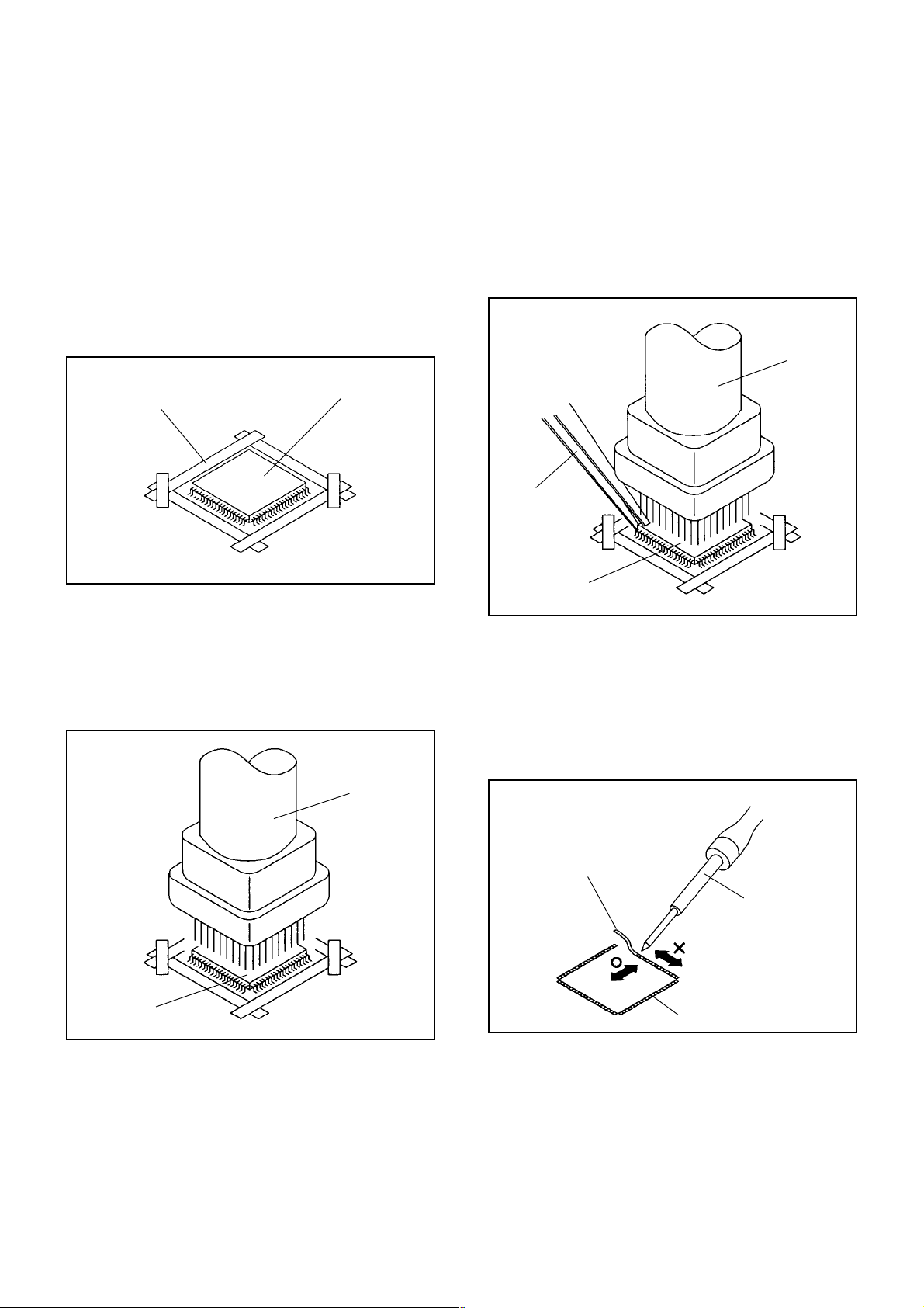
REMOVAL
Put Masking Tape (cotton tape) around the Flat Package
1.
IC to protect other parts from any damage.
(Refer to Fig. 2-1.)
NOTE
Masking is carried out on all the parts located within
10 mm distance from IC leads.
When IC starts moving back and forth easily after
3.
desoldering completely, pickup the corner of the IC using
tweezers and remove the IC by moving with the IC
desoldering machine. (Refer to Fig. 2-3.)
NOTE
Some ICs on the PCB are affixed with glue, so be
careful not to break or damage the foil of each IC
leads or solder lands under the IC when removing it.
Blower type IC
desoldering
machine
Masking Tape
(Cotton Tape)
Heat the IC leads using a blower type IC desoldering
2.
IC
machine. (Refer to Fig. 2-2.)
NOTE
Do not rotate or move the IC back and forth , until IC
can move back and forth easily after desoldering the
leads completely.
Blower type IC
desoldering machine
Fig. 2-1
Tweezers
IC
Peel off the Masking Tape.4.
Absorb the solder left on the pattern using the Braided
5.
Shield Wire. (Refer to Fig. 2-4.)
NOTE
Do not move the Braided Shield Wire in the vertical
direction towards the IC pattern.
Fig. 2-3
Braided Shield Wire
Soldering Iron
IC
Fig. 2-2
IC pattern
Fig. 2-4
B2-1
Page 14

DISASSEMBLY INSTRUCTIONS
INSTALLATION
Take care of the polarity of new IC and then install the
1.
new IC fitting on the printed circuit pattern. Then solder
each lead on the diagonal positions of IC temporarily.
(Refer to Fig. 2-5.)
Soldering Iron
Solder temporarily
Supply the solder from the upper position of IC leads
2.
Solder temporarily
sliding to the lower position of the IC leads.
(Refer to Fig. 2-6.)
Fig. 2-5
When bridge-soldering between terminals and/or the
4.
soldering amount are not enough, resolder using a Thintip Soldering Iron. (Refer to Fig. 2-8.)
Thin-tip Soldering Iron
IC
Fig. 2-8
Finally, confirm the soldering status on four sides of the
5.
IC using a magnifying glass.
Confirm that no abnormality is found on the soldering
position and installation position of the parts around the
IC. If some abnormality is found, correct by resoldering.
NOTE
When the IC leads are bent during soldering and/or
repairing, do not repair the bending of leads. If the
bending of leads are repaired, the pattern may be
damaged. So, always be sure to replace the IC in this
case.
Soldering IronSolder
IC
Absorb the solder left on the lead using the Braided
3.
Supply soldering
from upper position
to lower position
Shield Wire. (Refer to Fig. 2-7.)
NOTE
Do not absorb the solder to excess.
Soldering Iron
IC
Braided Shield Wire
Fig. 2-6
Fig. 2-7
B2-2
Page 15

SERVICE MODE LIST
This unit is provided with the following SERVICE MODES so you can repair, examine and adjust easily.
To enter to the SERVICE MODE function, press and hold both buttons simultaneously on the main unit and on the remote
control for more than the standard time in the appropriate condition. (See below chart.)
Set
Condition
POWER ON
POWER ON
POWER ON
POWER ON
Set Key Operations
VOL. DOWN
(Minimum)
VOL. DOWN
(Minimum)
VOL. DOWN
(Minimum)
VOL. DOWN
(Minimum)
Remocon
Key
1 2 sec.
2
6
9 2 sec.
Standard
Time
2 sec.
2 sec.
Initialization of factory TV data.
NOTE:
Check of the SUM DATA, POWER ON total hours, MICON
VERSION and DIGITAL TV MICON FIRMWARE on the screen.
Refer to the "WHEN REPLACING EEPROM (MEMORY) IC".
POWER ON total hours are displayed on the screen.
Can be checked of the INITIAL DATA of MEMORY IC.
Refer to the "WHEN REPLACING EEPROM (MEMORY) IC".
Display of the Adjustment MENU on the screen.
Refer to the "ELECTRICAL ADJUSTMENT" (On-Screen Display
Adjustment).
If you set factory initialization, the memories are reset such
as the channel setting, and the POWER ON total hours.
C-1
Page 16

WHEN REPLACING EEPROM (MEMORY) IC
CONFIRMATION OF CHECK SUM, MICON VERSION AND DIGITAL TV MICON FIRMWARE
AND POWER ON TOTAL HOURS
Initial total of MEMORY IC, MICON VERSION, Digital TV MICON Firmware and POWER ON TOTAL HOURS can be
checked on the screen. Total hours are displayed in 16 system of notation.
NOTE:
If you set a factory initialization, the total hours is reset to "0".
Please refer to "CONFIRMATION OF INITIAL DATA" when SUM DATA is not corresponding.
Turn on the POWER, and set to the TV mode.
1.
Set the VOLUME to minimum.
2.
Press both VOL. DOWN button on the set and Channel button (2) on the remote control for more than 2 seconds.
3.
After the confirmation of MICON VERSION and Digital TV MICON Firmware, turn off the power.
4.
ADDRESS and DATA should appear as FIG 1.
NOTE: The each item value might be
different according to each set.
Version
Initial setting data check sum.
AD CONVERTER data check sum.
Main Micon Fimware Version
Sub Micon Fimware Version
Hardware version
Software version
OK
INIT: 2ED0
VCT-P: 3451
ANALOG M: DB060-70328A
ANALOG S: DB050-70330A
A.0
CB00C74021
LCD ON: 0000
FIG. 1
Firmware Version
END
POWER ON total hours.
= (16 x 16 x 16 x thousands digit value)
+ (16 x 16 x hundreds digit value)
+ (16 x tens digit value)
+ (ones digit value)
CONFIRMATION OF INITIAL DATA
If a service repair is undertaken where it has been required to change the MEMORY IC, the following steps should be taken to
ensure correct data settings while making reference to INITIAL SETTING TABLE (Attached "INITIAL DATA").
Turn on the POWER, and set to the TV mode.
1.
Set the VOLUME to minimum.
2.
Press both VOL. DOWN button on the set and Channel button (6) on the remote control for more than 2 seconds.
3.
ADDRESS and DATA should appear as FIG 2.
ADDRESS DATA
INIT 0000 00
LDC ON 0000
ANALOG M: DB060-70328
ANALOG S: DB050-70330
FIG. 2
ADDRESS is now selected and should "blink". Using the UP/DOWN buton on the remote, step through the ADDRESS
4.
until required ADDRESS to be changed is reached.
Press RIGHT/LEFT button to select DATA. When DATA is selected, it will "blink".
5.
Again, step through the DATA using UP/DOWN button until required DATA value has been selected.
6.
Pressing RIGHT/LEFT button will take you back to ADDRESS for further selection if necessary.
7.
Repeat steps 4 to 6 until all data has been checked.
8.
When satisfied correct DATA has been entered, turn POWER off (return to STANDBY MODE) to finish DATA input.
9.
After the data input, set to the initializing of shipping.
Turn POWER on.
10.
Press both VOL. DOWN button on the set and Channel button (1) on the remote control for more than 2 seconds.
11.
After the finishing of the initializing of shipping, the unit will turn off automatically.
12.
The unit will now have the correct DATA for the new MEMORY IC.
C-2
Page 17

SERVICING FIXTURES AND TOOLS
JG201 Serial Communication
Change JIG
Ref. No.
JG176
JG201
Part No.
APJG176133JG176
APJG212003JG212
APJG201000
JG203 MICON PROGRAM JIG KIT
25-4
Parts Name
EU LCD MICON VER
UP ROM DISC
DTV ROM DISC
EEP ROM DISC
Serial Communication
Change JIG
JG176
JG212
JG204
Up-Date of the VCTP DATA.
Up-Date of the Digital Soft Firmware.APJG176130
Up-Date of the EEPROM DATA.
Connect the set to personal computer.
EU LCD MICON VER UP
ROM DISC
DTV ROM DISC
EEPROM DISC
MICON UPDATE TOOL DISC
Remarks
JG203
JG204
APJG203000
APJG204000
MICON PROGRAM
JIG KIT 25-4
MICON UPDATE TOOL
DISC
INSTALL FOR WRITING TOOLS
1.2.Set the MICON UPDATE TOOL DISC (JG204) to PC.
Install the LPT driver.
NOTE :
It is necessary to install according to the PC.
Windows 95/98 : Setup_LptDrv_v0104_9x.exe
Windows 2000/XP : Setup_LptDrvDev_v020201_XP_2000.exe
Windows NT : Setup_LptDrv_v0104_NT.exe
Connect the set to personal computer.
There is WRITING TOOLS in Disc.
Re-boot the PC.
3.
Install the “Setup_Visual_I2C_v3-2-3b8h.exe”, “Setup_VI2C_for_VCT_Pro_v0101.exe” and “Winupload 4.4.3.exe”.
4.
C-3
Page 18

RE-WRITE FOR DIGITAL SOFT FIRMWARE
Before UPDATE the Digital Soft Firmware, it is necessary to install the WRITING TOOLS into the PC.
For the installation of WRITING TOOL, refer to the "INSTALL FOR WRITING TOOLS".
Unplug the AC cord, and remove the back cabinet.
1.
Using the Serial Communication Change JIG (JG201) and RS232 Cable, connect the PC terminal and UART
2.
Connector(CP2402) on the MAIN PCB.
UART Connector(CP2402)
MAIN PCB
Connect it in order of MAIN PCB Serial Communication Change JIG(JG201) RS232 Cable PC.
Serial Communication Change JIG(JG201)
TO MAIN PCB
Insert the AC cord, turn on the power.
3.
RS232 Cable
TO PC
Press both VOLUME DOWN button on the set and Channel button (2) on the remote control for 2 seconds.
4.
Confirm that displayed software version.
Set the Standby mode.
5.
Set the DTV ROM DISC(JG176) to PC.
6.
C-4
Page 19

RE-WRITE FOR DIGITAL SOFT FIRMWARE
7. Start the "Winupload"(Writing tool).
8. Select the "Port Setting" from Process menu, then please set it as follows.
NOTE: This step is not necessary from next time.
C-5
Page 20

RE-WRITE FOR DIGITAL SOFT FIRMWARE
Select the "Connect" from File menu.
9.
Select the "Upload" from Process menu, and select the Software(CB00C74021.urt) in DTV ROM DISC(JG176).
10.
Unplug the AC cord on the set, then plug it in again.
11.
Turn on the power.
12.
The following window will appear, Up-date for Software will start.
"Uploading inprogress" bar will begin to move.
C-6
Page 21

RE-WRITE FOR DIGITAL SOFT FIRMWARE
13.
When the "Uploading inprogress" bar reaches a right edge, the Writing for Digital Soft Firmware will start.
During the writing for Digital Soft Firmware, writing message will appear on the screen.
Finish the writing for Digital Soft Firmware, writing message will disappear.
14.
Unplug the AC cord, and remove the Serial Communication Change JIG(JG201).
15.
Insert the AC cord again.
After the write, set to the initializing of shipping.
16.
Turn on the power.
17.
Press both VOLUME DOWN button on the set and Channel button (1) on the remote control for 2 seconds.
The set will turn into the standby mode.
Check for the Firmware Version
18.
Turn on the power.
19.
Press both VOLUME DOWN button on the set and Channel button (2) on the remote control for 2 seconds.
When the changed version displays, the Re-write will be completed.
20.
Select the "Disconnect" from File menu.
C-7
Page 22

UPDATE FOR VCTP SOFTWARE
Before Update the VCTP Software, it is necessary to install the WRITING TOOLS into the PC.
For the installation of WRITING TOOLS, refer to the "INSTALL FOR WRITING TOOLS".
1.
Unplug the AC cord, and remove the back cabinet.
2.
Short circuit the 1 pin and 2 pin of CP802 on the Main PCB.
3.
Insert the AC cord.
4.
Remove the short circuit 1 pin and 2 pin of CP802 on the Main PCB.
5.
Set the EU LCD MICON VER UP ROM DISC (JG176) to PC.
6.
Start the "VCTP" (Writing Tools).
7.
Select the "LPT Preferences" from File/Preferences menu, then input "5" to the value of "Delay", and press "OK".
NOTE: This step is not necessary from next time.
8.
Using the MICON PROGRAM JIG KIT 25-4 (JG203), connect the PC Terminal (LPT Port) and 1~4 pin of
CP802 on the Main PCB (JG203(Red line) =1 pin of CP802).
CP802
Main PCB
C-8
Page 23

UPDATE FOR VCTP SOFTWARE
Press the “TVT”.
9.
Remove the check of “Bootloader Version”, and check it again.
10.
NOTE :
When the number of the side of the check box becomes 40, you can proceed to next step.
If the number doesn’t become 40, check the connection and try again from step 1.
C-9
Page 24

UPDATE FOR VCTP SOFTWARE
11.
Press the “Erase Flash”.
Then, press the “C:\TV\MINTS8\Output\VCTP\Obj\Mints.bin” twice.
Press the , and select the writing Firmware.
12.
...
C-10
Page 25

UPDATE FOR VCTP SOFTWARE
Select the “Address", then input the ”0x7ffff", and press the “OK”.
13.
Press the “Load Bin -> Flash”.
14.
The following window will appear, then writing will start. After the finishing of the writing, window will close.
Finish the writing, unplug the AC cord, and remove the MICON PROGRAM JIG KIT 25-4 (JG203).
15.
Insert the AC cord again, turn on the power.
16.
Press both VOL. DOWN button on the set and Channel button (2) on the remote control for 2 seconds.
17.
Confirm that displayed version agreement with writing.
18.
C-11
Page 26

UPDATE FOR EEPROM DATA
Before Update the EEPROM data, it is necessary to install the WRITING TOOLS into the PC.
For the installation of WRITING TOOLS, refer to the "INSTALL FOR WRITING TOOLS".
Set to the standby mode, and remove the back cabinet.
1.
Using the MICON PROGRAM JIG KIT 25-4 (JG203), connect the PC Terminal and Pin 1-4 of CP802 on the
2.
Main PCB (JG203(Red line) =1 pin of CP802).
CP802
Main PCB
Set the EEP ROM DISC (JG212) to PC.
3.
Start the "VCTP" (Writing Tools).
4.
Press the "NVM".
5.
C-12
Page 27

UPDATE FOR EEPROM DATA
Press the "Change", and select the writing EEPROM data file (TEXT file).
6.
Press the "Update NVM from File".
7.
The following window will appear, writing will start. After the finishing of the writing, the window will close.8.
Finish the writing, unplug the AC cord, and remove the MICON PROGRAM JIG KIT 25-4 (JG203).
9.
Insert the AC cord again, turn on the power.
10.
Press both VOL. DOWN button on the set and Channel button (2) on the remote control for 2 seconds.
11.
Confirm that displayed version agreement with writing.
12.
C-13
Page 28

ELECTRICAL ADJUSTMENTS
1. ADJUSTMENT PROCEDURE
Read and perform these adjustments when repairing the
circuits or replacing electrical parts or PCB assemblies.
CAUTION
Use an isolation transformer when performing any
•
service on this chassis.
When removing a PCB or related component, after
•
unfastening or changing a wire, be sure to put the wire
back in its original position.
When you exchange IC and Transistor with a heat sink,
•
apply silicon grease (YG6260M) on the contact section of
the heat sink. Before applying new silicon grease,
remove all the old silicon grease. (Old grease may cause
damages to the IC and Transistor).
Prepare the following measurement tools for electrical
adjustments.
1. Pattern Generator
On-Screen Display Adjustment
1.2.Set the VOLUME to minimum.
Press the VOL. DOWN button on the set and the
channel button (9) on the remote control for more than
2 seconds to display adjustment mode on the screen as
shown in Fig. 1-1.
PAL
Function
3.
Use the UP/DOWN button or Channel button (0-9) on
01 OSD H POSI 28
the remote control to select the options shown in
Fig. 1-2.
4.
Press the MENU button on the remote control to end the
adjustments.
5.
To display the adjustment screen for TUNER, EXT1,
EXT2, EXT3, Component, HDMI1, HDMI2 and PC
mode, press the button on the remote control.
Press the VOL.DOWN button on the set and the channel
(9) on the remote control for more than 2 seconds.
TUNER
Full
Step No.
Fig. 1-1
FUNCTION
NO.
H POSI OSD
01
V POSI OSD
02
R DRIVE(M)
03
R CUT OFF(M)
04
G DRIVE(M)
05
G CUT OFF(M)
06
B DRIVE(M)
07
B CUT OFF(M)
08
R DRIVE(H)
09
R CUT OFF(H)
10
G DRIVE(H)
11
G CUT OFF(H)
12
B DRIVE(H)
13
B CUT OFF(H)
14
R DRIVE(L)
15
R CUT OFF(L)
16
G DRIVE(L)
17
G CUT OFF(L)
18
B DRIVE(L)
19
B CUT OFF(L)
20
H POSI
21
H POSI MAX
22
FUNCTION
NO.
H POSI MIN
23
V POSI
24
V POSI MAX
25
V POSI MIN
26
BAKLIGHT CENT
27
BAKLIGHT MAX
28
BAKLIGHT MIN
29
BRIGHT CENTER
30
BRIGHT MAX
31
BRIGHT MIN
32
TINT CENTER
33
CONTRAST CENTER
34
CONTRAST MAX
35
CONTRAST MIN
36
CONTRAST 50
37
COLOR CENTER
38
COLOR MAX
39
COLOR MIN
40
TEXT H POSI
41
TEXT V POSI
42
Fig. 1-2
2. BASIC ADJUSTMENTS
2-1: WHITE BALANCE
1.
Place the set in Aging Test for more than 15 minutes.
2.
Receive the gray scale pattern from the Pattern
Generator.
3.
Press the button on the remote control to set to the
AV mode.
4.
Using the remote control, set the brightness and contrast
to normal position.
5.
Activate the adjustment mode display of Fig. 1-1 and
press the channel button (03) on the remote control to
select "R DRIVE(M)".
6.
Press the UP/DOWN button on the remote control to
select the "R DRIVE(M)", "R CUT OFF(M)",
"G DRIVE(M)", "G CUT OFF(M)", "B DRIVE(M)", "B CUT
OFF(M)", "R DRIVE(H)", "R CUT OFF(H)",
"G DRIVE(H)", "G CUT OFF(H)", "B DRIVE(H)", "B CUT
OFF(H)", "R DRIVE(L)", "R CUT OFF(L)", "G DRIVE(L)",
"G CUT OFF(L)", "B DRIVE(L)" or "B CUT OFF(L)".
7.
Adjust the LEFT/RIGTH button on the remote control to
whiten the R DRIVE(M), R CUT OFF(M),
G DRIVE(M), G CUT OFF(M), B DRIVE(M),
B CUT OFF(M), R DRIVE(H), R CUT OFF(H),
G DRIVE(H), G CUT OFF(H), B DRIVE(H),
B CUT OFF(H), R DRIVE(L), R CUT OFF(L),
G DRIVE(L), G CUT OFF(L), B DRIVE(L) or
B CUT OFF(L) at each step tone sections equally.
8.
Perform the above adjustments 6 and 7 until the white
achieved.
D-1
Page 29

ELECTRICAL ADJUSTMENTS
2-2: CONTRAST
1.
Place the set in Aging Test for more than 15 minutes.
2.
Receive the color bar pattern. (RF Input)
3.
Using the remote control, set the brightness and contrast
to normal position.
4.
Press the LEFT/RIGTH button on the remote control until
the contrast step No. becomes "43"
5.
Check if the picture is normal.
6.
Receive the color bar pattern. (VIDEO1 Input)
7.
Using the remote control, set the brightness and contrast
to normal position.
8.
Press the button on the remote control to set to the
EXT1 mode.
9.
Press the LEFT/RIGTH button on the remote control until
the contrast step No. becomes "43".
10.
Check if the picture is normal.
11.
Receive the color bar pattern. (VIDEO2 Input)
12.
Press the button on the remote control to set to the
EXT2 mode. Then perform the above adjustments
3~5.
13.
Receive the color bar pattern. (VIDEO3 Input)
14.
Press the button on the remote control to set to the
EXT3 mode. Then perform the above adjustments
3~5.
15.
Receive the color bar pattern. (AV RGB Input)
16.
Press the button on the remote control to set to the
Component mode. Then perform the above adjustments
3~5.
17.
Receive the color bar pattern. (S-VIDEO Input)
18.
Press the button on the remote control to set to the
HDMI mode. Then perform the above adjustments 3~5.
D-2
Page 30

ELECTRICAL ADJUSTMENTS
2-3: Confirmation of Fixed Value (Step No.)
Please check if the fixed values of each of the adjustment item is set correctly referring below. (TUNER/EXT/COMPONENT/HDMI/PC/DTV)
TUNER
NO. FUNCTION Step No. Step No. Step No. Step No. Step No. Step No. Step No. Step No. Step No. Step No. Step No. Step No. Step No. Step No. Step No. Step No. Step No. Step No. Step No. Step No. Step No. Step No. Step No. Step No. Step No. Step No. Step No.
1 OSD H POSI 26 26 26 26 26 26 26 26 26 26 26 26 26 26 26 26 26 26 26 26 26 26 26 26 26 26 26
2 OSD V POSI 7777777777777777777772677 7 77
3 R DRIVE (N) 850 850 850 850 850 850 850 850 850 850 850 850 850 850 850 850 850 850 850 850 850 850 850 850 850 850 850
4 R CUT OFF(N) 000000000000000000000-- - - - 0
5 G DRIVE(N) ADJ ADJ ADJ ADJ ADJ ADJ ADJ ADJ ADJ ADJ ADJ ADJ ADJ ADJ ADJ ADJ ADJ ADJ ADJ ADJ ADJ ADJ ADJ ADJ ADJ ADJ ADJ
6 G CUT OFF (N) ADJ ADJ ADJ ADJ ADJ ADJ ADJ ADJ ADJ ADJ ADJ ADJ ADJ ADJ ADJ ADJ ADJ ADJ ADJ ADJ ADJ - - - - - ADJ
7 B DRIVE (N) ADJ ADJ ADJ ADJ ADJ ADJ ADJ ADJ ADJ ADJ ADJ ADJ ADJ ADJ ADJ ADJ ADJ ADJ ADJ ADJ ADJ ADJ ADJ ADJ ADJ ADJ ADJ
8 B CUT OFF (N) ADJ ADJ ADJ ADJ ADJ ADJ ADJ ADJ ADJ ADJ ADJ ADJ ADJ ADJ ADJ ADJ ADJ ADJ ADJ ADJ ADJ - - - - - ADJ
9 R.DRIVE (C) 850 850 850 850 850 850 850 850 850 850 850 850 850 850 850 850 850 850 850 850 850 - - - - - 850
10 R CUT OFF (C) 000000000000000000000- - - - - 0
11 G DRIVE (C) ADJ ADJ ADJ ADJ ADJ ADJ ADJ ADJ ADJ ADJ ADJ ADJ ADJ ADJ ADJ ADJ ADJ ADJ ADJ ADJ ADJ - - - - - ADJ
12 G CUT OFF (C) ADJ ADJ ADJ ADJ ADJ ADJ ADJ ADJ ADJ ADJ ADJ ADJ ADJ ADJ ADJ ADJ ADJ ADJ ADJ ADJ ADJ - - - - - ADJ
13 B DRIVE (C) ADJ ADJ ADJ ADJ ADJ ADJ ADJ ADJ ADJ ADJ ADJ ADJ ADJ ADJ ADJ ADJ ADJ ADJ ADJ ADJ ADJ - - - - - ADJ
14 B CUT OFF (C) ADJ ADJ ADJ ADJ ADJ ADJ ADJ ADJ ADJ ADJ ADJ ADJ ADJ ADJ ADJ ADJ ADJ ADJ ADJ ADJ ADJ - - - - - ADJ
15 R.DRIVE (W) 850 850 850 850 850 850 850 850 850 850 850 850 850 850 850 850 850 850 850 850 850 - - - - - 850
16 R CUT OFF (W) 000000000000000000000- - - - - 0
17 G DRIVE (W) ADJ ADJ ADJ ADJ ADJ ADJ ADJ ADJ ADJ ADJ ADJ ADJ ADJ ADJ ADJ ADJ ADJ ADJ ADJ ADJ ADJ - - - - - ADJ
18 G CUT OFF (W) ADJ ADJ ADJ ADJ ADJ ADJ ADJ ADJ ADJ ADJ ADJ ADJ ADJ ADJ ADJ ADJ ADJ ADJ ADJ ADJ ADJ - - - - - ADJ
19 B DRIVE (W) ADJ ADJ ADJ ADJ ADJ ADJ ADJ ADJ ADJ ADJ ADJ ADJ ADJ ADJ ADJ ADJ ADJ ADJ ADJ ADJ ADJ - - - - - ADJ
20 B CUT OFF (W) ADJ ADJ ADJ ADJ ADJ ADJ ADJ ADJ ADJ ADJ ADJ ADJ ADJ ADJ ADJ ADJ ADJ ADJ ADJ ADJ ADJ - - - - - ADJ
21 H POSI 50 Hz (4:3) 642 642 642 642 - - - - 608 284 - - - - - - - 76 5 - - - - - - - 578
H POSI 50 Hz (4:3) OTHER 625 625 625 642 - - - - 608 284 307 256 - - - - - 76 5 138 38 - - - - - 578
H POSI 60 Hz (4:3) 584 584 584 582 560 266 - - - - - - 52 5 5 - - - - - - 129 191 279 258 344 554
H POSI CENTER (PC) 584 584 584 582 560 266 - - - - - - 52 5 5 - - - - - - 129 191 279 258 344 554
H POSI 60 Hz (4:3) OTHER 586 586 586 582 560 266 306 256 - - - - 52 5 5 92 33 - - - - 129 191 279 - - 545
22 H POSI MAX (PC) - - - - - - - - - - - - - - - - - - - - - 229 291 379 358 444 23 H POSI MIN (PC) - - - - - - - - - - - - - - - - - - - - - 29 91 179 158 244 24 V POSI 50Hz FULL SCREEN/Cinima OTHER 25 25 25 23 - - - - 25 50 22 19 - - - - - 13 37 23 19 - - - - - 25
V POSI 50Hz FULL SCREEN - - - - - - - - - - - - - - - - - - - - - - - - - - 0
V POSI 50Hz Cinema - - - - - - - - - - - - - - - - - - - - - - - - - - 0
V POSI 60Hz FULL SCREEN/Cinima OTHER 19 19 19 17 19 41 21 18 - - - - 8 27 27 21 18 - - - - 26 26 26 23 23 -
V POSI CENTER (PC) 19 19 19 17 19 41 21 18 - - - - 8 27 27 21 18 - - - - 26 26 26 23 23 -
V POSI 60Hz FULL SCREEN - - - - - - - - - - - - - - - - - - - - - 0 - - - - -
V POSI 60Hz Cinema - - - - - - - - - - - - - - - - - - - - - 0 - - - - 25 V POSI MAX - - - - - - - - - - - - - - - - - - - - - 51 51 51 51 51 26 V POSI MIN - - - - - - - - - - - - - - - - - - - - - 1 1 1 1 1 27 BAKLIGHT CENTER 128 128 128 128 128 128 128 128 128 128 128 128 128 128 128 128 128 128 128 128 128 128 128 128 128 128 128
28 BAKLIGHT MAX 255 255 255 255 255 255 255 255 255 255 255 255 255 255 255 255 255 255 255 255 255 255 255 255 255 255 255
29 BAKLIGHT MIN 000000000000000000000000 0 0 0
30 BRIGHT CENTER + + + + 16 16 16 16 16 16 16 16 18 18 18 18 18 18 18 18 11 11 20 20 20 20 20
31 BRIGHT MAX + + + + 50 50 50 50 50 50 50 50 50 50 50 50 50 50 50 50 50 50 50 50 50 50 50
32 BRIGHT MIN + + + + -64 -64 -64 -64 -64 -64 -64 -64 -64 -64 -64 -64 -64 -64 -64 -64 -64 -64 -64 -64 -64 -64 -64
33 TINT CENTER + + + + 33333333333333333000 0 0 0
34 CONTRAST CENTER + + + + ADJ ADJ ADJ ADJ ADJ ADJ ADJ ADJ ADJ ADJ ADJ ADJ ADJ ADJ ADJ ADJ ADJ ADJ ADJ ADJ ADJ ADJ ADJ
35 CONTRAST MAX + + + + ADJ ADJ ADJ ADJ ADJ ADJ ADJ ADJ ADJ ADJ ADJ ADJ ADJ ADJ ADJ ADJ ADJ ADJ ADJ ADJ ADJ ADJ ADJ
36 CONTRAST MIN + + + + 18 18 18 18 18 18 18 18 18 18 18 18 18 18 18 18 18 18 18 18 18 18 18
37 CONTRAST 50 + + + + ADJ ADJ ADJ ADJ ADJ ADJ ADJ ADJ ADJ ADJ ADJ ADJ ADJ ADJ ADJ ADJ ADJ ADJ ADJ ADJ ADJ ADJ ADJ
38 COLOR CENTER + + + + 39 39 39 39 39 39 39 39 29 29 29 29 29 29 29 29 34 34 40 40 40 40 40
39 COLOR MAX + + + + 63 63 63 63 63 63 63 63 63 63 63 63 63 63 63 63 63 63 63 63 63 63 63
40 COLOR MIN + + + + 00000000000000000000 0 0 0
41 TEXT H POSI 150 150 150 150 150 150 150 150 150 150 150 150 150 150 150 150 150 150 150 150 150 150 150 150 150 150 150
42 TEXT V POSI 000000000000000000000000 0 0 0
CVBS S(Y/C) RGB 480i 480p 720p 1080i 576i 576p 720p 1080i 480i 480p VGA 720p 1080i 576i 576p 720p 1080i 640x480 800x600 1024x768 1280x720 1360x768
EXT COMPONENT(NTSC) COMPONENT(PAL) HDMI(NTSC) HDMI(PAL)
PC
DTV
NOTE: For the step no. with + mark, please adjust it according to the 2-4.
D-3 D-4
Page 31

ELECTRICAL ADJUSTMENTS
2-4: Confirmation of Fixed Value (Step No.)
Please check if the fixed values of each of the adjustment item is set correctly referring below. (TUNER/EXT)
TUNER
576i 576i 480i
PAL50 PAL60 SECAM PAL50 PAL60 SECAM NTSC3.58 NTSC4.43 PAL50 PAL60 SECAM NTSC3.58 NTSC4.43 PAL50 PAL60 SECAM NTSC3.58 NTSC4.43 PAL50 PAL60 SECAM NTSC3.58 NTSC4.43 PAL50 PAL60 SECAM NTSC3.58 NTSC4.43
NO. FUNCTION Step No. Step No. Step No. Step No. Step No. Step No. Step No. Step No. Step No. Step No. Step No. Step No. Step No. Step No. Step No. Step No. Step No. Step No. Step No. Step No. Step No. Step No. Step No. Step No. Step No. Step No. Step No. Step No.
30 BRIGHT CENTER 18 18 18 16 16 16 16 16 15 15 15 15 15 16 16 16 16 16 16 16 16 16 16 4 4 4 4 4
31 BRIGHT MAX 50 50 50 50 50 50 50 50 50 50 50 50 50 50 50 50 50 50 50 50 50 50 50 50 50 50 50 50
32 BRIGHT MIN -64 -64 -64 -64 -64 -64 -64 -64 -64 -64 -64 -64 -64 -64 -64 -64 -64 -64 -64 -64 -64 -64 -64 -64 -64 -64 -64 -64
33 TINT CENTER 000000 0 0 000 0 0 000 0 0 000 0 0 000 0 0
34 CONTRAST CENTER ADJ ADJ ADJ ADJ ADJ ADJ ADJ ADJ ADJ ADJ ADJ ADJ ADJ ADJ ADJ ADJ ADJ ADJ ADJ ADJ ADJ ADJ ADJ ADJ ADJ ADJ ADJ ADJ
35 CONTRAST MAX ADJ ADJ ADJ ADJ ADJ ADJ ADJ ADJ ADJ ADJ ADJ ADJ ADJ ADJ ADJ ADJ ADJ ADJ ADJ ADJ ADJ ADJ ADJ ADJ ADJ ADJ ADJ ADJ
36 CONTRAST MIN 18 18 18 18 18 18 18 18 18 18 18 18 18 18 18 18 18 18 18 18 18 18 18 18 18 18 18 18
37 CONTRAST 40 ADJ ADJ ADJ ADJ ADJ ADJ ADJ ADJ ADJ ADJ ADJ ADJ ADJ ADJ ADJ ADJ ADJ ADJ ADJ ADJ ADJ ADJ ADJ ADJ ADJ ADJ ADJ ADJ
38 COLOR CENTER 38 38 38 38 38 38 38 34 39 39 38 36 32 38 40 36 36 34 38 40 36 36 34 39 39 39 39 39
39 COLOR MAX 63 63 63 63 63 63 63 63 63 63 63 63 63 63 63 63 63 63 63 63 63 63 63 63 63 63 63 63
40 COLOR MIN 000000 0 0 000 0 0 000 0 0 000 0 0 000 0 0
EXT1(SCART1), EXT2(SCART2) EXT3(RCA) EXT2(SCART2) EXT3(RCA) EXT1(SCART1)
576i 480i 576i 480i
CVBS CVBS S(Y/C)
576i 480i 576i 480i
S(Y/C) RGB
D-5 D-6
Page 32

ELECTRICAL ADJUSTMENTS
TU6002
CP504
3. ELECTRICAL ADJUSTMENT PARTS LOCATION GUIDE (WIRING CONNECTION)
LCD PANEL
CD403
OPERATION PCB
REMOCON PCB
CP2201
CP501
CP2203
OS2201
MAIN PCB
CP2401
CP802
CP101
CP2402
CP5000
CP7201
CD302
SPEAKER
CD3400
FAN
CP1000
CP4304
CP4301
CP3400
CP3801
J4206
CP102
CP3601
J4205
J702
J4200
J4201
J4208
CP4302
AC IN
J501
POWER PCB
D-7
Page 33

POWER DOES NOT TUNER ON
TROUBLESHOOTING GUIDE
Is F501 broken?
No
Is there voltage at pin
10 of IC501 at 18.9V?
Yes
Is there voltage at pin
2 of IC503 at 5V?
Yes
Change MAIN PCB.
Yes
No
No
Change F501.
Check IC501 and peripheral
circuit.
Check IC503 and peripheral
circuit. Or change IC503.
E-1
Page 34

THE PICTURE DOES NOT
APPEAR (1)
Is CD7204 connected?
Yes
TROUBLESHOOTING GUIDE
No
Connected CD7204.
Is there signal at
CP7201 ?
Yes
Check IC803.
Or change SCALER PCB.
No
Change CP7201.
E-2
Page 35

THE PICTURE DOES NOT
APPEAR (2)
TROUBLESHOOTING GUIDE
Is there signal at
IC4205 ?
Yes
Check IC803 and
peripheral circuit.
No
Check IC4205 and
peripheral circuit.
E-3
Page 36

THE PICTURE DOES NOT
APPEAR. (DIGITAL)
TROUBLESHOOTING GUIDE
Does an error
message display it?
NO
Change MAIN PCB.
YES
Change DIGITAL TUNER
MODULE.
E-4
Page 37

THE COLOR DOES NOT
APPEAR
TROUBLESHOOTING GUIDE
Is setting of color
normal?
Yes
Is the color signal
received?
Yes
Check IC803 and peripheral
circuit.
No
Change the setting of color.
No
Receive the color signal.
E-5
Page 38

ON SCREEN DISPLAY DOES
NOT APPEAR
TROUBLSHOOTING GUIDDE
Is there signal at pins
2, 4 of IC101?
Yes
Is there color signal at
pins 83 and
84 of IC803 ?
Yes
Change MAIN PCB.
No
No
Check IC101 and
peripheral circuit.
Check IC803 and peripheral
circuit.
E-6
Page 39

THE SCREEN HAS A VERTICAL
LINE OR A HORIZONTAL LINE.
TROUBLESHOOTING GUIDE
Is there a normal
waveform at pins 184,
187 and 190 of IC803?
Yes
Change IC803.
No
Change V2301.
E-7
Page 40

TU6002 TUNER
SW_SCART_G_OUT
SC2_A_OUT_R
SC2_A_OUT_L
A_R_OUT
V_OUT
AUDIO_OUT_JACK_R
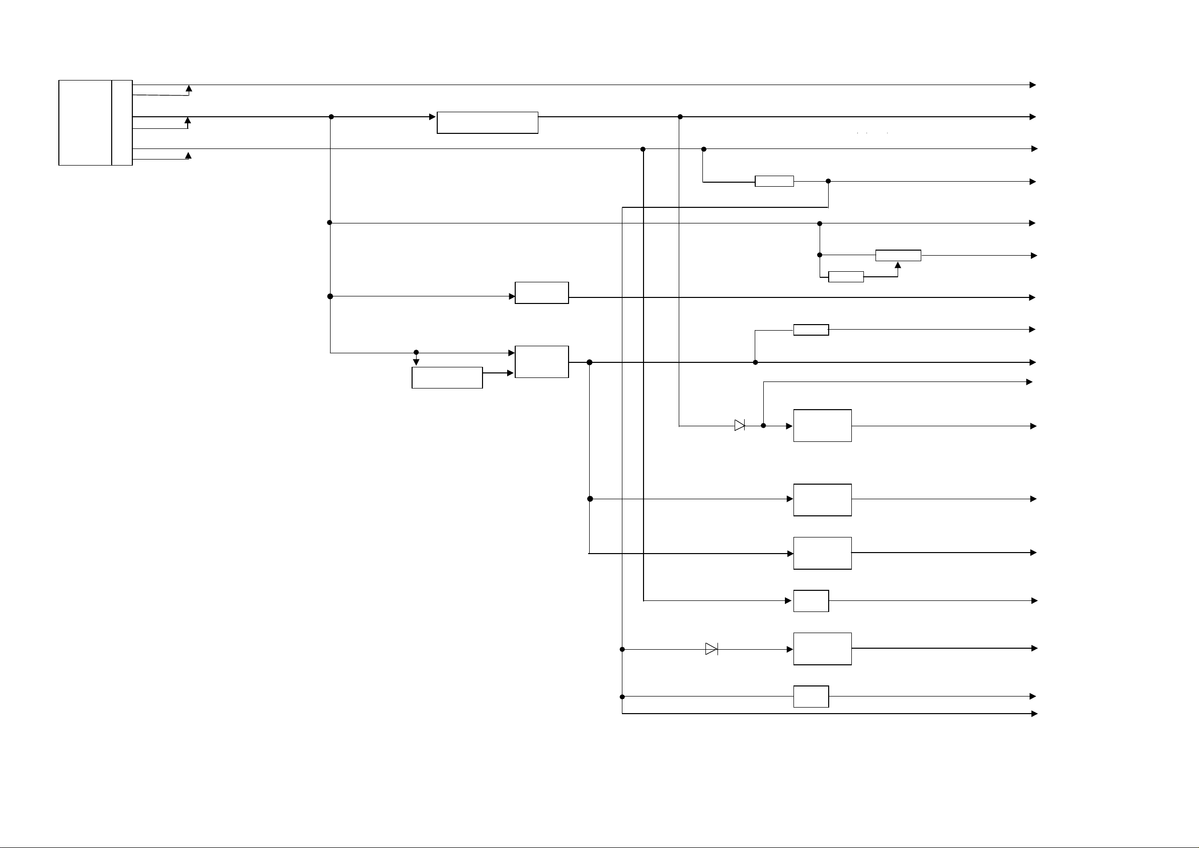
TUNER/SCART1/SCART2/RCA AUDIO OUT BLOCK DIAGRAM
AGC 4 RF_AGC
SCL 9 IC6001 BUS_SW
SDA 10 15
CVBS 15
IF AGC 18
DIF1 19 DIF1
DIF2 20 DIF2
SCL F_SCL
SDA F_SDA
14
D_TUNER_SCL
D_TUNER_SDA
1 F_SCL
13 F_SDA
2 D_TUNER_SCL
12 D_TUNER_SDA
SCALER/
SUB
IF_AGC
IC4201 TUNER_OUT_CVBS_SW
6 TU_TUNER_CVBS_IN D_TUNER_CVBS_IN 4 D_TUNER_CVBS
2 OUT
J4206 SW_CVBS_(TU/D_TU)
R_OUT
L_OUT
1 SC1_A_OUT_R
3 SC1_A_OUT_L
SCART1_Y_IN
L_IN
R_IN
2
6
IC4204 SCART1/2_RGB_SW
SCART 1
21-B_IN
21-G_IN
21-R_IN
(21-C_IN)
21-Y_IN
7 8 SCART1_B_IN SW_SCART_R/C_OUT 3 SW_SCART_R/C
11 11 SCART1_G_IN
5 SW_SCART_G
15 16 SCART1_R_IN SW_SCART_B_OUT 6 SW_SCART_B
16 1 SCART2_R/C_IN
9 SCART2_B_IN
FOR_VCR
8 14 SCART2_G_IN
SCART1_SW
TUNER OUT 19
VIDEO IN
20 IC4203 SCART1/2_AUDIO_Lch_SW
4 SC2_A_IN_L A_L_OUT 2 SW_A_L
R_OUT
L_OUT
22
24
(SCALER IC803 21pin) 6 SC1_A_IN_L
(SCALER IC803 22pin)
SCALER/SUB
MICON
SOUND AMP/
HEADPHONEJACK/
COMPONENT
SCART2
L_IN
R_IN
21-B_IN
21-G_IN
21-R_IN
(21-C_IN)
21-Y_IN(FB)
FOR_VCR
MONITOR OUT
VIDEO IN
23 IC4202 SCART1/2_AUDIO_Rch_SW
27 4 SC2_A_IN_R
28
32 IC4206 SCART1/2_VIDEO_SW
36 4 SCART2_V_IN
37 SCART2_FB(Y_IN)
29 SCART2_SW
40 SC2_CVBS_OUT
41
J702 AV_AUDIO_IN/S-TERMINAL_JACK
S_Y_IN 7
S_C_IN 8
V_IN 2
L_IN 3
R_IN 11
J4202 AUDIO _OUT_JACK
L_OUT 3
R_OUT 2
6 SC1_A_IN_R
6 SCART1_V_IN
2 SW_A_R
2 SW_SCART_CVBS/Y
S_JACK_C/ S_JACK_Y
CVBS_IN
VIDEO_A_L
VIDEO_A_R
AUDIO_OUT_JACK_L
SCALER/
SUB
F-1 F-2
Page 41
CP3801
P.CON+9V
P.CON+5V
Q3814
P.CON+8V
AT+1.8V_1
AT+1.8V_2
POWER/REGULATOR BLOCK DIAGRAM
SOUND+B 1 SOUND+B
SOUND+B 2
IC3801 REG
SW+12V 8
SW+12V 9
AT+5V 14 AT+5V
AT+5V 15
Q3812 SW
SW+12V
DTV+4V
IC304
Q3805/Q3804 SW_TR
P.CON+12V_DTV
Q3200 SW
P.CON+3.3V
Q3202
AT+3.3V
IC3203
IC3205 5V_REG
P.CON+5V VCP
D3804
IC3203 REG
IC3204 REG
Q3806 SW
P.CON+5V_DTV
IC3201 3.3V_REG
HDMI+3.3V
D3202
Q3205 SW
HDMI_5V
HDMI_VNREG+5V
F-3 F-4
Page 42

CP4301
STAND_BY_LED
CP4304
SCALER/SUB MICON BLOCK DIAGRAM
RS232_RXD
RS232_TXD
SOUND AMP/
HEADPHONE
JACK/
COMPONENT
CP3801
LCD+B 18
LCD+B 19
DTV_H
DTV_LPM_CTL_H
LPM_INT
DTV_RESET
DTV_TX/RX
DTV_TX/RX
D_TUNER_AUDIO_L
D_TUNER_AUDIO_R
SW_Y/D_Y
SW_PB/D_PB
SW_PR/D_DR
AUDIO_OUT_JACK_L/R
VIDEO_A_L/R
CP7201 LCD PANEL
LVDS+/-
10 106 91/92 102 88 87 128 SW_A1_R
9 129 SW_A1_L
131 ~ 135 VGA-R/G/B
137 ~ 141 SDA/SCL
179~181
REMOCON
25/26 89
EPG_LED 100
13/14
117
V2301
HDMI/D-SUB
REMOCON_PCB
TUNER/
SCART1/
SCART2/ RCA
AUDIO OUT
S_JACK_Y/C
AW_CVBS(TU/D_TU)
SC1_A_OUT_R
SC2_A_OUT_L
SCART1_Y_IN
SC2_A_OUT_R
SC2_A_OUT_L
SW_SCART_R/C
SW_SCART_G
SW_SCART_B
SW_A_R
SW_A_L
SW_SCART_CVBS/Y
SCART2_FB(Y_IN)
SC2_CVBS_OUT
SCART1_SW
SCART2_SW
RF AGC
HP_IN
184/ 187
191 79 X801
23 78 20.25MHz
24
20 KEY_A/B 159/160
21
178
176
177
48 ~73
11 DEN/DCLK IC801 256K EEPROM
12 DRI0~7/DGI0~7/DBI0~7 84 5 SDA
189 83 6 SCL
183 195 8 38 39 40
1
IC802 SYSTEM RESET DEN/DCLK
IC101 SUB MICON R5F21244SNFP IC105 RESET
8 HDMI I2S
42
43
9
41 X101 16MHz
11 Q101/Q102
25 F.SDA 4
F.SCL 2
23 24
M24256-BWNM6TP
DRI0~7/DGI0~7/DBI0~7
OPERATION_PCB
HDMI/D-SUB
SOUND AMP/
HEADPHONE
JACK/
COMPONENT
F-5 F-6
F.SDA
F.SCL
CP102
DIN-901B
RS232_RXD RS232_TXD
IC102
ISL83220ECVZ-T
9 11
2
3
8
13
Page 43

DEN/DCLK
CP4302 D-SUB_CONNECTOR
VGA_VS
39, 40, 43, 44,
HDMI/D-SUB BLOCK DIAGRAM
SW_A1_R
SW_A_L
IC4302 VGA-R/VGA-G
J4208 AUDIO_MINI_PIN_JACK YUV/DVI_Rch_SW VGA-B
PC/DVI1_A_IN_R SDA/SCL
R H-SYNC
V-SYNC
PC/DVI1_A_IN_L
L DRI0~7/DGI0~7/DBI0~7
HDMI_I2S
IC4303 IC3605 HDMI_I/F SiI9025CTU
J4200 AUDIO_IN_JACK YUV/DVI_Lch_SW 110~144
YUV_A_R
R 2
YUV_A_L Q4303
L 4
VGA-R
R 1 VGA-G Q4304 96
G 2 VGA-B X3602 28.322MHz
B 3 97
SDA 12 SDA DDHS
SCL 15 SCL
SCALER/
SUB MICON
VS 14 IC3601 1.8V_REG
HS 13 VGA_HS 94
HDMI+5V
DDVS
31
32 47, 48, 51, 52
DIGITAL
IC3606 SIGNAL
2K EEPROM
BR24L02F-WE2
15
16
HDMI CONNECTOR
CP3601
POWER/
REGULATOR
F-7 F-8
Page 44

J4200 COMPONENT_JACK
SW_Y/D_Y
D_TUNER_AUDIO_R
D_TUNER_CVBS
SOUND AMP/HEADPHONE JACK/COMPONENT JACK BLOCK DIAGRAM
OUT
Y 9 11
PB 7 Y_IN 16 3
PR 6 PB_IN 5 SW_PB/D_PB
PR_IN 1 6 SW_PR/D_PD
IC4205 D.TUNER/YUV_SW
8
9 DTV_LPM_CTL_H
14 D_TUNER_AUDIO_L
DIGITAL_BLOCK
_
DIAGRAM
DTV_TX/RX
DTV_RESET
LPM_INT
SP_AUDIO_OUT_L
SP_AUDIO_OUT_R
DTV_H
AUDIO_MUTE
A_OUT_L
A_OUT_R
IC1000 SOUND_AMP
CVBS 1 J4205 HEAD_PHONE_JACK (SW)
TVTX
2 SPEAKER
TVRX L CP1000
RESET 4
Y R
D.TUNER YUV
U
V HEAD_PHONE
DTV-H
SCL/SDA
SCALER/ SUB
MICON
TUNER/SCART
1/SCART2/
RCA AUDIO
DIF1
DIF2
IF_AGC
IF_AGC
DIF2
DIF1
D_TUNER_SCL
D_TUNER_SDA
F-9 F-10
Page 45

AUDIO_L+L-
AUDIO_R+R-
C, D, F
AOUTR
AOUTL
CVBS
TVTX
TVRX
POWER CTL
RESET
YUV
12V
5V
3.8V
DTV_H
LPM_INT
SCLT/SDAT
IF+/-
IF_AGC
DDR
256Mbit
IC2403
B
A, B, E
DIGITAL BLOCK DIAGRAM
FLASH
16Mbit
IC240
E
Digital IF+/-
12C
OFDM
STV0362
IC4001
G
Flash ROM
Update
CP2402
MEPGTS
12C
TXR
E
EEPROM64K
M24C4WMN6TP
IC2409
G
Common Interface
(PCMCIA)
CP3001/3002
MPEG
STM5105
IC2401
A. 1.2V
B. 2.5V
C. 1.0V
AUDIO
OPEAMP
TSH73CD
IC6406
REG
IC6401.6402
IC6405.6407
E. 3.3V
F. 3.3V
REG
IC6403
IC6404
F-11 F-12
Page 46

POWER BLOCK DIAGRAM
432
F501
L507
VH
Vcc
FB
T501
J501
432
1
L510
OUT
L506
+
1
1
7
78
5
AC IN
CD501
D506
2
4
3
2 5 6 8
IC501
FA5541AP-A2
1 432
5V REG
IC503 LA5779
IN
TRANSFORMER
1
C507
6
8
D501
FCF10A20
5
9
3
10
13V REG
IC504 LA5779
IN
OUT
1 2
OUT
CTL
1
5
2
11
CP501_1,2,3.4,5.+24V
CP504_14,15. AT+5V
CP504_1,2. SOUND+B
CP504_8,9. SW+12V
12
CP504_11.SYS POWER-H
G
Q501
2SK3538-01MR
D
S
IC506
PS2561AL1-1-V(W)
134
2
REGULATOR
IC502 KIA431A-AT
3
1
12V REG
IC505 BA00BC0WT-V5
CTL
5
OUT
2
IN
1
CP504_18,19. LCD+B
CP504_17. PANEL_POWER_H
F-13 F-14
Page 47
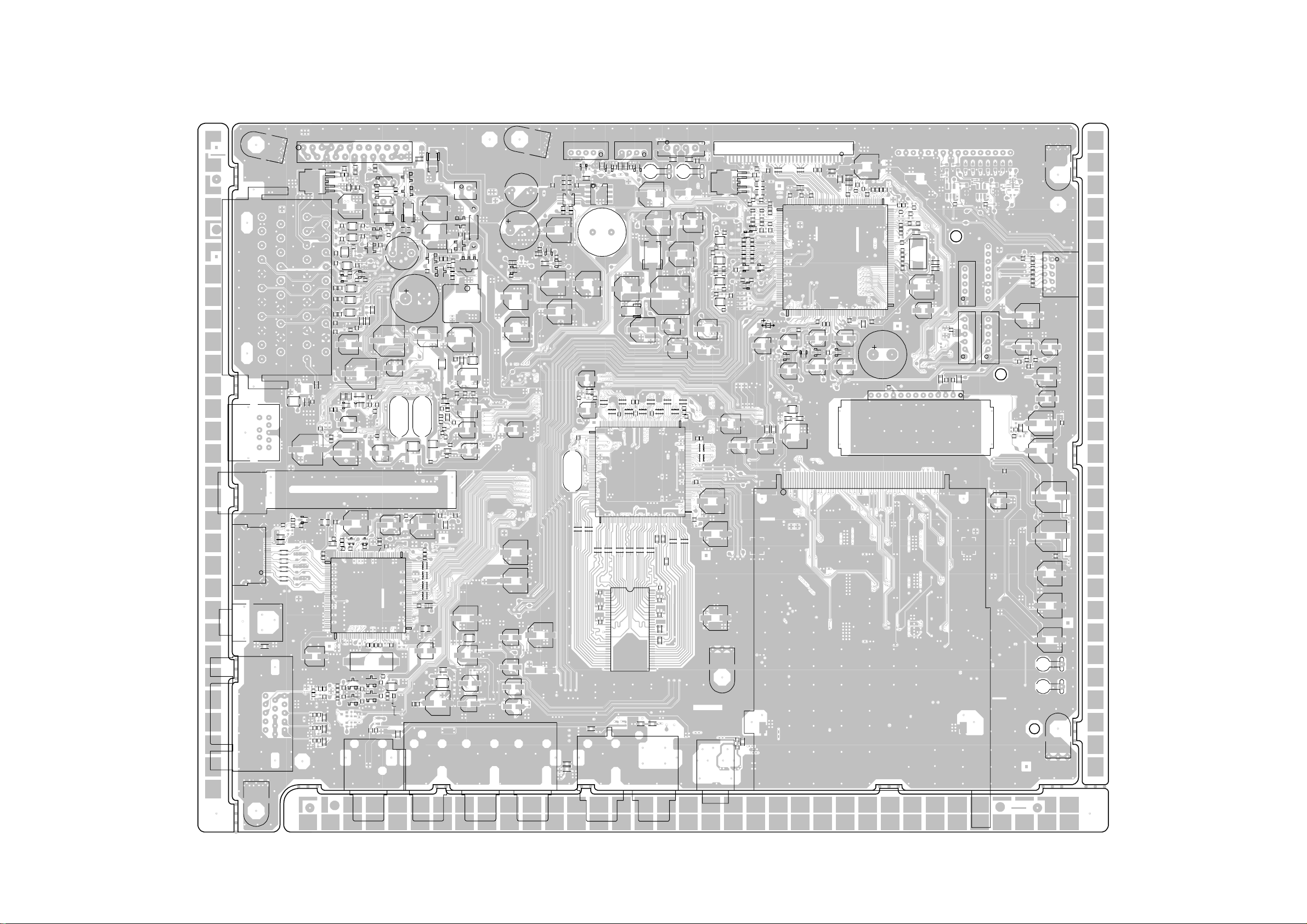
PRINTED CIRCUIT BOARDS
MAIN (TOP SIDE)
J4208
CP102
CP3601
CP4302
W905
SH4300
J4206
R3715
D3601
D3603
L3601
L3603
L3602
L3604
R3716
R3601
NR2409
NR2407
C4250
W872
C4363
C3812
C2436
B1002
NR2410
R2446
NR2411
C2461C2460 C2459
R2450 C2447
B1003
C6406
C4283_1
NR2412
R2447
NR2403
R2448
CP1000
C4227
55
C4277
1
B1001
NR2413
R2434
R2433
C2435
NR2402
B1005
C4383
R2416
W826
C2408
C2410
C4222
C2409
NR2418
R907
C912
R906
C918
NR2419
C2433
C2421
C2448
J4205
C915
C909
L809
L808
L810
L807
SH4306
CP7201
R1011
B1006
SH4304
R2407R2405
R2403
R2408
R2402
R2411
R2404
R2401
C821
R1012
R1001
C1008
C1003
CP2401
C1007C1004
C1009
C1002
W1010
C1011
C1015
W855
C6460
C6468
C5021
B4300
B4308
SH4305
IC803
C801
C805
R835
C802
C807
R832
R837
R895
R894
R893
R808
C870
C875
C872
C876
W809
C863
D826D825
C864
CP5000
R897
R896
C1010
W854
R848
C886
R914
R915
C888
W818
C885
C884
C887
C891
R843
R852
R912 R911
B810
IC1000
HS301
X801
B806
B809
C806
C893
W893
C1024
C1006
105157
C1005
C1023
CP2402
CP101
W702W700
CP802
R1000
R1003
R1006
W853
C5003
R3217
R3215
C3231
IC3203
C3227
R3210
C3229
C3225
R873
R810
R802 W841
R913
R805
D805
C917
D811
R855
C819
R868
C827
R857
C838
R862
C820
R859
C828
R863
C839
D812
C2446
D803
R800
R861
C835
D830
C911
C892_1
C857
C6465
C6464
C4263
W886
C4266
C914
R908
C920
C910
NR802NR801
R828
R3218
R872
C843
R807
R813
R814
C889
R827
B813
C850C845C844
1 53
C855
R824
R823
C861
C858
D823
D824
C862
C859
L6406
B6403
C6403
B6402
B6401
C6442
B801
R826 R825
R4350
C4381
D4209
C6443
C3242
C6436
C3805
L3804
SH4301
R4345
C4377
C4380
CP3801
R3801
W820
R3831
IC3801
C4207
C4215
R4274
C4220
C4233 C4230
C4245
R4272
W852
L101
C106
C103
R109
R108
R113
R119
R112
C6006
R3830
C4202
C4212
L4212
D4211
R4227
R4242
D107
C6003_1
R4218
L4215
W850
C4238
C105
C116
C3815
L4211
L4216
L4205
L4204
L4218
R3832
C3808
C104
R3806
R4251
C3807
C4218
IC105
R3829
R4250
D4210
R4239
R4289
TU6002
R4224R4223
R4273
R4254
R4247
R4203
R3805
Q4210
C108
R114
Q4205
W864
C117
Q3806
Q3812
D3205
R4268
C115
C118
C112
C4217
R4264
R3816R3815
R3841R3840
C4241
L3201
X101
C3241
Q3807
Q3811
D3804
L102
C3201
B3801
R3812
C4239
X1700
D3802
C3240
C3238
Q3803
L1703
W811
C1745
C1709
C1707
C1712
C1708
C1716
C1714
C3801
Q3801
C1746
L1702
B1702
B1701
R3811
C1723
C1721
C1722
R3807
R3803
R3804
C1711
CP3400
Q3804
R3808
R3813
C3802
Q3805
R3814
R3810
Q3802
R3809
L3202
C4242
L1700
C1742
B1700
C1740
C1735
C1734 C1733
C1737
C1710
C1725
C1738
CMF112A
D4217
C6419
C3810
C3806
R3836
C4379
R4349
D4220
C6416
R3835
R3834
IC3804
CP4301
D4305
B4306
C3816
R3838
C3818
C6415
C2465
D2402
R2414 R2413
C2402
R6425
X2401
L3805
NR2414
109
B4313
Q3814
NR2415
D4306
C4364
NR2416
C2438
NR2417
B4312
C6408
CP4304
B4322
D6406
C4372
R2457
C2437
IC2401
D4312
C4216
R2456
NR2408
163
C3694
C3625
C4262
C3693
C3610
R3697
C4256
R3698
R4329
C4356
R4319
C3654
C3637
L4305
109
R3699
R4334
C4355
C6009
137
R4337
W877
R3689
C4352
C6010
C4334
R3669
R3617
R3615
C3616
C4328
B3605
NR3601
NR3602
NR3603
NR3604
C4353
L4306
B4317
R6004
B6001
R6014
C4299
C4293
L4226
C4287
C4289
J4200_1
C4297
C4296
C4290
C4288
C3615
C3659
C4295
W869
W863
NR2401
NR2420
NR2422
W875
NR2404
C2458 C2457 C2456
J702
NR2421
NR2406NR2405
IC2403
W889
D3630
C3722
R4311
R4310
C3611
R4315
R4312
R4309
C3604
C3609
C3606
R4321R4320
R4314
R4316
C3629
B3601
R3711
C4345
R4322
B4305B4304B4303
C4354
R4332
C4357
R4339
C3619
73
C3721
Q3601 Q3605
R3600
R4331
R4336
R3622
Q4304
Q4307
C3618
R3623
R4330
R4333
IC3605
X3602
Q4303
Q4306
J4201
G-1
SH4307
G-2
Page 48

R4356
R4300
R4234
R4360
R4358
R4362
R884
R839
R878
R840
R853
R845
R846
W831
W830
B808
R1027
C5015
C5007
B805
C5009
R886
C871
NR5011
NR5002
NR5009
R831
R916
R834
R833
W814
R5016
C865
C868
C846
C901
C900
L804
C904
C903
C902
L805
C905
B817
C867
C866
C869
W813
R5018
R5012
R5017
R5013
C5008
C5005
NR5010
IC5003
C5016
IC5000
IC5005
Q5000
R1014
R842
R871
R870
R869
C881
R849
R851
R858 R856
B818
R1017
R1015
R5001
R5011
R5010
C5004
R5000
C5017
IC5004
NR5000
NR5005NR5004
IC5002IC5001
R5008
W849W842
C804
R815
R812
IC802
C829
D804 D802
C831
C818
B1004
W857
R1005
Q1000
W858
R4359
D6402
R4355
W861
R6411
R6412
L5000
IC6403
C6463
C6471
B5000
R6452
R6463
C5001
R6453
C5013
C5012
L5001
C5011
C5023
R5004
R6454
C5022
C5010
B5001
C5020
Q5002
C5000
C5019
R5006
R5007
Q5001
R5002
R5005
R5003
W805
W824
C5002
C5018
C5014
R5020
NR5001
NR5007 NR5006
IC801
C808
R5009
PRINTED CIRCUIT BOARDS
MAIN (BOTTOM SIDE)
IC3204
R6438
R850
C6444
W925
C830
C6461
D833
C6405
R867
C860
D814
R6446
R6403
C822
W851
D834
L6401
C6402
B7201
C7201
C3228
C3230
R909
R817
R811
D831
D813
C832
C834
D808
C825
D835
R816
C826
C833
R821
R820
R6431
R6433
IC6406
C6401
R6428
C6447
L6409
W884
C6456
R875
R860
R866
B819
C6452
C3232
R3213
R3219
C3226
R3220
C894
Q4216
C2420
C2449
R2451
C897
W833
B2402
C2462
W829
R4279
B2404
C2445
W881
C2432
B2403
C4384
C4385
C4232
B2401
B2405
D4213
D4304
D4214
R2449
R2455
C4282
C4280
C4274
C2444
R2426
R2419
R4352
W801
C4275
C2443
C2425
C2406
W890
D4303
IC4201
C4240
C2427
Q4218
C4382
IC4206
D4215
IC4203
IC4202
C2442
C2407
D4212
C4224
R2431
R2430
R2432
C2414
C2413
C2429
C2419 C2418 C2417 C2416
R4351
B4214
R3216
C908 C907
L806
C906
C899
L802
C896
C898
R865
L803
C895
C890
L800
C841
R4283
R4282
R819
L2402
R6426
C6440
C6450
R6427
R6432
C6451
R6434
R6441
C6462
R6447
W827
R6401
L2403
R6430R6429
C6449C6448
C6454C6453
L6410
L6408
C6458C6457
W885
W876
W928W927
B811
R822
B812
B807
C836
C817
C813
B802
C814
C809
R864
C824
C800
R876
C810
C853
R5014
D809
C852
B803
C815
C840
B804
C816
C803
R917
R818
C851
D816
C856
C849
C848
C847
C854
D815
NR5003
NR5008
R5015
R5019
IC5006
C5006
R4342
R4293
L4223
C4276
L4221
L4214
R2465
R4353
Q4217
R4341
Q4224
L4233
IC2404
L2401
C2454
R2467
R2466
W856
R2464
C2404 C2403
C2451
C2450
Q4214
R4202 R4201
B4205
B4326
B4324
B4309
Q4309
C4358
L4225
C3813
R4212
B3804
B3805
C4251
IC6402 IC6401
R6404
C6407
R6405
R6400
R6406
D6412
L4208
R6414
IC2409
D6404
C2466
C2428
C4214
C2431
R6420
C4235
R6421
R2424
R2429
C2423
L4227
C2464
D6401
C2455
C2401
IC2402
D6405
C6409
R6402
C2422
D3805
C2430
C2434
C2426
R6413
C2463
C2424
D6403
R2415
Q2401
B2406
L2404
C2415
R4327
C6417
C2439
B4208
Q4305
C6413
C2405
C2412
C2411
R4230
C3817
R3229
Q4310
C3213
C4359
Q3808
R3839R3837
R6423
Q4308
R6424
R6407
R3212
B4307
D6410
R3211
R3214
B4318
D4216
C4265
Q3810
C6418
R6422
R4335
R4290
R6418
D6411
IC3201
W819
C4378
IC6407
C6412
C3211
L4219
R3205
R3821
IC4204
C4294
R4226
B4200
R6409
R3245
L4230
D3202
R6410
Q3211
C3212
R6408
D6413
Q3210
D6408
R6419
R3222
C6414
C3214
Q3201
R4298
R6417
D6409
R3221
W897
D3628
D3629
R4304
R4297
R4348
D4219
C4376
D4218
R4346
C4281
IC6405
C6470
R1708
C1726
C1718
C1713
C1706
Q3200
R3209
R3704R3703
Q4223 Q4222Q4221
R4313
R4307
R4295
R4294
R4221
B4207 B4206
R6460
R3246
R1706
R1712
C1732
C3627
R3702
C4291
R6461
C1719
R3244
W914
W860
C3657
R3701
IC4205
R4292
R3207 R3206
R3208
Q3202
B3201
C3217
C6441
R6462
C3216
D6407
R6415
C1744
C1743
R1710
R1711
R1709
C1736
R1713
R1714
33 17
IC1700
1
49
C1701
R1700
C1704
C1703
C1702
R3228
CMF112A
IC3601
C3635
R4306
R4303
R4296
R4291
W865
R4200
C1705
C1700
D3201
C6469
R1716
C4300
C4339 C4337
D3801
C3207
R6416
R1715
C1729
R1702
W812
Q6005
L4231
R4301
IC3205
C3204
C3206
R3201
C3205
IC3202
R3203
R3204
IC6404
R6458 R6457
C1731
C1730
R1704
R1705
C1728
C1727
C1724
R1701
C1715
R6013
R6018
C4348
IC4303
C4350
C4347
C4336
IC4302
C3203
C1717
W848
C3218
C1720
W878
C3639
C3219
C3640
C3202
C6426
R6456
W879
W909
NR3606NR3605
B3609
B3610
C3638
C3632
B3603
L4229L4228
C3237
R131
IC6001
C3712
C3626
C3710
C3709
C3708
R4302
C4312C4311
C3711
C3239
R6022
Q3206
D3203
L4213
R130
C101
R3224
R4228
C6012
R4241
C102
C3633
R4246R4245
L4217
Q102
C3620
B3613
Q101
R4232
C111
C6013
C3701
Q4209
L4210
R6012
R3223
C3698
R6016
R4261
R107
R127
C3696
C3695
R4236
R4238
Q4204
R6001
Q6001
C3642
B3604
R4267
Q4203
R128
C110
B3608
R3625
C3706C3704
R106
R4229
Q4208
R129
W816
C123
C3716
C3697
R4235
R4237
R4249
R4248
R6017
Q6002
Q3205
B3606
R3626
R6019
R4217
W847
W844
W915
R3627
C3700
R4220
1
14
R3636
Q4207
L4209
R4222
D108
R3635
C3692
L4232
L4224
R4225
C3641
L4202
R4219
Q4201
C3714
L4206
L4207
R4210
C3608
B6002
L4203
R4209
R4244
IC101
C3617
R4344
C4201
C4211
C4206
C4213
C4374
R4287
C4285
R4276
B4203
B4204
R4240
R4243
R4215
D105
R115 R110
R116
40
27
R125
R124
D3605 D3600
Q3602
C3643
C3717
C3718
C3602
C3621
C3605
C3607
C3623
C3624
C3628
C3656
C3630
C3655
C3689
C3688
C3690
C3699
C3691
B3602
C3614
C3613
C3612
D4311 D4310
C4333
IC4301
C3622
C4324
D4205
R120 R118
R6009
R6011
IC3606
D4221
C126
C125
R4318
R4324
R104
C4303
C4390
W821
C124
IC102
B6003
B4301
R4354
R4323
W862
D102 D101
R102
B101
B102
R103
D103
C128
C127
D104
W896
C6007
Q3618
R3688
R3605
R3604
R3607
R3606
Q3603
Q3604
C4325
B4302
R4317
D4302D4301
R4328
R3609
C3631
R3628
R3608
W807
W808W837
D4222
G-3
G-4
Page 49

PRINTED CIRCUIT BOARDS
POWER/REMOCON/OPERATION (INSERTED PARTS)
SOLDER SIDE
CP504
C528
CP2201
REMOCON
W016
W018
W019
W012
W805
C2202
SH504
W017
W810
C524
W013
W014
L511
L504
L505
SH503
CEF302A
R2207
5
C533
C525
OS2201
C532
C522
W021
IC504
W020
W011
CEF300A
D2201
IC503
1
L503
C523
PAL
3
EPG TIMER
STAND BY
POWER
CP501
3
L502
HS503
W010
W008
D501
L509
W009
C526
C527
W007
D526
W005
W006
IC505
HS506
W816
D515
C518
DIP
W004
W003
C519
SH502
T501
R515
C515
R517
D513
R521
D518
IC502
R522
R520
R545
R551
C516
IC506
D510
R512
C512
D507_1
R509
L508
D509
R510
C511
R503
IC501
C510
W806
HS501
R550
L507
B501_1
W001
W002
R536
D512
D502
D508
R505
R506
D514
Q501
R540
R511
SH501
C521
C508
D506
C507
TH501
POWER
C558
L506
D505
R504
D504
G-5
CP2203
SW2205
POWER
SW2201
SW2207
MENU
CEF301A
SW2204
CH UP CH DOWN VOL DOWNVOL UP
SW2206
3
SW2203
OPE
SW2202
J501
D503
R501
F501FH501
FH502
C504
DANGER!
C538
MAINS
VOLTAGE
L510
C505
SH505
G-6
Page 50

PRINTED CIRCUIT BOARDS
POWER/REMOCON/OPERATION (CHIP MOUNTED PARTS)
SOLDER SIDE
C502
R502
C501
R535
C503
Q503
R514
R513
Q504
C517
R518
R534
C520
R553
R2206
R537
R542
R539
R538
R2204R2203
R2202 R2201
CEF301A
Q505
R523
R546
R541
CEF302A
R2213
R2212
R2210
R2208
R524
R530
R527
R528
R532
R2211
D517
R2216
R2215
C2201
CEF300A
Q506
C2204
R2205
C2203
C2207
C2209
G-7
R507
R547
D516
R548
R529
R525
R526
R531
R543
R544
G-8
Page 51

ABC D E F GH
8
0.1 B
4716V V-S
C4227
7
FROM/TO TUNER
TU_VIDEO_OUT
FROM/TO POWER I/O
D_TUNER_CVBS
C4216
C4224
8.9
TUNER OUT CVBS SW
IC4201 MM1502XNRE
456
V-S-NP
1035V
C4222
1016V
5.1
C4232
NSEV
0
4.4
123
VCC
BUFFER
L
H
0
5.1
C4240
47P CH
47PCH
6
10K
C4242
C4239
1016V
NSEV
10K
R4254
C4233
100P CH
1K
C4218
47016V TZV
KTA1504S_Y_RTK
100
R4219
R4250
R4251
1K
L4213
10uHNLV25
10016V V-S
150
R4203
BUFFER
Q4201
1K
W864
150
C4245
100P CH
MUTE SW
Q4204
KTC3875S_Y_RTK
330
R4225
8.8
R4240
4.5
0
D4210
150
R4289
UDZS12B
R4239 18K
KTC3875S_Y_RTK
1.5uHNLV25
0
0
R4243
47
R4244
MUTE SW
R4209
75
B4203
FCM1608KF-601T02
C4217
R4217
75
47016V TZV
5
KTA1504S_Y_RTK
75
R4218
D4222
MTZJ12B
4
22uHNLV25
C4201
C4211
0.0022 B
0.0022 B
C4213
C4206
3
VIDEO IN
TUNER OUT
21-Y IN
21-R IN
21-G IN
2
FOR VCR
21-B IN
W807
1
W808
W837
W852
GND
21
19
GND
18
GND
17
16
15
GND
14
GND
13
NC
12
11
NC
10
GND
9
8
7
L IN
6
GND
5
GND
4
L OUT
3
R IN
220
R OUT
1
DECORDER/PERITEL
J4206
MRC-021V-27_PC
42
40
38
36
34
32
30
28
26
24
22
GND
VIDEO IN
41
MONITOR OUT
39
37
35
NC
33
31
NC
29
27
25
23
W821
GND
GND
FB
21-C IN
GND
GND
GND
FOR VCR
L IN
GND
GND
L OUT
R IN
R OUT
W862
0.0047 B
B4204
FCM1608KF-601T02
C4202
0.0022 B
C4207
0.0047 B
C4212
0.0047 B
BUFFER
Q4203
C4220
100P CH
L4202
L4203
22uHNLV25
0.0022 B
C4215
330
R4228
8.8
4.5
0
75
R4227
22uHNLV25
L4206
22uHNLV25
D4205
R4272
L4204
22uHNLV25
L4205
22uHNLV25
0.0047 B
C4230
L4207
R4241
47
100P CH
R4249
R4210
75
R4215
UDZS12B
150
R4245
R4246
75
R4242
R4248
1K
75
L4212
22uHNLV25
L4211
22uHNLV25
W850
21PIN SCHEMATIC DIAGRAM
(MAIN PCB)
L4214
47uHNLV25
7
1
SCART1_R/C1_IN
L4215
L4216
1.5uHNLV25
100
KTC3875S_Y_RTK
5.1
10K
C4238
1016V
NSEV
10K
R4247
8.2K
Q4205
0
5.1
0
1.5uHNLV25
R4222
MUTE SW
0
Q4208
0
R4261
10K
10uHNLV25
1016V V-S
C4241
MUTE SW
Q4210
KTC3875S_Y_RTK
R4264
10K
L4218
L4217
R4220
5.1
R4276
R4287
0
0
100
R4267
10K
L4224
1.5uHNLV25
NLV25T
75
C4285
100P CH
L4232
1.5uHNLV25
NLV25T
75
C4374
100P CH
R4223
100
R4224 100
5.1
R4268
D4211
UDZS4.7B
R4273
SCART2_R/C2_IN
10K
SW_CVBS[TU/D_TU]
SW
Q4217
KRA103SRTK
L4221
47uHNLV25
W881
SCART1_V_IN
P.CON+9V
DTUNER_H
SCART1_Y_IN
SCART1_G_IN
SCART1_B_IN SW_SCART_CVBS/Y
SCART1_SW
18K
R4274
8.2K
SC1_A_IN_L
SC1_A_OUT_L
SC1_A_IN_R
SC1_A_OUT_R
SCART2_V_IN
MON_OUT SW_A_L
SCART2_G_IN
SCART2_FB
SCART2_SW
EXT_MUTE
SCART2_B_IN
SC2_A_IN_L
SC2_A_OUT_L
SC2_A_IN_R
SC2_A_OUT_R
NOTE:THIS SCHEMATIC DIAGRAM IS THE LATEST AT THE TIME
OF PRINTING AND SUBJECT TO CHANGE WITHOUT NOTICE
R4279
100
L4233
47uHNLV25
C4383
L4219
47uHNLV25
P.CON+9V
SC2_A_IN_L
SC1_A_IN_L
SC2_A_IN_R
SC1_A_IN_R
GND
C4384
2.2 B
C4385
2.2 B
47uHNLV25
SCART2_V_IN
SCART1_V_IN
SCART_A_SW
SCART2_R/C2_IN
SCART1_R/C1_IN
SCART2_G_IN SW_SCART_R/C
P.CON+5V
SCART1_G_IN SW_SCART_B
SCART2_B_IN SCART1_B_IN
KTC3875S_Y_RTK
4716V V-S
C4382
D4303
UDZS8.2B
D4304
UDZS8.2B
C4265
2.2 B
C4377
2.2 B
C4376
2.2 B
L4223
C4378
C4281
2.2 B
C4274
1B
BUFFER
0.1 B
Q4216
2.1
R4290
R4345
0.01 B
C4276
1.5
IC4206 MM1501XNRE
8.9
390
R4282
R4283
456
1M
1M
C4379
0.1B
C4275
1B
C4283_1
390
AUDIO_SCART1/2_Lch_SW
VCC
H
BUFFER
L
R4346
R4348
C4277
C4380
2.2 B
UDZS12B
V-S
4716V
D4218
1M
1M
D4216
D4217
UDZS12B
UDZS12B
D4219
UDZS12B
10016V V-S
123
3.3
3.2
3.3
3.2
1B
D4213
LEVEL SHIFT
1025V V-S
7.8
10016V V-S
C4250
3.8
DTUNER/YUV SW
IC4204 NJM2584AM(TE1)
IN1A
0
IN2B
5.1
CTL
IN2A
0
GND3
10 11 12 13 14 15 16
IN3B
9
IC4203 MM1501XNRE
AUDIO_SCART1/2_Lch_SW
C4282
UDZS8.2B
IN1B
GND1
OUT1
V+
GND2
OUT2
OUT3
IN3A
4.5
9.2
VCC
BUFFER
H
456
0
5.4
D4215
UDZS8.2B
Q4218
KRC102SRTK
R4201
C4251
NC
NC
3.2
123
L
5.4
NOTE:THE DC VOLTAGE AT EACH PART WAS MEASURED
5.05.1
2.9
2.9
2.0
0
6dB AMP
10
Q4214
KTA1504S_Y_RTK
7.3
6dB AMP
Q4224
KTC3875S_Y_RTK
R4202
470
22P CH
3.2
1
1M
0
R4349
2345678
2.5
0
2.5
1.8
2.62.6
C4280
D4220
NC
NC
D4209
R4350
UDZS12B
IC4202 MM1501XNRE
AUDIO_SCART1/2_Rch_SW
1B
WITH THE DIGITAL TESTER WHEN THE COLOR BROADCAST
WAS RECEIVED IN GOOD CONDITION AND PICTURE IS NORMAL.
W890
L4225
10uHNLV25
330
R4212
10K
R4341
7.3
C4363
2.3
3310V
1.7
V-S-NP
3.9K
470
R4342
R4293
UDZS12B
2
3
4
C4381
2.2 B
1M
5
6
9.2
456
5.4
D4212
VCC
H
4.5
0
UDZS8.2B
BUFFER
3.2
123
L
5.4
D4214
EXT_MUTE-H
P.CON+9V
SC2_CVBS_OUT
MON_OUT
SW_SCART_G
[SC1/SC2]
SCART_A_SW
SW_A_R
[SC1/SC2]
UDZS8.2B
FROM/TO POWER
AT+5V
P.CON+9V
P.CON+5V
GND
FROM/TO SCALER
SCART1_Y_IN
EXT_MUTE-H
SW_A_R
[SC1/SC2]
SW_A_L
[SC1/SC2]
SC2_CVBS_OUT
SW_SCART_G
SW_SCART_B
SW_SCART_R/C
SW_SCART_CVBS/Y
SW_CVBS[TU/D_TU]
SCART2_V_IN
SCART2_B_IN
SCART2_FB
SC1_A_OUT_L
SC1_A_OUT_R
SC2_A_OUT_L
SC2_A_OUT_R
FROM/TO SUB MICON/RS-232C
SCART_A_SW
SCART1_SW
SCART2_SW
DTUNER_H
FROM/TO AV JACK/SWITCH
EXT_MUTE
CAUTION: DIGITAL TRANSISTOR
CAUTION: DIGITAL TRANSISTOR
PCBF40
CMF112
8
7
6
5
4
3
2
1
ABC D E F GH
H-2H-1
Page 52

ABC D E F GH
8
(MAIN PCB)
FROM/TO POWER2
CP3801
(CP504)
TWG-P23P-A1
1
SOUND+B
2
SOUND+B
3
SOUND GND
4
SOUND GND
5
7
6
FAN MOTOR
1
M
5
2004KL-04W-B30-M09
M3400
2
GND
6
GND
7
GND
8
SW+12V
9
SW+12V
10
STAND-BY_H
11
SYS_POWER_H
12
LIGHTE_CTL
13
LIGHT_POWER_H
14
AT+5V
15
AT+5V
16
POWER_FAIL
17
PANEL_POWER_H
18
LCD+B
19
LCD+B
20
GND
21
GND
22
GND
23
CP3400 A2001WV2-2P
1
FAN+12V
2
M_GND
FROM/TO PANEL INTERFACE
LCD+B
GND
FROM/TO ASIC
P.CON+5V_DTV
NC
FAN+12V
GND
4
FROM/TO COMMON INTERFACE
P.CON+5V_DTV SOUND_GND
GND
FROM/TO POWER I/O
P.CON+12V_DTV
P.CON+5V_DTV
DTV+4V P.CON+5V
GND AT+5V
3
2
SOUND_GND
SYS_POWER_H
LIGHT_POWER_H
PANELPOWER_H
B3801
HCB1608KF-330T50
SOUND+B
SW+12V
RLY_H
D3801
OP12V_SW
Q3810
KRC102SRTK
DTVPOWER_H
EC31QS04
KRC102SRTK
R3821
10K
3.0
D3802
EC31QS04
OP12V_SW
Q3808
0
0
0
0.5
DTV_FAN_ON_H
22uH
0
C3817
AT+3.3V
L3804
0.1 B
C3818
TSL0808
C3805
100016V ZL_P
C3810
0.1
0.01 B
B
R3836
KTC3875S_Y_RTK
R3803
7.5K
R3804
33K
27P CH
C3806
FAN_SW
Q3801
R3807
100
8.2K
13.9
4.5
1.2
1.3
R3808
47 1/4W
11.5
2.0
1.4
R3834
0.047 1/4W
R3835
0.047 1/4W
HDD/RW5V DC/DC CTL
IC3804
1234
VIN
V5/PWON
Vref/SS
CC
R3809
270
C3801
0.01 B
AL1015
EXT
GND
CS
FB
FAN_SW
Q3802
KTA1664-Y-RTF/P
9.3 12.0
4.3K
KTC3875S_Y_RTK
R3810
1K
R3811
13.9
9.5
0
1.3
5678
C3816
11.5
FAN_SW
Q3803
2.0
4V DC/DC
Q3814 RSS050P03
1.3
1.3
1.3
0.1 B
DIGITAL+12V_SW
KTA1504S_Y_RTK
12.0
11.4
R3814
22K
12.0
OP12V_SW
Q3804
1.4
KRC102SRTK
3.0
220
R3812
1234
S
D
S
D
S
D
GD
R3839
6.8K +-1%
R3838
4.7K +-1%
Q3805
12.0
B
1
C3802
3.3K
B3804
D3805
(25V 1608)
B3805
HCB1608KF-181T20
HCB1608KF-181T20
C3813
EC31QS04
R3813
0
0
3.3
3.3
3.3
3.39.5
5678
R3837
820 +-1%
L3805
33uH
1315
Q3806
R3831
R3832
1K
100
SH4306
YQ-36
P.CON+5V SW
Q3812
KTA1241_Y
+-1%
SH4307
YQ-36
P.CON+5V_DTV
R3840
22K
4.6
R3806
5.3
5.3
D3804
100K
EC11FS2-TE12L
FROM/TO 21PIN
AT+5V
P.CON+9V
P.CON+5V
GND
FROM/TO TUNER
AT+5V
P.CON+5V
GND
FROM/TO JACK
P.CON+9V
P.CON+5V
AT+5V
GND
FROM/TO OFDM/TUNER
GND
FROM/TO AV JACK SWITCH
P.CON+5V
GND
FROM/TO SOUND AMP
P.CON+5V
SOUND+B
GND
FROM/TO REGULATOR
AT+3.3V
P.CON+8V
SW+12V
GND
FROM/TO SCALER
P.CON+8V
SYS_POWER_H
POWER_FAIL
RLY_H
LIGHT_CONTROL
LIGHT_POWER_H
PANELPOWER_H
DTVPOWER_H
GND
FROM/TO SUB MICON/RS-232C
DTV_FAN_ON_H
GND
DTVPOWER_H
DIGITAL+5V SW
KTA1281_Y
22K
R3815
4.6
R3841
470
P.CON SW
Q3811
KRC102SRTK
R3830 6.8K +-1%
C3815
1 (25V 1608)B
SH4305
SH4304
YQ-36
120K
5.3
5.3
V_ADJV_OUTGNDV_INV_C
10016V V-S
YQ-36
W820
R3816
470
0
3.2
P.CON SW
0
Q3807
KRC102SRTK
R3829
10K
SH4300
YQ-36
686.3V CD
C3812
0.0015 B
R3801
68K
00
3.0
9V_REG
IC3801 BA00BC0WFP
12 456
2.5 13.0 0 9.0 1.3
1B
C3807
C3808
SH4301
YQ-36
R3805
8
7
6
5
4
3
2
POWER SCHEMATIC DIAGRAM
1
H-3
CAUTION: DIGITAL TRANSISTOR
CAUTION
:SINCE THESE PARTS MARKED BY
CRITICAL FOR SAFETY,USE ONES
DESCRIBED IN PARTS LIST ONLY
ARE
ATTENTION
:LES PIECES REPAREES PAR UN ETANT
DANGEREUSES AN POINT DE VUE SECURITE
N’UTILISER QUE CELLS DECRITES
DANS LA NOMENCLATURE DES PIECES
NOTE:THE DC VOLTAGE AT EACH PART WAS MEASURED
WITH THE DIGITAL TESTER WHEN THE COLOR BROADCAST
WAS RECEIVED IN GOOD CONDITION AND PICTURE IS NORMAL.
NOTE:THIS SCHEMATIC DIAGRAM IS THE LATEST AT THE TIME
OF PRINTING AND SUBJECT TO CHANGE WITHOUT NOTICE
PCBF40
CMF112
1
ABC D E F GH
H-4
Page 53

ABC D E F GH
8
7
FROM/TO POWER
AT+3.3V
P.CON+5V
AT+5V
SW+12V
P.CON+8V
6
GND
D3203
EC31QS04
D3205
EC31QS04
R3205
22K
D3202
EC31QS04
P.CON+1.8V_REG
IC3201 BA00BC0WFP
CTL IN GND OUT ADJ
12 456
3.5 3.8 0 1.9 0.75
1B
C3212
1F
C3211
C3213
F4
R3211
6.8K
+-1%
10 B
R3212
R3214
3.9K
220+-1%
5
AT+3.3V
PC_SYNC_SW
HDMI+3.3V
+-1%
(MAIN PCB)
AT+3.3V
GND
GND
GND
C32251BC3227
C32261BC3228
V_INV_C V_ADJGND V_OUT
12 456
R3210
1K
1B
10 B
C3229
V_INV_C V_ADJGND V_OUT
12 456
R3213
1K
1B
10 B
C3230
IC3203 BD7820FPAT1.8V_REG
0.751.82.92.9 0
R3215
1K
+-1%
10 B
C3231
IC3204 BD7820FPAT1.8V_REG
0.741.82.92.9 0
R3216
1K
+-1%
10 B
C3232
R3217
R3218
R3219
R3220
680
10+-1%
680
10+-1%
+-1%
+-1%
AT+1.8V_1
AT+1.8V_2
FROM/TO SCALER
RXT_RST#
P.CON+5V_VCTP
AT+1.8V_1
AT+1.8V_2
AT+3.3V
FROM/TO JACK
P.CON+3.3V
8
7
6
5
REGULATOR SCHEMATIC DIAGRAM
W860
5.05.0
SW
4.3
SW
Q3206
L3201
(25V 1608)
C3205
R3201
0.01 B
R3224
C3203
0.1
0
0
33K
Q3205
KTA1664-Y-RTF/P
1K
1.8
C3218
B
13.8
4.5
1.25
1.2
C3206
27PCH
C3219
2.2 B
0.047 1/4W
0.047 1/4W
1234
R3203
R3204
2.2 B
5V_SW_REG_CTL
IC3202 AL1015
VIN
V5/PWON
Vref/SS
CC
EXT
GND
CS
FB
W909
C3207
13.8
0.01 B
14.2
0
1.25
5678
R3206
R3228
1K +-1%
8.2K
13.8
456
SGDDD
14.2
R3207
1.5K
+-1%
4
3
F
2.2
C3241
(16V 2125)
R3223
22K
KRC102SRTK
C3201
220016V ZL_P
(25V 1608)
C3202
0.1
C3204
22uHTSL0808
B
0.1 B
2
W914
3.47
3.47
R3208
+-1%
220
HDMI_VNREG+5V
PC_SYNC_SW
3.473.47
D
123
3.3V DC/DC
HDMI+5V
Q3202 CPH6312-TL-E
AT+3.3V P.CON+3.3V
3.3
0
C3216
R3244
0
47K
SW
Q3211
KTC3875S_Y_RTK
C3217
686.3V CD
5V REG
C3237
B
1
IC3205 KIA78D05F
123
8.2
C3238
(25V 1608)
0.1 B
R3245
0.6
10K
B3201
HCB1608KF-181T20
D3201
EC31QS04
R3246
10K
0
SW
Q3210
KTC3875S_Y_RTK
0
W897
L3202
22uHSLF10145T
3.3 3.3
R3209
22K
Q3201
KTC3875S_Y_RTK
OUTIN GND
5
0
C3239
10016V V-S
SW
2.7
Q3200
2SB1132
R3221
220
0.9
SW
1.6
0.9
R3222
100
1B
10010V V-S
C3240
C3242
1016V V-S
C3214
1K
1B
R3229
RXT_RST#
SYS_POWER_H
AT+3.3V
P.CON+5V_VCTP
GND
FROM/TO INTERFACE_HDMI IC
HDMI+3.3V
HDMI+5V
HDMI_VNREG+5V
GND
FROM/TO SUB MICON/RC232C
P.CON+3.3V
PC_SYNC_SW
FROM/TO TUNER
P.CON+3.3V
4
3
2
1
H-5
CAUTION
:SINCE THESE PARTS MARKED BY
CRITICAL FOR SAFETY,USE ONES
DESCRIBED IN PARTS LIST ONLY
ARE
ATTENTION
:LES PIECES REPAREES PAR UN ETANT
DANGEREUSES AN POINT DE VUE SECURITE
N’UTILISER QUE CELLS DECRITES
DANS LA NOMENCLATURE DES PIECES
CAUTION: DIGITAL TRANSISTOR
NOTE:THE DC VOLTAGE AT EACH PART WAS MEASURED
WITH THE DIGITAL TESTER WHEN THE COLOR BROADCAST
WAS RECEIVED IN GOOD CONDITION AND PICTURE IS NORMAL.
NOTE:THIS SCHEMATIC DIAGRAM IS THE LATEST AT THE TIME
OF PRINTING AND SUBJECT TO CHANGE WITHOUT NOTICE
PCBF40
CMF112
1
ABC D E F GH
H-6
Page 54

ABC D E F GH
AV JACK / SWITCH SCHEMATIC DIAGRAM
8
YUV-AUDIO L/R IN
J4200_1
W869
W863
W865
AV6-57B03-01H
8
E
567
EE
1
Y
9
H1H1
H2
Pb
Pr
H2
L
R
23 4
H1 NC
C4311
B4200
FCM1608CF-600T06
B4206
FCM1608CF-600T06
0.0022 B
L4228
22uHNLV25
C4312
0.0022 B
B4207 FCM1608CF-600T06
R4200
75
L4229
22uHNLV25
R422175R4226
R4302
R4301
10
10
75
YUV_A_L
YUV_A_R
8
9
10
Y_IN
PR_IN
PB_IN
7
6
(MAIN PCB)
NLCV32T
L4230
22uH
NLFC3225
C4294
8
FROM/TO JACK
YUV_A_L
YUV_A_R
FROM/TO 21PIN
EXT_MUTE
0.1 B
10016V V-S
C4295
R4298
100
0.7
R4304
5.0
BUFFER
Q4221
KTA1504S_Y_RTK
0
1K
1K
R4313
FROM/TO DVD INTERFACE
S_JACK_Y
S_JACK_C
VIDEO_A_L
VIDEO_A_R
7
6
5.0
0.7
BUFFER
Q4223
KTA1504S_Y_RTK
0
R4307
100
AV1
J702
RCA/DIN-307-00A-03
5
W872
EE
W875
4
AUDIO_OUT_JACK
J4201
AV2-13P2-07H
E
W877
0.001 B
3
0.001 B
MSJ-2000_AG
2
L
111223
10
C
9
78
4
56
Y
R
1
V
H1H2
1
23
C4256
C4262
C4214
HEADPHONE JACK
J4205
1
7
6
HP_R
3
HP_L
2
4
5
R4351
1K
W889
22uHNLV25
B4208
FCM1608CF-600T06
C4235
0.0022 B
0.0022 B
C4263
0.0047 B
L4208
22uHNLV25
C4266
0.0047 B
L4227
22uHNLV25
B4300
W4BRH3.5X6X1.0
W886
75
R4230
R4359 2.2K
R4358
2.2K
R4234
2.2K
R4356
2.2K
R4237
R4238
100K
B4308
W4BRH3.5X6X1.0
B4214
FCM1608CF-600T06
L4210
22uHNLV25
100K
R4360 2.2K
R4362 2.2K
R4355 2.2K
R4300 2.2K
B4205
FCM1608CF-600T06
L4209
17
MUTE
Q4207
KTC3875S_Y_RTK
R435275R4353
16
R4235
680
Q4209
KTC3875S_Y_RTK
0.3
0
0
MUTE
75
14
15
R4236
680
0.3
0
0
11
12
13
AUDIO_J_OUT_L
AUDIO_J_OUT_R
R4232
10K
R4229
S_JACK_C
S_JACK_Y
CVBS_IN
VIDEO_A_L
VIDEO_A_R
EXT_MUTE
10K
S_DET
L4226
47uHNLV25
C4287
1025V V-S
C4289
C4288
1025V V-S
1025V V-S
C4291
C4290
1025V V-S
0.01 B
R4291
R4292
C4293
R4294
R4295
3.3
1M
0
1M
3.2
5.1
4716V V-S
3.3
3.2
1M
0
1M
DTUNER/YUV SW
IC4205 NJM2584AM(TE1)
IN1A
IN2B
CTL
IN2A
GND3
10 11 12 13 14 15 16
IN3B
9
GND1
V+
IN1B
OUT1
GND2
OUT2
OUT3
IN3A
1
NC
2345678
0
0
NC
0.7
R4306
5.0
BUFFER
Q4222
KTA1504S_Y_RTK
0
1K
C4299
10016V V-S
C4300
0.1 B
L4231
22uHNLV25
NLCV32T
1025V V-S
C4296
3.2
1M
R4296
NC
2.5
2.5
1.8
1M
NC
2.62.6
R4297
C4297
1025V V-S
R4303
100
FROM/TO SUB MICON/RS-232C
DTUNER_H
FROM/TO SCALER
CVBS_IN
SW_Y/D_Y
SW_PB/D_PB
SW_PR/D_PR
AUDIO_J_OUT_L
AUDIO_J_OUT_R
S_DET
FROM/TO POWER I/O
D_TUNER_V
D_TUNER_U
D_TUNER_Y
FROM/TO POWER
P.CON+5V
GND
FROM/TO SOUND AMP
SP_OUT_R
SOUND_R
SOUND_L
SP_OUT_L
5
4
3
2
1
H-7
ACCESSORY
CD504
BT001
R6P(AR)XICI
BT002
R6P(AR)XICI
TM101
ETR0088-010240
4K6G-431-00K
CD501
P205-1324-4
NOTE:THE DC VOLTAGE AT EACH PART WAS MEASURED
WITH THE DIGITAL TESTER WHEN THE COLOR BROADCAST
WAS RECEIVED IN GOOD CONDITION AND PICTURE IS NORMAL.
NOTE:THIS SCHEMATIC DIAGRAM IS THE LATEST AT THE TIME
OF PRINTING AND SUBJECT TO CHANGE WITHOUT NOTICE
CAUTION
:SINCE THESE PARTS MARKED BY
CRITICAL FOR SAFETY,USE ONES
DESCRIBED IN PARTS LIST ONLY
ARE
ATTENTION
:LES PIECES REPAREES PAR UN ETANT
DANGEREUSES AN POINT DE VUE SECURITE
N’UTILISER QUE CELLS DECRITES
DANS LA NOMENCLATURE DES PIECES
PCBF40
CMF112
1
ABC D E F GH
H-8
Page 55

ABC D E F GH
SOUND AMP SCHEMATIC DIAGRAM
8
SOUND AMP
IC1000 LA42052-E
Ripple Filter
7
HCB1608KF-330T50
B1004
R1006
820
6
B1006
21
R1005
47K
R1003
6.8K
20
MUTE SW.
Q1000
KTC3875S_Y_RTK
150V V-S
C1002
6.5
0
0
FROM/TO SCALER
SP_AUDIO_OUT_R
5
SP_AUDIO_OUT_L
AUDIO_MUTE
FROM/TO POWER
P.CON+5V
SOUND+B
SOUND_GND
GND
C1004
1025V V-S
C1007
1025V V-S
R1000
R1001
1K
HCB1608KF-330T50
1K
IN1
110
6.8
2.2
10016V V-S
C1003
C1005
0.0047
C1023
2.2K
R1011
R1012
4
2.2 B
2.2K
C1006
B
PRE GND
0
0.0047
B
C1024
(MAIN PCB)
STBY
IN2
2.2 0
2.2 B
C1008
P.P
9.7 14.0 14.0
C1010
4.750V V-S
C1009
22016V V-S
NC
OUT2
VCC
NC NC
R1014
1.8K 1/10W
100025V ZL_P
R1015
2.2K 1/10W
47016V TZV
C1011
SOUND_R
NC
PWR GND
11 12 1323456789
00
NC
R1027
1.8K 1/10W
R1017
2.2K 1/10W
W1010
OUT1
14.0
C1015
SOUND_L
NC
47016V TZV
HS301
763WAA0370
FROM/TO AV JACK/SWITCH
SOUND_L
SOUND_R
SP_OUT_L
SP_OUT_R
8
7
6
5
4
3
2
1
H-9
3
W855
W857
W858
W826
B1002
W4BRH3.5X6X1.0
B1001
HCB1608KF-330T50
NOTE:THE DC VOLTAGE AT EACH PART WAS MEASURED
WITH THE DIGITAL TESTER WHEN THE COLOR BROADCAST
WAS RECEIVED IN GOOD CONDITION AND PICTURE IS NORMAL.
22
23
B1003
HCB1608KF-330T50
B1005
W4BRH3.5X6X1.0
A2502WV2-4P
SP OUT R
GND
GND
SP OUT L
CP1000
FINAL LINE S/SKD
CD302
CU148005
1
1
2
2
3
3
4
4
SP301
YDP3085-10RN
SPEAKER
(L)
8 OHM 5W
SP302
YDP3085-10RN
SPEAKER
PCBF40
CMF112
2
1
CAUTION
:SINCE THESE PARTS MARKED BY
CRITICAL FOR SAFETY,USE ONES
DESCRIBED IN PARTS LIST ONLY
ARE
ATTENTION
:LES PIECES REPAREES PAR UN ETANT
DANGEREUSES AN POINT DE VUE SECURITE
N’UTILISER QUE CELLS DECRITES
DANS LA NOMENCLATURE DES PIECES
W853
W854
NOTE:THIS SCHEMATIC DIAGRAM IS THE LATEST AT THE TIME
OF PRINTING AND SUBJECT TO CHANGE WITHOUT NOTICE
W861
ABC D E F GH
H-10
Page 56

ABC D E F GH
8
TUNER SCHEMATIC DIAGRAM
8
(MAIN PCB)
7
FROM/TO POWER
GND
P.CON+5V
AT+5V
FROM/TO 21PIN
TU_VIDEO_OUT
6
5
4
3
FROM/TO SCALER
SIF
DTV_AV_SW
FROM/TO SUB MICON/RS-232C
RF_AGC
F_SCL
F_SDA
FROM/TO REGULATOR
P.CON+3.3V
FROM/TO OFDM/TUNER
TSCL
TSDA
TINP
TINM
TIAGC2
C6009
C6010
10016V V-S
150
R6013
3.2 3.2 NC 0 NC 0 0 0
1
2 345678
2-COM
IC6001 SN74LV4053APWR
BUS_SW
3.4 3.3 3.3 3.2 3.4 4.8 4.8 4.8
LEVEL SHIFT
0.1 B
B6002
FCM1608KF-601T02
INH3Y03-COM3Y12Y02Y1
Q6001
KTK5132E
3.3
S
10111213141516
3.3
C6012
GNDGND
CBA1Y01Y11-COMVcc
9
R6012
5.0
D
G
LEVEL SHIFT
Q6002
KTK5132E
47P CH
2.0
0
SW
Q6005
KRC102SRTK
100
5.03.3
S
G
3.3
C6013
100
R6018
10K
2.9
10K
R6022
100
R6016
5.6K
R6017
5.6K
D
47P CH
R6019
R6014
R6011
100
B6001
FCM1608KF-601T02
W848
B6003
HCB1608KF-330T50
R6009
82K
C6007
220P CH
C6006
47016V TZV
C6003_1
W844
W847
R6004
W878
TU6002
21 22
NC
1016V V-S
75
R6001
100
W879
NC
NC
NC
NC
NC
NC
23 24
TDTG-S156D
1
B1
2
B2
3
B3(Vcc)
4
AGC
5
NC
6
Vtu
7
GND
8
AS
9
SCL
10
SDA
11
IF
12
GND
13
NC
14
2ndSIF
15
CVBS
16
AUDIO
17
NC
18
IF AGC
19
DIF1
20
DIF2
2
7
6
5
4
3
2
1
H-11
NOTE:THE DC VOLTAGE AT EACH PART WAS MEASURED
WITH THE DIGITAL TESTER WHEN THE COLOR BROADCAST
WAS RECEIVED IN GOOD CONDITION AND PICTURE IS NORMAL.
NOTE:THIS SCHEMATIC DIAGRAM IS THE LATEST AT THE TIME
OF PRINTING AND SUBJECT TO CHANGE WITHOUT NOTICE
CAUTION
:SINCE THESE PARTS MARKED BY
CRITICAL FOR SAFETY,USE ONES
DESCRIBED IN PARTS LIST ONLY
ARE
ATTENTION
:LES PIECES REPAREES PAR UN ETANT
DANGEREUSES AN POINT DE VUE SECURITE
N’UTILISER QUE CELLS DECRITES
DANS LA NOMENCLATURE DES PIECES
CAUTION: DIGITAL TRANSISTOR
PCBF40
CMF112
1
ABC D E F GH
H-12
Page 57

ABC D E F GH
EXT_MUTE-H
STANDBY_LED
LIGHT_POWER_H
LIGHT_CONTROL
R832 100
R837 1K
R835 100
3.3
3.3
3.4
3.2
PCS3/P4_1
PCS1/P4_3
PCS2/P4_0
PCS4/P2_6
OSDG0/DGO2_5
OSDG1/DGO2_4
OSDG2/P3_2/DGO2_3
107
106 105
OSDB0/DGO2_1
104
OSDB1/DGO2_0
103
OSDB2/P3_4/DBO2_7
102
OSDB3/P3_5/DBO2_6
101
56
DRI1
55
DRI2
54
DRI3
53
DRI4
DRI5
DRI6
5251
I2S_DEL_OUT
I2S_WS
I2S_CL
I2S_DA_IN
0
NC
3.3
3.3
R834 33
R833 33
W809
W813
W814
HDMI_I2SSCLK
HDMI_I2SWS
1016V V-S
(MAIN PCB)
C875
0.1 B
I2C_OFF
S_3.3IO1
3.3
PCS5/P2_7
VSUP3.3IO1
I2S_DEL_CL
I2S_DEL_IN
NC
RXT_RST#
R842
3.3K
R916 2.2K
R839 100
R878 100
R808 4.7K
R893 4.7K
R894 4.7K
3.3
3.3
000
GND3.3IO1
OSDG3/P3_3/DGO2_2
I2S_DEL_WS
NC
C876 0.1 B
0
OSDR0/DRO2_1
OSDHCS0/P3_7/DBO2_5
OSDHCS1/P3_6/DBO2_4
OSDFSW/DBO2_3
OSDCLK/DBO2_2
VSUP3.3IO1
GNDM3.3IO1
OSDH/DBO2_1
OSDV/DBO2_0
VSUP3.3FL
VSUP3.3COM
GND3.3COM
VSUP3.3DRI
DEN
DVS
GND3.3RAM
VSUP3.3RAM
2.803.3
3.3
3.3
B817
S_3.3RAM
DDEN
DDCK
VSYNC
P2_5/TMS
P2_4/TDI
GND3.3FL
GND3.3DRI
NOTE:THE DC VOLTAGE AT EACH PART WAS MEASURED
DTV_RESET
AT+3.3V
R852 100
R840 100
R869 4.7K
R895 4.7K
NC
3.3
0
105106107108109110111112113114115116117118119120121122123124125126127128129130131132133134135136137138139140141142143144145146147148149150151152153154155156
0
0
3
3.3
101102 103104
3.3
100
NC
0
0
3.3
3.6
0
0
3.3
3.3
NC
P2_3
90 91 92 93 94 95 96 97 98 99
3.3
P2_2
3.3
P2_1
3.3
P2_0
3.3
0
3.3
SDA
3.3
SCL
HSO
NC
VSO
NC
CLKOUT
NC
80 81 82 83 84 85 86 87 88 89
3.3
XTALOUT
3.2
XTALIN
3.3
0
3.3
0
3.3
DBI0
3.3
DBI1
3.3
DBI2
3.3
DBI3
70 71 72 73 74 75 76 77 78 79
3.3
DBI4
3.3
DBI5
3.3
DBI6
3.3
DBI7
3.3
DGI0
3.3
DGI1
3.3
DGI2
3.3
DGI3
3.3
DGI4
3.3
DGI5
60 61 62 63 64 65 66 67 68 69
3.3
DGI6
3.3
DGI7
3.3
DRI0
3.3
56 57 58 59
3.3
55
3.3
3.3
53 54
51 52
3.3
3.3
3.3
FCM1608CF-600T06
DPR7
DPR6
DPR5
WITH THE DIGITAL TESTER WHEN THE COLOR BROADCAST
WAS RECEIVED IN GOOD CONDITION AND PICTURE IS NORMAL.
NOTE:THIS SCHEMATIC DIAGRAM IS THE LATEST AT THE TIME
OF PRINTING AND SUBJECT TO CHANGE WITHOUT NOTICE
R896 4.7K
R897 4.7K
R911 2.2K
R912 2.2K
R914 2.2K
R915 2.2K
24
C881
150P CH
R849 68
R851 68
18P CH
C884
18P CH
DPB5
DPB6
DPG0
DPG2
DPG3
DPG5
DPG6
DPG7
DPR1
DPR2
C885
C886
0.1 B
R846 68
C888 0.1 B
25
26
W818
R843 100
R848 100
W831
R871 4.7K
R853 68
R845 68
R870 4.7K
W830
X801
R856 3.3K
20.250MHz
0.1 B
C887
EPG_LED
LPM_INT
DTV_AV_SW
S_3.3IO1
DTV_RX
R858 3.3K
S_3.3COM
S_3.3RAM
0.1 B
C891
B819
HCB1608KF-181T20
HCB1608KF-181T20
AT+3.3V
I2C_OFF
SDA
SCL
SCALER SCHEMATIC DIAGRAM
8
FROM/TO REGULATOR
AT+3.3V
7
AT+1.8V_2
AT+1.8V_1
6
FROM/TO POWER I/O
D_TU_AUDIO_L DPR5
D_TU_AUDIO_R DPR4
FROM/TO SOUND AMP
SP_AUDIO_OUT_L
SP_AUDIO_OUT_R
FROM/TO 21PIN
5
SC2_A_OUT_L HDMI_I2SWS
SC2_A_OUT_R HDMI_INT
SC1_A_OUT_L
SC1_A_OUT_R
SW_SCART_R/C
SCART2_B_IN
SCART1_Y_IN
SC2_CVBS_OUT
SW_SCART_CVBS/Y
SW_CVBS[TU/D_TU]
SCART2_V_IN
4
L800
2.2uH
NLV25
C841
27P
CH
C833
82PCH
3
FROM/TO ASIC
DTV_LPM_CTL_H
FROM/TO AV JACK/SWITCH
AUDIO_J_OUT_L LCD_TXOUT3AUDIO_J_OUT_R LCD_TXOUT3+
2
FROM/TO JACK
1
[YUV/DVI/PC]
[YUV/DVI/PC]
HCB1608KF-181T20
LPM_INT DPR3
DTV-H DPR2
DTV_TX DPR1
DTV_RX
AUDIO_MUTE
SCART2_FB HDMI_I2SSCLK
EXT_MUTE-H HDMI_I2SSDO
SW_A_R
SW_A_L
SW_SCART_G
SW_SCART_B
L802
2.2uH
NLV25
27P CH
C897
CH
C896
100P
C890
C894
82P CH
100P
CH
C895
82P
C898
CH
27P CH
DTV_RESET
LPM_INT
DTV_TX
DTV_RX
TDO
TDI
TMS
S_DET LCD_TXCLKOUT+
CVBS_IN
SW_Y/D_Y
SW_PB/D_PB
SW_PR/D_PR
L807
2.2uH
NLV25
C909
100P
CH
EPG_LED
KEY-A
KEY-B
KEY-C
HSYNC
VSYNC
VGA-R
VGA-G
VGA-B
SW_A1_R
SW_A1_L
STANDBY_LED
REMOCON
B802
HCB1608KF-181T20
B803
HCB1608KF-181T20
B805
HCB1608KF-181T20
B807
HCB1608KF-181T20
B809
HCB1608KF-181T20
B810
HCB1608KF-181T20
HCB1608KF-181T20
HCB1608KF-181T20
B801
L804
2.2uH
NLV25
27P CH
C900
L803
2.2uH
NLV25
C910
27P CH
C911
82P
CH
B812
B813
C801
68P CH
R906 100
L808
2.2uH
NLV25
C912
C914
12P CH
2206.3V
C902
15P
B804
HCB1608KF-181T20
B806
HCB1608KF-181T20
B808
HCB1608KF-181T20
HCB1608KF-181T20
V-S
C802
L805
2.2uH
C901
NLV25
C904
27P CH
220P CH
C903
100P
CH
R907 100
L809
2.2uH
NLV25
CH
C915
15P CH
AT+3.3V S_8.0AU
S_3.3FE
C813
GND
10 C
S_3.3VO
S_3.3IO3
S_3.3IO1
S_3.3COM
S_3.3DAC
S_3.3DIG S_5VSIF
S_3.3RAM
C806
S_3.3FL
B811
S_3.3LVDS
S_1.8FE
10 C
C836
S_1.8LVDS
2.2 B
2.2 B
C807
C805
SW_SCART_CVBS_Y
SCART2_V/IN
SW_CVBS_TU/D_TU
L806
2.2uH
NLV25
27P CH
C906
C905
82P CH
82P CH
SC2_CVBS/OUT DPR4
SW_PB/D/PB
SW_PR/D/PR
2.2uH
C917
C918
12P CH
15P CH
POWER_FAIL
C889
D805
AT+3.3V
GND
2206.3V V-S
KEY-A GND
KEY-B
GND
KEY-C
S_1.8DIG
S_3.3DAC DTV_LPM_CTL_H
HDMI_INT
2.2 B
GND
RLY_H DTV_TX
C809 0.1 B
C814 0.1 B
S_1.8FE
S_3.3FE
HSYNC
VGA-B REMOCON
VGA-G
VGA-R DTV-H
SCART1_Y_IN S_3.3FL
SW_SCART_B
SW_SCART_G SDA
SW_SCART_R/C SCL
SW_PB/D/PB
SW_Y/D/Y
SW_PR/D/PR
SCART2_FB
SW/Y AT+3.3V
R876 47
S_1.8FE
SW/C
SCART2_V/IN DPB0
SW_SCART_CVBS_Y DPB1
CVBS/IN DPB2
SW_CVBS_TU/D_TU DPB3
SW/C
S_3.3VO DPB4
SW/Y
C907
GND
C908
82P CH
SW_Y
SW_C DPR3
CVBS/IN
SW_Y/D/Y
L810
NLV25
GND
C920
12P CH
D835
UDZS5.6B
SC2_CVBS/OUT DPB7
S_3.3IO3 DPG1
SCART2_B_IN DPG4
AT+3.3V
SCL DPR0
SDA
C808
AT+3.3V
R908 100
R816 47
R867 47
R850 47
R855 47
R868 47
R857 47
R862 47
R859 47
R863 47
R800 47
C810 0.1 B
R864 47
R860 47
R865 47
R861 47
R866 47
B
0.1
R802 2.2K
C800
0.1 B
RB520S-30-TE61
2.2K
R913
R807
C817 0.1 B
R813 68
R814 68
R817 68
C822 0.1 B
C830 0.1 B
C840 0.1 B
R811
47
C819 0.1 B
C827 0.1 B
C838 0.1 B
C820 0.1 B
C828 0.1 B
C839 0.1 B
D831
UDZS5.6B
UDZS5.6B
C824 0.1 B
C834 0.1 B
C825 0.1 B
C835 0.1 B
C826 0.1 B
C815
0.1 B
D830
D803
UDZS5.6B
UDZS5.6B
C816 0.1 B
R875 47
C832 0.1 B
5.05.0
5678
SCL
SDAA0
A1
0.1 B
C818
68
C821
R805
D809
UDZS5.6B
TEST
A2
10010V V-S
D808
0.1 B
R872
R810 68
68
D833
UDZS5.6B
UDZS5.6B
UDZS5.6B
D802
5.00
VCC
VSS
1234
0000
R812
2.2K
RB520S-30-TE61
C831
C829
0.01 B
S_DET
10K
R886
2.2K
2.2K
R873
W841
D811
D834
UDZS5.6B
D812
UDZS5.6B
UDZS5.6B
EEP ROM IC 256K
IC801 M24256-BWMN6TP
NC
NC
RESET IC
OUT
IC802 PST3229NR
123
D804
0.1 B
R815
2.2K
C803
0.47 B
D813
RESETQ
3.43.4
C804
R917
IN
R909
2.2K
2.2K
C843
D814
UDZS5.6B
NC
45
NC
GND
0
2.2 B
150P CH
NC
NC
3.3
3.3
3.3
3.3
0
3.3
3.3
3.3
3.3
NC
1.8
3.3
1
1
1
1
1
1
1
1
1
1
0.8
0.5
1
1
1.8
0
1
1
1
1
1
3.3
NC
NC
1.2
0
3.3
NC
NC
NC
NC
NC
NC
NC
NC
0
NC
3.3
R818
GND
AUDIO_MUTE
GND
GND
S_3.3LVDS
C844
0.1 B
NC
3.3
157158159160161162163164165166167168169170171172173174175176177178179180181182183184185186187188189190191192193194195196197198199200201202203204205206207208
P1_2/GOUT/PWM2
P1_1/BOUT/PWM1
P1_0/SVMOUT/REV
VSUP1.8FE
VSUP3.3FE
VIN22/DHS
VIN21
VIN20
VIN19
VIN18
VIN17
VIN16
VIN15
VIN13
VIN12
VIN11
VIN9
VIN8
VIN7
VSUP1.8FE
GNDA
VIN6
VIN5
VIN3
VIN2
VIN1
VSUP3.3VO
VOUT3
VOUT2
VOUT1
GND3.3IO3
VSUP3.3IO3
656I0/P3_0
656I1/P3_1
656I2/P3_2
656I3/P3_3
656I4/P3_4
656I5/P3_5
110
3.3
3.3
68
R819 68
R820 68
SYS_POWER_H
PANELPOWER_H
D815
C845
0.1 B
C846
0.1 B
NC
NC
NC
0
656O2/P4_2/TDO
6
0
NC
3.4
3.3
R821 68
DTVPOWER_H
TDO
TDI
UDZS8.2B
D816
S_3.3LVDS
S_3.3LVDS
C850
0.1 B
R822 6.2K
NC
NC
NC
NC
3.3
GND3.3IO2/LVDSBCLKN
DRO1_1/DGO1_7/LVDSBCLKP
159
160
161
162
163
164
165
204 656I6/P3_6
205
206
207
208
656O0/P4_0/TMS
656O1/P4_1/TDI
AIN1R
RESETQ
7
8
9
3.4
4.3
2.9
C847 0.33 B
D_TU_AUDIO_R
TMS
C860 0.1 B
UDZS8.2B
1.2
0
0
DGO1_6/DGO1_2/REXT
DGO1_9/DGO1_5/LVDSB_3N
DGO1_8/DGO1_4/LVDSB_3P
DRO1_0/DGO1_6/GND3.3LVDS
DGO1_7/DGO1_3/GND1.8LVDS
DRO1_6/DRO1_4/LVDSB_1N
DRO1_7/DRO1_5/VSUP3.3LVDS
156 155 154 153
DRO1_8/DRO1_6/LVDSB_0P157
DRO1_9/DRO1_7/LVDSB_0N158
P1_7/TDO
P1_6/TCLK
P1_5
P1_4
GND3.3DAC
VSUP3.3DAC
P1_3/ROUT/PWM3
656I7/P3_7
656CLKI
656CLKO
656O7/P4_7/TCLKFW
AIN3L
AIN3R
AIN2L
AIN2R
AIN1L
11 12 13 14 15 16 17 18 192 2021222324
3.8
3.8
3.8
3.8
4.3
C852 0.33 B
C849 0.33 B
C848 0.33 B
C853 0.33 B
C851 0.33 B
[SC1/SC2]
[SC1/SC2]
D_TU_AUDIO_L
SW_A2_L
SW_A2_R
SW_A_R
SW_A_L
0.1 B
C855
220016V YK
C857
C892
S_1.8LVDS
1.3
1.8
DGO1_4/DGO1_0/LVDSA_0N
DGO1_5/DGO1_1/VSUP1.8LVDS
DRO1_4/DRO1_2/GND3.3LVDS
DRO1_5/DRO1_3/LVDSB_1P
AIN4L
AIN4R
3.8
3.8
C854 0.33 B
C856 0.33 B
[YUV/DVI/PC]
[YUV/DVI/PC]
SW_A1_R
SW_A1_L
3.350V V-S
LCD_TXOUT0-
LCD_TXOUT0+
LCD_TXOUT1-
LCD_TXOUT1+
LCD_TXOUT2-
NR801
4D02WGJ0470TCE
1.3
1.3
0
1.3
1.3
3.3
1.3
DGO1_3/DBO1_7/LVDSA_0P
DGO1_2/DBO1_6/VSUP3.3LVDS
DRO1_3/DRO1_1/LVDSB_2N
152
GND3.3IO2/LVDSA_2P
DGO1_0/DBO1_4/LVDSA_1P
DGO1_1/DBO1_5/LVDSA_1N
DBO1_8/DBO1_2/LVDSA_2N
DBO1_9/DBO1_3/GND3.3LVDS
DRO1_2/DRO1_0/LVDSB_2P
VSUP3.3IO2/VSUP3.3LVDS
151 150
VCT6973G-FA-B3-000
656O4/P4_4/TMSFW
656O5/P4_5/TDIFW
656O6/P4_6/TDOFW
AOUT1R
AOUT2L/AIN5L
AOUT2R/AIN5R
SGND
GNDA
VSUP8.0AU
VREFAU
0
0
4.3
4.3
4.3
8.6
3.8
R824 100
R825 100
R823 100
C861 4.716V NSEV
C858 4.716V NSEV
C859 4.716V NSEV
S_8.0AU
SC2_A_OUT_R
SC2_A_OUT_L
SC1_A_OUT_R
D823
D825
UDZS8.2B
D824
UDZS8.2B
C865
0.1 B
C868
0.1 B
C870
0.1 B
S_DET
S_1.8DIG
S_3.3LVDS
LCD_TXOUT3-
LCD_TXOUT2+
LCD_TXCLKOUT-
LCD_TXCLKOUT+
1.5
3.3
VSUP3.3IO2/VSUP3.3LVDS
DBO1_7/DBO1_1/LVDSA_CLKN
SCALER
IC803
656O3/P4_3/TCLK
4321
HEADPHONER
AOUT1L
25 26 27 28 29330 31 32 33 34 35 36 37 38 39440 41 42 43 44 45 46 47 48 49550
4.3
4.3
4.3
R826 100
C863 4.716V NSEV
C862 4.716V NSEV
AUDIO_J_OUT_R
SC1_A_OUT_L
UDZS8.2B
D826
UDZS8.2B
LCD_TXOUT3+
NR802
4D02WGJ0470TCE
R827 47
R828 47
NC
NC
0
3.3
1.5
1.501.5
DBO1_6/DBO1_0/LVDSA_CLKP
DBO1_5/DRO2_7/GND3.3LVDS
SPEAKERR
HEADPHONEL
4.3
C864 4.716V NSEV
SP_AUDIO_OUT_R
AUDIO_J_OUT_L
1.8
GND1.8DIG
VSUP1.8DIG
DBO1_4/DRO2_6/LVDSA_3N
DBO1_3/DRO2_5/LVDSA_3P
DBO1_0/DRO2_2/LVDSA_4P
DBO1_1/DRO2_3/LVDSA_4N
DBO1_2/DRO2_4/VSUP3.3LVDS
OSDR1/DRO2_0
111 110 109 108
49
GNDA
VSUP5.0
SIFIN-
SIFIN+
VREFSIF
SUBWOOFER/TEST
SPEAKERL
0
5.0
1.5
1.5
2.7NC4.3
56P CH
C869
C866 0.1 B
C867 56P CH
SIF
S_3.3DIG
S_5VSIF
SP_AUDIO_OUT_L
C871 0.1 B
R831 100
R884 100
NC
NC
3.2
3.3
PCLK1
PCLK2
PCS0/P4_2
OSDR2/P3_0/DGO2_7
OSDR3/P3_1/DGO2_6
DRI7
DCLK
50
SPDIF_OUT
VSUP3.3DIG
GND3.3DIG
0
3.3NC3.3
HDMI_I2SSDO
C893
C872 0.1 B
ABC D E F GH
H-13
FROM/TO POWER
P.CON+8V
PANELPOWER_H
DTVPOWER_H
SYS_POWER_H
LIGHT_CONTROL
LIGHT_POWER_H
POWER_FAIL
RLY_H
GND
FROM/TO REGULATOR
B818
FROM INTERFACE_HDMI IC
P.CON+5V_VCTP
RXT_RST#
FROM/TO TUNER
DTV_AV_SW
SIF
DDEN
DDCK
DPG7
DPG6
DPG5
DPG4
DPG3
DPG2
DPG1
DPG0
DPR7
DPR6
DPR0
DPB7
DPB6
DPB5
DPB4
DPB3
DPB2
DPB1
DPB0
RXT_RST#
FROM/TO DVD INTERFACE
SW_Y
SW_C
SW_A2_L
SW_A2_R
FROM/TO PANEL INTERFACE
LCD_TXOUT0LCD_TXOUT0+
LCD_TXOUT1LCD_TXOUT1+
LCD_TXOUT2LCD_TXOUT2+
LCD_TXCLKOUT-
FROM/TO SUB MICON/RS-232C
SCL
SDA
A2001WV2-6P
AT+3.3V
GND
IIC_OFF
EEPROM_SDA
EEPROM_SCL
GND
CP802
PCBF40
CMF112
8
7
6
5
4
6
5
4
3
2
1
3
2
1
H-14
Page 58

ABC D E F GH
8
SUB MICON/RS-232C SCHEMATIC DIAGRAM
8
(MAIN PCB)
7
SUB_RX
DTV_FAN_ON_H
100
R120
30
P1_2VSS
P6_7XIN
27 P4_5
26 NC
1413P2_6
P2_7
C123
0.1 B
18P CH
1016V V-S
C112
0.1 B
SUB_TX
R113
3.33.33.3 3.2NCNCNCNCNC NC
P6_6
RS232_TXD
RS232_RXD
VCC
R112
22uH
L102
272829
P1_3
P1_6
P1_7
P2_0
P2_1
P2_2
P2_3
P2_4
P2_5
3.23.33.303.33.33.3 3.33.23.3 NC
NLCV32T
4.7K
100
1K
NC
R119
3.3
3.2
3.3
NC
NC
NC
20 21 22 23 24 25 26
NC
NC
NC
3.2
NC
3.2
14 15 16 17 18 19
0.1 B
C115
C116
1016V V-S
R124
R125
4.7K
RESET IC
R108
10K
D107
RB520S-30-TE61
0.1 B
C118
C117
0.01 B
C104
4.7K
NC
NC
IN
OUT
IC105 PST3229NR
123
3.43.4
10K
R109
0.47 B
C105
PC_SYNC_SW
COMPONENT/DVI
NC
45
NC
GND
0
2.2 B
GND
SUB_TX
MODE
SUB_RX
RESET
DTUNER_H
6
NC
40414243444546474849
P0_7
P6_3
P6_4
P6_5
4
R106
SDA
R5F21244SNFP
MODE
5
100
P3_0
SUB MICON
6 789
R127
R110
RF_AGC
L101
P.CON+3.3V
22uHNLV32
C124
5
RS-232C JACK
CP102
MD24-95V-EC
1
RS232_RXD
2
RS232_TXD
3
4
GND
5
4
6
7
8
9
NC
NC
NC
NC
NC
NC
NC
NC
NC
NC
3
B102
FCM1608KF-102T02
B101
FCM1608KF-102T02
W896
D101
D102
UDZS12B
UDZS12B
D103
D104
UDZS12B
UDZS12B
10K
R104
R102
100
RS-232 TRANSMITTERS/RECEIVERS
0.1 B
IC102ISL83220ECVZ-T
SHDN
EN
1
GND
VCC
V+
C1+
2345678
C125
0.1 B
R103
100
C126
T1OUT
C1-
5.8 -3 -5.5 9.20 5.8 5.8 3.1
0.1 B
10 B
C106
10111213141516
NC
C2+
C127
T1IN
C2-
NC
V-
0.1 B
C128
NLCV32T
C103
0.1 B
3.13.23.23.2 0 -5.6 NC NC
9
R1OUT
R1IN
0.1 B
GND
RS232_TXD
RS232_RXD
GND GND
1K
SDA
SCL
R115
68
R116
68
R130 100
R131 100
LEVEL SHIFT
Q101
KTK5132E
3.3
D105
C101
D
UDZS5.6B
47P CH
3.2
G
S
3.3
3.3
LEVEL SHIFT
KTK5132E
D108
UDZS5.6B
C102
47P CH
3.2
G
3.3
S
D
Q102
SCART1_SW RS232_TXD
SCART2_SW RS232_RXD
GND
P.CON+3.3V P.CON+3.3V
3.2
P0_6
3.1
P0_5
3.2
3.3
NC
NC
NC
NC
NC
NC
505152
NC
NC
39 NC
P0_4
P4_2/VREF
P6_0
P6_2
P6_1
P0_3
P0_2
P0_1
P0_0
1 10111213
NC NC
R107
2
SCL
52 P3_7
1
P3_3
3
100
NC40
NC
IC101
P4_3
4.7K
100
R129
R128
4.7K
P3_1
P4_4
R114
4.7K
C111
R118
100
P1_0
RESET
X101
16MHz
18P CH
NCNC NC
313233343536373839
P1_1
XOUT
W816
C110
C108
FROM/TO SCALER
SDA
SCL
FROM/TO 21PIN
SCART1_SW
SCART2_SW
DTUNER_H
SCART_A_SW
FROM/TO AV JACK/SWITCH
DTUNER_H
FROM/TO JACK
COMPONENT/DVI
PC_SYNC_SW
FROM/TO TUNER
RF_AGC
F_SCL
F_SDA
FROM/TO POWER
DTV_FAN_ON_H
GND
SUB MICON DATA
W893
FROM/TO INTERFACE_HDMI IC
F_SDA
F_SCL
PC_SYNC_SW
RXT0_RST
FROM/TO REGULATOR
P.CON+3.3V
PC_SYNC_SW
A2001WV2-6P
GND
TX
BUSY/MODE
VCC
RX
RESET
CP101
7
6
5
1
2
3
4
5
6
4
3
2
1
H-15
F_SDA
F_SCL
NOTE:THE DC VOLTAGE AT EACH PART WAS MEASURED
F_SCL
F_SDA
WITH THE DIGITAL TESTER WHEN THE COLOR BROADCAST
WAS RECEIVED IN GOOD CONDITION AND PICTURE IS NORMAL.
MODE
RXT0_RST
SCART_A_SW
P.CON+3.3V
RESET
NOTE:THIS SCHEMATIC DIAGRAM IS THE LATEST AT THE TIME
OF PRINTING AND SUBJECT TO CHANGE WITHOUT NOTICE
PCBF40
CEF112
1
ABC D E F GH
H-16
2
Page 59

ABC D E F GH
JACK SCHEMATIC DIAGRAM
8
(MAIN PCB)
8
AUDIO_SCART1/2_Lch_SW
IC4302 MM1501XNRE
5.2
456
H
0
5.2
L
9.0
VCC
4.5
BUFFER
0
123
18
SW_A1_R
[YUV/DVI/PC]
YUV_A_R
PC/DVI1_A_IN_R
C4336
1B
C4347
1B
7
PC AUDIO IN
J4208
MSJ-2000B_AG(O87)
6
D-SUB
CP4302
5
4
D229FD015S107BY
1
2
3
4
5
6
7
8
9
10
11
12
13
14
15
VGA-R
VGA-G
VGA-B
NC
DGND
AGND
AGND
AGND
DSUB_5V
DGND
DDCD
VGAHS
VGAVS
DDCC
1
R
3
R
2
L
L
W905
NC
NCNC
B4302
C4325
0.0056 B
EBMS160808A102_RDC45
C4324
0.0056 B
EBMS160808A102_RDC45
B4301
B4303 FCM1608CF-600T06
R430975R4315
R4310 10
R4311
R4314 10K
R4312
75
100
C4345
R4317
1K
R4318
1K
D4301
B4304 FCM1608CF-600T06
75
10K
220P CH
R4316
D4302
UDZS5.6B
R4320
B4305 FCM1608CF-600T06
2.2K
R4322
UDZS5.6B
10K
R4321
10K
PC/DVI1_A_IN_L SW_A1_L
PC/DVI1_A_IN_R
VGA_HS
VGA_VS
VGA-R
VGA-G
VGA-B
GND
YUV_A_L
PC/DVI1_A_IN_L
COMPONENT/DVI
P.CON+9V
GND
L4306
22uHNLCV32T
NLCV32T
C4350
C4352
1B
C4348
1B
0.1 B
C4353
10016V V-S
AUDIO_SCART1/2_Lch_SW
IC4303 MM1501XNRE
5.2
456
H
0
5.2
L
B4317
HCB1608KF-181T20
C4334
0.1 B
9.0
VCC
4.5
BUFFER
0
123
C4337
0.1 B
KRA102SRTK
C4339
Q4305
0.1 B
SW
R4327
3.5
0
19
2.2K
Q4308
KRA102SRTK
3.3
Q4309
KRC102SRTK
R4335
SW
KRC103SRTK
3.3
SW
AT+5V
REMOCON
EPG_LED
GND
KEY-B
D4312
C4372
UDZS5.6B
GND
D4306
C4364
UDZS5.6B
KEY-A
KEY-C
B4318
HCB1608KF-181T20
B4307
B4309
HCB1608KF-181T20
B4306 HCB1608KF-181T20
[YUV/DVI/PC]
0.1 B
2.2K
3.5
3.3
0
SW
Q4310
3.3
0
C4358
W819
B4324
HCB1608KF-181T20
C4359
3.3
3.3
0
470P CH
STANDBY_LED
FROM/TO SCALER
B4326
470P CH
HCB1608KF-181T20
B4322
FCM1608CF-600T06
470P CH
B4312
FCM1608CF-600T06
B4313
FCM1608CF-600T06
HCB1608KF-181T20
D4305
MA111
EPG_LED
STANDBY_LED
REMOCON
KEY-A
KEY-B
KEY-C
VGA-R
VGA-G
VGA-B
VSYNC
HSYNC
[YUV/DVI/PC]
SW_A1_R
SW_A1_L
[YUV/DVI/PC]
FROM/TO INTERFACE_HDMI IC
DDVS
DDHS
FROM/TO OPERATION/REMOCON
(CP2203)
A2001WV2-4P
GND
KEY B
KEY A
KEY C
FROM/TO OPERATION/REMOCON
(CP2201)
A2001WV2-5P
POWER ON LED
STANDBY LED
AT+5V
GND
REMOCON IN
FROM/TO POWER
AT+5V
P.CON+5V
P.CON+9V
GND
CP4304
CP4301
7
1
2
3
4
5
4
3
2
1
6
5
4
3
2
1
H-17
D4310
C4303
0.1 B
RB160M-40R
R4328
100
CH
C4390
MA111
D4221
100P
R4354
CAUTION: DIGITAL TRANSISTOR
10K
10K
R4324
R4323
10K
5678
SDA
SCL
WP
Vss
0000
CAUTION: DIGITAL TRANSISTOR
VCLK
NC
5.15.1 5.1 5.1
1234
D4311
RB160M-40R
Vcc
NC
IC4301 24LCS22AT-I/SN
P.CON+5V
1B
C4333
EEP ROM IC 2K
R4344
P.CON+3.3V
R4319
DDVS
VSYNC
GND
HSYNC
10K
PC_SYNC_SW
L4305
22uHNLV25
NLCV32T
33
KTC3875S_Y_RTK
1016V V-S
C4328
NOTE:THE DC VOLTAGE AT EACH PART WAS MEASURED
WITH THE DIGITAL TESTER WHEN THE COLOR BROADCAST
WAS RECEIVED IN GOOD CONDITION AND PICTURE IS NORMAL.
BUFFER
Q4303
R4329
3.5
0
470
3.4
KTC3875S_Y_RTK
R4330
3.3
4.7K
SYNC SW
Q4304
3.4
0
R4333
R4331
4.7K
2.2K
C4355
C4354
150P CH
R4332
4.7K
0.1 B
C4356
0.1 B
BUFFER
KTC3875S_Y_RTK
Q4306
3.5
R4334
VGA_VS
R4337 33
470
R4336
2.2K
R4339
4.7K
C4357
150P CH
3.4
0
3.4
SYNC SW
Q4307
3.3
KTC3875S_Y_RTK
0
NOTE:THIS SCHEMATIC DIAGRAM IS THE LATEST AT THE TIME
OF PRINTING AND SUBJECT TO CHANGE WITHOUT NOTICE
DDHS
VGA_HS
GND
FROM/TO REGULATOR
P.CON+3.3V
FROM/TO AV JACK/SWITCH
YUV_A_R
YUV_A_L
FROM/TO SUB MICON/RS-232C
COMPONENT/DVI
PC_SYNC_SW
PCBF40
CMF112
3
2
1
ABC D E F GH
H-18
Page 60

ABC D E F GH
8
PANEL INTERFACE DIAGRAM
8
(MAIN PCB)
7
FROM/TO SCALER
LCD_TXOUT0LCD_TXOUT0+
LCD_TXOUT1-
6
5
4
3
LCD_TXOUT1+
LCD_TXOUT2-
LCD_TXOUT2+
LCD_TXCLKOUTLCD_TXCLKOUT+
LCD_TXOUT3-
LCD_TXOUT3+
FROM/TO POWER
LCD+B
GND
LCD_TXOUT3+
LCD_TXOUT3-
LCD_TXCLKOUT+
LCD_TXCLKOUT-
LCD_TXOUT2+
LCD_TXOUT2-
LCD_TXOUT1+
LCD_TXOUT1-
LCD_TXOUT0+
LCD_TXOUT0-
B7201
LCD+B
HCB1608KF-181T20
C7201
W925
B
1
(25V 1608)
W927
W928
NC
FROM/TO PANEL
CP7201
20389-Y30E
GND
NCNC
GND
U/D
R/L
GND
RIN3+
RIN3GND
RxCLK+
RxCLKGND
RIN2+
RIN2GND
RIN1+
RIN1GND
RIN0+
RIN0GND
NC
SELLVDS
GND
GND
GND
GND
VCC+12V
VCC+12V
VCC+12V
VCC+12V
GND
1
2
3
4
5
6
7
8
9
10
11
12
13
14
15
16
17
18
19
20
21
22
23
24
25
26
27
28
29
30
31
32
7
6
5
4
3
2
1
H-19
CAUTION
:SINCE THESE PARTS MARKED BY
CRITICAL FOR SAFETY,USE ONES
DESCRIBED IN PARTS LIST ONLY
ARE
ATTENTION
:LES PIECES REPAREES PAR UN ETANT
DANGEREUSES AN POINT DE VUE SECURITE
N’UTILISER QUE CELLS DECRITES
DANS LA NOMENCLATURE DES PIECES
NOTE:THE DC VOLTAGE AT EACH PART WAS MEASURED
WITH THE DIGITAL TESTER WHEN THE COLOR BROADCAST
WAS RECEIVED IN GOOD CONDITION AND PICTURE IS NORMAL.
LCD PANEL
V2301
LK200T3LZ10W
NOTE:THIS SCHEMATIC DIAGRAM IS THE LATEST AT THE TIME
OF PRINTING AND SUBJECT TO CHANGE WITHOUT NOTICE
CD7204
CHRU8001
PCBF40
CMF112
2
1
ABC D E F GH
H-20
Page 61

8
7
HDMI CONNECTOR
CP3601 1903015-3
(CP3603)
19
6
18
17
16
15
14
13
12
11
10
9
8
7
6
5
5
4
3
2
1
4
3
2
ABC D E F GH
INTERFACE_HDMI IC SCHEMATIC DIAGRAM
D3630
UDZS5.6B
C3722
0.1 F
R3715
22K
DET
POWER
GND
SDA
SCL
RESERVED
CEC
CLKCLK-S
CLK+
D0D0-S
D0+
D1D1-S
D1+
D2D2-S
D2+
D3600
RB160L-40
NC
NC
D3601
AVRL161A1R1NT
D3603
AVRL161A1R1NT
1K
R3716
R3601
10
VDD5_PS
G
3.3
3.2
470K
R3608
R3607 47
R3606 47
1
23
ACM2012D-900-2P
1
23
D
5.0
BUFFER
S
Q3603
KTK5132E
4
L3601
ACM2012D-900-2P
1
L3603
23
4
L3602
ACM2012D-900-2P
1
23
L3604
ACM2012D-900-2P
D3605
RB160L-40
BUFFER
Q3604
KTK5132E
4
4
(MAIN PCB)
JG3606
JG3607
JG3614
4.7K
47K
R3605
R3609
470K
R3604
JG3608
R3628
C3631
4.7K
0.1 B
C3629 0.1 B
2.2K
R3688
5.0
HCB1608KF-181T20
C3609
0.001
C3606
0.1 F
C3607
0.1 F
C3605
0.001 B
D
5.0
3.3
G
3.2
S
IC3606 AT24C02BN-10SU-1.8EEP_ROM
5.0
5678
SDA
5.0
SCL
0
WP
4.9
VCC
3.3
S
BUFFER
Q3618
G
KTK5132E
D
3.3
B3601
C3604
10 B
C3602
B
0.001 B
C3621
0.001 B
C3622
0.001 B
C3623
0.001 B
C3624
0.001 B
C3628
0.001 B
C3630
0.001 B
C3655
0.001 B
C3656
0.1 F
C3688
0.1 F
C3689
0.1 F
C3690
0.1 F
C3611
4716V V-S
C3612
0.1 F
0
GND
0
A2
0
A1
0
1234
A0
C3617
CSDA
SD2/NC
JG3610
LEVEL
F_SDA
SHIFT
Q3605
D
KTK5132E
G
S
R3623
4.7K
C3608
C3714
0.001 B
OGND
OVCC
SD1/NC
SD0
R3626 33
R3627 33
JG3611
W915
B3606 BLM18BD102SN1
0.1 F
0.001 B
NC
NC
CGND
HDMI_I/F
IC3605
SiI9025CTU
MCLKOUT
OVCC
C3692
0.001 B
OGND
NC
GND
GND
VCC
CVCC1.8
WS
NC
SCK
87 88 89990 91 92 93 94 95 96 97 98 99
R3625 33
B3608 BLM18BD102SN1
C3700
NC
VCC
NC1.8
C3716
1516171819 220212223242526272829 330313233343536
DACVCCG
NC
0.001 B
0.001 B
NC NC NC NC NCNCNCNCNCNCNC
14
DACGNDG
DVCC2
X3602
C3695
F_SCL
D
G
LEVEL
SHIFT
S
Q3601
R3622
KTK5132E
R3600 4.7K
10K
0.01 B
R3711
C3721
0.1 F
C3717
C3718
0.001 B
3.3
PVCC0
373839
3.3
AVCC
3.3
R0XC-
3.3
R0XC+
40414243444546474849
0
AGND
3.3
AVCC
3.3
R0X0-
3.3
R0X0+
0
AGND
3.3
AVCC
3.3
R0X1-
3.3
R0X1+
0
AGND
3.3
AVCC
50
3.3
R0X2-
51525354555657
3.3
R0X2+
0
AGND
0
PGND
3.3
PVCC1
3.3
ANTSTO
3.3
AVCC
NC
R1XC-
5859
NC
R1XC+
0
AGND
60616263646566676869
3.3
AVCC
NC
R1X0-
NC
R1X0+
0
AGND
3.3
AVCC
NC
R1X1-
NC
R1X1+
0
AGND
3.3
AVCC
NC
R1X2-
707172
NC
R1X2+
0
AGND
73 74 75 76 77 78 79
01.8 03.3 01.8 00003.33.33.3 3.3001.8 03.23.43.33.3 03.33.32.91.8 0 0
B3602
HCB1608KF-181T20
C3613
0.001 B
C3614
DVCC
R0PWR5V
OGND
C3691
0.1 F
DSCL0
R1PWR5V
35 DVCC
36 DGND
OVCC
MUTEOUT
0.001 B
4.7K
3.3
CSCL
DSCL1
DSDA1
DSDA0
VCC
GND
SD3/NC
RSPDIF
80 81 82 83 84 85 86
JG3601
JG3609
C3699
0.001 B
11
12
13
NC
NC
NCNCNCNCNC
XTALOUT
XTALIN
DGND2
33
R3697
R3698
28.322MHz
1M
C3694
C3693
18P CH
B
C3696
0.001
KTC3875S_Y_RTK
C3637
NCNC NC
8
EVMODE
109 OVCC73 DGND
NC
XTALVCC
REGVCC
TEST
101102 103104 105106 107108
100
NC
C3698
0.01 B
0.01 B
C3697
R3699
18P CH
0.1 F
Q3602
0.1 B
7
RESET#
4.7K
0
SW
3.33.31.81.83.33.33.23.2 03.3 3.3 3.300003.13.11.80
6
NC
1 DE
SCDT
JG3612
0
C3620
5
OVCC
INT
3.3
0.001 B
4
C3701
C3643
OGND
VCC
VSYNC
GND
0.001 B
0.01 B
R3635
HSYNC
OGND
OVCC
OVCC
ODCK
OGND
CLK48B
NCNCNCNC
C3610
110
Q0
Q1
Q2
Q3
Q4
VCC
GND
Q5
Q6
Q7
Q8
Q9
Q10
Q11
VCC
GND
Q12
Q13
Q14
Q15
Q16
Q17
Q18
Q19
GND
VCC
Q20
Q21
Q22
Q23
OGND
R3636
4.7K
220K
0.1 F
RXT0_RST
R3669 33
R3617 33
C3625
0.1 F
3.3
3.3
3.3
3.3
3.3
140141 142143 144
1.8
0
3.3
3.3
0
C3626
3.3
0.001 B
3.3
3.3
3.3
3.3
130131 132133 134135 136137 138139
3.3
1.8
3.3
3.3
3.3
3.3
3.3
C3710
3.3
0.001 B
3.3
0
120121 122123 124125 126127 128129
3.3
3.3
3.3
3.3
0
1.8
3.3
3.3
3.3
3.3
110111 112113 114115 116117 118119
C3708
3.3
109
0.001 B
C3616
10 B
C3654
C3712
0.001 B
C3711
0.001 B
C3709
0.001 B
C3632
HDMI+3.3V
2216V
V-S
R3615 33
4D02WGJ0330TCE
4D02WGJ0330TCE
R3689
120
FCM1608CF-600T06
C3704
10 B
10010V V-S
C3618
4D02WGJ0330TCE
4D02WGJ0330TCE
4D02WGJ0330TCE
4D02WGJ0330TCE
HCB1608KF-181T20
NR3601
NR3602
NR3603
NR3604
NR3606
NR3605
B3603
0.1 F
B3605
C3633
C3619
DDVS
DDHS
DDEN
27
DPB0
DPB1
DPB2
DPB3
DPB4
DPB5
DPB6
DPB7
28
DPG0
DPG1
DPG2
DPG3
DPG4
DPG5
DPG6
DPG7
DDCK
29
DPR0
DPR1
DPR2
DPR3
DPR4
DPR5
DPR6
DPR7
10 B
0.01 B
C3706
D3628
EC31QS04
1.8V_REG
D3629
IC3601 BD7820FP
EC31QS04
12 456
C3627
0.1 F
C3615
B3610
HCB1608KF-181T20
B3613
HCB1608KF-181T20
HCB1608KF-181T20
0.1 F
10 B
C3642
B3609
HCB1608KF-181T20
C3657
10010V V-S
0.1 F
B3604
C3659
10010V V-S
C3635
F4
V_ADJV_OUTGNDV_INV_C
R3704
0.71.904.52.8
220
R3701
1K
+-1%
680+-1%
R3702
10
0.1 F
R3703
C3638 0.1 B
C3640 0.1 B
C3641 0.1 B
C3639
0.1 B
PC_SYNC_SW
FROM/TO SUB MICON/RS-232C
FROM/TO SCALER
FROM/TO JACK
F_SDA
F_SCL
RXT0_RST
PC_SYNC_SW
DPB0
DPB1
DPB2
DPB3
DPB4
DPB5
DPB6
DPB7
DPG0
DPG1
DPG2
DPG3
DPG4
DPG5
DPG6
DPG7
DPR0
DPR1
DPR2
DPR3
DPR4
DPR5
DPR6
DPR7
DDCK
DDEN
HDMI_INT
HDMI_I2SSCLK
HDMI_I2SWS
HDMI_I2SSDO
RXT_RST#
FROM/TO REGULATOR
HDMI+5V
HDMI_VNREG+5V
HDMI+3.3V
GND
DDVS
DDHS
8
7
6
5
4
3
2
1
H-21
HDMI_I2SSCLK
HDMI_I2SWS
HDMI_I2SSDO
RXT_RST#
HDMI_INT
1
NOTE:THIS SCHEMATIC DIAGRAM IS THE LATEST AT THE TIME
OF PRINTING AND SUBJECT TO CHANGE WITHOUT NOTICE
NOTE:THE DC VOLTAGE AT EACH PART WAS MEASURED
WITH THE DIGITAL TESTER WHEN THE COLOR BROADCAST
WAS RECEIVED IN GOOD CONDITION AND PICTURE IS NORMAL.
PCBF40
CMF112
ABC D E F GH
H-22
Page 62
ABC D E F GH
8
DVD INTERFACE DIAGRAM
8
(MAIN PCB)
7
W700
W702
W842
W849
[DVD/VIDEO]
[DVD/VIDEO]
FROM/TO SCALER
SW_Y
SW_C
SW_A2_L
SW_A2_R
S_JACK_Y
S_JACK_C
6
FROM/TO AV JACK/SWITCH
S_JACK_Y
S_JACK_C
VIDEO_A_L
VIDEO_A_R
VIDEO_A_R SW_A2_R
VIDEO_A_L SW_A2_L
5
7
6
5
4
3
NOTE:THIS SCHEMATIC DIAGRAM IS THE LATEST AT THE TIME
OF PRINTING AND SUBJECT TO CHANGE WITHOUT NOTICE
NOTE:THE DC VOLTAGE AT EACH PART WAS MEASURED
WITH THE DIGITAL TESTER WHEN THE COLOR BROADCAST
WAS RECEIVED IN GOOD CONDITION AND PICTURE IS NORMAL.
2
PCBF40
1
CMF112
4
3
2
1
H-23
ABC D E F GH
H-24
Page 63

ABC D E F GH
ASIC SCHEMATIC DIAGRAM
8
7
6
5
4
3
2
1
CP2402
A2001WV2-5P
GND
1
RX
2
TX
3
AT+5V
4
5
JTAG CONNECTOR
CP2401
A2006WR0-2X5P
1
DCU_TRIGGEROUT
2
DCU_TRIGGERIN
3
TMS
4
TCK
5
TDI
6
TD0
7
DCU_NOTRESET
8
TRST
9
GND
10
GND
(MAIN PCB)
FROM/TO FLASH/SDRAM
TCK
TDI
TMS
NLMICS
LMIBA0
LMIBA1
DVB-T ASIC
IC2401
STM5105ALB
FROM/TO FLASH/SDRAM
LMIDATA0 FMIADD4
LMIDATA1 FMIADD5
LMIDATA2 FMIADD6
LMIDATA3 FMIADD7
LMIDATA4 FMIADD8
LMIDATA5 FMIADD9
LMIDATA6 FMIADD10
LMIDATA7
LMIDATA8 FMIADD12
LMIDATA9 FMIADD13
LMIDATA10 FMIADD14
LMIDATA11 FMIADD15
LMIDATA12 FMIADD16
LMIDATA13 FMIADD17
LMIDATA14 FMIADD18
LMIDATA15 FMIADD19
LMIADD0 FMIADD20
LMIADD1
LMIADD2 FMIADD22
LMIADD3 FMIRDNWR
LMIADD4
LMIADD5
LMIADD6
LMIADD7
LMIADD8 NRESETOUT
LMIADD9
LMIADD10
LMIADD11
LMIADD12
LMIBA0
LMIBA1
NLMICS
NLMIRAS
NLMICAS
LMIRDNWR
LMIDQS0
LMIDQM0
LMI_VREF
LMIDQM1
LMIDQS1 LPM_INT
NLMICLK DTV_LPM_CTL_H
LMICLK DTV_TX
LMICLKEN
W805
W824
NC
R2405
10K
R2401
NC
R2407
10K
47
R2411
47
R2404
10K
R2402
10K
R2408
10K
R2403
10K
RXD
TXD LMIADD12 FMIADD16
P.CON+5V_DTV
DCU_TRIGGERIN
TMS
TCK
TDI
TDO
DCU_NOTRESET
TRST
P3V3
NLMIRAS TXD
NLMICAS FMIDATA0
LMIRDNWR FMIDATA2
LMIDATA0 FMIDATA3
LMIDATA1 FMIDATA4
LMIDATA2
LMIDATA3 FMIDATA5
LMIDATA4 FMIDATA8
LMIDATA5
LMIDATA6 FMIDATA11
LMIDATA7 FMIDATA13
LMIDQS0 FMIDATA14
LMIDQM0 FMIDATA15
LMI_VREF NFMIOE
C2403
C2404
0.1 B
D2402
R2413
0.01 B
NC
45
NC
RST
RESET
R2414
100
C2402
VCC
IC2402 PST3231NR
123
3.4 3.4
C2401
0.1 B
1K
10K
C2405
R2415
0.1 B
3.2
SW
3.2
V-S
0
47
Q2401
4V
KTA1504S_Y_RTK
LMIDQM1 NFMILBA
LMIDQS1 FMIRDNWR
LMIDATA8 FMIADD1
LMIDATA9 FMIADD2
LMIDATA10 FMIADD3
LMIDATA11 FMIADD5
LMIDATA12 FMIADD8
LMIDATA13 FMIADD9
LMIDATA14
LMIDATA15 FMIADD11
NLMICLK FMIADD12
LMICLK
LMICLKEN FMIADD14
LMIADD11 FMIADD17
LMIADD9 FMIADD18
LMIADD8 FMIADD19
LMIADD7 FMIADD21
LMIADD6 FMIADD22
LMIADD5 FMIADD23
LMIADD4
NRST5105
P3V3
DTV_RESET
RB520S-30-TE61
DCU_NOTRESET
NOTE:THIS SCHEMATIC DIAGRAM IS THE LATEST AT THE TIME
OF PRINTING AND SUBJECT TO CHANGE WITHOUT NOTICE
3.2
2.3
2.3
0
3.3
163164165166167168169170171172173174175176177178179180181182183184185186187188189190191192193194195196197198199200201202203204205206207208209210211212213214215216
3.3
GND
NC
GND
2.5
3.3
2.3
2.6
2.2
2.5
2.5
0
1.2
2.6
2.6
1.2
0
2.6
2.5
2.6
2.3
2.6
1.2
1.2
0
2.7
2.5
2.2
0
2.2
2.3
2.3
2.5
2.3
0
1.2
2.3
2.2
2.3
2.5
2.4
2.2
2.2
1.2
0
2.6
2.6
2.6
2.5
2.6
2.6
2.5
2.7
2.7
2.6
2.5
NC
0
LMIBA1
LMIBA0
LMIRDNOTWR
LMIDATA0
LMIDATA1
LMIDATA2
VDD25
LMIDATA3
GND
VDD12
LMIDATA4
LMIDATA5
VDDDE0
VSSDE0
LMIDATA6
VDD25
LMIDATA7
LMIDQS0
LMIDQM0
LMIVREF
VDDDLL
GNDDLL
LMIDQM1
VDD25
LMIDQS1
GND
LMIDATA8
LMIDATA9
LMIDATA10
VDD25
LMIDATA11
VSSDE1
VDDDE1
LMIDATA12
LMIDATA13
LMIDATA14
VDD25
LMIDATA15
NOT_LMICLK
LMICLK
VDD12
GND
LMICLKEN
VDD25
LMIADD12
LMIADD11
LMIADD9
LMIADD8
VDD25
LMIADD7
PIO3[0]
NC
VDD33
110
NC
3.4
0.7
3.3
33
R2416
DCU_TRIGGERIN
SDA_D
LMIADD10
2.5
2.3
VDD25
PIO3[1]
6
3.3
SCL_D
LMIADD0
LMIADD1
LMIADD2
LMIADD3
1.2
2.4
2.3
2.5
3.0
0
GND
LMIADD10
PIO3[2]
PIO3[3]
7
8
NC
NC
1.2
VDD12
VDD12
9
0
1.2
3.2
VDD25
LMIADD3
LMIADD2
LMIADD1
LMIADD0
GND
VCCAPLL1
1 DCUTRIGIN
52 NOT_FMICSD
53 FMIFLASHCLK
54 GND
106 FMIDATA1
107 FMIDATA0
108 PIO2[0]
163 NOT_LMICAS
164 NOT_LMIRAS
165
VDD25
PIO3[5]
PIO3[4]
PIO3[6]
REXTVDACRGB
GNDREXTVDAC
11 12 13 14 15 16 17 18 192 2021222324
3.3
3.3
3.3
12K +-1%
R2419
GND
NOT_IOWR
NOT_IORD
DTV_LPM_CTL_H
NOTE:THE DC VOLTAGE AT EACH PART WAS MEASURED
WITH THE DIGITAL TESTER WHEN THE COLOR BROADCAST
WAS RECEIVED IN GOOD CONDITION AND PICTURE IS NORMAL.
0
0
GNDAPLL
GNDAPLL1
VDAC1 OUT
VDAC2 OUT
1.0
0.501.2
VRYGUB
C2408
0.1 B
C2409
0.01 B
1.2
1.2
0
VDDDFS2
VCCAPLL
VDAC3 OUT
VDAC4 OUT
0
1.1
0.5
0.01 B
CVOUT
0
GNDAFS
GNDFS2
VSSDAC0
VSSDAC1
0
C2406
C2407
0.1 B
0
1.2
VCCAFS
VDDDAC1
3.3
3.3
VBGFIL
X2401
C241110P CH
27MHz
1.2
VDDDFS1
GNDDFS1
VDDDAC0
VGB OUT
1.3
C2410
TRST
C2412
10P CH
100GT02720
3.3
3.3
3.300
3.2
3.303.3
TDI
GND
TCK
CLK27IN
CLK27OUT
NOT_TRST
GND
OUT LMINUS
OUTRMINUS
25 26 27 28 29330 31 32 33 34 35 36 37 38 39440 41 42 43 44 45 46 47 48 49550
0.3
1B
-OUTR
OUT PRUS
IREFADAC
0.3
R2426
+OUTR
200 +-1%
0.301.3
-OUTL
OUT LPRUS
0
0.3
W801
0.01 B
C2414
0.1 B
+OUTL
TDO
NRESETOUT
R2429
TDO
TMS
NOT_RSTOUT
GND AADAC
VSSUBANA
VDDAADAC
0
3.3
C2413
P3V3
FERESET
NRST5105
TS_SWITCH
4.7K
R2424
33
NC
3.4
3.3
3.3
3.301.2
VDD33
PIO0[7]
AUXCLKOUT
NOT_RESET
TSOINBITCLKVALID
TSOINPACKETCLK
TSOINBITCLK
TSOINDATA7
3.4
3.4
3.4
3.4
3.3
B2401
NR2418
TS_OUT_STRT
TS_OUT_VAL
TS_OUT_DATA7
TS_OUT_CLK
NOT_READY
NOT_RESET_CI
3.3
3.3
GND
VDD12
PIO0[5]
PIO0[6]
PIO1[0]
PIO1[1]
PIO1[2]
SPDIF
2.4
2.4
2.4
2.5
FCM1608CF-600T06
NC
TS_OUT_DATA0
TS_OUT_DATA1
TS_OUT_DATA2
TS_OUT_DATA3
DTV_RX
DTV_TX
CARD_DET
FLASHWP#
3.3
3.3
3.3
3.3
PIO0[0]
PIO0[1]
PIO0[2]
PIO0[3]
PIO0[4]
PIO1[3]
PIO1[4]
PIO1[5]
PIO1[6]
VDD33
2.5
2.4
2.42.4
3.3
4D02WGJ0470TCE
TS_OUT_DATA4
TS_OUT_DATA5
TS_OUT_DATA6
CI_ON
NC
NC
3.3
PIO2[6]
PIO2[7]
PIO1[7]
VDD12
3.5
NR2419
4D02WGJ0470TCE
FEERROR
NC
3.303.2
PIO2[4]
PIO2[5]
NOT_FMICSA
IOREF3V3
3.3
3.301.2
R2430
NFMICSA
CARD_EN
MUTE
LPM_INT
3.3
109110111112113114115116117118119120121122123124125126127128129130131132133134135136137138139140141142143144145146147148149150151152153154155156157158159160161162
GND
VDD33
PIO2[2]
PIO2[3]
FMIDATA2
FMIDATA3
FMIDATA4
GND
VDD12
FMIDATA5
FMIDATA6
FMIDATA7
FMIDATA8
VDD33
FMIDATA9
FMIDATA10
FMIDATA11
FMIDATA12
FMIDATA13
FMIDATA14
FMIDATA15
NOT_FMIOE
NOT_FMIBE0
NOT_FMIBE1
NOT_FMILBA
VDD33
FMIARDNOTWR
FMIWAIT
FMIADD1
FMIADD2
FMIADD3
FMIADD4
FMIADD5
FMIADD6
FMIADD7
FMIADD8
FMIADD9
VDD33
FMIADD10
FMIADD11
FMIADD12
GND
VDD12
FMIADD13
FMIADD14
FMIADD15
FMIADD16
FMIADD17
FMIADD18
FMIADD19
FMIADD20
FMIADD21
FMIADD22
FMIADD23
VDD33
NOT_FMICSB
NOT_FMICSC
51 52 53 54
NCNCNC
33
R2432
10K
R2431
10K
C2443
C2444
0.1 B
RXD
2.8
PIO2[1]
0
0.1 B
C2442
FMIDATA0
FROM/TO
COMMON INTERFACE
TS_OUT_DATA0
TS_OUT_DATA1
TS_OUT_DATA2
TS_OUT_DATA3
TS_OUT_DATA4
TS_OUT_DATA5
TS_OUT_DATA6
TS_OUT_DATA7
TS_OUT_CLK
TS_OUT_STRT
TS_OUT_VAL
NOT_BE1
NOT_IOWR
NOT_IORD
FMIWAIT
NFMILBA
CARD_DET
3.3
3.3
3.3
3.3
3.3
3.3
0
1.2
101102 103104105106107 108
3.3
100
3.3
3.3
3.3
3.3
3.3
3.3
3.3
3.3
3.3
3.3
90 91 92 93 94 95 96 97 98 99
3.3
3.3
NC
3.2
3.3
3.3
3.2
3.3
3.3
3.3
80 81 82 83 84 85 86 87 88 89
3.3
3.3
3.3
3.3
3.3
3.3
3.3
3.3
3.3
3.3
70 71 72 73 74 75 76 77 78 79
3.3
0
1.2
3.3
3.3
3.3
3.3
3.3
3.3
3.3
60 61 62 63 64 65 66 67 68 69
3.3
3.3
3.3
3.3
56 57 58 59
3.3
55
C2462
0.1 B
C2415
P3V3F
B
0.1
C2416
0.1 B
C2417
0.1 B
C2418
0.1 B
C2419
0.1 B
C2421
4704V V-S
0.1 B
C2432
0.1 B
R2434 10K
R2433 10K
B2402
FCM1608CF-600T06
C2420
P1V2F
0.1 B
C2422
0.1 B
C2423
0.1 B
C2424
0.1 B
C2425
0.1 B
C2426
0.1 B
C2427
0.1 B
C2428
0.1 B
C2429
0.1 B
B2403
C2430
FCM1608CF-600T06
0.1 B
C2431
0.1 B
C2433
4704V V-S
FMIDATA6
FMIDATA7
FMIDATA9
FMIDATA10
FMIDATA12
FMIWAIT
FMIADD4
FMIADD6
FMIADD7
FMIADD10
FMIADD13
FMIADD15
FMIADD20
FCM1608CF-600T06
L2403
W827
2.2uHNLV25
C2434
0.1 B
C2435
0.1 B
C2436
0.1 B
C2437
0.1 B
C2438
0.1 B
C2439
0.1 B
C2446
1004V V-S
FMIDATA1
NOT_BE1
B2404
P2V5
2.2uHNLV25
P1V2
L2402
P3V3
CI_ON
NOT_RESET_CI
NOT_READY
TS_SWITCH
CARD_EN
FROM/TO OFDM/TUNER
SDA_D
SCL_D
FEERROR
FERESET
FROM/TO SCALER
DTV_RX
DTV_RESET
TDO
TDI
TMS
FROM/TO POWER I/O
VR
YG
UB
CVOUT
-OUTR
+OUTR
-OUTL
+OUTL
P1V2
P3V3
MUTE
P2V5
VBGFIL
FROM/TO POWER
P.CON+5V_DTV
GND
FMIDATA1
FMIDATA2
FMIDATA3
FMIDATA4
FMIDATA5
FMIDATA6
FMIDATA7
FMIDATA8
FMIDATA9
FMIDATA10
FMIDATA11
FMIDATA12
FMIDATA13
FMIDATA14
FMIDATA15
FMIADD1
FMIADD2
FMIADD3
FMIADD11
FMIADD21
NFMICSA
NFMIOE
FLASHWP#
SDA_D
SCL_D
PCBF40
CMG112
8
7
6
5
4
3
2
1
H-25
ABC D E F GH
H-26
Page 64

ABC D E F GH
NR2401
4D02WGJ0560TCE
LMIADD0 LMIADD0M
LMIADD1 LMIADD1M
8
FROM/TO ASIC
FMIADD22
FMIADD21
FMIADD20
FMIADD19
FMIADD18
FMIADD17
7
6
5
4
3
2
1
FMIADD16
FMIADD15 P2V5
FMIADD14
FMIADD13
FMIADD12
FMIADD11
FMIADD10
FMIADD9
FMIADD8
FMIADD7
FMIADD6
FMIADD5
FMIADD4
FMIADD3
FMIADD2
FMIADD1
FMIDATA15
FMIDATA14
FMIDATA13
FMIDATA12
FMIDATA11
FMIDATA10
FMIDATA9
FMIDATA8
FMIDATA7
FMIDATA6
FMIDATA5
FMIDATA4
FMIDATA3
FMIDATA2
FMIDATA1
FMIDATA0
FMIRDNWR
NRESETOUT
FLASHWP#
NFMIOE
NFMICSA
LMIADD12
LMIADD11
LMIADD10
LMIADD9
LMIADD8
LMIADD7
LMIADD6
LMIADD5
LMIADD4
LMIADD3
LMIADD2
LMIADD1
LMIADD0
LMIBA1
LMIBA0
LMIDQM1
LMIDQM0
LMICLK
NLMICLK
LMICLKEN
LMIRDNWR
NLMICS
NLMICAS
NLMIRAS
LMIDATA15
LMIDATA14
LMIDATA13
LMIDATA12
LMIDATA11
LMIDATA10
LMIDATA9
LMIDATA8
LMIDATA7
LMIDATA6
LMIDATA5
LMIDATA4
LMIDATA3
LMIDATA2
LMIDATA1
LMIDATA0
LMIDQS1
LMIDQS0
SCL_D
SDA_D
LMI_VREF
FROM/TO
COMMON INTERFACE
FMIDATA0M
FMIDATA1M
FMIDATA2M
FMIDATA3M
FMIDATA4M
FMIDATA5M
FMIDATA6M
FMIDATA7M
FMIADD1M
FMIADD2M
FMIADD3M
FMIADD4M
FMIADD5M
FMIADD6M
FMIADD7M
FMIADD8M
FMIADD9M
FMIADD10M
FMIADD11M
FMIADD12M
FMIADD13M
FMIADD14M
FMIADD18M
FMIRDNWRM
NFMIOEM
LMIADD2 LMIADD2M
LMIADD3 LMIADD3M
LMIADD4 LMIADD4M
LMIADD5 LMIADD5M
LMIADD6 LMIADD6M
LMIADD7 LMIADD7M
LMIADD8 LMIADD8M
LMIADD9 LMIADD9M
LMIADD11 LMIADD11M
LMIADD12 LMIADD12M
LMIDATA0 LMIDATA0M
LMIDATA1 LMIDATA1M
LMIDATA2 LMIDATA2M
LMIDATA3 LMIDATA3M
LMIDATA4 LMIDATA4M
LMIDATA5 LMIDATA5M
LMIDATA6 LMIDATA6M
LMIDATA7 LMIDATA7M
LMIDATA8 LMIDATA8M
LMIDATA9 LMIDATA9M
LMIDATA10 LMIDATA10M FMIADD13M FMIDATA15M
LMIDATA11 LMIDATA11M
LMIDATA12 LMIDATA12M
LMIDATA13 LMIDATA13M
LMIDATA14 LMIDATA14M
LMIDATA15 LMIDATA15M
FMIADD1 FMIADD1M
FMIADD2 FMIADD2M
FMIADD3 FMIADD3M
FMIADD4 FMIADD4M
FMIADD5 FMIADD5M
FMIADD6 FMIADD6M
FMIADD7 FMIADD7M
FMIADD8 FMIADD8M
FMIADD9 FMIADD9M
FMIADD10 FMIADD10M
FMIADD11 FMIADD11M
FMIADD12 FMIADD12M
FMIADD13 FMIADD13M LMIDQS1M
FMIADD14 FMIADD14M
FMIADD15 FMIADD15M
FMIADD16 FMIADD16M
FMIADD17 FMIADD17M
FMIADD18 FMIADD18M
FMIADD19 FMIADD19M
FMIADD20 FMIADD20M
FMIADD21 FMIADD21M
FMIADD22 FMIADD22M
FMIDATA0 FMIDATA0M NLMIRASM FMIADD5M NFMIOEM
FMIDATA1 FMIDATA1M
FMIDATA2 FMIDATA2M
FMIDATA3 FMIDATA3M FMIADD4M
FMIDATA4 FMIDATA4M
FMIDATA5 FMIDATA5M LMIBA0M LMIADD11M
FMIDATA6 FMIDATA6M
FMIDATA7 FMIDATA7M
FMIDATA8 FMIDATA8M
FMIDATA9 FMIDATA9M
FMIDATA10 FMIDATA10M LMIADD0M LMIADD7M
FMIDATA11 FMIDATA11M
FMIDATA12 FMIDATA12M
FMIDATA13 FMIDATA13M
FMIDATA14 FMIDATA14M
FMIDATA15 FMIDATA15M
LMIDQS1 LMIDQS1M
LMIDQM1 LMIDQM1M
LMIDQM0 LMIDQM0M
LMIDQS0 LMIDQS0M
NFMIOE NFMIOEM
LMIRDNWR LMIRDNWRM
NLMICAS NLMICASM
NLMIRAS NLMIRASM
NR2422
4D02WGJ0560TCE
NLMICS NLMICSM
LMIBA0 LMIBA0M
LMIBA1 LMIBA1M
LMIADD10 LMIADD10M
NLMICLK NLMICLKM
LMICLK LMICLKM
LMICLKEN LMICLKENM
FMIRDNWR FMIRDNWRM
NR2402
4D02WGJ0560TCE
NR2403
4D02WGJ0560TCE
NR2404
4D02WGJ0560TCE
NR2405
4D02WGJ0560TCE
NR2406
4D02WGJ0560TCE
NR2407
4D02WGJ0560TCE
NR2408
4D02WGJ0000TCE
NR2409
4D02WGJ0000TCE
NR2410
4D02WGJ0000TCE
NR2411
4D02WGJ0000TCE
NR2412
4D02WGJ0000TCE
NR2413
4D02WGJ0000TCE
NC NC
NCNC
NR2414
4D02WGJ0000TCE
NR2415
4D02WGJ0000TCE
NR2416
4D02WGJ0000TCE
NR2417
4D02WGJ0000TCE
NR2421 4D02WGJ0560TCE
47
R2457
NC NC
NR2420
4D02WGJ0560TCE
R2446 47
R2447 47
R2448 47
R2456 47
256M DDR
C2456
0.1 B
LMIDATA0M LMIDATA15M
LMIDATA1M LMIDATA14M
LMIDATA2M LMIDATA13M FMIADD11M FMIDATA14M
LMIDATA3M LMIDATA12M
LMIDATA4M LMIDATA11M
C2457
0.1 B
LMIDATA5M LMIDATA10M
LMIDATA6M LMIDATA9M FMIRDNWRM FMIDATA4M
LMIDATA7M LMIDATA8M
C2458
0.1 B
LMIDQS0M
LMIDQM0M
LMIRDNWRM NLMICLKM
NLMICASM LMICLKM
NLMICSM
LMIBA1M LMIADD9M
LMIADD10M LMIADD8M
LMIADD1M LMIADD6M
LMIADD2M LMIADD5M
LMIADD3M LMIADD4M
IC2403 HY5DU561622ETP-D43
2.6 0
110111213141516171819 220212223242526272829 330313233
VDD
2.6
DQ00
2.6
VDDQ
2.6
4
DQ01
2.6
5
DQ02
0
6
VSSQ
2.6
789
DQ03
2.5
DQ04
2.6
VDDQ
2.5
DQ05
2.5
DQ06
0
VSSQ
2.5
DQ07
NC
NC
2.6
VDDQ
1.7
LDQS
NC
NC
2.7
VDD
NC
NC
2.6
LDM
2.7
WE
2.7
CAS
2.7
RAS
2.7
CS
NC
NC
2.4
BA0
2.5
BA1
2.4
AP/A10
2.4
A00
2.4
A01
2.5
A02
2.5
A03
2.6
VDD VSS
FLASH / SDRAM SCHEMATIC DIAGRAM
(MAIN PCB)
B2405
VSS
DQ15
VSSQ
DQ14
DQ13
VDDQ
DQ12
DQ11
VSSQ
DQ10
DQ09
VDDQ
DQ8
NC
VSSQ
UDQS
NC
VREF
VSS
UDM
CK
CK
CKE
NCNC
A12
A11
A09
A08
A07
A06
A05
A04
FCM1608CF-600T06
0.1 B
C2461
2.4
0
2.4
2.4
2.6
2.4
60 61 62 63 64 65 66
2.4
0
2.4
2.4
2.6
2.4
NC
0
1.7
NC
50 51 52 53 54 55 56 57 58 59
1.3
0
2.6
1.3
1.4
2.5
NC
43 44 45 46 47 48 49
2.4
2.4
2.4
40 41 42
2.4
2.4
2.5
2.4
2.4
0
34 35 36 37 38 39
C2459
0.1 B
C2460
0.1 B
+-1%
C2447
0.01 B
R2449 1K
+-1%
R2451
1K
R2450
200
+-1%
NOTE:THIS SCHEMATIC DIAGRAM IS THE LATEST AT THE TIME
OF PRINTING AND SUBJECT TO CHANGE WITHOUT NOTICE
C2450
C2449
C2445
0.1 B
0.1 B
0.1 B
C2451
C2448
0.1 B
LMI_VREF
4704V
LMIDQM1M
LMICLKENM
LMIADD12M
W829
FMIADD16M FMIADD17M
FMIADD15M
FMIADD14M
FMIADD12M FMIDATA7M
FMIADD10M FMIDATA6M
FMIADD9M FMIDATA13M
FMIADD20M FMIDATA5M
FMIADD21M FMIDATA12M
NRESETOUT
FMIADD22M FMIDATA11M
FMIADD19M FMIDATA2M
FMIADD18M FMIDATA9M
V-S
FMIADD8M FMIDATA1M
FMIADD7M FMIDATA8M
FMIADD6M FMIDATA0M
FMIADD3M NFMICSA
FMIADD2M FMIADD1M
FLASHWP#
W833
SCL_D
SDA_D
16M FLASH
IC2404 SST39VF1601-70-4C-EKE
3.3
110111213141516171819 22021222324
A15
3.3
A14
3.3
3
A13
3.3
4
A12
3.3
56789
A11
3.3
A10
3.3
A9
3.3
A8
3.3
A19
3.3
A20
3.3
WE
3.3
RP
3.3
A21
3.3
VPP/WP
RY/BY
NC
3.3
A18
3.3
A17
3.3
A7
3.3
A6
3.3
A5
3.3
A4
3.3
A3
3.3
A2
3.3
5.6K
R2464
R2465
R2455
10K
NOTE:THE DC VOLTAGE AT EACH PART WAS MEASURED
WITH THE DIGITAL TESTER WHEN THE COLOR BROADCAST
WAS RECEIVED IN GOOD CONDITION AND PICTURE IS NORMAL.
DQ15/A-1
W856
EEPROM
IC2409 M24C64WMN6TP
3.3
0
5.6K
R2466
3.3 0
47
R2467
3.3 0
5678
47
VDD
WP
SCL
SDA
A16
BYTE
VSS
DQ7
DQ14
DQ6
DQ13
DQ5
DQ12
DQ4
VCC
DQ11
DQ3
DQ10
DQ2
DQ9
DQ1
DQ8
DQ0
VSS
3.3
3.4
3.3
3.3
3.3
3.3
3.3
3.3
3.3
40 41 42 43 44 45 46 47 48
3.3
3.3
3.3
3.3
3.3
3.4
3.3
3.3
3.3
3.3
30 31 32 33 34 35 36 37 38 39
3.3
3.3
OE
3.3
3.3
CE
3.3
A0A1
25 26 27 28 29
A0
A1
A2
GND
FCM1608CF-600T06
C2465
226.3V V-S
C2466
0.1 B
C2464
0.1 B
C2454
0
1234
0
C2463
0.1 B
0.1 B
B2406
C2455
0.1 B
L2404
2.2uHNLV25
FMIDATA3M
FMIDATA10M
2.2uHNLV25
L2401
FROM/TO POWER I/O
GND
P3V3
PCBF40
CMF112
8
7
6
5
4
3
2
1
H-27
ABC D E F GH
H-28
Page 65

ABC D E F GH
8
COMMON INTERFACE SCHEMATIC DIAGRAM
8
(MAIN PCB)
CP5001 30_5027_000_102_000+
PCMCIA CARD EJECTOR
CP5000
NC
NC
NC
NC
R5019 10K
R5018 10K
R5020 10K
36_5027_068_130_831+
GND
D3
D4
D5
D6
D7
/CE1
A10
/OE
A11
A9
A8
A13
A14
/WE
/READY:/IREQ
VCC
VPP1
TS_IN_VAL:A16
TS_IN_CLK:A15
A12
A7
A6
A5
A4
A3
A2
A1
A0
D0
D1
D2
/IOIS16
GND
GND
/CD1
TS_OUT_DATA3:D11
TS_OUT_DATA4:D12
TS_OUT_DATA5:D13
TS_OUT_DATA6:D14
TS_OUT_DATA7:D15
/CE2
/VS1
/IORD
/IOWR
TS_IN_STRT:A17
TS_IN_DATA0:A18
TS_IN_DATA1:A19
TS_IN_DATA2:A20
TS_IN_DATA3:A21
VCC
VPP2
TS_IN_DATA4:A22
TS_IN_DATA5:A23
TS_IN_DATA6:A24
TS_IN_DATA7:A25
TS_OUT_CLK
RESET
/WAIT
/INPACK
/REG
TS_OUT_VAL
TS_OUT_STRT
TS_OUT_DATA0:D8
TS_OUT_DATA1:D9
TS_OUT_DATA2:D10
/CD2
GND
CI Connecotr
1
2
3
4
5
6
7
8
9
10
11
12
13
14
15
16
17
18
19
20
21
22
23
24
25
26
27
28
29
30
31
32
33
34
35
36
37
38
39
40
41
42
43
44
45
46
47
48
49
50
51
52
53
54
55
56
57
58
59
60
61
62
63
64
65
66
67
68
7
6
5
4
3
2
FROM/TO FLASH/SDRAM
FMIADD1M
7
6
5
4
3
2
FMIADD2M
FMIADD3M
FMIADD4M
FMIADD5M
FMIADD6M
FMIADD7M
FMIADD8M
FMIADD9M
FMIADD10M
FMIADD11M
FMIADD12M
FMIADD13M
FMIADD14M
FMIADD18M
FMIDATA0M
FMIDATA1M
FMIDATA2M
FMIDATA3M
FMIDATA4M
FMIDATA5M
FMIDATA6M
FMIDATA7M
NFMIOEM
FMIRDNWRM
FROM/TO ASIC
NFMILBA
FMIWAIT
CARD_EN
NOT_BE1
CI_ON
NOT_IORD
NOT_IOWR
NOT_READY
NOT_RESET_CI
CARD_DET
TS_SWITCH
TS_OUT_STRT
TS_OUT_CLK
TS_OUT_VAL
TS_OUT_DATA0
TS_OUT_DATA1
TS_OUT_DATA2
TS_OUT_DATA3
TS_OUT_DATA4
TS_OUT_DATA5
TS_OUT_DATA6
TS_OUT_DATA7
FROM/TO OFDM/TUNER
TS_IN_DATA0
TS_IN_DATA1
TS_IN_DATA2
TS_IN_DATA3
TS_IN_DATA4
TS_IN_DATA5
TS_IN_DATA6
TS_IN_DATA7
TS_IN_STRT
TS_IN_VAL
TS_IN_CLK
FRPM/TO POWER I/O
FRPM/TO POWER
P.CON+5V_DTV
LOGIC
IC5000 TC74LCX245FT(EL)
3.4
VCC
20
L5000
2.2uHNLV25
L5001
2.2uHNLV25
3.3
/G
3.3
O0
3.3
O1
3.3
O2
3.3
O3
3.3
O4
3.3
O5
3.3
O6
3.3
11 12 13 14 15 16 17 18 19
LOGIC
IC5001 TC74LCX244FT(EL_K)
3.4
VCC
20
3.4
/2OE
3.4
1Y1
3.4
2A4
3.3
1Y2
3.4
2A3
3.4
1Y3
3.4
2A2
3.4
1Y4
NC
11 12 13 14 15 16 17 18 19
2A1
LOGIC
IC5002 TC74LCX244FT(EL_K)
3.4
VCC
20
3.3
/2OE
2.5
1Y1
3.4
2A4
2.5
1Y2
3.4
2A3
2.5
1Y3
3.4
2A2
2.5
1Y4
3.4
2A1
11 12 13 14 15 16 17 18 19
0.1 B
0.1 B
C5001
C5000
FCM1608CF-600T06
FCM1608CF-600T06
CARD_EN D0 A9
FMIDATA0M D1
FMIDATA1M D2
FMIDATA2M D3
FMIDATA3M D4 A13
FMIDATA4M D5
FMIDATA5M D6
FMIDATA6M D7
FMIDATA7M
TS_SWITCH TS_IN_VAL
TS_OUT_VAL CI_IN_VAL
TS_IN_VAL TS_IN_CLK
TS_OUT_CLK CI_IN_DATA7
TS_IN_DATA7 TS_IN_STRT
TS_OUT_STRT CI_IN_STRT
TS_IN_STRT TS_IN_DATA7
TS_OUT_DATA7
TS_SWITCH TS_IN_CLK
CI_IN_CLK CI_IN_DATA0 CI_IN_DATA2
TS_IN_DATA0 TS_IN_DATA6
CI_IN_DATA6 CI_IN_DATA1
TS_IN_DATA1 TS_IN_DATA5
CI_IN_DATA5 CI_IN_DATA2
TS_IN_DATA2 TS_IN_DATA4
CI_IN_DATA4 CI_IN_DATA3
TS_IN_DATA3 GND
P3V3
GND
/1OE
/1OE
DIR
GNDO7
1A1
2Y4
1A2
2Y3
1A3
2Y2
1A4
GND
1A1
2Y4
1A2
2Y3
1A3
2Y2
1A4
GND
I0
I1
I2
I3
I4
I5
I6
I7
2Y1
2Y1
B5000
B5001
110
2
3456789
110
2
345678
9
110
2
3456789
C5002
3.4
2.4
2.4
2.4
2.4
2.4
2.4
2.4
2.4
0
0
3.4
2.5
3.4
2.5
3.4
2.5
3.4
NC
0
3.3
3.3
2.5
3.4
2.5
3.4
2.5
3.4
2.5
0
0.1 B
C5003
FMIRDNWRM
NOT_TS_SWITCH
GND
TS_SWITCH
0.1 B
474V V-S
C5004
C5005
LOGIC
IC5003 TC74LCX244FT(EL_K)
3.3
VCC
20
CARD_EN REG
NOT_REG A8 TS_SWITCH
FMIADD8M FMIADD14M
A14 A9 NOT_CD1
FMIADD9M FMIADD13M NOT_CD2 FMIADD18M
A13 A10 GND
FMIADD10M FMIADD12M
A12 A11
FMIADD11M GND
CARD_EN FMIADD7M
A7 A0 NFMIOEM
NOT_BE1 FMIADD6M
A6 A1 NOT_OE
FMIADD1M FMIADD5M
A5 A2
FMIADD2M FMIADD4M
A4 A3 CI_IN_DATA1
FMIADD3M GND
FMIWAIT
B
C5006
0.1
C5007
0.1
B
C5008
0.1 B
C5009
0.1 B
3.3
2.5
3.3
0
3.3
0
3.3
0
3.3 0
11 12 13 14 15 16 17 18 19
3.4
3.3
2.5
3.3
2.5
3.3
2.5
3.3
2.5
3.3 0
0.1 B
0.1 B
0.1 B
C5010
C5011
C5012
/2OE
1Y1
2A4
1Y2
2A3
1Y3
2A2
1Y4
2A1
LOGIC
IC5004 TC74LCX244FT(EL_K)
VCC
20
/2OE
1Y1
2A4
1Y2
2A3
1Y3
2A2
1Y4
2A1
11 12 13 14 15 16 17 18 19
10K
R5000
0.1 B
3.3
110
/1OE
3.3
2
1A1
2.5
3456789
2Y4
3.3
1A2
2.5
2Y3
3.3
1A3
0
2Y2
3.3
1A4
0
2Y1
GND
3.3
110
/1OE
3.3
2
1A1
2.5
3456789
2Y4
3.3
1A2
2.5
2Y3
3.3
1A3
2.5
2Y2
3.3
1A4
2.5
2Y1
GND
3.2
3.2 0
Q5000
SW
KTC3875S_Y_RTK
0.1 B
C5013
C5014
CARD_EN CARD_DET VCC
CARD_EN CARD_EN VCC
R5001
NOT_WAIT
10K
0.1 B
0.1 B
0.1 B
0.1 B
C5015
C5016
C5017
0.1 B
C5018
LOGIC
IC5005 TC74LCX02FT(EL)
3.3
1
1Y
3.5
234567
1A
3.5
1B
3.5
2Y
3.9
2A
3.6
2B
0
GND
LOGIC
IC5006 TC7SH125FU(TE85L_F
3.2
123
/1G
3.7
1A
0
GND
R5003
10K
VCC SW
Q5002
KTA1664-Y-RTF/P
5.0
R5004
4.2
10K
R5002
CI_ON
5.7
1.2K
R5005
3.4
VCC
3.4
4Y
3.4
4B
3.4
4A
3.4
10 11 12 13 14
3Y
3.5
3B
3.5
89
3A
3.4
VCC
3.4
45
1Y
5.0
C5021
1006.3V V-S
470
R5006
0
SW
47K
0
Q5001
KTC3875S_Y_RTK
0.1 B
C5020
0.1 B
C5019
R5007
10K
C5022
0.1 B
C5023
0.1 B
D4
D5
D6
D7
A8
A10
A11
CARD_EN
A14
A12
A4
A5
A6
A7
A3
A2
A1
A0
D3
D0
D1
D2
TS_OUT_DATA4
TS_OUT_DATA5
TS_OUT_DATA6
TS_OUT_DATA7
CI_IN_VAL
CI_IN_CLK
CI_IN_STRT
CI_IN_DATA0
CI_IN_DATA3
NFMILBA
CI_IN_DATA6
CI_IN_DATA5
CI_IN_DATA4
CI_IN_DATA7
TS_OUT_STRT
TS_OUT_CLK
TS_OUT_VAL
NOT_CD1
TS_OUT_DATA3
TS_OUT_DATA0
TS_OUT_DATA1
TS_OUT_DATA2
NOT_REG
NOT_RESET_CI
NOT_IOWR
NOT_IORD
TS_SWITCH
NOT_CD2
NOT_READY
NOT_OE
R5008 10K
NR5009
4D02WGJ0470TCE
NR5010
4D02WGJ0470TCE
NR5011
4D02WGJ0470TCE
NC NC
NR5000
4D02WGJ0470TCE
NR5001
4D02WGJ0470TCE
NR5002
4D02WGJ0470TCE
NR5003
4D02WGJ0470TCE
NR5004
4D02WGJ0470TCE
NC NC
NR5005
4D02WGJ0470TCE
NR5006
4D02WGJ0470TCE
NR5007
4D02WGJ0470TCE
NC NC
NR5008
4D02WGJ0470TCE
R5009
10K
R5017 10K
R5015 10K
R5013 10K
R5011 100K
R5010 10K
R5012 10K
R5014 10K
R5016 10K
1
H-29
NOTE:THIS SCHEMATIC DIAGRAM IS THE LATEST AT THE TIME
OF PRINTING AND SUBJECT TO CHANGE WITHOUT NOTICE
NOTE:THE DC VOLTAGE AT EACH PART WAS MEASURED
WITH THE DIGITAL TESTER WHEN THE COLOR BROADCAST
WAS RECEIVED IN GOOD CONDITION AND PICTURE IS NORMAL.
PCBF40
CMF112
1
ABC D E F GH
H-30
Page 66

ABC D E F GH
8
POWER I/O SCHEMATIC DIAGRAM
(MAIN PCB)
REG+2.5V
IC6402 BD7820FP
10K
R6414
12 456
C6407
4.0
10 C
7
F4
V_ADJV_OUTV_INV_C GND
0
1.25
2.5
R6404
1K +-1%
R6405
R6406
390 +-1%
39
C6408
3306.3V MZA
0.1 B
C6409
6
100
R6400
D6412
5
RB520S-30-TE61
R6413
4.7K
R6402
D6401
REG+1.2V
IC6401 BD7820FP
12 456
C6415
0.1 B
C6413
100
RB520S-30-TE61
3306.3V MZA
D6403
D6404
01.8
C6417
10 C
EC31QS04
EC31QS04
R6422
D6406
EC31QS04
D6405
EC31QS04
F4
1.253.34.8
1.8K +-1%
V_ADJV_OUTV_INV_C GND
R6423
R6424
2.7K +-1%
150
C6418
0.1 B
C6419
4
FROM/TO ASIC
+OUTL
MUTE
-OUTL
VBGFIL
3
+OUTR
-OUTR
CVOUT GND
YG
2
UB
VR
1
CAUTION
:SINCE THESE PARTS MARKED BY
CRITICAL FOR SAFETY,USE ONES
DESCRIBED IN PARTS LIST ONLY
ARE
ATTENTION
:LES PIECES REPAREES PAR UN ETANT
DANGEREUSES AN POINT DE VUE SECURITE
N’UTILISER QUE CELLS DECRITES
DANS LA NOMENCLATURE DES PIECES
3.18
3306.3V MZA
D6402
R6411
2.2uHNLV25
W851
FCM1608CF-600T06
B
0.1
C6403
(25V 1608)
R6426
REG+3.3V
IC6403 BD7820FP
12 456
3.03.18
10K
R6412
C6463
RB520S-30-TE61
100
L6406
B6403
2.3 2.3 8.9 8.9 0.3 0.3 4.0
1
AUDIO OPEAMP
IC6406 TSH73CD
5.1K +-1%
0.1 B
C6440
+-1%
2.2K
R6427
F4
V_ADJV_OUTV_INV_C GND
0
1.251.25
+-1%
2.2K
R6452
10 C
R6453
R6454
4716V V-S
C6442
C6444
234567
+
-
S3
NOTE:THE DC VOLTAGE AT EACH PART WAS MEASURED
REG+3.3V
IC6404 BD7820FP
C6468
3306.3V MZA
560 +-1%
68
B
0.1
0.1 B
C6471
R6463
C6450
(25V 1608)
0.0033 B
L
L
S
+
-
+
-
S2
1011121314
RR
C6451
R6432
0.0033 B
WITH THE DIGITAL TESTER WHEN THE COLOR BROADCAST
WAS RECEIVED IN GOOD CONDITION AND PICTURE IS NORMAL.
V_C
12 456
4.9 01.8
R6416
10K
C6469 10 C
4.7K
D6407
RB520S-30-TE61
100
R6415
470
R6431
22
22
R6433
R6438
470
R6446
C6462
R6441
C6465
C6464
470
R6447
0.0033 B
22
C6461
0.0033 B
R
89
4.00.30.301.23.9 1.3
L
22
470
R6434
F4
V_ADJV_OUTV_IN GND
0
1.253.8 3.3 0 1.8
R6456
2.2K +-1%
R6457
R6458
FCM1608KF-102T02
1016V V-S
FCM1608KF-102T02
1016V V-S
C6426
560 +-1%
75
0.1 B
B6401
B6402
C6436
R6419
4.7K
1006.3V MZA
30
31
REG+2.5V
IC6405 BD7820FP
12 456
100
R6417
D6409
RB520S-30-TE61
D6408
EC31QS04
C6470
R6428
R6429
R6430
10 C
R6401
180
150
150
+-1%
+-1%
+-1%
R6460
330
C6447
C6448
C6449
D6410
EC31QS04
1006.3V MZA
R6418
D6411
32
47P CH
W885
W884
W876
REG+1.0V
IC6407 BD7820FP
12 456
C6412
D6413
EC31QS04
100
RB520S-30-TE61
33
34
35
10 C
F4
V_ADJV_OUTV_INV_C GND
+-1%
1.253.34.8
1K +-1%
C6401
68P CH
82P CH
82P CH
R6461
R6462
C6402
L6401
10uHNLV25
47P CH
8.2uHNLV25
4.7uHNLV25
4.7uHNLV25
R6407
4.7K
390 +-1%
0.1 B
C6443
27
C6441
10P CH
C6405
330
+-1%
R6403
C6452
13P CH
L6408
68P CH
C6456
C6453
10P CH
L6409
82P CH
C6457
C6454
10P CH
L6410
82P CH
C6458
NOTE:THIS SCHEMATIC DIAGRAM IS THE LATEST AT THE TIME
OF PRINTING AND SUBJECT TO CHANGE WITHOUT NOTICE
R6408
F4
1.253.34.8
V_ADJV_OUTV_INV_C GND
1K +-1%
R6409
R6410
2.7K +-1%
270
C6414
0.1 B
1006.3V MZA
C6416
R6425
4.7K
R6421
4.7K
4.7K
C6460
R6420
FROM/TO COMMON INTERFACE
FROM/TO FLASH/SDRAM
1006.3V MZA
10006.3V TZV
C6406
P3V3
GND
P3V3
P2V5
FROM/TO OFDM/TUNER
3V3
2V5
1V
FROM/TO ASIC
P2V5
P3V3
P1V2
FROM/TO SCALER
DTV-H
LPM_INT
DTV_TX
DTV_RX
D_TU_AUDIO_R
D_TU_AUDIO_L
FROM/TO 21PIN
D_TUNER_CVBS
FROM/TO AV JACK/SWITCH
D_TUNER_Y
D_TUNER_U
D_TUNER_V
FROM/TO POWER
P.CON+12V_DTV
P.CON+5V_DTV
DTV+4V
PCBF40
CMF112
8
7
6
5
4
3
2
1
H-31
ABC D E F GH
H-32
Page 67

ABC D E F GH
8
OFDM/TUNER SCHEMATIC DIAGRAM
8
(MAIN PCB)
7
FEERROR
TS_IN_VAL
6
5
4
C1701
0.1 B
C1702
0.1 B
C1703
100P CH
R1700
10K
C1704
100P CH
C1700
100P CH
OFDM DEMODULATOR
IC1700
STV0362
D/P
49
NC
3.3
VDD33
50515253545556575859
1.0
VDD1
0
GPI08
GPI07
NC
GPI06
NC
1.0
VDD1
3.3
VDD33
GPI05
NC
GPI04
NC
GPI03
NCNC
GPI02
6061626364
NC
GPI09
NC
1.0
VDD1
VDD33
3.3
0
RF_LEVELQPQM
VDDA25
1 10111213141516
2
NC
2.5 2.5 1.0 2.5
C1705
100P CH
3
TS_IN_STRT
C1706
STR_OUT
3
4
NC NC
0.1 B
C1707
VDD1
C1708
TS_IN_CLK
TS_IN_DATA7
TS_IN_DATA6
TS_IN_DATA5
TS_IN_DATA4
100P CH
C1713 100P CH
404142434445464748
D4
D5
D6
D7
VDD33
17 AGCBB
33 D0
48 ERROR
49 GPI01
64 SCANMODE
REFP
VDDA25
REFM
6
0.8 0 0.9 0.9
0.1 B
10 C
1B
C1712
INCMIMIP
789
1.7 1.7 0
R1701
R1702
C1716
C1714
0.1 B
0.1 B
1B
C1715 10 C
470
C1717
470
100P CH
TINM
5
2.5
100P CH
CLK_OUT
VDDA25_IS0
C1710
C1711
C1709
TS_IN_DATA3
TS_IN_DATA2
TS_IN_DATA1
TS_IN_DATA0
FROM/TO ASIC
FERESET
FEERROR
SDA_D
SCL_D
FROM/TO COMMON INTERFACE
TS_IN_CLK
TS_IN_DATA0
TS_IN_DATA1
TS_IN_DATA2
TS_IN_DATA3
TS_IN_DATA4
TS_IN_DATA5
TS_IN_DATA6
TS_IN_DATA7
TS_IN_STRT
TS_IN_VAL
FROM/TO POWER
GND
FROM/TO TUNER
TSDA
TSCL
TINP
TINM
TIAGC2
FROM/TO POWER I/O
3V3
2V5
1V
D3
VDDA1
0.1 B
D2
VDDA25
C1723
100P CH
0.1 B
C1726
1.30
1.31.31.31.31.31.31.31.71.50
X1700
27MHz
100P CH
C1724
3.31.03.31.0
D1
XTAL0
11P CH
C1725
RESET
VDD33
VDD33
DIRCLK
AUX_CLK
VDD33
AGCRF
XTALI
2.5
100GT02720
C1727
10P
474V V-S
33343536373839
VDD1
VDD1
SDAT
SCLT
VDD1
0.1 B
100PCH
CH
SCL
SDA
CS1
CS0
VDDA25
C1729
C1728
R1708
10K
3.3
C1732
100P CH
1.0
3.3
30 31 32
R1706
3.3
47
3.3
100P CH
R1711
1.3
10K
0
R1710
0
10K
1.0
NC
C1733
3.4
0.1 B
3.3
3.3
20 21 22 23 24 25 26 27 28 29
C1734 100PCH
1.0
C1735
NC
0.1 B
0
17 18 19
680
R1704
C1730
0.1 B
180
R1705
C1731
0.1 B
TIAGC2
R1712
C1736
R1709
FERESET
B1701
B1702
B1700
22P CH
SDA_D
22P CH
C1744
C1742
OFDM_A_GND
SCL_D
TSDA
TSCL
L1700
2.2uHNLV25
0.1 B
C1745
W812
C1746
0.1 B
2.2uHNLV25
L1703
2.2uHNLV25
0.1 B
W811
L1702
47
10K
R1716
100
R1715
100
4.7K
4.7K
C1737
R1714
R1713
474V V-S
C1738
C1740
1004V V-S
C1743
FCM1608CF-600T06
FCM1608CF-600T06
FCM1608CF-600T06
1004V V-S
0.1 B
C1719
C1718 100P CH
VDD1
C1721
C1720
100PCH
C1722
TINP
7
6
5
4
3
2
1
H-33
2
NOTE:THIS SCHEMATIC DIAGRAM IS THE LATEST AT THE TIME
OF PRINTING AND SUBJECT TO CHANGE WITHOUT NOTICE
NOTE:THE DC VOLTAGE AT EACH PART WAS MEASURED
WITH THE DIGITAL TESTER WHEN THE COLOR BROADCAST
WAS RECEIVED IN GOOD CONDITION AND PICTURE IS NORMAL.
PCBDH0
CMF112
1
ABC D E F GH
H-34
Page 68

ABC D E F GH
POWER2 SCHEMATIC DIAGRAM
C505
470P250V KX
34
12
D504
1N4005-EIC
22K
R504
1/2W
R505
R550
22K
1/2W
D505
228
NC
21.5
5.8
R502
MTZJ33B
R503
100K 1/2W
R535
NC NC NC
7
8
NC NC NC
2
1
C558
0.1275V ECQUL
TH501
5D2-11LC
L510
SS24V-K07325
4
D514
MTZJ30B
G
5.5
R507
33K
33 1/2W
1/4W
R506
1H3-E
100
R540
100
10
34
2
1
3
D506
KBJ4KV
D
292
S
0
DRIVER
Q501
2SK3532-01MR
0.33 2W
5
C508
DM000090
L506
CHOKE COIL
R511
0.22 1W
C507
150400V ED-TS
B501_1
W4BRH3.5X6X1.0X2
680P2KV R
D512
SH501
YQ-36
C521
D509
R510
C510
MTZJ33B
470P250V KX
R509
D507_1
1H3-E
33 1/4W
4750V YXF
270K 1W
0.022400V PP
C511
SARS01-V1
L508
10uH
SH503
SH502
YQ-36
C512
470P KX
T501
81351084
67
15
5
0
3
600
2
NC
1
160
IC506
FEED BACK
PS2561AL1-1-V(W)
1.2
0
34
21.7
1
2
ST-BY_CTL
KRC102SRTK
20.6
YQ-36
8
9
10
11
12
Q503
0
0
5.8
5.8
NC
NC
R551
R513
R514
D510
0
SH504
YQ-36
330 1/4W
2.2K 1/4W
1K
R512
10 1/4W
100
MTZJ15B
5.3
0
R515
D513
1H3-E
20.6 2.40
D518
ST-BY_CTL
KTC3875S_Y_RTK
8
R501 1M 1WRCR
330P B
C503
L507
SS24V-K07325
D503
ENE471D-10A
2.6
1.2
R536
10 1/4W
22P CH
34
12
POWER CTL
IC501
FA5541AP-A2
1234
ZCD
FB
0
IS
GND
0
7
12
F501
T2.5A_L_250V
6
J501
CCT2302-0711
FH501
EYF-52BCY
R545
C504
FH502
EYF-52BCY
12M 1W
0.33275V ECQUL
RCR
5
D502
MTZJ27B
HS501
763WAA0357
C501
C502
0.001 B
4
W806
C538
0.1275V ECQUL
VH
NC
VCC
OUT
SH505
YQ-36
78
56
D508
3
IS THE LIVE CONNECTIONCAUTION:
(POWER PCB)
1
2
3
D501
FCF10A20
10100V YXF_P
C515
R517
REGURATOR
IC502
KIA431A-AT
CATHODE
ANODE
123
C516
0.0022
M
C517
R518
MTZJ30B
0.01 B
10K
R546
5.3
R534
2.7
Q504
0
R553
C518
D515
MTZJ13B
1/2W
1.5K
REF
1K
470
10K
100035V ZLH_P
R521
R522
C519
D526
MTZJ30B
R520
100035V ZLH_P
1.5K 1/4W
33K 1/4W
3.9K 1/4W
C520
+-1%
+-1%
+-1%
763WAA0357
R523 22K
5.3
4.7
5.3
SW
Q505
KTA1504S_Y_RTK
HS503
763WAA0357
0.001 B
HS506
L502
10uH
TSL0808
W816
L509
10uH TSL0808
VIN VOUT G ON/OFF2.5V
12345
24.6 13.1 0 1.2 0
47035V
C523
CTL VCC GND VOUT C
12345
2.9 13.0 0
R524
1K
5V_REGULATOR
IC503
LA5779
VIN VOUT G ON/OFF2.5V
12345
24.6
5.4 0 1.2 0
47035V ZLH_P
C522
D516
EC31QS04
8.2K +-1%
R530
22K
13V_REGULATOR
IC504
LA5779
L504
ZLH_P
D517
R527
EC31QS04
R528
12V_REGULATOR
IC505
BA00BC0WT-V5
12.2 1.25
1.2K +-1%
10K +-1%
24
R525
2.7K
R526
47uH 7313NH
W810
R532
1.8K +-1%
+-1%
C525
L503
47uH
7313NH
R531
100016V
C524
1K +-1%
22uHTSL0808
14VREG SW
KRC102SRTK
ZLH_P
R541
R529
1K
14PIN
CD502
CU2E1301
FROM/TO INVERTER
C532
1050V MHE
R548
470
AT+5V
SOUND+B
SW+12V
SOUNDGND
GND
LCD+B
R547
100
C533
1050V MHE
SOUND+B
SOUNDGND
C528
GND
SW+12V
STAND-BY_H
SYS_POWER-H
LIGHTE_CTL
LIGHT_POWER_H
AT+5V
POWER_FAIL
PANEL_POWER_H
LCD+B
GND
R544
NC
2.2K
ZL_P
47016V
NC
1K
R543
LIGHTE_CTL
LIGHT_POWER_H
AT+5V
POWER_FAIL
22K
10006.3V
ZL_P
L505
22uHTSL0808
L511
0
Q506
3.0
0
W805
SYS_POWER-H
STAND-BY_H
PANEL_POWER_H
A2001WV2-14P
+24V
+24V
+24V
+24V
+24V
GND
GND
GND
GND
GND
LIGHTE_CTL
LIGHT_POWER_H
EXT PWM
PWM SELECT
FROM/TO POWER
CP504
(CP3801)
127301123K2
SOUND+B
SOUND+B
SOUND GND
SOUND GND
GND
GND
GND
SW+12V
SW+12V
STAND-BY_H
SYS_POWER-H
LIGHTE_CTL
LIGHT_POWER_H
AT+5V
AT+5V
POWER_FAIL
PANEL_POWER_H
LCD+B
LCD+B
GND
GND
GND
CP501
8
1
2
3
4
5
6
7
7
8
9
10
11
12
13
14
6
1
2
3
4
5
6
7
8
9
10
5
11
12
13
14
15
16
17
18
19
20
21
22
23
4
3
2
1
H-35
2
1
CAUTION
:SINCE THESE PARTS MARKED BY
CRITICAL FOR SAFETY,USE ONES
DESCRIBED IN PARTS LIST ONLY
ARE
ATTENTION
:LES PIECES REPAREES PAR UN ETANT
DANGEREUSES AN POINT DE VUE SECURITE
N’UTILISER QUE CELLS DECRITES
DANS LA NOMENCLATURE DES PIECES
2250V YXF
C526
10K
R542
NOTE:THE DC VOLTAGE AT EACH PART WAS MEASURED
WITH THE DIGITAL TESTER WHEN THE COLOR BROADCAST
WAS RECEIVED IN GOOD CONDITION AND PICTURE IS NORMAL.
NOTE:THIS SCHEMATIC DIAGRAM IS THE LATEST AT THE TIME
OF PRINTING AND SUBJECT TO CHANGE WITHOUT NOTICE
R537
2.7K +-1%
R538
22K+-1%
C527
47016V MHE
1.5K +-1%
R539
CAUTION: DIGITAL TRANSISTOR
PCB240
CEF300
ABC D E F GH
H-36
Page 69

ABC D E F GH
8
7
6
OPERATION/REMOCON SCHEMATIC DIAGRAM
(REMOCON PCB)
R2208
180
R2212
G
R2211
R2216
180
R2210
180
180
R2215
180
180
0.1 B
C2203
C2207
CP2201
A2001WR2-5P
0.1 B
Vout
1
GND
2
B+
3
ROM-V338TAO
OS2201
C2201
R2213
180
R2207
471/4W
1006.3V KA_P
C2202
100P CH
STANDBY/POWER
D2201
LTL-1BEFJ-002A
R
FROM/TO JACK
(CP4301)
REMOCON IN
GND
AT+5V
STANDBY LED
POWER ON LED
MAIN PCB
CD2201
CU255502
8
7
1
2
3
4
5
PCBDA0
CEF302
6
5
5
(OPERATION PCB)
FROM/TO JACK
(CP4304)
CP2203
A2001WR2-4P
KEY C
R2205
SW2203
VOL UP
SW2206
CH DOWN
390
EVQ21505R
EVQ21505R
R2203
1.2K
4
PROPER37 PROPER32 SHARP
POWER
INPUT
MENU
VOL DOWN
VOL UP
CH DOWN
POWER POWER
INPUT
INPUT
MENU
CH UP
VOL DOWN
CH DOWN
VOL UP
VOL UP
CH DOWN
CH UPCH UP VOL DOWNSW2203
SW2201
EVQ21505R
INPUT SELECT
R2201
5.6K
CH UP
SW2204
EVQ21505R
R2202
2.2K
SW2201
SW2202
3
SW2207
SW2206
SW2205
SW2204
POWER
SW2205
EVQ21505R
VOL DOWN
R2206
1.5K
SW2202
EVQ21505R
R2204
390
C2209
C2204
0.01 B
MENU
SW2207
0.01 B
EVQ21505R
KEY A
KEY B
GND
MAIN PCB
CD2200
CU243701
4
3
2
1
4
3
PCB270
CEF301
2
1
H-37
2
NOTE:THE DC VOLTAGE AT EACH PART WAS MEASURED
WITH THE DIGITAL TESTER WHEN THE COLOR BROADCAST
WAS RECEIVED IN GOOD CONDITION AND PICTURE IS NORMAL.
NOTE:THIS SCHEMATIC DIAGRAM IS THE LATEST AT THE TIME
OF PRINTING AND SUBJECT TO CHANGE WITHOUT NOTICE
1
ABC D E F GH
H-38
Page 70

ABC D E F GH
INTERCONNECTION DIAGRAM
8
H2
OPERATION PCB
PCB270
CEF301
KEY C
KEY A
KEY B
GND
CP2203
H2
H1 H1
7
9
8
EE
CD2200
CP4304
KEY C
4
3
2
1
4
KEY A
3
2
KEY B
GND
1
E
YUV-AUDIO L/R IN
J4200_1
H1NC
23456
1
11 12 23
78
56
9
10
4
VIDEO/S-VIDEO/AUDIO IN
J702
1
EE
7
REMOCON PCB
PCBDA0
CEF302
123
B+
GND
OS2201
Vout
6
TM101
COMMAND TRANSMITTER
SPEAKER
5
POWER PCB
PCB240
CEF300
4
3
CP501
1
2
3
4
5
6
7
8
9
10
LIGHT CTL
11
LIGHT_POWER_H
12
EXT PWM
13
N.C(PWM SELECT)
14
J502
1 2
+24V
+24V
+24V
+24V
+24V
GND
GND
GND
GND
GND
LIGHT_POWER_H
PANEL_POWER_H
REMOCON IN
AT+5V
STANDBY LED
SP301
SP302
SPEAKER
SOUND+B
SOUND+B
SOUND GND
SOUND GND
GND
GND
GND
SW+12V
SW+12V
STAND-BY_H
SYS_POWER_H
LIGHTE_CTL
AT+5V
AT+5V
POWER_FAIL
LCD+B
LCD+B
GND
GND
GND
CP504
CP2201
1
2
3
4
5
6
7
8
9
10
11
12
13
14
15
16
17
18
19
20
21
22
23
1
2
3
4
5
CD2201
CD302
1
2
3
4
CP4301
REMOCON IN
1
2
AT+5V
3
STANDBY LED
4
POWER ON LEDPOWER ON LED
5
CP1000
SP OUT R
1
2
3
SP OUT L
4
CP3801
SOUND+B
1
SOUND+B
2
SOUND GND
3
SOUND GND
4
5
6
7
8
9
STAND-BY_H
10
SYS_POWER_H
11
LIGHTE_CTL
12
LIGHT_POWER_H
13
14
15
POWER_FAIL
16
PANEL_POWER_H
17
18
19
20
21
22
23
GNDGND
GND
GND
GND
GND
GND
SW+12V
SW+12V
AT+5V
AT+5V
LCD+B
LCD+B
GND
GND
GND
DECORDER/PERITEL
J4206
21
42
19
40
18
17
38
16
15
36
14
13
34
12
11
32
10
9
30
8
7
28
6
5
26
4
3
24
2 20
1
22
41
39
37
35
33
31
29
27
25
23
TU6002
TUNER
21 22
B1
1
B2
2
B3(Vcc)
3
AGC
4
NC
5
NC(Vtu)
6
GND
7
AS
8
SCL
9
SDA
10
IF
11
GND
12
NC
13
2ndSIF
14
CVBS
15
AUDIO
16
NC
17
IF AGC
18
DIF1
19
DIF2
20
23 24
2
1
2
FAN CONNECTOR
CP3400
1
FAN+12V
2
M_GND
GND
/CD2
TS_OUT_DATA2:D10
TS_OUT_DATA0:D8
TS_OUT_DATA1:D9
/REG
/INPACK
TS_OUT_VAL
TS_OUT_STRT
/WAIT
596606162636465666768
RESET
TS_OUT_CLK
VCC
VPP2
TS_IN_DATA4:A22
TS_IN_DATA5:A23
TS_IN_DATA7:A25
TS_IN_DATA6:A24
/IOWR
TS_IN_DATA0:A18
TS_IN_DATA1:A19
TS_IN_DATA2:A20
TS_IN_DATA3:A21
TS_IN_STRT:A17
495505152535455565758
/IORD
/VS1
FAN MOTOR
M3400
M
H1 H2
AUDIO OUT
J4201
CI CONNECTOR
/CE2
TS_OUT_DATA4:D12
TS_OUT_DATA5:D13
TS_OUT_DATA6:D14
TS_OUT_DATA7:D15
TS_OUT_DATA3:D11
394404142434445464748
2 3
1
E
CP5000
/CD1
GND
GND
/IOIS16
MAIN PCB
PCBF40
CMF112
293303132333435363738
1
HEADPHONE JACK
345
J4205
2
A7A6A5A4A3A2A1A0D0D1D2
A12
TS_IN_CLK:A15
6
7
CP802
EEPROM_SCL
EEPROM_SDA
SUB MICON DATA
CP101
DCU_TRIGGEROUT
DCU_TRIGGERIN
DCU_NOTRESET
JIGU CONNECTOR
/WE
VCC
VPP1
TS_IN_VAL:A16
/READY:/IREQ
192202122232425262728
123
J4208
PC/DVI AUDIO IN
GND
IIC_OFF
GND
AT+3.3V
GND
TX
BUSY/MODE
VCC
RX
RESET
JTAG CONNECTOR
CP2401
TMS
TCK
TDI
TD0
TRST
GND
GND
CP2402
GND
RX
TX
AT+5V
NC
A9
A8
A11
A13
A14
101112131415161718
R
L
1
2
3
4
5
6
1
2
3
4
5
6
1
2
3
4
5
6
7
8
9
10
1
2
3
4
5
/OE
A10
/CE1
789
1234567
NC
RS232_RXD
D3D4D5D6D7
GND
1
NCNCNCNCNC
GND
RS232_TXD
CP102
RS-232 IN
9
8
D-SUB
CP4302
VGA-R
VGA-G
VGA-B
NC
DGND
AGND
AGND
AGND
DSUB_5V
DGND
NC
DDCD
VGAHS
VGAVS
DDCC
HDMI CONNECTOR
CP3601
D2+
D2-S
D2D1+
D1-S
D1D0+
D0-S
D0CLK+
CLK-S
CLK-
CEC
RESERVED
SCL
SDA
GND
POWER
DET
CP7201
GND
NC
GND
U/D
R/L
GND
RIN3+
RIN3-
GND
RxCLK +
RxCLK -
GND
RIN2+
RIN2-
GND
RIN1+
RIN1-
GND
RIN0+
RIN0-
GND
NC
SELLVDS
GND
GND
GND
GND
VCC+12V
VCC+12V
VCC+12V
VCC+12V
GND
1
2
3
4
5
6
7
8
9
10
11
12
13
14
15
1
2
3
4
5
6
7
8
9
10
11
12
13
14
15
16
17
18
19
1
2
3
4
5
6
7
8
9
10
11
12
13
14
15
16
TO LCD PANEL
17
18
19
20
21
22
23
24
25
26
27
28
29
30
31
32
CD7204
LCD PANEL
V2301
8
7
6
5
4
3
2
1
H-39
OF PRINTING AND SUBJECT TO CHANGE WITHOUT NOTICE
THE TIMETHIS INTERCONNECTION DIAGRAM IS THE LATEST ATNOTE:
ATTENTION
:LES PIECES REPAREES PAR UN ETANT
DANGEREUSES AN POINT DE VUE SECURITE
N’UTILISER QUE CELLS DECRITES
DANS LA NOMENCLATURE DES PIECES
CAUTION
:SINCE THESE PARTS MARKED BY
CRITICAL FOR SAFETY,USE ONES
DESCRIBED IN PARTS LIST ONLY
ARE
1
ABC D E F GH
H-40
Page 71

WAVEFORMS
20µs10µ
s
20µs10µ
s
20µs10µ
s
10µs
10µs
number in the schematic diagram.
21PIN TUNER
1 7 13
10µs 20µs 20µs
0.5V 200mV 200mV
2 8 14
AV JACK/SWITCH
200mV 200mV 500mV
2ms
3 9 15
200mV 200mV 500mV
2ms
4 10 16
200mV 200mV 500mV
2ms
5 11 17
2ms
500mV 100mV 500mV
2ms
6 12 18
2ms
500mV 200mV 500mV
2ms
NOTE:
I-1
The following waveforms were measured at
the point of the corresponding balloon
Page 72

WAVEFORMS
10µs
10µs10µ
s
10µs10µ
s
10µs10µ
s
number in the schematic diagram.
19 25 31
2ms 200ms 2.0ms
500mV 1V 100mV
SOUND AMP/HEADPHONE AMP
20 26 32
2.0ms 200ms
1V 1V 50mV
21 27 33
INTERFACE_HDMI IC
2.0ms
1V 1.0V 50mV
22 28 34
2.0ms
2V 1.0V 50mV
23 29
2.0ms
2V 1.0V 50mV
35
SCALER/MICON DTV
24
10ns 2.0ms
0.5V 50mV
30
NOTE:
The following waveforms were measured
at the point of the corresponding balloon
I-2
Page 73

MECHANICAL EXPLODED VIEW
203
102K
117
208
102B
102K
113
203
102K
102G
208
208
102C
102J
206
102I
118
203
102H
110
102G
102E
210
208
203
102F
102I
102D
102
204
203
210
210
210
208
102J
109
203
102A
210
107
210
203
209
212
108
210
120
112
105B
212
208
105A
105B
210
210
210
105B
105
211
210
103A
210
201
201
201
207
103B
210
PCB240
(POWER PCB ASS'Y)
206
103D
202
103D
103D
207
103D
202
207
103D
103C
103
PCB270
(OPERATION PCB ASS'Y)
104B
119
101G
101F
106C
106D
101A
205
106A
101F
213
205
101E
PCBF40
(MAIN PCB ASS'Y)
205
205
106D
106C
106B
101G
106C
101D
101C
106
214
214
116
206
PCBDA0
(REMOCON PCB ASS'Y)
116
115
125
122
206
122
116
124
116
214
111
114
124
122
116
214
206
123
214
121
104A
104
206
101
101B
J-1
Page 74

MECHANICAL EXPLODED VIEW
CD501, CD504
PACKAGE TOP
(PACKING DIAGRAM)
TM101
POLYBAG INSTRUCTION (JA4PD100)
POLYBAG INSTRUCTION (JA4PD400)
INSTRUCTION BOOK (E/G/F/I/H/S)
GUARANTEE CARD
INSTRUCTION BOOK (GR/PR/SW/FI/D/N)
INSTRUCTION BOOK (PL/HU/CZ/SVK/UKR/ES/LA/LI)
AQUOS CARE PLAN
INFORMATION SHEET (FOR G. CARD AND AQUOS)
CLEANING CLOTH PACK
PACKAGE TOP
PACKAGE BOTTOM
PACKING CASE LABEL
PACKING SACK
PACKAGE BOTTOM
GIFT BOX
J-2
Page 75

MECHA REPLACEMENT PARTS LIST
REF. NO. PART NO. DESCRIPTION CODE
101 9JD7A7010304A FRONT CABI ASS'Y
101A 9JD701WPJ1500 CABINET FRONT
101B 9JD702WNB0009 SHEET SPEAKER
101C 9JD706WPA0026 COVER LED
101D 9JD713WPA0412 GLASS LED
101E 9JD7235270037 BADGE BRAND
101F 9JD800WQ0A136 FELT SHEET
101G 9JD800WQ00130 FELT SHEET 5x250xT0.3
102 9JD7A7020141A BACK CABI ASS'Y
102A 9JD702WPA1304 CABINET BACK
102B 9JD7225270048 SHEET RATING
102C 9JD7230008333 SHEET JACK
102D 9JD753WUA0091 ANGLE KENSINGTON
102E 9JD761WSA0511 ANGLE BACK
102F 9JD774WPA0011 HOLDER CORD
102G 9JD800WFA0066 CUSHION 30x14xT2
102H 9JD800WQ0A081 FELT SHEET
102I 9JD800WQ0A119 FELT,SHEET
102J 9JD800WQ0A129 FELT SHEET
102K 9JD800WQ00120 FELT SHEET
103 9JD7A7040028B STAND ASS'Y
103A 9JD704WPA0076 STAND
103B 9JD704WPA0096 FRAME STAND
103C 9JD761WSA0463 ANGLE STAND
103D 9JD800WFA0119 CUSHION LEG
104 9JD7A7110022A PLATE BUTTON ASS'Y
104A 9JD711WPD0724 PLATE BUTTON
104B 9JD735WPB0369 BUTTON FRAME
105 9JD7A7020142A COVER BACK ASS'Y
105A 9JD702WPA1306 COVER BACK
105B 9JD800WQ0A062 FELT SHEET
106 9JDA32B01EX33L SPEAKER CABI ASS'Y
106A 9JD761WPA0466 HOLDER SPEAKER-L
106B 9JD761WPA0467 HOLDER SPEAKER-R
106C 9JD800WR00084 DAMPER SPEAKER
106D 9JD800WQ00136 FELT SHEET
107 9JD761WSA0432 SHIELD 21PIN
108 9JD752WSA0660 SHIELD JACK
109 9JD752WSA0661 SHIELD DIGITAL
110 9JD752WSA0662 SHIELD JACK SIDE
111 9JD761WSA0512 COVER LCD
112 9JD771WPA0398 PLATE JACK
113 9JD771WPA0399 PLATE JACK SIDE
114 9JD800WQ0A081 FELT SHEET
115 9JD8965TS1017 CUSHION 65TS10-10(17.5x20x14)
116 9JD8965TS1030 CUSHION W10/H10/L30
117 9JD702WPA1305 COVER CONNECTOR
118 9JD709WPA0044 DUMMY CARD
119 9JD7230008334 POP LABEL
120 9JD761WPA0488 COVER PLATE
121 9JD761WSA0513 ANGLE HINGE
122 9JD899RFC21V0 HOLDER CORD
123 9JD899RLWC2SV HOLDER WIRE
124 9JD899RMS1V00 HOLDER WIRE
125 9JD8965TS1015 CUSHION 65TS10-5(10x5x15)
K1-1
Page 76

MECHA REPLACEMENT PARTS LIST
201 9JD8117540C0S SCREW TAPPING(B0) TRUSS 4x30
202 9JD8117540A0U SCREW TAPPING(B0) TRUSS 4x10
203 9JD8110230A4S SCREW TAP TITE(P) BIND 3x14
204 9JD8110226A0U SCREW,TAP TITE(P) BIND 2.6x10
205 9JD811022680U SCREW TAP TITE(P) BIND 2.6x8
206 9JD8110630A0U SCREW TAP TITE(P) BRAZIER 3x10
207 9JD8110K3080U SCREW TAP TITE(P) LAMI HEAD 3x8
208 9JD8109230A0S SCREW TAP TITE(B) BIND 3x10
209 9JD810923080S SCREW TAP TITE(B) BIND 3x8
210 9JD8109I30A0U SCREW TAP TITE(B) WH7 3x10
211 9JD810763080U SCREW TAP TITE(S) BRAZIER 3x8
212 9JD810213080S SCREW PAN M3x8
213 9JD8102220A0U SCREW,BIND M2x10
214 9JD810A13050U SCREW WASHER(A) M3x5
--- 9JD7235270064 PACKING CASE LABEL
--- 9JD791WHA0138 PACKING SACK
--- 9JD792PHA0016 PACKAGE BOTTOM
--- 9JD792PHA0021 PACKAGE TOP
--- 9JD793PCD0003 GIFT BOX
--- 9JD890CCOR002 CLEANING CLOTH PACK
--- 9JDJ32A0101A INSTRUCTION BOOK(E/G/F/I/H/S)
--- 9JDJ32A0102A GUARANTEE CARD
--- 9JDJ32A0110A
INSTRUCTION BOOK(GR/PR/SW/FI/D/N)
--- 9JDJ32A0111A
INST BOOK(PL/HU/CZ/SVK/UKR/ES/LA/L
--- 9JDJ32A0119A AQUOS CARE PLAN
--- 9JDJ32A0129A
INFORMATION SHEET(FOR G.CARD AN
--- 9JDJA4PD100 POLYBAG,INSTRUCTION
--- 9JDJA4PD400 POLYBAG,INSTRUCTION
K1-2
Page 77

ELECTRIC REPLACEMENT PARTS LIST
REF. NO. PART NO. DESCRIPTION CODE
REMOCON PCB ASS'Y
*** PCB ***
PCBDA0 9JDA32B01EDA0L REMOCON PCB ASS'Y CEF302A
*** DIODES ***
D2201 9JD0021E9Q010 LED LTL-1BEFJ-002A
*** CONNECTORS ***
CP2201 9JD069S250639 CONNECTOR PCB SIDE A2001WR2-5P
*** OTHERS ***
OS2201 9JD077A033001 REMOTE RECEIVER ROM-V338TAO
MAIN PCB ASS'Y
*** PCB ***
PCBF40 9JDA32B01EF40L MAIN PCB ASS'Y CMF112A
*** RESISTORS ***
R3808 9JDR65584470J R,FUSE 47 OHM 1/4W
*** CAPACITORS ***
C892 9JDE7EP02222M CE 2200 UF 16V
C1010 9JDE7EYF3102M CE 1000 UF 25V
C3201 9JDE7EYF2222M CE 2200 UF 16V
C3805 9JDE7EYF2102M CE 1000 UF 16V
*** DIODES ***
D101 9JDDE7RB1202B DIODE ZENER UDZS12B TE-177
D102 9JDDE7RB1202B DIODE ZENER UDZS12B TE-177
D103 9JDDE7RB1202B DIODE ZENER UDZS12B TE-177
D104 9JDDE7RB1202B DIODE ZENER UDZS12B TE-177
D105 9JDDE7RB5R62B DIODE ZENER UDZS5.6B TE-17
D107 9JDDD7R20S300 DIODE SCHOTTKY BARRIER RB520S-30-TE61
D108 9JDDE7RB5R62B DIODE ZENER UDZS5.6B TE-17
D802 9JDDE7RB5R62B DIODE ZENER UDZS5.6B TE-17
D803 9JDDE7RB5R62B DIODE ZENER UDZS5.6B TE-17
D804 9JDDD7R20S300 DIODE SCHOTTKY BARRIER RB520S-30-TE61
D805 9JDDD7R20S300 DIODE SCHOTTKY BARRIER RB520S-30-TE61
D808 9JDDE7RB5R62B DIODE ZENER UDZS5.6B TE-17
D809 9JDDE7RB5R62B DIODE ZENER UDZS5.6B TE-17
D811 9JDDE7RB5R62B DIODE ZENER UDZS5.6B TE-17
D812 9JDDE7RB5R62B DIODE ZENER UDZS5.6B TE-17
D813 9JDDE7RB5R62B DIODE ZENER UDZS5.6B TE-17
D814 9JDDE7RB5R62B DIODE ZENER UDZS5.6B TE-17
D815 9JDDE7RB8R22B DIODE ZENER UDZS8.2B TE-17
D816 9JDDE7RB8R22B DIODE ZENER UDZS8.2B TE-17
D823 9JDDE7RB8R22B DIODE ZENER UDZS8.2B TE-17
D824 9JDDE7RB8R22B DIODE ZENER UDZS8.2B TE-17
D825 9JDDE7RB8R22B DIODE ZENER UDZS8.2B TE-17
D826 9JDDE7RB8R22B DIODE ZENER UDZS8.2B TE-17
D830 9JDDE7RB5R62B DIODE ZENER UDZS5.6B TE-17
D831 9JDDE7RB5R62B DIODE ZENER UDZS5.6B TE-17
D833 9JDDE7RB5R62B DIODE ZENER UDZS5.6B TE-17
D834 9JDDE7RB5R62B DIODE ZENER UDZS5.6B TE-17
D835 9JDDE7RB5R62B DIODE ZENER UDZS5.6B TE-17
D2402 9JDDD7R20S300 DIODE SCHOTTKY BARRIER RB520S-30-TE61
D3201 9JDD28R1QS040 DIODE EC31QS04-TE12L
D3202 9JDD28R1QS040 DIODE EC31QS04-TE12L or
9JDD4CRSK34A0 DIODE SCHOTTKY SK34A
D3203 9JDD28R1QS040 DIODE EC31QS04-TE12L
D3205 9JDD28R1QS040 DIODE EC31QS04-TE12L
D3600 9JDDD7R60L400 DIODE SCHOTTKY RB160L-40-TE25
K2-1
Page 78

ELECTRIC REPLACEMENT PARTS LIST
D3601 9JDD77R1A1R10 DIODE VARISTA AVRL161A1R1NT
D3603 9JDD77R1A1R10 DIODE VARISTA AVRL161A1R1NT
D3605 9JDDD7R60L400 DIODE SCHOTTKY RB160L-40-TE25
D3628 9JDD28R1QS040 DIODE EC31QS04-TE12L or
9JDD4CRSK34A0 DIODE SCHOTTKY SK34A
D3629 9JDD28R1QS040 DIODE EC31QS04-TE12L
D3630 9JDDE7RB5R62B DIODE ZENER UDZS5.6B TE-17
D3801 9JDD28R1QS040 DIODE EC31QS04-TE12L
D3802 9JDD28R1QS040 DIODE EC31QS04-TE12L
D3804 9JDD28R11FS20 DIODE EC11FS2-TE12L
D3805 9JDD28R1QS040 DIODE EC31QS04-TE12L
D4205 9JDDE7RB1202B DIODE ZENER UDZS12B TE-177
D4209 9JDDE7RB1202B DIODE ZENER UDZS12B TE-177
D4210 9JDDE7RB1202B DIODE ZENER UDZS12B TE-177
D4211 9JDDE7RB4R72B DIODE ZENER UDZS4.7B TE-17
D4212 9JDDE7RB8R22B DIODE ZENER UDZS8.2B TE-17
D4213 9JDDE7RB8R22B DIODE ZENER UDZS8.2B TE-17
D4214 9JDDE7RB8R22B DIODE ZENER UDZS8.2B TE-17
D4215 9JDDE7RB8R22B DIODE ZENER UDZS8.2B TE-17
D4216 9JDDE7RB1202B DIODE ZENER UDZS12B TE-177
D4217 9JDDE7RB1202B DIODE ZENER UDZS12B TE-177
D4218 9JDDE7RB1202B DIODE ZENER UDZS12B TE-177
D4219 9JDDE7RB1202B DIODE ZENER UDZS12B TE-177
D4220 9JDDE7RB1202B DIODE ZENER UDZS12B TE-177
D4221 9JDDGERMA1110 DIODE SILICON MA111-(TX) or
9JDDD7R0S3550 DIODE SILICON 1SS355 TE-17
D4222 9JDD97U01201B DIODE,ZENER MTZJ12B T-77
D4301 9JDDE7RB5R62B DIODE ZENER UDZS5.6B TE-17
D4302 9JDDE7RB5R62B DIODE ZENER UDZS5.6B TE-17
D4303 9JDDE7RB8R22B DIODE ZENER UDZS8.2B TE-17
D4304 9JDDE7RB8R22B DIODE ZENER UDZS8.2B TE-17
D4305 9JDDGERMA1110 DIODE SILICON MA111-(TX) or
9JDDD7R0S3550 DIODE SILICON 1SS355 TE-17
D4306 9JDDE7RB5R62B DIODE ZENER UDZS5.6B TE-17
D4310 9JDDD7R60M400 DIODE SCHOTTKY BARRIER RB160M-40-TR
D4311 9JDDD7R60M400 DIODE SCHOTTKY BARRIER RB160M-40-TR
D4312 9JDDE7RB5R62B DIODE ZENER UDZS5.6B TE-17
D6401 9JDDD7R20S300 DIODE SCHOTTKY BARRIER RB520S-30-TE61
D6402 9JDDD7R20S300 DIODE SCHOTTKY BARRIER RB520S-30-TE61
D6403 9JDD28R1QS040 DIODE EC31QS04-TE12L or
D6403 9JDD4CRSK34A0 DIODE SCHOTTKY SK34A
D6404 9JDD28R1QS040 DIODE EC31QS04-TE12L or
9JDD4CRSK34A0 DIODE SCHOTTKY SK34A
D6405 9JDD28R1QS040 DIODE EC31QS04-TE12L
D6406 9JDD28R1QS040 DIODE EC31QS04-TE12L
D6407 9JDDD7R20S300 DIODE SCHOTTKY BARRIER RB520S-30-TE61
D6408 9JDD28R1QS040 DIODE EC31QS04-TE12L or
9JDD4CRSK34A0 DIODE SCHOTTKY SK34A
D6409 9JDDD7R20S300 DIODE SCHOTTKY BARRIER RB520S-30-TE61
D6410 9JDD28R1QS040 DIODE EC31QS04-TE12L or
9JDD4CRSK34A0 DIODE SCHOTTKY SK34A
D6411 9JDDD7R20S300 DIODE SCHOTTKY BARRIER RB520S-30-TE61
D6412 9JDDD7R20S300 DIODE SCHOTTKY BARRIER RB520S-30-TE61
D6413 9JDD28R1QS040 DIODE EC31QS04-TE12L or
9JDD4CRSK34A0 DIODE SCHOTTKY SK34A
*** ICS ***
IC101 9JDS32B01EM01 MEMORY DATA R5F21244SNFP
IC102 9JDICMF032200 IC ISL83220ECVZ-T
IC105 9JDI9UF032290 IC PST3229NR
IC801 9JDS32B01EE03 MEMORY DATA M24256-BWMN6TP
IC802 9JDI9UF032290 IC PST3229NR
IC803 9JDS32B01EM02 MEMORY DATA VCT6973G-FA-B3-000
IC1000 9JDI03SP20520 IC LA42052-E
IC1700 9JDI5PK003620 IC STV0362
IC2401 9JDI5PK051050 IC STM5105ALB
IC2402 9JDI9UF032310 IC PST3231NR
IC2403 9JDICLJ022ET5 IC HY5DU561622ETP-D43
IC2404 9JDS32B01EF01 MEMORY DATA SST39VF1601-70-4C-EKE
IC2409 9JDI5PJ0064W0 IC M24C64WMN6TP
IC3201 9JDI07F0C0WF0 IC BA00BC0WFP-E2
IC3202 9JDI1LF010150 IC AL1015
IC3203 9JDI07F078200 IC BD7820FP-E2
IC3204 9JDI07F078200 IC BD7820FP-E2
K2-2
Page 79

ELECTRIC REPLACEMENT PARTS LIST
IC3205 9JDI1KF98D050 IC KIA78D05F
IC3601 9JDI07F078200 IC BD7820FP-E2
IC3605 9JDIG1F090250 IC SII9025CTU
IC3606 9JDS32B01EE04 MEMORY DATA AT24C02BN-10SU-1.8
IC3801 9JDI07F0C0WF0 IC BA00BC0WFP-E2
IC3804 9JDI1LF010150 IC AL1015
IC4201 9JDI0UF015020 IC MM1502XNRE
IC4202 9JDI0UF015010 IC MM1501XNRE
IC4203 9JDI0UF015010 IC MM1501XNRE
IC4204 9JDI0QF025840 IC NJM2584AM(TE1)
IC4205 9JDI0QF025840 IC NJM2584AM(TE1)
IC4206 9JDI0UF015010 IC MM1501XNRE
IC4301 9JDIC5J0S22A0 IC 24LCS22AT-I/SN
IC4302 9JDI0UF015010 IC MM1501XNRE
IC4303 9JDI0UF015010 IC MM1501XNRE
IC5000 9JDI55F045FT0 IC TC74LCX245FT(EL)
IC5001 9JDI55J0X2440 IC TC74LCX244FT(EL,K)
IC5002 9JDI55J0X2440 IC TC74LCX244FT(EL,K)
IC5003 9JDI55J0X2440 IC TC74LCX244FT(EL,K)
IC5004 9JDI55J0X2440 IC TC74LCX244FT(EL,K)
IC5005 9JDI55J0CX020 IC TC74LCX02FT(EL)
IC5006 9JDI55F0125F0 IC TC7SH125FU(TE85L,F
IC6001 9JDI0CJ040530 IC SN74LV4053APWR
IC6401 9JDI07F078200 IC BD7820FP-E2
IC6402 9JDI07F078200 IC BD7820FP-E2
IC6403 9JDI07F078200 IC BD7820FP-E2
IC6404 9JDI07F078200 IC BD7820FP-E2
IC6405 9JDI07F078200 IC BD7820FP-E2
IC6406 9JDI0WF0H73C0 IC TSH73CDT
IC6407 9JDI07F078200 IC BD7820FP-E2
*** TRANSISTORS ***
Q101 9JDT2AA5132E0 FET KTK5132E-RTK/P
Q102 9JDT2AA5132E0 FET KTK5132E-RTK/P
Q1000 9JDTCAA3875SY TRANSISTOR SILICON KTC3875S_Y_RTK
Q2401 9JDTAAA1504SY TRANSISTOR SILICON KTA1504S_Y_RTK
Q3200 9JDT77J011320 TRANSISTOR SILICON 2SB1132T100(Q,R)
Q3201 9JDTCAA3875SY TRANSISTOR SILICON KTC3875S_Y_RTK
Q3202 9JDTS3M000044 COMPOUND TRANSISTOR CPH6312-TL-E
Q3205 9JDTAAA01664Y TRANSISTOR SILICON KTA1664-Y-RTF/P
Q3206 9JDTNAAB05003 COMPOUND TRANSISTOR KRC102SRTK
Q3210 9JDTCAA3875SY TRANSISTOR SILICON KTC3875S_Y_RTK
Q3211 9JDTCAA3875SY TRANSISTOR SILICON KTC3875S_Y_RTK
Q3601 9JDT2AA5132E0 FET KTK5132E-RTK/P
Q3602 9JDTCAA3875SY TRANSISTOR SILICON KTC3875S_Y_RTK
Q3603 9JDT2AA5132E0 FET KTK5132E-RTK/P
Q3604 9JDT2AA5132E0 FET KTK5132E-RTK/P
Q3605 9JDT2AA5132E0 FET KTK5132E-RTK/P
Q3618 9JDT2AA5132E0 FET KTK5132E-RTK/P
Q3801 9JDTCAA3875SY TRANSISTOR SILICON KTC3875S_Y_RTK
Q3802 9JDTAAA01664Y TRANSISTOR SILICON KTA1664-Y-RTF/P
Q3803 9JDTCAA3875SY TRANSISTOR SILICON KTC3875S_Y_RTK
Q3804 9JDTNAAB05003 COMPOUND TRANSISTOR KRC102SRTK
Q3805 9JDTAAA1504SY TRANSISTOR SILICON KTA1504S_Y_RTK
Q3806 9JDTAAT01281Y TRANSISTOR SILICON KTA1281_Y
Q3807 9JDTNAAB05003 COMPOUND TRANSISTOR KRC102SRTK
Q3808 9JDTNAAB05003 COMPOUND TRANSISTOR KRC102SRTK
Q3810 9JDTNAAB05003 COMPOUND TRANSISTOR KRC102SRTK
Q3811 9JDTNAAB05003 COMPOUND TRANSISTOR KRC102SRTK
Q3812 9JDTAAT01241Y TRANSISTOR SILICON KTA1241_Y-AT
Q3814 9JDTJ7M50P030 FET RSS050P03_TB
Q4201 9JDTAAA1504SY TRANSISTOR SILICON KTA1504S_Y_RTK
Q4203 9JDTAAA1504SY TRANSISTOR SILICON KTA1504S_Y_RTK
Q4204 9JDTCAA3875SY TRANSISTOR SILICON KTC3875S_Y_RTK
Q4205 9JDTCAA3875SY TRANSISTOR SILICON KTC3875S_Y_RTK
Q4207 9JDTCAA3875SY TRANSISTOR SILICON KTC3875S_Y_RTK
Q4208 9JDTCAA3875SY TRANSISTOR SILICON KTC3875S_Y_RTK
Q4209 9JDTCAA3875SY TRANSISTOR SILICON KTC3875S_Y_RTK
Q4210 9JDTCAA3875SY TRANSISTOR SILICON KTC3875S_Y_RTK
Q4214 9JDTAAA1504SY TRANSISTOR SILICON KTA1504S_Y_RTK
Q4216 9JDTCAA3875SY TRANSISTOR SILICON KTC3875S_Y_RTK
Q4217 9JDTPAAC05002 COMPOUND TRANSISTOR KRA103SRTK
Q4218 9JDTNAAB05003 COMPOUND TRANSISTOR KRC102SRTK
Q4221 9JDTAAA1504SY TRANSISTOR SILICON KTA1504S_Y_RTK
K2-3
Page 80

ELECTRIC REPLACEMENT PARTS LIST
Q4222 9JDTAAA1504SY TRANSISTOR SILICON KTA1504S_Y_RTK
Q4223 9JDTAAA1504SY TRANSISTOR SILICON KTA1504S_Y_RTK
Q4224 9JDTCAA3875SY TRANSISTOR SILICON KTC3875S_Y_RTK
Q4303 9JDTCAA3875SY TRANSISTOR SILICON KTC3875S_Y_RTK
Q4304 9JDTCAA3875SY TRANSISTOR SILICON KTC3875S_Y_RTK
Q4305 9JDTPAAB05001 COMPOUND TRANSISTOR KRA102SRTK
Q4306 9JDTCAA3875SY TRANSISTOR SILICON KTC3875S_Y_RTK
Q4307 9JDTCAA3875SY TRANSISTOR SILICON KTC3875S_Y_RTK
Q4308 9JDTPAAB05001 COMPOUND TRANSISTOR KRA102SRTK
Q4309 9JDTNAAB05003 COMPOUND TRANSISTOR KRC102SRTK
Q4310 9JDTNAAC05002 COMPOUND TRANSISTOR KRC103SRTK
Q5000 9JDTCAA3875SY TRANSISTOR SILICON KTC3875S_Y_RTK
Q5001 9JDTCAA3875SY TRANSISTOR SILICON KTC3875S_Y_RTK
Q5002 9JDTAAA01664Y TRANSISTOR SILICON KTA1664-Y-RTF/P
Q6001 9JDT2AA5132E0 FET KTK5132E-RTK/P
Q6002 9JDT2AA5132E0 FET KTK5132E-RTK/P
Q6005 9JDTNAAB05003 COMPOUND TRANSISTOR KRC102SRTK
*** COILS ***
B101 9JD024HC51023 CORE,BEADS FCM1608KF-102T02
B102 9JD024HC51023 CORE,BEADS FCM1608KF-102T02
B801 9JD024HC51816 CORE,BEADS HCB1608KF-181T20
B802 9JD024HC51816 CORE,BEADS HCB1608KF-181T20
B803 9JD024HC51816 CORE,BEADS HCB1608KF-181T20
B804 9JD024HC51816 CORE,BEADS HCB1608KF-181T20
B805 9JD024HC51816 CORE,BEADS HCB1608KF-181T20
B806 9JD024HC51816 CORE,BEADS HCB1608KF-181T20
B807 9JD024HC51816 CORE,BEADS HCB1608KF-181T20
B808 9JD024HC51816 CORE,BEADS HCB1608KF-181T20
B809 9JD024HC51816 CORE,BEADS HCB1608KF-181T20
B810 9JD024HC51816 CORE,BEADS HCB1608KF-181T20
B811 9JD024HC51816 CORE,BEADS HCB1608KF-181T20
B812 9JD024HC51816 CORE,BEADS HCB1608KF-181T20
B813 9JD024HC51816 CORE,BEADS HCB1608KF-181T20
B817 9JD024HC56005 CORE,BEADS FCM1608CF-600T06
B818 9JD024HC51816 CORE,BEADS HCB1608KF-181T20
B819 9JD024HC51816 CORE,BEADS HCB1608KF-181T20
B1001 9JD024HC53306 CORE,BEADS HCB1608KF-330T50
B1002 9JD024HT03564 CORE,BEADS W4BRH3.5X6X1.0
B1003 9JD024HC53306 CORE,BEADS HCB1608KF-330T50
B1004 9JD024HC53306 CORE,BEADS HCB1608KF-330T50
B1005 9JD024HT03564 CORE,BEADS W4BRH3.5X6X1.0
B1006 9JD024HC53306 CORE,BEADS HCB1608KF-330T50
B1700 9JD024HC56005 CORE,BEADS FCM1608CF-600T06
B1701 9JD024HC56005 CORE,BEADS FCM1608CF-600T06
B1702 9JD024HC56005 CORE,BEADS FCM1608CF-600T06
B2401 9JD024HC56005 CORE,BEADS FCM1608CF-600T06
B2402 9JD024HC56005 CORE,BEADS FCM1608CF-600T06
B2403 9JD024HC56005 CORE,BEADS FCM1608CF-600T06
B2404 9JD024HC56005 CORE,BEADS FCM1608CF-600T06
B2405 9JD024HC56005 CORE,BEADS FCM1608CF-600T06
B2406 9JD024HC56005 CORE,BEADS FCM1608CF-600T06
B3201 9JD024HC51816 CORE,BEADS HCB1608KF-181T20
B3601 9JD024HC51816 CORE,BEADS HCB1608KF-181T20
B3602 9JD024HC51816 CORE,BEADS HCB1608KF-181T20
B3603 9JD024HC51816 CORE,BEADS HCB1608KF-181T20
B3604 9JD024HC51816 CORE,BEADS HCB1608KF-181T20
B3605 9JD024HC56005 CORE,BEADS FCM1608CF-600T06 or
9JD024AC5600E CORE,BEADS BLM18BB600SN1D
B3606 9JD024AC5102F CORE,BEADS BLM18BD102SN1D
B3608 9JD024AC5102F CORE,BEADS BLM18BD102SN1D
B3609 9JD024HC51816 CORE,BEADS HCB1608KF-181T20
B3610 9JD024HC51816 CORE,BEADS HCB1608KF-181T20
B3613 9JD024HC51816 CORE,BEADS HCB1608KF-181T20
B3801 9JD024HC53306 CORE,BEADS HCB1608KF-330T50
B3804 9JD024HC51816 CORE,BEADS HCB1608KF-181T20
B3805 9JD024HC51816 CORE,BEADS HCB1608KF-181T20
B4200 9JD024HC56005 CORE,BEADS FCM1608CF-600T06
B4203 9JD024HC56013 CORE,BEADS FCM1608KF-601T02
B4204 9JD024HC56013 CORE,BEADS FCM1608KF-601T02
B4205 9JD024HC56005 CORE,BEADS FCM1608CF-600T06
B4206 9JD024HC56005 CORE,BEADS FCM1608CF-600T06
B4207 9JD024HC56005 CORE,BEADS FCM1608CF-600T06
B4208 9JD024HC56005 CORE,BEADS FCM1608CF-600T06
K2-4
Page 81

ELECTRIC REPLACEMENT PARTS LIST
B4214 9JD024HC56005 CORE,BEADS FCM1608CF-600T06
B4300 9JD024HT03564 CORE,BEADS W4BRH3.5X6X1.0
B4301 9JD024NC51021 CORE,BEADS EBMS160808A102_RDC45
B4302 9JD024NC51021 CORE,BEADS EBMS160808A102_RDC45
B4303 9JD024HC56005 CORE,BEADS FCM1608CF-600T06
B4304 9JD024HC56005 CORE,BEADS FCM1608CF-600T06
B4305 9JD024HC56005 CORE,BEADS FCM1608CF-600T06
B4306 9JD024HC51816 CORE,BEADS HCB1608KF-181T20
B4307 9JD024HC51816 CORE,BEADS HCB1608KF-181T20
B4308 9JD024HT03564 CORE,BEADS W4BRH3.5X6X1.0
B4309 9JD024HC51816 CORE,BEADS HCB1608KF-181T20
B4312 9JD024HC56005 CORE,BEADS FCM1608CF-600T06
B4313 9JD024HC56005 CORE,BEADS FCM1608CF-600T06
B4317 9JD024HC51816 CORE,BEADS HCB1608KF-181T20
B4318 9JD024HC51816 CORE,BEADS HCB1608KF-181T20
B4322 9JD024HC56005 CORE,BEADS FCM1608CF-600T06
B4324 9JD024HC51816 CORE,BEADS HCB1608KF-181T20
B4326 9JD024HC51816 CORE,BEADS HCB1608KF-181T20
B5000 9JD024HC56005 CORE,BEADS FCM1608CF-600T06
B5001 9JD024HC56005 CORE,BEADS FCM1608CF-600T06
B6001 9JD024HC56013 CORE,BEADS FCM1608KF-601T02 or
9JD024AC5601F CORE,BEADS BLM18BD601SN1D
B6002 9JD024HC56013 CORE,BEADS FCM1608KF-601T02 or
9JD024AC5601F CORE,BEADS BLM18BD601SN1D
B6003 9JD024HC53306 CORE,BEADS HCB1608KF-330T50
B6401 9JD024HC51023 CORE,BEADS FCM1608KF-102T02
B6402 9JD024HC51023 CORE,BEADS FCM1608KF-102T02
B6403 9JD024HC56005 CORE,BEADS FCM1608CF-600T06
B7201 9JD024HC51816 CORE,BEADS HCB1608KF-181T20
L101 9JD0216S4220J COIL 22 UH
L102 9JD0216S8220K COIL 22 UH
L800 9JD0216SD2R2J COIL 2.2 UH
L802 9JD0216SD2R2J COIL 2.2 UH
L803 9JD0216SD2R2J COIL 2.2 UH
L804 9JD0216SD2R2J COIL 2.2 UH
L805 9JD0216SD2R2J COIL 2.2 UH
L806 9JD0216SD2R2J COIL 2.2 UH
L807 9JD0216SD2R2J COIL 2.2 UH
L808 9JD0216SD2R2J COIL 2.2 UH
L809 9JD0216SD2R2J COIL 2.2 UH
L810 9JD0216SD2R2J COIL 2.2 UH
L1700 9JD0216SD2R2J COIL 2.2 UH
L1702 9JD0216SD2R2J COIL 2.2 UH
L1703 9JD0216SD2R2J COIL 2.2 UH
L2401 9JD0216SD2R2J COIL 2.2 UH
L2402 9JD0216SD2R2J COIL 2.2 UH
L2403 9JD0216SD2R2J COIL 2.2 UH
L2404 9JD0216SD2R2J COIL 2.2 UH
L3201 9JD02167E220K COIL 22 UH
L3202 9JD0216MG220M COIL 22 UH
L3601 9JD02D6000068 COIL CHOKE ACM2012D-900-2P-T00
L3602 9JD02D6000068 COIL CHOKE ACM2012D-900-2P-T00
L3603 9JD02D6000068 COIL CHOKE ACM2012D-900-2P-T00
L3604 9JD02D6000068 COIL CHOKE ACM2012D-900-2P-T00
L3804 9JD02167E220K COIL 22 UH
L3805 9JD021U0L330M COIL 33 UH or
9JD02130G330M COIL 33 UH
L4202 9JD0216SD220J COIL 22 UH
L4203 9JD0216SD220J COIL 22 UH
L4204 9JD0216SD220J COIL 22 UH
L4205 9JD0216SD220J COIL 22 UH
L4206 9JD0216SD220J COIL 22 UH
L4207 9JD0216SD220J COIL 22 UH
L4208 9JD0216SD220J COIL 22 UH
L4209 9JD0216SD220J COIL 22 UH
L4210 9JD0216SD220J COIL 22 UH
L4211 9JD0216SD220J COIL 22 UH
L4212 9JD0216SD220J COIL 22 UH
L4213 9JD0216SD100J COIL 10 UH
L4214 9JD0216SD470J COIL 47 UH
L4215 9JD0216SD1R5J COIL 1.5 UH
L4216 9JD0216SD1R5J COIL 1.5 UH
L4217 9JD0216SD100J COIL 10 UH
L4218 9JD0216SD1R5J COIL 1.5 UH
K2-5
Page 82

ELECTRIC REPLACEMENT PARTS LIST
L4219 9JD0216SD470J COIL 47 UH
L4221 9JD0216SD470J COIL 47 UH
L4223 9JD0216SD470J COIL 47 UH
L4224 9JD0216SD1R5J COIL 1.5 UH
L4225 9JD0216SD100J COIL 10 UH
L4226 9JD0216SD470J COIL 47 UH
L4227 9JD0216SD220J COIL 22 UH
L4228 9JD0216SD220J COIL 22 UH
L4229 9JD0216SD220J COIL 22 UH
L4230 9JD0216MA220K COIL 22 UH
L4231 9JD0216SD220J COIL 22 UH
L4232 9JD0216SD1R5J COIL 1.5 UH
L4233 9JD0216SD470J COIL 47 UH
L4305 9JD0216SD220J COIL 22 UH
L4306 9JD0216S8220K COIL 22 UH
L5000 9JD0216SD2R2J COIL 2.2 UH
L5001 9JD0216SD2R2J COIL 2.2 UH
L6401 9JD0216SD100J COIL 10 UH
L6406 9JD0216SD2R2J COIL 2.2 UH
L6408 9JD0216SD8R2J COIL 8.2 UH
L6409 9JD0216SD4R7J COIL 4.7 UH
L6410 9JD0216SD4R7J COIL 4.7 UH
*** JACKS ***
CP102 9JD063W100053 JACK MD24-95V-EC
CP5001 9JD063M800002 HOLDER,IC 30_5027_000_102_000+
J702 9JD063Y000086 JACK PLATE RCA/DIN-307-00A-03
J4200 9JD060K431027 RCA JACK AV6-57B03-01H
J4201 9JD060K411041 RCA JACK AV2-13P2-07H
J4205 9JD060J131016 HEADPHONE JACK MSJ-2000_AG
J4206 9JD063D000077 SOCKET,21PIN MRC-021V-27_PC
J4208 9JD060J131019 HEADPHONE JACK MSJ-2000B_AG(O87)
*** CONNECTORS ***
CP101 9JD069S260629 CONNECTOR PCB SIDE A2001WV2-6P
CP802 9JD069S260629 CONNECTOR PCB SIDE A2001WV2-6P
CP1000 9JD069S140419 CONNECTOR PCB SIDE A2502WV2-4P
CP2401 9JD069S250679 CONNECTOR PCB SIDE A2006WR0-2X5P
CP2402 9JD069S250629 CONNECTOR PCB SIDE A2001WV2-5P
CP3400 9JD069S220629 CONNECTOR PCB SIDE A2001WV2-2P
CP3601 9JD0694YJ3018 CONNECTOR PCB SIDE 1903015-3
CP3801 9JD06CK7N0301 CORD CONNECTOR TWG-P23P-A1
CP4301 9JD069S250629 CONNECTOR PCB SIDE A2001WV2-5P
CP4304 9JD069S240629 CONNECTOR PCB SIDE A2001WV2-4P
CP5000 9JD069EN68020 CONNECTOR PCB SIDE 36_5027_068_130_831+
*** CRYSTAL & CERAMIC OSCILLATORS ***
X101 9JD100GT01616 CRYSTAL B16000E011
X801 9JD100DT02007 CRYSTAL DSX840GA
X1700 9JD100GT02720 CRYSTAL B27000C005
X2401 9JD100GT02720 CRYSTAL B27000C005
X3602 9JD100DT02801 CRYSTAL SMD-49
*** NETWORKS ***
NR801 9JD110P4470M5 R,NETWORK 4D02WGJ0470TCE
NR802 9JD110P4470M5 R,NETWORK 4D02WGJ0470TCE
NR2401 9JD110P4560M5 R,NETWORK 4D02WGJ0560TCE
NR2402 9JD110P4560M5 R,NETWORK 4D02WGJ0560TCE
NR2403 9JD110P4560M5 R,NETWORK 4D02WGJ0560TCE
NR2404 9JD110P4560M5 R,NETWORK 4D02WGJ0560TCE
NR2405 9JD110P4560M5 R,NETWORK 4D02WGJ0560TCE
NR2406 9JD110P4560M5 R,NETWORK 4D02WGJ0560TCE
NR2407 9JD110P4560M5 R,NETWORK 4D02WGJ0560TCE
NR2408 9JD110P4000M5 R,NETWORK 4D02WGJ0000TCE
NR2409 9JD110P4000M5 R,NETWORK 4D02WGJ0000TCE
NR2410 9JD110P4000M5 R,NETWORK 4D02WGJ0000TCE
NR2411 9JD110P4000M5 R,NETWORK 4D02WGJ0000TCE
NR2412 9JD110P4000M5 R,NETWORK 4D02WGJ0000TCE
NR2413 9JD110P4000M5 R,NETWORK 4D02WGJ0000TCE
NR2414 9JD110P4000M5 R,NETWORK 4D02WGJ0000TCE
K2-6
Page 83

ELECTRIC REPLACEMENT PARTS LIST
NR2415 9JD110P4000M5 R,NETWORK 4D02WGJ0000TCE
NR2416 9JD110P4000M5 R,NETWORK 4D02WGJ0000TCE
NR2417 9JD110P4000M5 R,NETWORK 4D02WGJ0000TCE
NR2418 9JD110P4470M5 R,NETWORK 4D02WGJ0470TCE
NR2419 9JD110P4470M5 R,NETWORK 4D02WGJ0470TCE
NR2420 9JD110P4560M5 R,NETWORK 4D02WGJ0560TCE
NR2421 9JD110P4560M5 R,NETWORK 4D02WGJ0560TCE
NR2422 9JD110P4560M5 R,NETWORK 4D02WGJ0560TCE
NR3601 9JD110P4330M5 R,NETWORK 4D02WGJ0330TCE
NR3602 9JD110P4330M5 R,NETWORK 4D02WGJ0330TCE
NR3603 9JD110P4330M5 R,NETWORK 4D02WGJ0330TCE
NR3604 9JD110P4330M5 R,NETWORK 4D02WGJ0330TCE
NR3605 9JD110P4330M5 R,NETWORK 4D02WGJ0330TCE
NR3606 9JD110P4330M5 R,NETWORK 4D02WGJ0330TCE
NR5000 9JD110P4470M5 R,NETWORK 4D02WGJ0470TCE
NR5001 9JD110P4470M5 R,NETWORK 4D02WGJ0470TCE
NR5002 9JD110P4470M5 R,NETWORK 4D02WGJ0470TCE
NR5003 9JD110P4470M5 R,NETWORK 4D02WGJ0470TCE
NR5004 9JD110P4470M5 R,NETWORK 4D02WGJ0470TCE
NR5005 9JD110P4470M5 R,NETWORK 4D02WGJ0470TCE
NR5006 9JD110P4470M5 R,NETWORK 4D02WGJ0470TCE
NR5007 9JD110P4470M5 R,NETWORK 4D02WGJ0470TCE
NR5008 9JD110P4470M5 R,NETWORK 4D02WGJ0470TCE
NR5009 9JD110P4470M5 R,NETWORK 4D02WGJ0470TCE
NR5010 9JD110P4470M5 R,NETWORK 4D02WGJ0470TCE
NR5011 9JD110P4470M5 R,NETWORK 4D02WGJ0470TCE
*** OTHERS ***
CP4302 9JD06G2S21502 CONNECTOR PCB SIDE D229FD015S107BY or
9JD06G2S21501 CONNECTOR PCB SIDE D229FD015G107BY
CP7201 9JD06G3VWT01A CONNECTOR PCB SIDE 20389-Y30E
SH4300 9JD126D000044 TERMINAL PIN YQ-36
SH4301 9JD126D000044 TERMINAL PIN YQ-36
SH4304 9JD126D000044 TERMINAL PIN YQ-36
SH4305 9JD126D000044 TERMINAL PIN YQ-36
SH4306 9JD126D000044 TERMINAL PIN YQ-36
SH4307 9JD126D000044 TERMINAL PIN YQ-36
POWER PCB ASS'Y
*** PCB ***
PCB240 9JDA32B01E240L POWER PCB ASS'Y CEF300A
*** RESISTORS ***
! R501 9JDRC31X1155J RC 1.5M OHM 1W
R509 9JDRC31X1274J RC 270K OHM 1W
! R511 9JDR63881R22J R,FUSE 0.22 OHM 1W
! R540 9JDR3K78AR33J R,METAL OXIDE 0.33 OHM 2W
*** CAPACITORS ***
C504 9JDP2122B334M CMP 0.33 UF 275V ECQUL
C505 9JDCD39E0MQ2K CC 470 PF 250V
! C507 9JDE81GHH151D CE 150 UF 400V
C508 9JDC03L0R7U2K CC 680 PF 2KV R
! C511 9JDP332E4223J CPP 0.022 UF 400V
C512 9JDCD39E0MQ2K CC 470 PF 250V
! C518 9JDE8E1G4102M CE 1000 UF 35V
! C519 9JDE8E1G4102M CE 1000 UF 35V
C521 9JDCD39E0MQ2K CC 470 PF 250V
C528 9JDE7EYS2471M CE 470 UF 16V
C538 9JDP2122B104M CMP 0.1 UF 275V ECQUL
C558 9JDP2122B104M CMP 0.1 UF 275V ECQUL
*** DIODES ***
D501 9JDD28A10A200 DIODE SILICON FCF10A20
D502 9JDD97U02701B DIODE,ZENER MTZJ27B T-77
! D503 9JDD6C047110A DIODE VARISTA ENE471D-10A
D504 9JDD2WXN40050 DIODE SILICON 1N4005-EIC
D505 9JDD4AT01H3E0 DIODE RECTIFIER 1H3-E
K2-7
Page 84

ELECTRIC REPLACEMENT PARTS LIST
! D506 9JDD4CZBJ4KV0 DIODE,BRIDGE KBJ4KV
D507 9JDD2BXARS010 DIODE SILICON SARS01-V1
D508 9JDD97U03301B DIODE,ZENER MTZJ33B T-77
D509 9JDD4AT01H3E0 DIODE RECTIFIER 1H3-E
D510 9JDD97U01501B DIODE,ZENER MTZJ15B T-77
D512 9JDD97U03301B DIODE,ZENER MTZJ33B T-77
D513 9JDD4AT01H3E0 DIODE RECTIFIER 1H3-E
D514 9JDD97U03001B DIODE,ZENER MTZJ30B T-77
D515 9JDD97U01301B DIODE,ZENER MTZJ13B T-77
D516 9JDD28R1QS040 DIODE EC31QS04-TE12L
D517 9JDD28R1QS040 DIODE EC31QS04-TE12L
D518 9JDD97U03001B DIODE,ZENER MTZJ30B T-77
D526 9JDD97U03001B DIODE,ZENER MTZJ30B T-77
*** ICS ***
IC501 9JDICAJ055410 IC FA5541AP-A2
IC502 9JDI1KJ9A431A IC KIA431A-AT
! IC503 9JDI03T057790 IC LA5779-E
! IC504 9JDI03T057790 IC LA5779-E
! IC505 9JDI07F90WTP0 IC BA00BC0WT-V5
! IC506 9JD000220002W PHOTO COUPLER PS2561AL1-1-V(W)
*** TRANSISTORS ***
Q501 9JDT41GK35320 FET 2SK3532-01MR
Q503 9JDTNAAB05003 COMPOUND TRANSISTOR KRC102SRTK
Q504 9JDTCAA3875SY TRANSISTOR SILICON KTC3875S_Y_RTK
Q505 9JDTAAA1504SY TRANSISTOR SILICON KTA1504S_Y_RTK or
9JDT6YJ1037K0 TRANSISTOR,SILICON 2SA1037AKT146R,S
Q506 9JDTNAAB05003 COMPOUND TRANSISTOR KRC102SRTK
*** COILS ***
B501 9JD024HT03563 CORE,BEADS W4BRH3.5X6X1.0X2
L502 9JD02167E100K COIL 10 UH
L503 9JD02130G470L COIL 47 UH
L504 9JD02130G470L COIL 47 UH
L505 9JD02167E220K COIL 22 UH
L506 9JD02DM000090 COIL CHOKE DM000090
! L507 9JD029X000113 COIL,LINE FILTER SS24V-K07325
L508 9JD021673100K COIL 10 UH
L509 9JD02167E100K COIL 10 UH
! L510 9JD029X000113 COIL,LINE FILTER SS24V-K07325
L511 9JD02167E220K COIL 22 UH
*** TRANSFORMERS ***
! T501 9JD0481351084 TRANSFORMER,SWITCHING 81351084
*** JACKS ***
J501 9JD064Q2A0001 JACK,AC CCT2302-0711
*** CONNECTORS ***
CP501 9JD069S2E0629 CONNECTOR PCB SIDE A2001WV2-14P
! CP504 9JD06977NM020 CONNECTOR PCB SIDE 127301123K2
*** FUSES ***
F501 9JD080NT2R504 FUSE 50T025H
FH501 9JD06710T0009 HOLDER,FUSE EYF-52BCY
FH502 9JD06710T0009 HOLDER,FUSE EYF-52BCY
*** THERMISTOR ***
TH501 9JDDSQE9E5R0L THERMISTOR 5D2-11LC
*** OTHERS ***
EL2401 9JD124116281A EYE LET XRY16X28BD
EL2402 9JD124120301A EYE LET XRY20X30BD
K2-8
Page 85

ELECTRIC REPLACEMENT PARTS LIST
SH501 9JD126D000044 TERMINAL PIN YQ-36
SH502 9JD126D000044 TERMINAL PIN YQ-36
SH503 9JD126D000044 TERMINAL PIN YQ-36
SH504 9JD126D000044 TERMINAL PIN YQ-36
SH505 9JD126D000044 TERMINAL PIN YQ-36
OPERATION PCB ASS'Y
*** PCB ***
PCB270 9JDA32B01E270L OPERATION PCB ASS'Y CEF301A
*** SWITCHES ***
SW2201 9JD0504101T34 SWITCH,TACT EVQ21505R
SW2202 9JD0504101T34 SWITCH,TACT EVQ21505R
SW2203 9JD0504101T34 SWITCH,TACT EVQ21505R
SW2204 9JD0504101T34 SWITCH,TACT EVQ21505R
SW2205 9JD0504101T34 SWITCH,TACT EVQ21505R
SW2206 9JD0504101T34 SWITCH,TACT EVQ21505R
SW2207 9JD0504101T34 SWITCH,TACT EVQ21505R
*** CONNECTORS ***
CP2203 9JD069S240639 CONNECTOR PCB SIDE A2001WR2-4P
AND OTHERS
*** CONNECTORS ***
CD302 9JD06CU148005 CORD CONNECTOR CU148005
CD502 9JD06CU2E1301 CORD CONNECTOR CU2E1301
CD2200 9JD06CU243701 CORD CONNECTOR CU243701
CD2201 9JD06CU255502 CORD CONNECTOR CU255502
CD7204 9JD06CHRU8001 CORD CONNECTOR CHRU8001
*** TUNER ***
TU6002 9JD0164Y03002 DIGITAL TUNER TDTG-S156D
*** AC CORD ***
CD501 9JD120Q155804 CORD AC P205-1324-4
CD504 9JD120D145801 CORD SET AC 4K6G-431-00K
*** OTHERS ***
BT001 9JD141L003010 BATTERY,MANGAN R6P(AR)XICI or
9JD141R003018 BATTERY,MANGAN GR6M
BT002 9JD141L003010 BATTERY,MANGAN R6P(AR)XICI or
9JD141R003018 BATTERY,MANGAN GR6M
M3400 9JD1519Y55L01 FAN MOTOR 2004KL-04W-B30-M09
SP301 9JD070N435025 SPEAKER YDP3085-10RN
SP302 9JD070N435025 SPEAKER YDP3085-10RN
TM101 9JD076B0MU030 TRANSMITTER ETR0088-010240
V2301 9JD09E4120009 LCD LK200T3LZ10W
CAPACITORS
CC................... CERAMIC CAPACITOR
CE................... ALUMI ELECTROLYTIC CAPACITOR
CP................... POLYESTER CAPACITOR
CPP.................. POLYPROPYLENE CAPACITOR
CPL.................. PLASTIC CAPACITOR
CMP....................... METAL POLYESTER CAPACITOR
CMPL................ METAL PLASTIC CAPACITOR
CMPP................ METAL POLYPROPYLENE CAPACITOR
K2-9
Page 86

COPYRIGHT © 2007 BY SHARP CORPORATION
ALL RIGHTS RESERVED.
No part of this publication may be reproduced,
stored in a retrieval system, or tr ansmitted in
any form or by any means, electronic, mechanical,
photocopying, recording, or otherwise, without
prior written permission of the publisher.
SHARP ELECTRONICS (Europe) GmbH
Sonnistrabe 3, D-20097 Hamburg,
GermanyMay 2007 Printed in Japan
 Loading...