

Page 1

LC-19SH7E/RU, LC-26SH7E/RU, LC-32SH7E/RU, LC-42SH7E/RU
SERVICE MANUAL
LCD COLOUR TELEVISION
LC-19SH7E/RU
LC-26SH7E/RU
LC-32SH7E/RU
MODELS LC-42SH7E/RU
In the interests of user-safety (Required by safety regulations in some countries) the set should be restored to its original condition and only parts identical to those specified should be used.
SAFETY PRECAUTION
IMPORTANT SERVICE SAFETY PRE-
CAUTION ................................................. ... ................2
Precautions for using lead-free solder ......………........3
CHAPTER 1. OPERATION MANUAL
[1] SPECIFICATIONS ..................................................4
[2] OPERATION MANUAL ...........................................5
[3] DIMENSIONS .......................................................10
CHAPTER 2. REMOVING OF MAJOR PARTS
[1] REMOVING OF MAJOR PARTS ..........................11
CHAPTER 3. ADJUSTMENT PROCEDURE
[1] ADJUSTMENT PROCEDURE .............................21
[2] SERVICE MODE ..................................................32
[3]
SOFTWARE UPGRADE PROCEDURE...............33
CHAPTER 4. TROUBLESHOOTING TABLE
[1] TROUBLESHOOTING TABLE..............................35
CHAPTER 5. MAJOR IC INFORMATIONS
[1] MAJOR IC INFORMATIONS.................................60
CHAPTER 6. BLOCK DIAGRAM/WIRING DIAGRAM
[1] BLOCK DIAGRAM ...............................................80
Parts marked with " " are important for maintaining the safety of the set. Be sure to replace these parts with specified ones for maintaining the
safety and performance of the set.
CONTENTS
[2] POWER MANAGEMENT BLOCK DIAGRAM ......82
[3] WIRING DIAGRAM ...............................................84
CHAPTER 7. PRINTED WIRING BOARD
[1] MAIN UNIT PRINTED WIRING BOARD ...............86
[2] POWER UNIT PRINTED WIRING BOARD ..........90
[3] KEY UNIT PRINTED WIRING BOARD .................94
[4] IR UNIT PRINTED WIRING BOARD ....................96
CHAPTER 8. SCHEMATIC DIAGRAM
[1] MAIN SCHEMATIC DIAGRAM ............................98
[2] POWER SCHEMATIC DIAGRAM ......................126
[3] KEY SCHEMATIC DIAGRAM ............................129
[4] IR SCHEMATIC DIAGRAM ................................131
CHAPTER 9. Parts Guide
[1] SPARE PARTS LIST............................................133
[2] CABINET PARTS ................................................204
[3] SUPPLIED ACCESSOORIES..............................208
[4] PACKING PARTS................................................209
This document has been published to be used for
after sales service only.
The contents are subject to change without notice.
No.
1
Page 2
LC-19SH7E/RU, LC-26SH7E/RU, LC-32SH7E/RU, LC-42SH7E/RU
SAFETY PRECAUTION
IMPORTANT SERVICE SAFETY PRECAUTION
■ Service work should be performed only by qualified service technicians who are thoroughly familiar with all safety checks and the
servicing guidelines which follow:
■ WARNING
1. For continued safety, no modification of any circuit should be
attempted.
2. Disconnect AC power before servicing.
CAUTION:
FOR CONTINUED PROTECTION AGAINST A
RISK OF FIRE REPLACE ONLY WITH SAME
TYPE FUSE.
42" F901 (T6.3AH/250V)
26"/32" F901 (T5AH/250V)
■
BEFORE RETURNING THE RECEIVER
(Fire & Shock Hazard)
Before returning the receiver to the user, perform the following
safety checks:
3. Inspect all lead dress to make certain that leads are not pinched,
and check that hardware is not lodged between the chassis and
other metal parts in the receiver.
4. Inspect all protective devices such as non-metallic control knobs,
insulation materials, cabinet backs, adjustment and compartment
covers or shields, isolation resistor-capacitor networks, mechanical
insulators, etc.
5. To be sure that no shock hazard exists, check for leakage current in
the following manner.
• Plug the AC cord directly into a 220~240 volt AC outlet.
• Using two clip leads, connect a 1.5k ohm, 10 watt resistor paralleled
by a 0.15µF capacitor in series with all exposed metal cabinet
parts and a known earth ground, such as electrical conduit or
electrical ground connected to an earth ground.
//////////////////////////////////////////////////////////////////////////////////////////////////////////////////////////////////////////////////////////////////////////////////////////////////////////////////////////////////////////////////
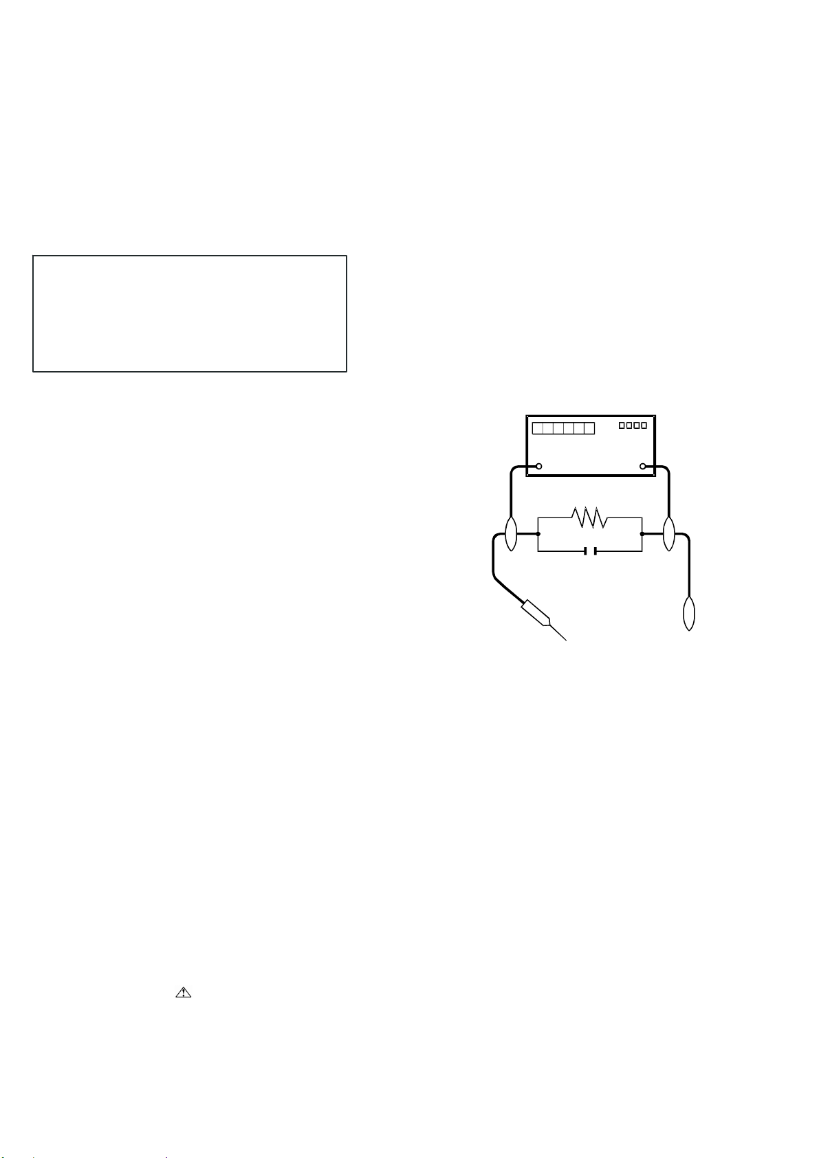
SAFETY NOTICE
Many electrical and mechanical parts in LCD color television have
special safety-related characteristics.
These characteristics are often not evident from visual inspection,
nor
can protection afforded by them be necessarily increased by using
replacement components rated for higher voltage, wattage, etc.
Replacement parts which have these special safety characteristics
are identified in this manual; electrical components having such
features are identified by “ ” and shaded areas in the Replacement
Parts List and Schematic Diagrams.
//////////////////////////////////////////////////////////////////////////////////////////////////////////////////////////////////////////////////////////////////////////////////////////////////////////////////////////////////////////////////
• Use an AC voltmeter having with 5000 ohm per volt, or higher, sen-
sitivity or measure the AC voltage drop across the resistor.
• Connect the resistor connection to all exposed metal parts having a
return to the chassis (antenna, metal cabinet, screw heads, knobs
and control shafts, escutcheon, etc.) and measure the AC voltage
drop across the resistor.
All checks must be repeated with the AC cord plug connection
reversed. (If necessary, a nonpolarized adaptor plug must be used
only for the purpose of completing these checks.)
Any reading of 1.05 V peak (this corresponds to 0.7 mA peak AC.)
or more is excessive and indicates a potential shock hazard which
must be corrected before returning the monitor to the owner.
DVM
AC SCALE
1.5k ohm
10W
0.15 µF
TEST PROBE
TO EXPOSED
METAL PARTS
CONNECT TO KNOWN
EARTH GROUND
For continued protection, replacement parts must be identical to those
used in the original circuit.
The use of a substitute replacement parts which do not have the same
safety characteristics as the factory recommended replacement parts
shown in this service manual, may create shock, fire or other hazards.
2
Page 3

LC-19SH7E/RU, LC-26SH7E/RU, LC-32SH7E/RU, LC-42SH7E/RU
Precautions for using lead-free solder
Using lead-free wire solder
• When fixing the PWB soldered with the lead-free solder, apply lead-free wire solder. Repairing with conventional lead wire solder may cause
damage or accident due to cracks.
As the melting point of lead-free solder (Sn-Ag-Cu) is higher than the lead wire solder by 40 °C, we recommend you to use a dedicated soldering
bit, if you are not familiar with how to obtain lead-free wire solder or soldering bit, contact our service station or service branch in your area.
Soldering
• As the melting point of lead-free solder (Sn-Ag-Cu) is about 220 °C which is higher than the conventional lead solder by 40 °C, and as it has
poor solder wettability, you may be apt to keep the soldering bit in contact with the PWB for extended period of time. However, Since the land
may be peeled off or the maximum heat-resistance temperature of parts may be exceeded, remove the bit from the PWB as soon as you
confirm the steady soldering condition.
Lead-free solder contains more tin, and the end of the soldering bit may be easily corroded. Make sure to turn on and off the power of the bit as
required.
If a different type of solder stays on the tip of the soldering bit, it is alloyed with lead-free solder. Clean the bit after every use of it.
When the tip of the soldering bit is blackened during use, file it with steel wool or fine sandpaper.
• Be careful when replacing parts with polarity indication on the PWB silk.
3
Page 4
LC-32SH25E
CHAPTER 1. OPERATION MANUAL
[1] SPECIFICATIONS
Specification
Item
LCD screen size 19” diagonal 26” diagona 32” diagona
Number of dots
Video Colour System
TV-Standard
TV Function
Backlight life
Viewing angles H : 170° V : 160° H : 160° V : 150° H : 176° V : 176°
Audio amplifier 3W X 2 5W X 2 5W X 2
Speaker (100 mm X 30 mm) X 2
Rear
Receiving
Channel
TV-Tuning System Auto Preset 999 ch, Auto Label, Auto Sort
STEREO/BILINGUAL NICAM/A2
Antenna
RS-232C 3 pin connector(For service only)
SCART 1 SCART (AV input, Y/C input, RGB input, TV output)
SCART 2
(Only for 26” and 32”)
PC IN D-sub 15 pin (AV input), Ø 3.5mm jack (Audio output)
Component YPbPr, RCA pin (L/R)
SPDIF Digital audio output
AUDIO OUT
(Only for 26” and 32”)
AVOUT(Only for 19”)
HDMI 1
Analogue
Digital
VHF/UHF ATV : IRA-E69, DVB-T : E5-E69
CATV S-band, S1–S41ch
19” lCD Colour TV,
model: lC-19SH7E
3,147,264 dots
(1366 X 768 X 3 dots)
PAL/SECAM/NTSC 3.58/NTSC 4.43/PAL 60
CCIR (B/G, I, D/K, L/L’)
DVB-T (2K/8K OFDM)
50,000 hours (at Backlight Standard
position)
UHF/VHF 75 Ω
SCART (AV input, Y/C input, monitor output [analogue source - ATV, SCART 1, SIDE AV; digital source - DTV])
RCA pin (L/R)
26” lCD Colour TV,
model: lC-26SH7E
50,000 hours (at Backlight Standard
position)
32” lCD Colour TV,
model: lC-32SH7E
60,000 hours (at Backlight Standard
position)
HDMI 2(Only for 26” and 32”)
C. I. (Common Interface) EN50221, R206001
Side
OSD language
Power Requirement
Power Consumption
Weight
Operating temperature 0°C to + 40°C
• As a part of policy of continuous improvement, SHARP reserves the righ t to make design and specification changes for product improvement
without prior notice. The performance specification figures indicated are nominal values of production units. There may be some deviations
from these values in individual units.
Headphones Ø 3.5mm jack (Audio output)
AV IN RCA pin (AV input) , RCA pin (L/R), S-VIDEO ([Y/C input], Not available for 19”)
HDMI 3(only for 32”)
English, German, French, Italian, Dutch, Spanish, Greek, Portuguese, Swedish, Finnish,
Russian, Polish, Turkish, Hungarian, Czech, Slovak, Danish, Norwegian, Estonian, Latvian,
Lithuanian, Slovenian, Bulgarian, Croatian, Romanian, Serbian, Ukrainian, Irish
AC 220–240 V, 50 Hz
45W (Standby<0.3W)
(Method IEC60107)
3.8 kg (Without stand),
4.0 kg (With stand)
55W (Standby<0.3W)
(Method IEC60107)
7.3 kg (Without stand),
8.4 kg (With stand)
150W (Standby<0.3W)
(Method IEC60107)
11.0 kg (Without stand),
12.4 kg (With stand)
4
Page 5

[2] OPERATION MANUAL
Remote control unit
(POWER)
Press to turn the LCD TV on or enter standby mode.
(SOURCE)
Select an input source.
0-9 DIGIT BUTTONS
To select a TV channel directly.
EPG
Press this button to display electronic program guide
in DTV mode.
PRE CH
To display the previous selected TV channel.
HDMI
Press this button you could select HDMI (19”) /
HDMI 1(26”, 32”) / HDMI 2 (26”, 32”) / HDMI 3 (32”).
YPbPr
Press this button you could select YPbPr.
VIDEO
Press this button you could select AV / SCART 1
/SCART 2 (26”, 32”)
PC
Press to direct to the PC mode.
(+/-)
Press to adjust the volume.
Press to toggle audio on and off. You can also press
Vol (+/-) to restore the previous volume level.
(Picture format)
Select picture format to Auto / Normal / Zoom 1/ Zoom
2 / Wide.
P (</>)
Press to select the channel.
DUAL
Select MONO, STEREO, DUAL 1 and DUAL 2 for
ATV channel. Select Audio language for DTV channel.
AUDIO (ADJ)
Press to set the LCD TV to a predefined sound setting.
Personal / Music / Speech
VIDEO (ADJ)
Press to set the LCD TV to a predefined picture
setting. Personal / Standard / Vivid / Movie / Eco
SLEEP
Press to turn the LCD TV off within an amount of time.
(10 ~ 120 minutes.)
∧∨<>
Press ∧∨<> to navigate and confirm your selection.
LC-19SH7E/RU, LC-26SH7E/RU, LC-32SH7E/RU, LC-42SH7E/RU
OK
Press to activate a setting.
MENU / EXIT
Press to activate the LCD TV OSD. Press again to exit
the LCD TV OSD.
Display programme infomation, if available.
TELETEXT
Press this button to activate Teletext. Press again to
turn off Teletext.
MIX
Press this button to activate Teletext with TV.
SIZE
Press this button to change the font size: Full screen,
Top half and Bottom half.
SUBPAGE
To select the subpage when the current page contains
subpage(s).
INDEX
Press this button to return to page 100 or the index
page; and then press 0 to 9. The teletext page will be
numbered and added to the page you select or the
secondary item.
SUBTITLE
For DTV, press it to select subtitle setting.
Off / On / On during mute
For ATV, please activate Teletext to select subtitle
page.
HOLD
Press this button to stop the scrolling of pages.
The text decoder stops receiving data.
REVEAL
Reveal hidden information such as answers to a quiz.
ECO
Press buttons to set the picture with less brightness for
saving energy.
PR LIST
Press to display a list of channels. Then press Red
button to select the Digital or Analogue channel list.
FREEZE
Set the still image. Press again to return to normal
screen.
R/G/Y/B (COLOUR BUTTON)
Press buttons to select the pictures with various
colours of text. Different channels display different
functions.
When you are viewing the channel list, press R button
can go to the previous page, and press G can go to
the next page.
2008-03-14
5
Page 6

LC-19SH7E/RU, LC-26SH7E/RU, LC-32SH7E/RU, LC-42SH7E/RU
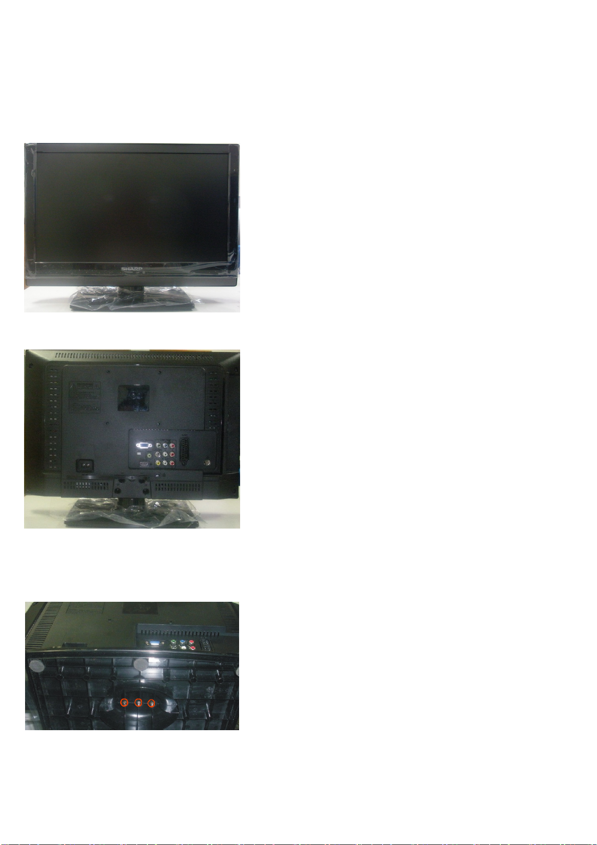
TV (Front view)
TV (Rear view)
6
Page 7

LC-19SH7E/RU, LC-26SH7E/RU, LC-32SH7E/RU, LC-42SH7E/RU
Preparation
Mount the TV Stand
1. Put the TV face down on a safe surface
that is covered by a soft and smooth cloth.
2. Adjust the TV stand to the bottom of the TV.
3. Fasten 4 screws by using a cross-head screwdriver. (Not supplied).
NOTE:
To detach the TV stand, perform the steps in reverse order.
Wall mounting
TV screen size
( inches)
19” 100 x 100 mm Metric 4 x 10 mm
26” 200 x 100 mm Metric 4 x 10 mm
32” 200 x 200 mm Metric 6 x 10 mm
VESA-compatible wall bracket
(millimeters) (W x H)
Screw type
.
2008-03-14
7
Page 8

LC-19SH7E/RU, LC-26SH7E/RU, LC-32SH7E/RU, LC-42SH7E/RU
preparation
Installation of batteries
1. insert two AAA batteries into Remote control.
Make sure (+) and (-) are facing the proper
direction.
2. Replace the cover.
NOTE
• If the remote control will not to be used for a long
time, remove the batteries to avoid remote control damage.
CAUTION
Improper use of batteries can result in chemical leakage or explosion. Be sure to follow the instructions below.
• Do not mix batteries of different types. Different types of batteries have different characteristics.
• Do not mix old and new batteries. Mixing old and new batteries can shorten the life of new batteries or cause
chemical leakage in old batteries.
• Remove batteries as soon as they have worn out. Chemicals that leak from batteries can cause a rash. If you find
any chemical leakage, wipe thoroughly with a cloth.
• The batteries supplied with this product may have a shorter life expectancy due to storage conditions.
• If you will not be using the remote control unit for an extended period of time, remove the batteries from it.
Note on disposing batteries:
The batteries provided contain no harmful materials such as cadmium, lead or mercury.
Regulations concerning used batteries stipulate that batteries may no longer be thrown out with the household
Rubbish. Deposit any used batteries free of charge into the designated collection containers set up at commercial
Businesses.
Using the remote control unit Bundling the cables
Use the remote control unit by pointing it towards the
remote control sensor. Objects between the remote
control unit and sensor may prevent proper operation.
8
Page 9

LC-19SH7E/RU, LC-26SH7E/RU, LC-32SH7E/RU, LC-42SH7E/RU
Appendix
troubleshooting
problem possible Solution
No picture 1. Connect power cord correctly.
2. Turn on power.
3. Connect signal cable correctly.
4. Press any button on the LCD TV.
Abnormal colours Connect signal cable correctly.
Twisted picture 1. Connect signal cable correctly.
2. Please use compatible signal.
Picture too dark Adjust brightness and contrast.
Audio only, no images 1. Please check if input signal is connected correctly.
Picture only, no audio 1. Connect signal cable correctly.
Cannot use remote control 1. Please change battery.
Cannot receive sufficient channels
through antenna
No colours Please adjust the colour setup
Blinking picture accompanied by ghost
image
Broken lines or segments
Certain TV channels are blocked (Hope to
acquire some channels)
Overlapping images or ghost images Please use multi-directional outdoor antenna. (If your TV is subject to the influence of nearby mountains or
Cannot use a function If the item you choose turns gray, that item cannot be selected.
Cannot receive programs Please use the Update scan method to add the channels not included in memory.
1. When a lamp in LCD panel is broken and the
protector circuit in inverter operates and we
tune on the this set, LED keep red? or Green?
2. Service man only change the lamp in LCD
panel?
Cautions regarding use in high and low temperature environments
• When the unit is used in a low temperature space (e.g. room, office), the picture may leave trails or appear slightly delayed. This
is not a malfunction, and the unit will recover when the temperature returns to normal.
• Do not leave the unit in a hot or cold location. Also, do not leave the unit in a location exposed to direct sunlight or near a
heater, as this may cause the cabinet to deform and the LCD panel to malfunction.
• Storage temperature: +5°C to +35°C.
information on the software license for this product
Software composition
The software included in this product is comprised of various software components whose individual copyrights are held by SHARP or by third parties.
Software developed by SHarp and open source software
The copyrights for the software components and various relevant documents included with this product that were developed or written by SHARP are
owned by SHARP and are protected by the Copyright Act, international treaties, and other relevant laws. This product also makes use of freely
distributed software and software components whose copyrights are held by third parties. These include software components covered by a GNU
General Public License (hereafter GPL), a GNU Lesser General Public License (hereafter LGPL) or other license Agreement.
obtaining source code
Some of the open source software licensors require the distributor to provide the source code with the executable software components. GPL and
LGPL include similar requirements. For information on obtaining the source code for the open source software and for obtaining the GPL, LGPL, and
other license agreement information, visit the following website:
2. TV-RF signal must not be lower than 50dB.
2. Adjust volume to proper level.
3. Connect audio signal cable correctly.
4. TV-RF signal must not be lower than 50dB.
2. Turn off power for 10 seconds; and then restart power.
Please use the Channel scan function to increase the number of channels not included in memory.
1. Check the connection of antenna/signal cable.
2. Check if channel is in play mode.
3. Press signal source and change input mode.
Adjust antenna.
Keep the TV away from noise sources, such as automobiles, neon lights, and hair dryers.
Please use the Update scan method to add the channels not included in memory
buildings).
1. If the lamp(s) is(are) broken, panel inverter will not kick on the lamps, so TV set phenomena will be "no picture
on display."
But the TV system is still working, that is the RC can also control LED.
When AC power on, the LED will keep last status and when use RC DC power on, the LED will keep green light.
2. The failed panel should be sent back to Panel maker (CMO) via RMA process.
Panel maker (CMO) will not rework the lamps at customer's side since the repaired panel should be checked
through regular inspection flow to secure the quality.
http://www.sharp-eu.com/gpl/
We are unable to answer any questions about the source code for the open source software. The source code for the software components whose
copyrights are held by SHARP is not distributed.
acknowledgements
The following open source software components are included in this product:
•linuxkernel•modutils•glibc•zlib•libpng
2008-03-14
9
Page 10

LC-19SH7E/RU, LC-26SH7E/RU, LC-32SH7E/RU, LC-42SH7E/RU
[3] DIMENSIONS
10
Page 11
LC-19SH7E/RU, LC-26SH7E/RU, LC-32SH7E/RU, LC-42SH7E/RU
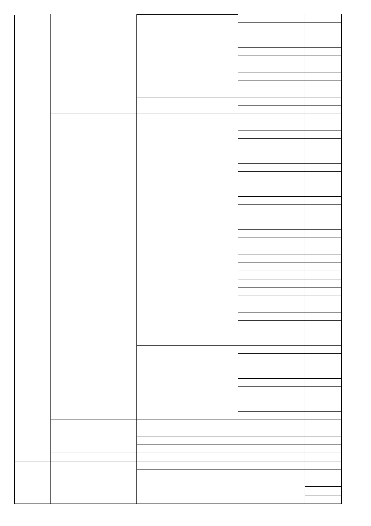
CHAPTER 2. REMOVING OF MAJOR PARTS
[1] REMOVING OF MAJOR PARTS(LC-19SH7E)
1. Assy/Panel Removal
Notes: Please put your machine on soft material to avoid to scrape panel when you disassemble it.
Front view
Fig.1
Back view
Fig.2
Step 1. Remove the Base Assy.
1. Remove the base as Fig.3.
Remove the 3 screws as Fig.3 and pull out the base as Fig.4
Fig.3
2008-03-14
11
Page 12

LC-19SH7E/RU, LC-26SH7E/RU, LC-32SH7E/RU, LC-42SH7E/RU
Fig.4
2. Remove the 4 screws. Detach the Neck as Fig.5.
Step 2. Remove the REAR COVER Assy.
1. Remove the 7 screws. Detach the REAR COVER as Fig.5.
Fig.5
Step 3. Remove the Main and Power board.
Fig.6
1. Remove the 6 screws and disconnect 4 cables. Detach the Main board as Fig.7 and Fig.8.
12
Page 13

Fig.7
LC-19SH7E/RU, LC-26SH7E/RU, LC-32SH7E/RU, LC-42SH7E/RU
Fig.8
2. Remove the 5 screws and disconnect 4 cables. Detach the Power board as Fig.9.
Fig.9
Step 4. Remove the Bezel.
1. Remove the 6 screws. Detach the Bezel as Fig.10.
2008-03-14
13
Page 14

LC-19SH7E/RU, LC-26SH7E/RU, LC-32SH7E/RU, LC-42SH7E/RU
Fig.10
Step 5. Remove the Speakers and Metal Frame.
1. Remove the 4 screws. Detach the Metal Frame and Speakers as Fig.11 and Fig.12.
Fig.11 Fig.12
Panel:
Fig.13
Step 6. Remove the IR and Key board.
1. Remove the 2 screws and disconnect 1 cable. Detach the IR board as Fig.14.
Fig.14
2. Disconnect 1 cable. Detach the Key board as Fig.15.
14
Page 15

LC-19SH7E/RU, LC-26SH7E/RU, LC-32SH7E/RU, LC-42SH7E/RU
Fig.15
2008-03-14
15
Page 16

LC-19SH7E/RU, LC-26SH7E/RU, LC-32SH7E/RU, LC-42SH7E/RU
REMOVING OF MAJOR PARTS(LC-26SH7E)
1. Assy/Panel Removal
Notes: Please put your machine on soft material to avoid to scrape panel when you disassemble it.
Front view
Fig.16
Back view
Fig.17
Step 1. Remove the Base Assy.
1. Remove the base as Fig.18.
Remove the 4 screws as Fig.18 and pull out the base as Fig.19
Fig.18
16
Page 17

Fig.19
2. Remove the 4 screws. Detach the Neck as Fig.19.
Step 2. Remove the REAR COVER Assy.
1. Remove the 7 screws. Detach the REAR COVER as Fig.20.
LC-19SH7E/RU, LC-26SH7E/RU, LC-32SH7E/RU, LC-42SH7E/RU
Fig.20
Step 3. Remove the Main, Power board and the Speakers.
Fig.21
1. Remove the 5 screws and disconnect 4 cables. Detach the Main board as Fig.22 and Fig.23.
2008-03-14
17
Page 18

LC-19SH7E/RU, LC-26SH7E/RU, LC-32SH7E/RU, LC-42SH7E/RU
Fig.22 Fig.23
2. Remove the 5 screws and disconnect 2 cables. Detach the Power board as Fig.24.
Fig.24
3. Remove the 4 screws. Detach the Speakers as Fig.25.
Fig.25
Step 4. Remove the Bracket and Bezel.
1. Remove the 8 screws. Detach the Bracket as Fig.26 and Fig.27.
18
Page 19

Fig.26 Fig.27
2. Remove the 4 screws. Detach the Bezel as Fig.28.
LC-19SH7E/RU, LC-26SH7E/RU, LC-32SH7E/RU, LC-42SH7E/RU
Fig.28
Panel:
Fig.29
Step 5. Remove the IR and Key board.
1. Remove the 2 screws and disconnect 1 cable. Detach the IR board as Fig.30.
2008-03-14
19
Page 20

LC-19SH7E/RU, LC-26SH7E/RU, LC-32SH7E/RU, LC-42SH7E/RU
Fig.30
2. Disconnect 1 cable. Detach the Key board as Fig.31.
Fig.31
2. Set Re-assembly
To re-assemble the whole set, execute all processes in reverse order.
Notes:
a. While re-assembling, make sure that all cables are placed and connected in their original position.
b. Pay special attention not to damage the EMC foams at the SSB shielding. Check that EMC foams are put
correctly on their places.
20
Page 21

LC-19SH7E/RU, LC-26SH7E/RU, LC-32SH7E/RU, LC-42SH7E/RU
CHAPTER 3. ADJUSTMENT PROCEDURE
PROCEDURE
[1] ADJUSTMENT PROCEDURE
1. OSD Menu
2009 SHARP DVB OSD tree-Video
OSD Layer 1 2 3 4 5
Off
Low
Medium
HIGH
Auto
On
Off
On
Off
Smart Picture
Brightness slider
Contrast slider
Color slider
Tint slider
Sharpness slider
Picture
Sound
TV Country(26)
Color Temperature
Advanced Control(have sub page)
Sound Mode
Equilizer 120Hz slider
Equilizer 500Hz slider
Equilizer 1.5KHz slider
Equilizer 5KHz slider
Equilizer 10KHz slider
Balance slider
Virtual Surround
Digital Audio Out
AVL
Type(if source is DTV)
Audio Description(if Type=Audio
Description)
2008-03-14
Personal
Standard
Vivid
Movie
Eco
Normal (default)
Cool
Warm
Noise Reduction
Flesh Tone
Back Light slider
DCR
Personal
Music
Speech
On
Off
PCM
Off
Dolby Digital
Off
On
Normal
Hard of Hearing
Audio Description
Volume slider
UK
Italy
Luxembourg
21
Page 22

LC-19SH7E/RU, LC-26SH7E/RU, LC-32SH7E/RU, LC-42SH7E/RU
Netherlands
Norway
Sweden
Croatia
Hungary
Ireland
Poland
Portugal
Romania
Serbia
Slovakia
Slovenia
Turkey
Iceland
Austria
Belgium
Switzerland
Czech Republic
Germany
Denmark
Spain
Finland
France
English
Finnish
French
Gaelic
Galician
German
Greek
Hungarian
Italian
Norwegian
Polish
Portuguese
Romanian
1st Audio(28)(DTV only)
2nd Audio(28)(DTV only)
Russian
Serbian
Slovak
Slovenian
Spanish
Swedish
Turkish
Welsh
Basque
Bulgarian
Catalan
Croatian
Czech
Danish
Dutch
English
Finnish
French
Gaelic
Galician
German
Greek
Hungarian
Italian
22
Page 23

Channels(have sub page)
Features Menu Language(24)
2008-03-14
LC-19SH7E/RU, LC-26SH7E/RU, LC-32SH7E/RU, LC-42SH7E/RU
Norwegian
Polish
Portuguese
Romanian
Russian
Serbian
Slovak
Slovenian
Spanish
Swedish
Turkish
Welsh
Basque
Bulgarian
Catalan
Croatian
Czech
Danish
Dutch
Channel Scan
Update Scan
Single RF Scan
Analog Manual Scan
Channel Skip(have sub page) (Channel munber…)
Channel Sort(have sub page) (Channel munber…)
Channel Edit(have sub page) (Channel munber…)
Decoder(for ATV) (Channel munber…)
Analog Ch Fine Tune
English
Deutsch
Français
Italiano
Español
Português
Nederlands
Български
Dansk
Suomi
Svenska
Norsk
Polski
Русский
Česky
Hrvatski
Magyar
Română
Slovenský
Slovenščina
Srpski
Türkçe
Ελληνικά
Status: scanning…
Analogue channels:
Digital channels:
Status: scanning…
Analogue channels:
Digital channels:
RF Channel ..
Signal Strength..
Signal Quailty..
Start Frequency xxMHz
Scan Up
Scan Down
(Channel munber…)(have
sub page)
(do fine tune)
23
Page 24

LC-19SH7E/RU, LC-26SH7E/RU, LC-32SH7E/RU, LC-42SH7E/RU
Gaeilge
Latvian
Estonian
Lithuanian
Ukrainian
Auto
Normal
Picture Format
Time (have sub page )
Zoom1
Zoom2
Wide
Time Zone
Time(have sub page)
Sleep Timer
As Broadcaster
GMT +0:00
GMT +1:00
GMT +2:00
GMT +3:00
GMT +3:30
GMT +4:00
GMT +4:30
GMT +5:00
GMT +5:30
GMT +5:45
GMT +6:00
GMT +6:30
GMT +7:00
GMT +8:00
GMT +9:00
GMT +9:30
GMT +10:00
GMT +11:00
GMT +12:00
GMT +12:45
GMT +13:00
GMT -12:00
GMT -11:00
GMT -10:00
GMT -9:00
GMT -8:00
GMT -7:00
GMT -6:00
GMT -5:00
GMT -4:00
GMT -3:30
GMT -3:00
GMT -2:00
GMT -1:00
Auto synchronization
( On/Off)
Date ( 20xx/xx/xx )
Time ( xx:xx:xx)
Timer (Off/On)
Off Time ( xx:xx:xx)
Off
10 Min
20 Min
30 Min
40 Min
50 Min
60 Min
90 Min
120 Min
24
Page 25

SCART(have sub page)
(Only availabe in SCART source)
Subtitle(have sub page)
2008-03-14
LC-19SH7E/RU, LC-26SH7E/RU, LC-32SH7E/RU, LC-42SH7E/RU
SCART2(If have I/O)
Analog Subtitle
1st Subtitle(28)
2nd Subtitle(28)
SCART1
Auto
Mixed
RGB
Composite
S-Video
Auto
Composite
S-Video
On
On during mute
Off
English
Finnish
French
Gaelic
Galician
German
Greek
Hungarian
Italian
Norwegian
Polish
Portuguese
Romanian
Russian
Serbian
Slovak
Slovenian
Spanish
Swedish
Turkish
Welsh
Off
Basque
Bulgarian
Catalan
Croatian
Czech
Danish
Dutch
English
Finnish
French
Gaelic
Galician
German
Greek
Hungarian
Italian
Norwegian
Polish
Portuguese
Romanian
Russian
Serbian
Slovak
Slovenian
Spanish
Swedish
25
Page 26
LC-19SH7E/RU, LC-26SH7E/RU, LC-32SH7E/RU, LC-42SH7E/RU
Subtitle Type
Digital Teletext Lang.
Teletext Language(have sub page)
Decode Page Lang.
Common Interface(have sub page) (display some info & status..)
HDMI Scan Info
(Only available in HDMI source)
Reset Default
Parental Password(have sub page)
Automatic
Underscan
Overscan
Channel Block(have sub page) (Channel munber…)
Parental Guidance(have sub page) Age Rating
Turkish
Welsh
Off
Basque
Bulgarian
Catalan
Croatian
Czech
Danish
Dutch
Normal
Hearing Impaired
English
Spanish
French
German
Italian
Danish
Swedish
Basque
Bulgarian
Catalan
Croatian
Czech
Dutch
Finnish
Gaelic
Galician
Greek
Hungarian
Norwegian
Polish
Portuguese
Romanian
Russian
Serbian
Slovak
Slovenian
Turkish
Welsh
WEST EUR
EAST EUR
Russia
Russia-2
Greek
Turkey
Arab/Hbrw
Farsian
Arab
18
None
4
5
26
Page 27

LC-19SH7E/RU, LC-26SH7E/RU, LC-32SH7E/RU, LC-42SH7E/RU
Input Block(have sub page) (Source list..)
Set password (have sub page)
Clear All
Off
Eco
On
New Password (xxxx)
Confirm Password (xxxx)
2009 SHARP DVB OSD tree-PC
OSD Layer 1 2 3 4 5
Brightness slider
Contrast slider
Normal (default)
Color Temperature
Advanced Video(have sub page)
Audio Mode
Equilizer 120Hz slider
Equilizer 500Hz slider
Equilizer 1.5KHz slider
Equilizer 5KHz slider
Sound
Features Menu Language(24)
Equilizer 10KHz slider
Balance slider
Virtual Surround
Digital Audio Out
AVL
2008-03-14
Cool
Warm
Auto Config Auto Config
Horizontal slider
Vertical slider
Phase slider
Clock slider
Resolution list all ambiguous timings
Personal
Music
Speech
On
Off
PCM
Off
Dolby Digital
Off
On
English
Deutsch
Français
Italiano
Español
Português
Nederlands
Български
Dansk
Suomi
Svenska
Norsk
Polski
Русский
Česky
27
6
7
8
9
10
11
12
13
14
15
16
17
Page 28

LC-19SH7E/RU, LC-26SH7E/RU, LC-32SH7E/RU, LC-42SH7E/RU
Hrvatski
Magyar
Română
Slovenský
Slovenščina
Srpski
Türkçe
Ελληνικά
Gaeilge
Latvian
Estonian
Lithuanian
Ukrainian
Picture Format
Reset Default
Parental Password(have sub page)
Eco
Off
On
Full screen
4:3
Parental Guidance (have sub page) Age Rating
Input Block(have sub page) (Source list..)
Set Password(have sub page)
Clear All
18
None
4
5
6
7
8
9
10
11
12
13
14
15
16
17
New Password (xxxx)
Confirm Password (xxxx)
28
Page 29

LC-19SH7E/RU, LC-26SH7E/RU, LC-32SH7E/RU, LC-42SH7E/RU
2. Display adjustment
YPbPr Mode display adjustment
1) Auto color for signal slicering
General set-up :
Equipment Requirements: Minolta CA-110 or Equivalent Color analyzer, Quantum Data Pattern Generator 802G , 802BT or equivalent instrument
Input requirements:
Input Signal Type: YPbPr signal
1>. 1080i/25mode, TVBar100 pattern by 802G or 802BT.
2>. Select Picture mode to User mode and check the x, y data.
Input Signal Strength : 1 Vpp for Y signal ; 700 mVpp for Pb & Pr signal
Input Injection Point : YPbPr (RAC jack)
1080i/25, TVBar100 pattern
Alignment method:
Initial Set-up:
1>. Select source as “YPbPr”.
2.> Set Smart Picture mode as “Personal” and then adjust Contrast = 58, Brightness=48, Color=58, set Color Temp. to be “cool” mode.
3>. Apply “TVBar100” pattern which is color bar pattern by signal generator.
4>. Enter “factory mode menu”: press MENU + Numeric keys “1999”
Alignment:
1>. At factory mode menu, select AUTO_COLOR item. Then press “OK” key of remote control to adjust ADC_GAIN_R, ADC_GAIN_G, ADC_GAIN_B and
ADC_OFFSET_R, ADC_OFFSET_G, ADC_OFFSET_B. Then store those values to NVM.
2>. Check the 16 grayscale pattern should be distinguished and color bar is correct
3>. Reset AV setting, picture mode shall be recalled to be “Vivid” and Contrast=58, Brightness=48; Color=58.
2) White balance adjustment
Alignment method:
Initial Set-up:
1>. Select source as “YPbPr”.
2>. Set Contrast = 58 and Brightness=48, Color=58, at normal menu mode.
3>. Apply “80% white pattern or Flat 80 pattern by Component video generator.
4>. Enter factory mode menu: press MENU + Numeric keys 1999”.
Alignment:
1>. Apply Flat80 pattern (80% white pattern).
2>. Set color temperature to “NORMAL”.
3>. At factory mode menu, adjust the CLR TEMP R
store those values to NVM
4>. Set color temperature to “COOL”.
2008-03-14
, CLR TEMP G, CLR TEMP B values to meet “NORMAL” color coordinates specification below. Then
29
Page 30

LC-19SH7E/RU, LC-26SH7E/RU, LC-32SH7E/RU, LC-42SH7E/RU
5>. At factory mode menu, adjust the CLR TEMP R, CLR TEMP G, CLR TEMP B values to meet “COOL” color coordinates specification below. Then
store those values to NVM
6>. Set color temperature to “WARM”.
7>. At factory mode menu, adjust the CLR TEMP R
store those values to NVM
Color temperature Normal/Warm/Cool (x, y) co-ordinates specification:
Note:
1>. Use Minolta CA-210 for color coordinates and luminance check.
2>. Befor adjusting,all colour analyzers (CA-210) should be coordinates with a same reference TV set.
3>. Check the luminance in the center of the screen with 100% White when Brightness control at 100; Contrast control at 100
Luminance > 230 cd/m
> 350 cd/m
> 400 cd/m
2
<< For 19” only at color temp.- warm mode >>
2
<< For 26” only at color temp.- cool mode >>
2
<< For 32” only at color temp.- cool mode >>
Picture Mode x y
Normal (9000oK) 0.289±0.003 0.291±0.003
Cool (12000oK) 0.272±0.003 0.277±0.003
Warm (6500oK) 0.314±0.003 0.319±0.003
, CLR TEMP G, CLR TEMP B values to meet “WARM” color coordinates specification below. Then
Reading with Minolta CA-210.
PC mode display adjustment
1) Auto color for signal slicering
General set-up :
Equipment Requirements: Minolta CA-210 or Equivalent Color analyzer, Chroma 2250 or equivalent PC signal generator
Input requirements:
Input Signal Type : PC VGA signal
1>. 1280X1024/60Hz PC mode with “5 white block” pattern. (see pattern-1)
Input Signal Strength : 0.7 Vp-p linear voltage.
Input Injection Point : PC D-SUB input
Pattern-1
Alignment method:
Initial Set-up:
1>. Select source as “PC”.
2>. Set Contrast = 50 (Sharp) and Brightness=50 (Sharp) , at normal menu mode.
3>. Apply “5 white block”(pattern-1) pattern by VGA pattern generator.
4>. Enter factory mode menu: press MENU + Numeric keys “1999” (factory mode menu).
Alignment:
1>. At factory mode menu, select AUTO_COLOR item. Then press “OK” key to adjust ADC_GAIN_R, ADC_GAIN_G, ADC_GAIN_B and
ADC_OFFSET_R, ADC_OFFSET_G, ADC_OFFSET_B. Then store those values to NVM.
Check color temperature specification with PC mode.
Color temperature Normal/Warm/Cool (x, y) co-ordinates specification:
30
Page 31

LC-19SH7E/RU, LC-26SH7E/RU, LC-32SH7E/RU, LC-42SH7E/RU
Note:
1. Use Minolta CA-210 for color coordinates and luminance check.
2. Befor checking,all colour analyzers (CA-210) should be coordinates with a same reference TV set.
3. Check the luminance in the center of the screen with 100% White when Brightness control at 100; Contrast control at 100
Luminance > 230 cd/m
> 350 cd/m
> 400 cd/m
2
<< For 19” only at color temp.- warm mode >>
2
<< For 26” only at color temp.- cool mode >>
2
<< Foolor temp.- cool mode >>
Picture Mode x y
Normal (9000oK) 0.289±0.015 0.291±0.015
Cool (12000oK) 0.272±0.010 0.277±0.010
Warm (6500oK) 0.314±0.015 0.319±0.015
Reading with Minolta CA-210.
3. Factory mode preset.
Default Values
VIRGIN_MODE On
GAMMA_TABLE
COLOR_ENHANCE On
Note: VIRGIN_MODE is ON for outging and is Off at production line.
YPbPr PC
ADC_GAIN_R 64 64
ADC_GAIN_G 64 64
ADC_GAIN_B 64 64
ADC_OFFSET_R 128 128
ADC_OFFSET_G 128 128
ADC_OFFSET_B 128 128
Note: These above values will be changed after doing “AUTO_COLOR” at FAC mode menu.
PC
NORMAL COOL WARM
CLR_TEMP_R 0 0 0
CLR_TEMP_G 0 0 0
CLR_TEMP_B 0 0 0
Note: These above values will be changed after doing W/D alignment at FAC mode menu
TUNER_ID 4 (Panasonic ENG37E14KRF)
PANEL_ID 110: for CMO 19” panel 122: for CMO 26” panel 33: for Sharp 32” panel
These above values are defined by Development Division and written in release NVM.
2008-03-14
31
Page 32

LC-19SH7E/RU, LC-26SH7E/RU, LC-32SH7E/RU, LC-42SH7E/RU
[2] SERVICE MODE
Enter factory mode menu: press MENU + Numeric keys “1999” to enter factory mode.
32
Page 33

LC-19SH7E/RU, LC-26SH7E/RU, LC-32SH7E/RU, LC-42SH7E/RU
[3] SOFTWARE UPGRADE PROCEDURE
Environment Setup
Before you start to write the code, we suggest you setup the environment first. This chapter lists the setup requirements and guides you to setup and test
your development environment.
Connect to TV USB port to upgrade the software firmware
Please follow the following step to upgrade the firmware.
1. Copy the software firmware (*.pkg) to USB Disk.
2. Modify the pkg’s filename to “upgrade.pkg”
3. Insert the USB Disk to TV USB port.
4. TV AC power off -> AC power on
5. TV will upgrade after detect the USB disk condition and the content of the pkg file.
Select “Yes” , then press “>” on the remote control, TV will upgrade the software by itself.
6. After finish upgrade process, Press “
” on the remote control to turn off the TV.
2008-03-14
33
Page 34

LC-19SH7E/RU, LC-26SH7E/RU, LC-32SH7E/RU, LC-42SH7E/RU
7. Remove USB disk from TV.
8. Check the software version is correct or not.
(MENU / Features)
34
Page 35

LC-19SH7E/RU, LC-26SH7E/RU, LC-32SH7E/RU, LC-42SH7E/RU
p
CHAPTER 4. TROUBLESHOOTING TABLE
[1] 19” TROUBLESHOOTING TABLE
Power unit operation check.
↓
Are the power cord and harness in the unit properly connected?
LINE_FILTER_UNIT: ↓ YES
Is F901 normal?
POWER_UNIT
Is BD901 (+320V) output?
* When power on/off switch is on ‧‧‧ About +400V
↓YES
↓YES
Is a voltage of +5.3V applied to pin (3,4) of connector (CN902)?
↓YES
Is a voltage of +18V applied to pin (8,9) of connector (CN902)?
NO
NO
NO
NO
NO
Connect the power cord and harness properly, and turn on the
ower.
LINE_FILTER_UNIT:
Isn't C908, RV901, L902, C900, C901, etc. out of order?
Moreover, whether the short-circuit with the circumference circuit
is checked.
Does the circuit operate normally?
Check circuit around (FB901, Q906, ZD904, IC901 etc ).
Does the switching circuit operate normally?
Check circuit around the primary side (T901, ZD906, D901,
D903, Q903, D904, IC901, IC902, D905 etc.), the secondary
side (D905, L904, etc.), the DC_DET circuit (IC902, ZD903,
IC901, ZD902, etc.), and the protection circuit.
Does the inverter circuit operate normally?
Check circuit around (Q801, ZD801, ZD802, Q805, Q806, IC801,
T801, L801, L802, etc.), and the protection circuit.
2008-03-14
35
Page 36

LC-19SH7E/RU, LC-26SH7E/RU, LC-32SH7E/RU, LC-42SH7E/RU
The sound is not emitted from the speaker though the picture has come out.
↓
No sound output in all modes?
TEREMINAL UNIT: ↓
Is the audio signal output of pin (H26) (AL0) and pin (H25) (AR0) of
IC U400 normal?
NO
↓YES
Is the audio signal output of pin (17) (PGA2OUTL) and pin (18)
(PGA2OUTR) of IC U605 normal?
NO
↓YES
Is audio signal input to pin (2)(L), pin (14)(R) of IC U600 (AMP)?
NO
↓YES
Is MUTE circuit [AMP_MUTE_LINE, POWERUP_LINE] normal?
NO
↓YES
Is the audio signal output of pin (3, 4) (L-ch) and pin (1, 2) (R-ch) of
CN600 (AOUDIO-CONNECTOR) normal?
NO
↓YES
Check Speaker Box (right and left) and wire harness.
No sound (during the reception of TV(ANALOG) broadcasting)
↓
Does not the sound go out though the picture has come out when UHF/VHF is received?
TEREMINAL UNIT: ↓
Is the SIF signal output from pin (11) of TUNER (TU201)?
NO
↓YES
Is the SIF signal sent to pin (AB25) and pin (AB26) of IC U400?
NO
↓YES
Refer to “No sound output in all modes”.
Check IC U400 and its peripheral circuits.
Check IC U605 and its peripheral circuits.
Check the line between IC U605 and IC U600.
Check the AMP_MUTE_LINE and POWERUP_LINE. (Q600,
etc.)
Check IC U600 and its peripheral circuits.
Check the tuner and its peripheral circuits. Replace as required.
Check IC U400 its peripheral circuits.
36
Page 37

LC-19SH7E/RU, LC-26SH7E/RU, LC-32SH7E/RU, LC-42SH7E/RU
No sound (during the reception of TV (DIGITAL) broadcasting)
↓
Does not the sound go out though the picture has come out when DTV is received?
MAIN UNIT: ↓
Is the DIF signal output from pin (20) and pin (21) of TUNER
(TU201)?
NO
↓YES
Is the DIF signal sent to pin (R25) and pin (T25) of IC U400?
NO
↓YES
Refer to “No sound output in all modes”.
No sound from external input devices (1)
↓
Does not the sound of the audio signal input to SCART1 go out?
TEREMINAL UNIT: ↓
Is the audio signal properly sent to pin (6) (SCT1_AUL_IN) and pin
(2) (SCT1_AUR_IN) of SCART1(CN500)?
NO
↓YES
Is the audio signal properly sent to pin (44) (SC1_LIN) and pin (43)
(SC1_RIN) of IC U605?
NO
↓YES
Refer to “No sound output in all modes”.
No sound from external input devices (2)
↓
Does not the sound of the audio signal input to AV1(Component) go out?
MAIN UNIT: ↓
Is the audio signal properly sent to pin (2) (AV1_AudioLIN) and pin
(4)(AV1_AudioRIN) of CN557?
NO
↓YES
Is the audio signal properly sent to pin (50) (AV1_LIN) and pin (49)
(AV1_RIN) of IC U605?
NO
↓YES
Refer to “No sound output in all modes”.
Check the tuner and its peripheral circuits. Replace as required.
Check IC U400 its peripheral circuits.
Check the setting of an external input device that connects of
CN500.
Check the line between CN500 and IC U605.
Check the connection to CN557 and the external input device.
Check the line between CN557 and IC U605.
2008-03-14
37
Page 38

LC-19SH7E/RU, LC-26SH7E/RU, LC-32SH7E/RU, LC-42SH7E/RU
No sound from external input devices (3)
↓
Does not the sound of the audio signal input to AV3(Composite) go out?
MAIN UNIT: ↓
Is the audio signal properly sent to pin (4) (AV3_AudioLIN) and pin
(6) (AV3_AudioRIN) of CN650?
NO
↓YES
Is the audio signal properly sent to pin (52) (SIDE_LIN) and pin (51)
(SIDE_RIN) of IC U605?
NO
↓YES
Refer to “No sound output in all modes”.
No sound from external input devices (4)
↓
Does not the sound of the audio signal input to VGA go out?
MAIN UNIT: ↓
Is the audio signal properly sent to pin (2) (VGA_AudioLIN) and pin
(3) (VGA_AudioRIN) of CN555?
NO
↓YES
Is the audio signal properly sent to pin (48) (VGA_LIN) and pin (47)
(VGA_RIN) of IC U605?
NO
↓YES
Refer to “No sound output in all modes”.
No sound from external input devices (5)
↓
Does not the sound of the audio signal input to HDMI go out?
↓
Is picture of the signal input from HDMI displayed?
NO
↓YES
Refer to “No sound output in all modes”.
Check the connection to CN650 and the external input device.
Check the line between CN650 and IC U605.
Check the connection to CN555 and the external input device.
Check the line between CN555 and IC U605.
Refer to “Does not the picture of the HDMI signal input to HDMI
go out?”.
38
Page 39

The audio signal is not output (1)
↓
The audio signal of UHF/VHF is not output from SCART1.
TEREMINAL UNIT: ↓
Is audio signal output from IC U602 sent to pin (3)(SCT1_AULOUT) and pin(1)(SCT1_AUR-OUT) of SCART1(CN500)?
↓NO
Is audio signal output from IC U400 sent to pin (2)(LRCLK) and pin
(3)(DIN) and pin (4)(BCLK) and pin(13)(MCLK) of IC U602?
↓NO
Check IC U400 and its peripheral circuits.
The audio signal is not output (2)
↓
No audio signal output from LINE_AUDIO_OUTPUT terminal.
TEREMINAL UNIT: ↓
Is audio signal output from IC U605 sent to pin(4)(AUL_OUT) and
pin (6)(AUR_OUT) of LINE_AUDIO_OUT connector(CN501)?
↓NO
Is the audio signal output from IC U400 pin(K26) (AL2) and pin(J24)
(AR2) sent to pin(26)(INPUT1L) and pin(25)(INPUT1R) of IC U605?
↓NO
Check IC U400 and its peripheral circuits.
LC-19SH7E/RU, LC-26SH7E/RU, LC-32SH7E/RU, LC-42SH7E/RU
YES
Check the connection to SCART1 and external devices.
YES
Check the line between IC U400 and IC U602.
YES
YES
Check the connection to LINE_AUDIO_OUT and external
devices.
Check the line between IC U400 and IC U605.
2008-03-14
39
Page 40

LC-19SH7E/RU, LC-26SH7E/RU, LC-32SH7E/RU, LC-42SH7E/RU
The audio signal is not output (3)
↓
No audio signal output from SPDIF_OUTPUT terminal.
TEREMINAL UNIT: ↓
Is ASPDIF audio signal output from pin (E26) of IC U400 to pin (6)
of connector CN556?
YES
↓NO
Check IC U400 and its peripheral circuits.
The audio signal is not output (4)
↓
No sound from HEADPHONE_OUTPUT terminal.
MINI AV_UNIT: ↓
Is the HPDET signal input into pin (AA5) of IC U400 from pin (6) of
a headphone terminal (CN602)?
NO
↓YES
Is the audio signal output from IC U605 to pin(2) (HPOUTL) and pin
(3) (HPOUTR) of headphone terminal CN602?
NO
↓YES
Is the audio signal output from IC U400 pin(J26)(AL1) and pin(J25)
(AR1) sent to pin(24)(INPUT0L) and pin(23)(INPUT0R) of IC U605?
NO
↓YES
Check IC U400 and its peripheral circuits.
Check the connection to SPDIF_OUT and external devices.
Check the connection to CN602 and external headphone is plug
in well.
Check the line between IC U605 and CN602.
Check the line between IC U400 and IC U605.
40
Page 41

LC-19SH7E/RU, LC-26SH7E/RU, LC-32SH7E/RU, LC-42SH7E/RU
No picture on the display (1)
↓
The picture doesn't appear in all modes.
MAIN UNIT: ↓
Is LVDS signal output from 1st_channel and 2nd_channel of IC U400 in each mode?
(A0N/A0P),(A1N/A1P),(A2N/A2P),(A3N/A3P),(CK1N/CK1P)
↓NO
YES
Is the above-mentioned LVDS signals output to connector CN751?
NO
↓YES
Is LCD controller's control signal normal?
NO
PANEL_UNIT:
Similarly, is the LVDS signal input to connector of the panel
↓YES
NO
↓YES
Check the panel module.
No picture on the display (2)
↓
Does not the picture come out when VHF/UHF is received?
TERMINAL UNIT: ↓
Is TUNER_CVBS signal output from pin (24) of TUNER (TU201)?
NO
MAIN_UNIT: ↓YES
Is picture signal input from pin (24) of TUNER (TU201) to pin
(AB24) of IC U400?
NO
↓YES
Refer to “The picture doesn't appear in all modes.”
Check IC U400 and its peripheral control circuits.
Check the line between IC U400 and CN751.
Control signals BRIGHT_ADJ, INVERTER_ON_OFF,
PANEL_VCC_ON/OFF, and it peels off and whether normality is
checked.
Wire harness is checked.
Check whether I2C is normally accessed between TU201 and IC
U400.
Check the line between IC U400 and TU201.
2008-03-14
41
Page 42

LC-19SH7E/RU, LC-26SH7E/RU, LC-32SH7E/RU, LC-42SH7E/RU
No picture on the display (3)
↓
Does not the picture come out when DTV is received?
TERMINAL UNIT: ↓
Is the voltage of regulation for a TUNER circuit and the power
supply terminal of IC U400 supplied?
↓YES
Is IF signal output from pin (20), (21) of TUNER (TU201) to pin
(R25), pin (T25) of IC U400 ?
NO
NO
↓YES
Is MPEG data (TS0INDATA0, TS0INSYNC, TS0INCLK,
TS0INVALID) from IC U400 are output to pin (9), pin (7), pin (6), pin
(8) of a IC U401?
MAIN_UNIT:
Do X300 (60.00MHz)/ X400 (27MHz) oscillate?
↓YES
Is MPEG data (TS_DATAO, TS_CKO, TS_VALIDO, TS_SYNCO)
from IC U401 are output to pin (B21/A21/B20/C21) of a IC U400?
↓YES
NO
NO
NO
↓YES
Refer to “The picture doesn't appear in all modes.”
<External input SCART1>No picture on the display (4)
↓
Does not the picture of the CVBS signal input to SCART1 go out?
TERMINAL UNIT: ↓
Is CVBS signal sent to pin (20) of SCART1 (CN500)?
NO
MAIN_UNIT: ↓YES
Is CVBS signal sent to pin (AE24) of IC U400?
Refer to “The picture doesn't appear in all modes.”
↓YES
NO
Each power supply circuit is checked.
Check the tuner, IC U400 and their peripheral circuits. Replace
as required.
is communication control carried out between pin (12)(SCL),
pin(13)(SDA), of TU201, and pin(F24)(TUNER_SCL1), pin
(F25)(TUNER_SDA1), of IC U400?
Check X300/ X400 and its peripheral circuits.
Is the control signal between IC U401 and IC U400 normal?
(RESET_CI, etc.).
Check the setting of an external input device that connects of
CN500.
Check the line between IC U400 and CN500.
42
Page 43

LC-19SH7E/RU, LC-26SH7E/RU, LC-32SH7E/RU, LC-42SH7E/RU
<External input SCART1>No picture on the display (5)
↓
Does not the picture of the R/G/B video signal input to SCART1 go out?
TERMINAL UNIT: ↓
Is RGB signal sent to pin (15)/R, (11)/G, (7)/B, of SCART1
(CN500)?
MAIN_UNIT:
Is RGB signal sent to pin (AF24)/R, (AD24)/G, (AD23)/B of IC
U400?
Refer to “The picture doesn't appear in all modes.”
↓YES
↓YES
NO
NO
<External input SCART1 >No picture on the display (6)
↓
Does not the picture of the Y/C signal input to SCART1 go out?
TERMINAL UNIT: ↓
Is Y/C signal sent to pin (20) and (15) of SCART1 (CN500)?
MAIN_UNIT:
Is Y/C signal sent to pin (AE24)/Y, (AF25)/C of IC U400?
Refer to “The picture doesn't appear in all modes.”
↓YES
↓YES
<External input AV3(Composite)>No picture on the display (7)
NO
NO
↓
Does not the picture of the composite video signal input to AV3(Composite) go out?
TERMINAL UNIT: ↓
Is CVBS signal sent to pin (2) of AV3 (CN650) ?
NO
MAIN_UNIT: ↓YES
Is CVBS signal sent to pin (AC24) of IC U400?
Refer to “The picture doesn't appear in all modes.”
↓YES
NO
Check the setting of an external input device that connects of
CN500.
Check the line between IC U400 and CN500.
Check the setting of an external input device that connects of
CN500.
Check the line between IC U400 and CN500.
Check the setting of an external input device that connects of
CN650.
Check the line between IC U400 and CN650.
2008-03-14
43
Page 44

LC-19SH7E/RU, LC-26SH7E/RU, LC-32SH7E/RU, LC-42SH7E/RU
)
<External input HDMI1>No picture on the display (8)
↓
Does not the picture of the HDMI signal input to HDMI1 go out?
MINI AV_UNIT: ↓
Is the HOT_PLUG detection function of pin (19) of a HDMI terminal
(CN700) normal?
NO
Check the line between pin (AB5) of IC U400 and CN700.
Check the connection and setup with the external HDMI devices.
YES
Are EDID data pin (6)(SCL) of IC U701 (EEPROM), pin (5)(SDA)
accessed, and is it read from pin (15), pin (16) of a HDMI
terminal(CN700)?
Is TMDS signal input into pin(AF18, AE18)/RX2±,(AF17,
/RX1±, (AF16, AE16)/RX0±, (AF15, AE15)/RXC± of IC U400?
AE17
Refer to “The picture doesn't appear in all modes.”
YES
↓YES
<External input VGA>No picture on the display (9)
NO
NO
Is access possible in the re-writing or exchange of EDID data of
IC U701?
Check CN700, IC U701 and peripheral circuits.
Check the line between IC U400 and CN700.
↓
Does not the picture of the PC IN(ANALOG) video signal input to VGA(15pin-D-SUB terminal) go out?
TERMINAL_UNIT: ↓
Is R/G/B/H/V signal sent to pin (1)/R, (2)/G, (3)/B, (14)/H, (13)/V of
VGA (CN554)?
MAIN_UNIT: ↓YES
Is R/G/B/H/V signal sent to pin (AE20)/R, (AE19)/G, (AD19)/B,
(AC18)/H, (AB18)/V of IC U400?
NO
NO
Check the setting of an external input device that connects of
CN554.
Check the line between IC U400 and CN554.
↓YES
Refer to “The picture doesn't appear in all modes.”
↓
↓NO
44
Page 45

LC-19SH7E/RU, LC-26SH7E/RU, LC-32SH7E/RU, LC-42SH7E/RU
p
)
<External input AV1(Component)>No picture on the display (10)
↓
Does not the picture of the component video signal input to Component go out?
TERMINAL_UNIT: ↓
Is Component Y/Pb/Pr signal sent to pin (2)/Y, (4)/Pb, (6)/Pr of
AV1(CN552) ?
MAIN_UNIT: ↓YES
Is Component Y/Pb/Pr signal sent to pin (AE21)/Y, (AD22)/Pb,
(AF22)/Pr of IC U400?
NO
NO
Check the setting of an external input device that connects of
CN552.
Check the line between IC U400 and CN552.
↓YES
Refer to “The picture doesn't appear in all modes.”
< During external connection > No picture on the monitor (1)
↓
No picture appears on SCART1 - connected monitor during the tuner (U/V) reception.
↓
Checklist:
1) Is the Signal Type (item) in MENU-Option-Input Select equal to Signal Type of an external device? …Set it to “CVBS”, “Y/C”, “RGB”, “AUTO”.
2) Is ANT-CABLE disconnected or connected improperly? …Connect it correctly as per the operation manual.
3) The picture is sent to the monitor in a CVBS signal if the source during display is ATV/DTV, CVBS or Y/C of SCART1, AV3.
When sent by component, etc., that signal is not sent to the monitor.
4) When the monitor picture is not sent and is not displayed on the monitor, refer to “No picture” for each terminal.
5) The video output from SCART1 is not the monitor output (output of the picture now watching).
The
icture of the last selected TV channel is always sent to SCART1. (Specification
TERMINAL_UNIT:
Is CVBS signal output into pin (19) of CN500 (SCART1)?
↓NO
Is TUNER_CVBS signal output into pin (21) of CN500 (SCART1)?
↓
YES
YES
Check the setting of an external input device that connects of
CN500.
Check the line between CN500 and TU200.
↓NO
Refer to “The picture doesn't appear in all modes.”
2008-03-14
45
Page 46

LC-19SH7E/RU, LC-26SH7E/RU, LC-32SH7E/RU, LC-42SH7E/RU
p
)
< During external connection > No picture on the monitor (2)
AVOUT: ↓
No picture from SCART1 appears on AVOUT-connected monitor.
NOTE: Normally, if the screen during display is sent to SCART1, no picture is sent to AVOUT.
↓
Checklist:
1) Is the Signal Type (item) in MENU-Option-Input Select equal to Signal Type of an external device? …Set it to “CVBS”, “Y/C”, “AUTO”.
2) The picture is sent to the monitor in a CVBS signal if the source during display is TV, CVBS or Y/C of SCART1, AV3.
When sent by component, etc., that signal is not sent to the monitor.
3) When the monitor picture is not sent and is not displayed on the monitor, refer to “No picture” for each terminal.
4) The video output from SCART1 is not the monitor output (output of the picture now watching).
The
TERMINAL_UNIT:
Is CVBS signal output into pin (2) of CN501?
↓NO
Is CVBS signal output from pin (A13) of IC U400 into pin (2) of
CN501 ?
icture of the last selected TV channel is always sent to SCART1. (Specification
↓
YES
YES
Check the setting of an external input device that connects of
CN501.
Check the line between CN501 and IC U400.
↓NO
Refer to “The picture doesn't appear in all modes.”
46
Page 47

26” TROUBLESHOOTING TABLE
p
Power unit operation check.
↓
Are the power cord and harness in the unit properly connected?
LINE_FILTER_UNIT: ↓ YES
Is F901/F902 normal?
POWER_UNIT
Is BD901 (+320V) output? (Set the main power SW to OFF.)
* When power on/off switch is on ‧‧‧ About +400V
Is a voltage of +5V applied to pin (12,13) of connector (CN902)?
(Set the main power SW to OFF.)
Are +24V output as for the power on/off switch when it is on?
Similarly, is +12V output as for the power on/off switch when it is
on?
↓YES
↓YES
↓YES
↓YES
LC-19SH7E/RU, LC-26SH7E/RU, LC-32SH7E/RU, LC-42SH7E/RU
NO
NO
NO
NO
NO
Connect the power cord and harness properly, and turn on the
ower.
LINE_FILTER_UNIT:
Isn't RV901,L901,C904,L902,C903,C902,RV903, etc. out of
order? Moreover, whether the short-circuit with the
circumference circuit is checked.
POWER_UNIT:
BD901, FB905, C905, etc. out of order?
Moreover, whether the short-circuit with the circumference circuit
is checked.
Does the PFC circuit operate normally?
(L906, Q901, D902, D903, IC901 and etc. And, the circuit around
the protection circuit etc. is checked.)
Does the switching circuit operate normally?
Check circuit around the primary side (T901, IC931, Q931,
ZD931, ZD930, ZD980, ZD981, etc.), the secondary side (D935,
L980, etc.), the AC_DET circuit (IC932, IC982, etc.), and the
protection circuit.
Does the inverter circuit operate normally?
Check circuit around the primary side (T902,Q951,Q952,IC951,
D951,D952, etc.), the secondary side (D955, L932, ZD967,
IC952, IC953, etc.), the STANDBY circuit (Q988, etc.), and the
protection circuit.
Check +12V circuit of D956, L931, etc.
NO
2008-03-14
47
Page 48

LC-19SH7E/RU, LC-26SH7E/RU, LC-32SH7E/RU, LC-42SH7E/RU
The sound is not emitted from the speaker though the picture has come out.
↓
No sound output in all modes?
TEREMINAL UNIT: ↓
Is the audio signal output of pin (H26) (AL0) and pin (H25) (AR0) of
IC U400 normal?
NO
↓YES
Is the audio signal output of pin (17) (PGA2OUTL) and pin (18)
(PGA2OUTR) of IC U605 normal?
NO
↓YES
Is audio signal input to pin (2)(L), pin (14)(R) of IC U600 (AMP)?
NO
↓YES
Is MUTE circuit [AMP_MUTE_LINE, POWERUP_LINE] normal?
NO
↓YES
Is the audio signal output of pin (3, 4) (L-ch) and pin (1, 2) (R-ch) of
CN600 (AOUDIO-CONNECTOR) normal?
NO
↓YES
Check Speaker Box (right and left) and wire harness.
No sound (during the reception of TV(ANALOG) broadcasting)
↓
Does not the sound go out though the picture has come out when UHF/VHF is received?
TEREMINAL UNIT: ↓
Is the SIF signal output from pin (21) of TUNER (TU201)?
NO
↓YES
Is the SIF signal sent to pin (AB25) and pin (AB26) of IC U400?
NO
↓YES
Refer to “No sound output in all modes”.
Check IC U400 and its peripheral circuits.
Check IC U605 and its peripheral circuits.
Check the line between IC U605 and IC U600.
Check the AMP_MUTE_LINE and POWERUP_LINE. (Q600,
etc.)
Check IC U600 and its peripheral circuits.
Check the tuner and its peripheral circuits. Replace as required.
Check IC U400 its peripheral circuits.
48
Page 49

LC-19SH7E/RU, LC-26SH7E/RU, LC-32SH7E/RU, LC-42SH7E/RU
No sound (during the reception of TV (DIGITAL) broadcasting)
↓
Does not the sound go out though the picture has come out when DTV is received?
MAIN UNIT: ↓
Is the DIF signal output from pin (20) and pin (21) of TUNER
(TU201)?
NO
↓YES
Is the DIF signal sent to pin (R25) and pin (T25) of IC U400?
NO
↓YES
Refer to “No sound output in all modes”.
No sound from external input devices (1)
↓
Does not the sound of the audio signal input to SCART1 go out?
Does not the sound of the audio signal input to SCART2 go out?
TEREMINAL UNIT: ↓
Is the audio signal properly sent to pin (6) (SCT1_AUL_IN) and pin
(2) (SCT1_AUR_IN) of SCART1(CN500)?
Is the audio signal properly sent to pin (6) (SCT2_AUL_IN) and pin
(2) (SCT2_AUR_IN) of SCART2(CN501)?
NO
NO
↓YES
Is the audio signal properly sent to pin (44) (SC1_LIN) and pin (43)
(SC1_RIN) of IC U605?
Is the audio signal properly sent to pin (46) (SC2_LIN) and pin (45)
(SC2_RIN) of IC U605?
NO
NO
↓YES
Refer to “No sound output in all modes”.
No sound from external input devices (2)
↓
Does not the sound of the audio signal input to AV1(Component) go out?
MAIN UNIT: ↓
Is the audio signal properly sent to pin (2) (AV1_AudioLIN) and pin
(4)(AV1_AudioRIN) of CN556?
NO
↓YES
Is the audio signal properly sent to pin (50) (AV1_LIN) and pin (49)
(AV1_RIN) of IC U605?
NO
↓YES
Refer to “No sound output in all modes”.
Check the tuner and its peripheral circuits. Replace as required.
Check IC U400 its peripheral circuits.
Check the setting of an external input device that connects of
CN500.
Check the setting of an external input device that connects of
CN501.
Check the line between CN500 and IC U605.
Check the line between CN501 and IC U605.
Check the connection to CN556 and the external input device.
Check the line between CN556 and IC U605.
2008-03-14
49
Page 50

LC-19SH7E/RU, LC-26SH7E/RU, LC-32SH7E/RU, LC-42SH7E/RU
No sound from external input devices (3)
↓
Does not the sound of the audio signal input to AV3(Composite/Y/C) go out?
MAIN UNIT: ↓
Is the audio signal properly sent to pin (4) (AV3_AudioLIN) and pin
(6) (AV3_AudioRIN) of CN654?
NO
↓YES
Is the audio signal properly sent to pin (52) (SIDE_LIN) and pin (51)
(SIDE_RIN) of IC U605?
NO
↓YES
Refer to “No sound output in all modes”.
No sound from external input devices (4)
↓
Does not the sound of the audio signal input to VGA go out?
MAIN UNIT: ↓
Is the audio signal properly sent to pin (2) (VGA_AudioLIN) and pin
(3) (VGA_AudioRIN) of CN555?
NO
↓YES
Is the audio signal properly sent to pin (48) (VGA_LIN) and pin (47)
(VGA_RIN) of IC U605?
NO
↓YES
Refer to “No sound output in all modes”.
No sound from external input devices (5)
↓
Does not the sound of the audio signal input to HDMI1/2/3 go out?
↓
Is picture of the signal input from HDMI1/2/3 displayed?
NO
↓YES
Refer to “No sound output in all modes”.
Check the connection to CN654 and the external input device.
Check the line between CN654 and IC U605.
Check the connection to CN555 and the external input device.
Check the line between CN555 and IC U605.
Refer to “Does not the picture of the HDMI signal input to
HDMI1/2/3 go out?”.
50
Page 51

The audio signal is not output (1)
↓
The audio signal of UHF/VHF is not output from SCART1.
TEREMINAL UNIT: ↓
Is audio signal output from IC U602 sent to pin (3)(SCT1_AULOUT) and pin(1)(SCT1_AUR-OUT) of SCART1(CN500)?
↓NO
Is audio signal output from IC U400 sent to pin (2)(LRCLK) and pin
(3)(DIN) and pin (4)(BCLK) and pin(13)(MCLK) of IC U602?
↓NO
Check IC U400 and its peripheral circuits.
The audio signal is not output (2)
↓
The audio signal of UHF/VHF/MONITOR is not output from SCART2.
TEREMINAL UNIT: ↓
Is audio signal output from IC U605 sent to
pin(3)(SCT2_AUL_OUT) and pin(1)(SCT2_AUR_OUT) of
↓NO
Is the audio signal output from IC U400 pin(K26) (AL2) and pin(J24)
(AR2) sent to pin(26)(INPUT1L) and pin(25)(INPUT1R) of IC U605?
↓NO
Check IC U400 and its peripheral circuits.
The audio signal is not output (3)
↓
No audio signal output from LINE_AUDIO_OUTPUT terminal.
TEREMINAL UNIT: ↓
Is audio signal output from IC U605 sent to pin(2)(L_OUT) and pin
(4)(R_OUT) of LINE_AUDIO_OUT connector(CN652)?
↓NO
Is the audio signal output from IC U400 pin(K26) (AL2) and pin(J24)
(AR2) sent to pin(26)(INPUT1L) and pin(25)(INPUT1R) of IC U605?
↓NO
Check IC U400 and its peripheral circuits.
LC-19SH7E/RU, LC-26SH7E/RU, LC-32SH7E/RU, LC-42SH7E/RU
YES
Check the connection to SCART1 and external devices.
YES
Check the line between IC U400 and IC U602.
YES
Check the connection to SCART2 and external devices.
YES
Check the line between IC U400 and IC U605.
YES
YES
Check the connection to LINE_AUDIO_OUT and external
devices.
Check the line between IC U400 and IC U605.
2008-03-14
51
Page 52

LC-19SH7E/RU, LC-26SH7E/RU, LC-32SH7E/RU, LC-42SH7E/RU
The audio signal is not output (4)
↓
No audio signal output from SPDIF_OUTPUT terminal.
TEREMINAL UNIT: ↓
Is ASPDIF audio signal output from pin (E26) of IC U400 to pin (6)
of connector CN556?
YES
↓NO
Check IC U400 and its peripheral circuits.
The audio signal is not output (5)
↓
No sound from HEADPHONE_OUTPUT terminal.
MINI AV_UNIT: ↓
Is the HPDET signal input into pin (AA5) of IC U400 from pin (6) of
a headphone terminal (CN602)?
NO
↓YES
Is the audio signal output from IC U605 to pin(2) (HPOUTL) and pin
(3) (HPOUTR) of headphone terminal CN602?
NO
↓YES
Is the audio signal output from IC U400 pin(J26)(AL1) and pin(J25)
(AR1) sent to pin(24)(INPUT0L) and pin(23)(INPUT0R) of IC U605?
NO
↓YES
Check IC U400 and its peripheral circuits.
Check the connection to SPDIF_OUT and external devices.
Check the connection to CN602 and external headphone is plug
in well.
Check the line between IC U605 and CN602.
Check the line between IC U400 and IC U605.
52
Page 53

LC-19SH7E/RU, LC-26SH7E/RU, LC-32SH7E/RU, LC-42SH7E/RU
No picture on the display (1)
↓
The picture doesn't appear in all modes.
MAIN UNIT: ↓
Is LVDS signal output from 1st_channel and 2nd_channel of IC U400 in each mode?
(A0N/A0P),(A1N/A1P),(A2N/A2P),(A3N/A3P),(CK1N/CK1P)
↓NO
YES
Is the above-mentioned LVDS signals output to connector CN751?
NO
↓YES
Is LCD controller's control signal normal?
NO
PANEL_UNIT:
Similarly, is the LVDS signal input to connector of the panel
↓YES
NO
↓YES
Check the panel module.
No picture on the display (2)
↓
Does not the picture come out when VHF/UHF is received?
TERMINAL UNIT: ↓
Is TUNER_CVBS signal output from pin (24) of TUNER (TU201)?
NO
MAIN_UNIT: ↓YES
Is picture signal input from pin (24) of TUNER (TU201) to pin
(AB24) of IC U400?
NO
↓YES
Refer to “The picture doesn't appear in all modes.”
Check IC U400 and its peripheral control circuits.
Check the line between IC U400 and CN751.
Control signals BRIGHT_ADJ, INVERTER_ON_OFF,
PANEL_VCC_ON/OFF, and it peels off and whether normality is
checked.
Wire harness is checked.
Check whether I2C is normally accessed between TU201 and IC
U400.
Check the line between IC U400 and TU201.
2008-03-14
53
Page 54

LC-19SH7E/RU, LC-26SH7E/RU, LC-32SH7E/RU, LC-42SH7E/RU
No picture on the display (3)
↓
Does not the picture come out when DTV is received?
TERMINAL UNIT: ↓
Is the voltage of regulation for a TUNER circuit and the power
supply terminal of IC U400 supplied?
↓YES
Is IF signal output from pin (20), (21) of TUNER (TU201) to pin
(R25), pin (T25) of IC U400 ?
NO
NO
↓YES
Is MPEG data (TS0INDATA0, TS0INSYNC, TS0INCLK,
TS0INVALID) from IC U400 are output to pin (9), pin (7), pin (6), pin
(8) of a IC U401?
NO
MAIN_UNIT: ↓YES
Do X300 (60.00MHz)/ X400 (27MHz) oscillate?
↓YES
Is MPEG data (TS_DATAO, TS_CKO, TS_VALIDO, TS_SYNCO)
from IC U401 are output to pin (B21/A21/B20/C21) of a IC U400?
NO
NO
↓YES
Refer to “The picture doesn't appear in all modes.”
Each power supply circuit is checked.
Check the tuner, IC U400 and their peripheral circuits. Replace
as required.
is communication control carried out between pin (12)(SCL),
pin(13)(SDA), of TU201, and pin(F24)(TUNER_SCL1), pin
(F25)(TUNER_SDA1), of IC U400?
Check X300/ X400 and its peripheral circuits.
Is the control signal between IC U401 and IC U400 normal?
(RESET_CI, etc.).
54
Page 55

<External input SCART1, SCART2>No picture on the display (4)
↓
Does not the picture of the CVBS signal input to SCART1 go out?
Does not the picture of the CVBS signal input to SCART2 go out?
TERMINAL UNIT: ↓
Is CVBS signal sent to pin (20) of SCART1 (CN500)?
Is CVBS signal sent to pin (20) of SCART2 (CN501)?
MAIN_UNIT:
Is CVBS signal sent to pin (AE24) of IC U400?
Is CVBS signal sent to pin (AE26) of IC U400?
Refer to “The picture doesn't appear in all modes.”
↓YES
↓YES
<External input SCART1>No picture on the display (5)
↓
Does not the picture of the R/G/B video signal input to SCART1 go out?
TERMINAL UNIT: ↓
Is RGB signal sent to pin (15)/R, (11)/G, (7)/B, of SCART1
(CN500)?
MAIN_UNIT:
Is RGB signal sent to pin (AF24)/R, (AD24)/G, (AD23)/B of IC
U400?
Refer to “The picture doesn't appear in all modes.”
↓YES
↓YES
LC-19SH7E/RU, LC-26SH7E/RU, LC-32SH7E/RU, LC-42SH7E/RU
NO
NO
NO
NO
NO
NO
Check the setting of an external input device that connects of
CN500.
Check the setting of an external input device that connects of
CN501.
Check the line between IC U400 and CN500.
Check the line between IC U400 and CN501.
Check the setting of an external input device that connects of
CN500.
Check the line between IC U400 and CN500.
2008-03-14
55
Page 56

LC-19SH7E/RU, LC-26SH7E/RU, LC-32SH7E/RU, LC-42SH7E/RU
<External input SCART1, SCART2>No picture on the display (6)
↓
Does not the picture of the Y/C signal input to SCART1 go out?
Does not the picture of the Y/C signal input to SCART2 go out?
TERMINAL UNIT: ↓
Is Y/C signal sent to pin (20) and (15) of SCART1 (CN500)?
Is Y/C signal sent to pin (20) and (15) of SCART2 (CN501)?
MAIN_UNIT:
Is Y/C signal sent to pin (AE24)/Y, (AF25)/C of IC U400?
Is Y/C signal sent to pin (AE26)/Y, (AE25)/C of IC U400?
Refer to “The picture doesn't appear in all modes.”
↓YES
↓YES
<External input AV3(Composite)>No picture on the display (7)
NO
NO
NO
NO
↓
Does not the picture of the composite video signal input to AV3(Composite) go out?
TERMINAL UNIT: ↓
Is CVBS signal sent to pin (2) of AV3 (CN654) ?
NO
MAIN_UNIT: ↓YES
Is CVBS signal sent to pin (AC24) of IC U400?
Refer to “The picture doesn't appear in all modes.”
↓YES
<External input AV3(Y/C)>No picture on the display (8)
NO
↓
Does not the picture of the Y/C video signal input to AV3(Y/C) go out?
TERMINAL UNIT: ↓
Is Y/C signal sent to pin (3)/Y, (4)/C of AV3 (CN651) ?
NO
MAIN_UNIT: ↓YES
Is Y/C signal sent to pin (AD26)/Y, (AD25)/C of IC U400?
Refer to “The picture doesn't appear in all modes.”
↓YES
NO
Check the setting of an external input device that connects of
CN500.
Check the setting of an external input device that connects of
CN501.
Check the line between IC U400 and CN500.
Check the line between IC U400 and CN501.
Check the setting of an external input device that connects of
CN654.
Check the line between IC U400 and CN650.
Check the setting of an external input device that connects of
CN651.
Check the line between IC U400 and CN651.
56
Page 57

<External input HDMI1>No picture on the display (9)
)
↓
Does not the picture of the HDMI signal input to HDMI1 go out?
MINI AV_UNIT: ↓
Is the HOT_PLUG detection function of pin (19) of a HDMI terminal
(CN700) normal?
YES
Are EDID data pin (6)(SCL) of IC U701 (EEPROM), pin (5)(SDA)
accessed, and is it read from pin (15), pin (16) of a HDMI
terminal(CN700)?
Is TMDS signal input into pin(AF14, AE14)/RX2±,(AF13,
/RX1±, (AF12, AE12)/RX0±, (AF11, AE11)/RXC± of IC U400?
AE13
Refer to “The picture doesn't appear in all modes.”
YES
↓YES
<External input HDMI2>No picture on the display (10)
↓
Does not the picture of the HDMI signal input to HDMI2 go out?
MINI AV_UNIT: ↓
Is the HOT_PLUG detection function of pin (19) of a HDMI terminal
(CN702) normal?
YES
Are EDID data pin (6)(SCL) of IC U708 (EEPROM), pin (5)(SDA)
accessed, and is it read from pin (15), (16) of a HDMI
terminal(CN702)?
Is TMDS signal input into pin(AF10, AE10)/RX2±, (AF9, AE9)/RX1
±, (AF8, AE8)/RX0±, (AF7, AE7)/RXC± of IC U400?
Refer to “The picture doesn't appear in all modes.”
YES
↓YES
LC-19SH7E/RU, LC-26SH7E/RU, LC-32SH7E/RU, LC-42SH7E/RU
NO
Check the line between pin (AA6) of IC U400 and CN700.
↓
Check the connection and setup with the external HDMI devices.
NO
Is access possible in the re-writing or exchange of EDID data of
IC U701?
↓NO
Check CN700, IC U701 and peripheral circuits.
NO
Check the line between IC U400 and CN700.
NO
Check the line between pin (AC4) of IC U400 and CN702.
↓
Check the connection and setup with the external HDMI devices.
NO
Is access possible in the re-writing or exchange of EDID data of
IC U708?
↓NO
Check CN702, IC U708 and peripheral circuits.
NO
Check the line between IC U400 and CN702.
2008-03-14
57
Page 58

LC-19SH7E/RU, LC-26SH7E/RU, LC-32SH7E/RU, LC-42SH7E/RU
<External input VGA>No picture on the display (11)
↓
Does not the picture of the PC IN(ANALOG) video signal input to VGA(15pin-D-SUB terminal) go out?
TERMINAL_UNIT: ↓
Is R/G/B/H/V signal sent to pin (1)/R, (2)/G, (3)/B, (14)/H, (13)/V of
VGA (CN554)?
MAIN_UNIT: ↓YES
Is R/G/B/H/V signal sent to pin (AE20)/R, (AE19)/G, (AD19)/B,
(AC18)/H, (AB18)/V of IC U400?
NO
NO
Check the setting of an external input device that connects of
CN554.
Check the line between IC U400 and CN554.
↓YES
Refer to “The picture doesn't appear in all modes.”
<External input AV1(Component)>No picture on the display (12)
↓
Does not the picture of the component video signal input to Component go out?
TERMINAL_UNIT: ↓
Is Component Y/Pb/Pr signal sent to pin (2)/Y, (4)/Pb, (6)/Pr of
AV1(CN552) ?
MAIN_UNIT: ↓YES
Is Component Y/Pb/Pr signal sent to pin (AE21)/Y, (AD22)/Pb,
(AF22)/Pr of IC U400?
NO
NO
Check the setting of an external input device that connects of
CN552.
Check the line between IC U400 and CN552.
↓YES
Refer to “The picture doesn't appear in all modes.”
58
Page 59

LC-19SH7E/RU, LC-26SH7E/RU, LC-32SH7E/RU, LC-42SH7E/RU
p
)
p
)
< During external connection > No picture on the monitor (1)
↓
No picture appears on SCART1 - connected monitor during the tuner (U/V) reception.
↓
Checklist:
1) Is the Signal Type (item) in MENU-Option-Input Select equal to Signal Type of an external device? …Set it to “CVBS”, “Y/C”, “RGB”, “AUTO”.
2) Is ANT-CABLE disconnected or connected improperly? …Connect it correctly as per the operation manual.
3) The picture is sent to the monitor in a CVBS signal if the source during display is ATV, CVBS or Y/C of SCART1-2, AV3.
When sent by component, etc., that signal is not sent to the monitor.
4) When the monitor picture is not sent and is not displayed on the monitor, refer to “No picture” for each terminal.
5) The video output from SCART1 is not the monitor output (output of the picture now watching).
The
icture of the last selected TV channel is always sent to SCART1. (Specification
TERMINAL_UNIT:
Is CVBS signal output into pin (19) of CN500 (SCART1)?
↓NO
Is TUNER_CVBS signal output into pin (21) of CN500 (SCART1)?
↓
YES
YES
Check the setting of an external input device that connects of
CN500.
Check the line between CN500 and TU201.
↓NO
Refer to “The picture doesn't appear in all modes.”
< During external connection > No picture on the monitor (2)
SCART2: ↓
No picture from SCART1 appears on SCART2-connected monitor.
NOTE: Normally, if the screen during display is sent to SCART2, no picture is sent to SCART2.
↓
Checklist:
1) Is the Signal Type (item) in MENU-Option-Input Select equal to Signal Type of an external device? …Set it to “CVBS”, “Y/C”, “AUTO”.
2) The picture is sent to the monitor in a CVBS signal if the source during display is TV, CVBS or Y/C of SCART1-2, AV3.
When sent by component, etc., that signal is not sent to the monitor.
3) When the monitor picture is not sent and is not displayed on the monitor, refer to “No picture” for each terminal.
4) The video output from SCART1 is not the monitor output (output of the picture now watching).
The
TERMINAL_UNIT:
Is CVBS signal output into pin (19) of CN501 (SCART2)?
↓NO
Is CVBS signal output from pin (A13) of IC U400 into pin (19) of
CN501 (SCART2)?
icture of the last selected TV channel is always sent to SCART1. (Specification
↓
YES
YES
Check the setting of an external input device that connects of
CN501.
Check the line between CN501 and IC U400.
↓NO
Refer to “The picture doesn't appear in all modes.”
2008-03-14
59
Page 60

LC-19SH7E/RU, LC-26SH7E/RU, LC-32SH7E/RU, LC-42SH7E/RU
CHAPTER 5. MAJOR IC INFORMATIONS
[1] MAJOR IC INFORMATIONS
1. MAJOR IC INFORMATIONS
1.1. U400 (MT5362ANG/B)
GENERAL DESCRIPTION
The MediaTek MT5362ANG/B family is a backend decoder and a TV controller and offers high integration for advanced applications. It combines a
transport de-multiplexer, a high definition video decoder, an AC3 audio decoder, a dual-link LVDS transmitter, and an NTSC/PAL/SECAM TV decoder
with a 3D comb filter (NTSC/PAL). The MT5362ANG/B enables consumer electronics manufactures to build high quality, low cost and feature-rich DTV.
World-Leading Audio/Video Technology: The MT5362ANG/B supports most Full-HD video decoder standards, including H.264, MPEG4, MPEG2 and
JPEG. The MT5362ANG/B also supports MediaTek MDDi
added to the TV decoder recovers great details for still pictures. The special color processing technology provides natural, deep colors and true studio
quality video. Also, the MT5362ANG/B family has built-in high resolution and high-quality audio codec.
Rich Features for High Value Products: The MT5362ANG/B family enables true single-chip experience. It integrates high-quality HDMI1.3, high speed
VGA ADC, dual-channel LVDS, USB2.0 receiver and multi-media decoder.
Key Features:
1. DVB-T demodulator
2. A transport demultiplexer
3. A multi-standard video decoder
4. An AC3/MPEG2 audio decoder
5. HDMI1.3 receiver
6. Audio codec
Note: All packages are lead free
General Feature List
□ Host CPU
· ARM 926EJS
· 16K I-Cache and 16K D-Cache
· 8K Instruction TCM
· JTAG ICE interface
· Watch Dog timers
· Build-in CPI analyzer and Cache Hit Rate Meter
□ Transport Demultiplexer
· New generation 2 demux design
·Supports a serial or parallel transport stream input
· Supports ATSC, DVB, MPEG-2 transport stream input
· Supports DES/3-DES/DVB/AES de-scramblers
· Up to 8-PID even/odd keys for descrambling
· Support 32 PID filters and 32 table_id filters
· Support micro-processor table_id filtering
· Support hardware CRC-32 check
· Support PCR recovery function
· Support a micro-processor for stream process and MPEG start code detection
· Support DVB CA
· Support simple trick play (Playback / Pause /Fast Forward (upto x32)) through USB or Flash
□ MPEG2 Decoder
· MPEG MP@ML, MP@HL and MPEG-1 video standards
· Support de-blocking filter
□ MPEG1 Decoder
□ MPEG4.2 Decoder
· ASP@15 (720P)
□ H.264 (MPEG4.10) HD Decoder (AVC)
· MP@L4.1, HP@L4.1, BP@L3 (baseline) video standard
□ Still Image decoding
· JPEG (base-line or progressive)
□ De-mosquito engine
· 2D/3D for all AV inputs
□ 2D Graphics
· Support multiple color modes
TM
de-interlace solution can reach very smooth picture quality for motions. A 3D comb filter
60
Page 61

LC-19SH7E/RU, LC-26SH7E/RU, LC-32SH7E/RU, LC-42SH7E/RU
· Point, horizontal/vertical line primitive drawings
· Rectangle fill and gradient fill functions
· Bitblt with transparent options
· Alpha blending and alpha composition Bitblt
· Stretch Bitblt
· Font rendering by color expansion
· YCbCr to RGB color space conversion
□ Image Resizer
· Support 2/4/8bpp index format, 16bpp/32bpp direct color format.
· Support 420/422 video format.
· Support 420/422/444 JPEG format.
· Arbitrary ratio vertical/horizontal scaling of video, from 1/128X to 128X
· Simple DMA.
□ OSD Plane
·Two linking list OSDs with multiple color mode and one of them has scaler
□ Video Plane
· Support video capture and over scan.
· Flesh tone management
· Gamma correction
· Color Transient Improvement (CTI)
· 2D Peaking
· Saturation/hue adjustment
· Brightness and contrast adjustment
· Black and White level extender
· Adaptive Luma/Chroma management
· Automatic detect film or video source
· 3:2/2:2 pull down source detection
· Support maximum 1920 width motion-adaptive de-interlace.
· Support excellent low angle image processing.
· Arbitrary ratio vertical/horizontal scaling of video, from 1/32X to 32X
· Advanced non-linear panorama scaling.
· Programmable zoom viewer
· Progressive scan output
· Support alpha blending
· Dithering processing for flat panel display
· Frame rate conversion.
· Support FHD panel and VGA dot-to-dot
· Support PIP/POP, (dual de-interlace, one HD and one SD)
□ LVDS
· Support 6/8/10-bit one – channel or 6/8-bit dual-channel LVDS transmitter, 2-link LVDS up-to 175 MHz
· Built-in spread spectrum for EMI performance
· Programmable panel timing output
□ CVBS In
· On-chip 54 MHz 10-bit video ADC
· Support PAL (B,G,D,H,M,N,I,Nc), NTSC-4.43, SECAM,
· NTSC/PAL support 3d/2d comb filter
· Built-in motion-adaptive 3D Noise Reduction
· VBI data slicer for CC/TT decoding
· Support 2-S-Video.
· Max. Support 4-channel CVBS.
· Support SCART connector
□ VGA In
· Support VGA input up to UXGA 162 MHz
· Support full VESA standards
□ Component Video In
· Support two component video inputs
· Support 480i / 480p / 576i / 576p / 720p / 1080i / 1080p
□ Audio ADC
· 2 channel on chip Audio ADC
□ Audio digital input
· 1 bit I2S audio input
□ HDMI Receiver
· HDMI1.3, data rate can be up to 2.25 GHz
· EIA/CEA-861B
· CEC
□ Video bypass
2008-03-14
61
Page 62

LC-19SH7E/RU, LC-26SH7E/RU, LC-32SH7E/RU, LC-42SH7E/RU
· TVbypass
· CVBS Monitor (any AV input)
□ TV audio demodulator
· Supports BTSC / EIA-J / A2 / NICAM / PAL FM / SECAM world-wide formats
· Standard automatic detection
· Stereo demodulation, SAP demodulation
· Mode selection (Main/SAP/Stereo)
□ Audio DAC
· 6 on-chip audio DACs (3-pair) support R/L channel and subwoofer outputs
□ DRAM Controller
· 32-bit DDR1/2 interface
· Supports 64Mb to 512 Mb DDR DRAM device. 16-bit data bus offers up to 64MB space (one x16 DRAM device), and 32-bit data bus offers up
to 128MB space (two x16 DRAM device).
· Support DDR2
□ Audio DSP
· Support Dolby Digital AC-3 decoding (ATSC)
· MPEG-1 layer I/II decoding
· Dolby Prologic II
· Support WMA / HE-AAC / ADPCM / LPCM
· Audio output: 5.1ch + 2ch (down mix) + 2ch(bypass)
· Pink noise and white noise generator
· Equalizer
· Bass management
· 3D surround processing with virtual surround
· Audio and video lip synchronization
· Support reverberation
· Automatic volume control
· Support 5-bit (10-channel) main audio I
· Support 1-bit (2-channel) aux audio I
□ S/PDIF interface
· One SPDIF input
· One SPDIF out
□ Digital TV(DVB-T) Demodulator
· COFDM(Coded Orthogonal Frequency Division Multiplex) channel demodulator for DVB-T receiver
· ETSI 300 744 & Nordig Unified compliant
· Excellent performance for SFN(Single Frequency Network) & Indoor reception
· Support 2K, 8K modes
· Support QPSK,16,64 QAM constellations
· 1/4,1/8,1/16,1/32 Guard interval
· Support hierarchical & non-hierarchical modes
· Accept 6,7,8 MHz channel bandwidth
· Automatic mode detection
· Full-digital timing/frequency with wide acquisition range
· Support triple offset
· Excellent adjacent Channel interference (ACI) rejection capability
· Excellent Co-Channel interference(CCI) rejection capability
· Fast channel lock time
□ Analog TV IF Demodulator
· Support PAL/SECAM standard
· Accept IF frequency at 38.25 MHz
· Full digital AGC control and carrier recovery
□ Peripherals
· Three built-in UARTs with Tx and Rx FIFO. One of them has hardware flow control and high speed data transferring.
· The MT5362ANG/B family has two basic serial interfaces; one is for the tuner or the master for general purpose, the other is the slave for HDMI EDID
data.
· Three PWMs
· While NAND Flash is disabled, the MT5362ANG/B support MS/MS-PRO, SD/MMC, and SDHC card reader.
· IR blaster and receiver
· Real-time clock and watchdog controller
· The MT5362ANG/B includes 2-link USB2.0/1.1 (support external hub) for USB mass storage class device.
· Built-in uP in standby module
· SDIO interface (for DSG, WiFi or UWB)
· Support two serial flash or one serial and one NAND
· Support six-input low-speed ADC.
· Support boundary scan (JTAG)
□ IC Outline
2
S output interface: each of these channels is up to 24-bit resolution.
2
S output I/F: each of these channels is up to 24-bit resolution.
62
Page 63

LC-19SH7E/RU, LC-26SH7E/RU, LC-32SH7E/RU, LC-42SH7E/RU
· MT5362ANG/B is 27x27 mm BGA Package
· 3.3V/1.0V and 1.8V for DDR2
1.2. U351,U352 (NT5TU32M16CG-BD BGA-84)
1.3. U602 (WM8521HCGED/RV SOIC-14)
Description
The WM8521 is a 96kHz stereo DAC with an integrated output op-amp stage, designed to generate a 2.0Vrms output signal directly, so reducing external
component requirements in digital audio applications.
WM8521 comes into two variants WM8521HC and WM8521H9 which offers different line drive output capabilities. WM8521HC outputs 2Vrms at 12V
supply, while WM8521H9 outputs 2.0Vrms at 9V supply. WM8521HC/H9 are designed for cost sensitive consumer digital audio applications requiring
2Vrms line output.
A 24-bit multi-bit sigma delta DAC is used with oversampling digital interpolation filters. Digital audio input word lengths from 16-32 bits and sampling rates
from 8kHz to 96kHz are supported.
2008-03-14
63
Page 64

LC-19SH7E/RU, LC-26SH7E/RU, LC-32SH7E/RU, LC-42SH7E/RU
The audio interface supports I2S, Right Justified and DSP digital audio formats.
The devices are controlled via a hardware interface which provides access to features including de-emphasis, mute and data formats. These devices are
pin equivalent and are available in a 14-pin SOIC package.
Features
· Audio Performance
- DAC SNR 98dB (‘A’ weighted @ 48kHz)
- THD -81dB (‘A’ weighted @ 48kHz)
· DAC Sampling Frequency: 8kHz – 96kHz
· Pin Selectable Audio Data Interface Format
2
S, 16-bit Right Justified or 16bit DSP
- I
· 2.0 Vrms output at 12V or 9V supply
· 8.2V to 13.2V Analogue, 2.7V to 3.6 Digital Supply
· 14-pin SOIC Package
1.4. U602 (WM8521H9GED/RV SOIC-14)
DESCRIPTION
The WM8521 is a 96kHz stereo DAC with an integrated output op-amp stage, designed to generate a 2.0Vrms output signal directly, so reducing external
component requirements in digital audio applications.
WM8521 comes into two variants WM8521HC and WM8521H9 which offers different line drive output capabilities. WM8521HC outputs 2Vrms at 12V
supply, while WM8521H9 outputs 2.0Vrms at 9V supply. WM8521HC/H9 are designed for cost sensitive consumer digital audio applications requiring
2Vrms line output.
A 24-bit multi-bit sigma delta DAC is used with oversampling digital interpolation filters. Digital audio input word lengths from 16-32 bits and sampling rates
from 8kHz to 96kHz are supported.
The audio interface supports I
The devices are controlled via a hardware interface which provides access to features including de-emphasis, mute and data formats. These devices are
pin equivalent and are available in a 14-pin SOIC package.
FEATURES
· Audio Performance
- DAC SNR 98dB (‘A’ weighted @ 48kHz)
- THD -81dB (‘A’ weighted @ 48kHz)
· DAC Sampling Frequency: 8kHz – 96kHz
· Pin Selectable Audio Data Interface Format
2
S, 16-bit Right Justified or 16bit DSP
- I
· 2.0 Vrms output at 12V or 9V supply
· 8.2V to 13.2V Analogue, 2.7V to 3.6 Digital Supply
· 14-pin SOIC Package
APPLICATIONS
· Consumer digital audio applications requiring 2 Vrms output
- DVD Players
- Digital TV
- Digital Set Top Boxes
- A/V Receivers
2
S, Right Justified and DSP digital audio formats.
1.5. U600 (TDA8933BTW HTSSOP32)
General description
The TDA8933B is a high-efficiency class D amplifier with low power dissipation.
The continuous-time output power is 2 × 10 W in a stereo half-bridge application (R
to the low power dissipation the device can be used without any external heat sink when playing music. Due to the implementation of thermal foldback(TF)
the device remains operating with considerable music output power without the need for an external heat sink, even for high supply voltages and/or lower
load impedances.
The device has two full differential inputs driving two independent outputs. It can be used in a mono full-bridge configuration (Bridge-Tied Load(BTL)) or as
stereo half-bridge configuration (Single-Ended(SE)).
Features
· Operating voltage from 10 V to 36 V asymmetrical or ±5 V to ±18 V symmetrical
· Mono bridge-tied load (full-bridge) or stereo single-ended (half-bridge) application
· Application without heat sink using thermally enhanced small-outline package
· High efficiency and low-power dissipation
· Thermal foldback to avoid audio holes
· Current limiting to avoid audio holes
· Full short-circuit proof across load and to supply lines (using advanced current protection)
· Switchable internal or external oscillator (master-slave setting)
= 8 Ω) or 1 × 20 W in a mono full-bridge application (RL =16 Ω). Due
L
64
Page 65

· No pop noise
· Full differential inputs
Applications
· Flat-panel television sets
· Flat-panel monitor sets
· Multimedia systems
· Wireless speakers
· Mini/micro systems
· Home sound sets
1.6. U401 (MT8295AE LQFP-128)
FEATURES
■ PCMCIA/CI Interface
· Single slot PC Card interface
· Single slot CI interface
· 512 byte embedded buffer
■ Host Interface
· NAND flash interface
· Interrupt capability
· 3.3V logic levels
■ Transport Stream Interface
· MPEG2 compliant TS
· One parallel or two serial TS interface from demodulator
· Serial TS interface to MPEG2 decoder
· Parallel TS interface from/to CAM
· Supports serial to parallel TS conversion
· Supports parallel to serial TS conversion
■ Miscellaneous
· 27 MHz crystal
· 60 MHz clock input
· Integrated PLL
· 3.3/1.8V process
· 5V compatible I/Os for PC Card interface
· Supports additional 15 GPIOs
· LQFP 128-pin package
1.7. U605 (IC MT8292 QFN-48)
2008-03-14
LC-19SH7E/RU, LC-26SH7E/RU, LC-32SH7E/RU, LC-42SH7E/RU
65
Page 66

LC-19SH7E/RU, LC-26SH7E/RU, LC-32SH7E/RU, LC-42SH7E/RU
1.8. U391 (NAND128W3A2BN6E)
FEATURES
· HIGH DENSITY NAND FLASH MEMORIES
– Up to 1 Gbit memory array
– Up to 32 Mbit spare area
– Cost effective solutions for mass storage applications
· NAND INTERFACE
– x8 or x16 bus width
– Multiplexed Address/ Data
– Pinout compatibility for all densities
· SUPPLY VOLTAGE
– 1.8V device: VDD = 1.7 to 1.95V
– 3.0V device: V
· PAGE SIZE
– x8 device: (512 + 16 spare) Bytes
– x16 device: (256 + 8 spare) Words
· BLOCK SIZE
– x8 device: (16K + 512 spare) Bytes
– x16 device: (8K + 256 spare) Words
· PAGE READ / PROGRAM
– Random access: 12µs (max)
– Sequential access: 50ns (min)
– Page program time: 200µs (typ)
· COPY BACK PROGRAM MODE
– Fast page copy without external buffering
· FAST BLOCK ERASE
– Block erase time: 2ms (Typ)
· STATUS REGISTER
· ELECTRONIC SIGNATURE
· CHIP ENABLE ‘DON’T CARE’ OPTION
– Simple interface with microcontroller
· SERIAL NUMBER OPTION
· HARDWARE DATA PROTECTION
– Program/Erase locked during Power transitions
· DATA INTEGRITY
– 100,000 Program/Erase cycles
– 10 years Data Retention
· RoHS COMPLIANCE
– Lead-Free Components are Compliant with the RoHS Directive
· DEVELOPMENT TOOLS
– Error Correction Code software and hardware models
– Bad Blocks Management and Wear Leveling algorithms
– File System OS Native reference software
– Hardware simulation models
The NAND Flash 528 Byte/ 264 Word Page is a family of non-volatile Flash memories that uses the Single Level Cell (SLC) NAND cell technology. It is
referred to as the Small Page family. The devices range from 128Mbits to 1Gbit and operate with either a 1.8V or 3V voltage supply. The size of a Page is
either 528 Bytes (512 + 16 spare) or 264 Words (256 + 8 spare) depending on whether the device has a x8 or x16 bus width.
The address lines are multiplexed with the Data In-put/Output signals on a multiplexed x8 or x16 In-put/Output bus. This interface reduces the pin count
and makes it possible to migrate to other densities without changing the footprint.
Each block can be programmed and erased over 100,000 cycles. To extend the lifetime of NAND Flash devices it is strongly recommended to implement
an Error Correction Code (ECC). A Write Protect pin is available to give a hardware protection against program and erase operations.
The devices feature an open-drain Ready/Busy output that can be used to identify if the Program/Erase/Read (P/E/R) Controller is currently active. The
use of an open-drain output allows the Ready/Busy pins from several memories to be connected to a single pull-up resistor.
A Copy Back command is available to optimize the management of defective blocks. When a Page Program operation fails, the data can be programmed
in another page without having to resend the data to be programmed.
The devices are available in the following packages:
· TSOP48 12 x 20mm for all products
· WSOP48 12 x 17 x 0.65mm for 128Mb, 256Mb and 512Mb products
VFBGA55 (8 x 10 x 1mm, 6 x 8 ball array, 0.8mm pitch) for 128Mb and 256Mb products
·
· TFBGA55 (8 x 10 x 1.2mm, 6 x 8 ball array, 0.8mm pitch) for 512Mb Dual Die product
· VFBGA63 (8.5 x 15 x 1mm, 6 x 8 ball array, 0.8mm pitch) for the 512Mb product
· TFBGA63 (8.5 x 15 x 1.2mm, 6 x 8 ball array, 0.8mm pitch) for the 1Gb Dual Die product Two options are available for the NAND Flash family:
= 2.7 to 3.6V
DD
66
Page 67

LC-19SH7E/RU, LC-26SH7E/RU, LC-32SH7E/RU, LC-42SH7E/RU
· Chip Enable Don’t Care, which allows code to be directly downloaded by a microcontroller, as Chip Enable transitions during the latency time do not
stop the read operation.
· A Serial Number, which allows each device to be uniquely identified. The Serial Number options is subject to an NDA (Non Disclosure Agreement)
and so not described in the datasheet. For more details of this option contact your nearest ST Sales office.
2008-03-14
67
Page 68

LC-19SH7E/RU, LC-26SH7E/RU, LC-32SH7E/RU, LC-42SH7E/RU
2. Detailed ICs Information
2.1. U400 (MT5362ANG/B)
2.1.1 Block Diagram
2.1.2 Pin Connections and short description
68
Page 69

2.2. U351,U352 (NT5TU32M16CG-BD BGA-84)
2.2.1 Block Diagram
2008-03-14
LC-19SH7E/RU, LC-26SH7E/RU, LC-32SH7E/RU, LC-42SH7E/RU
69
Page 70

LC-19SH7E/RU, LC-26SH7E/RU, LC-32SH7E/RU, LC-42SH7E/RU
2.2.2 Pin Connections and short description
70
Page 71

2.3. U602 (WM8521HCGED/RV SOIC-14)
2.3.1 Block Diagram
2.3.2 Pin Connections and short description
2008-03-14
LC-19SH7E/RU, LC-26SH7E/RU, LC-32SH7E/RU, LC-42SH7E/RU
71
Page 72

LC-19SH7E/RU, LC-26SH7E/RU, LC-32SH7E/RU, LC-42SH7E/RU
2.4. U602 (WM8521H9GED/RV SOIC-14)
2.4.1 Block Diagram
BCLK
LRCLK
DIN
2.4.2 Pin Connections and short description
DIN
1
2
3
4
5
6
7
DGND
LRCLK
BCLK
MUTE
VOUTR
AGND
PIN NAME TYPE DESCRIPTION
1 DGND Supply Digital Negative supply
2 LRCLK Digital input Sample rate clock input
3 DIN Digital input Serial audio data input
4 BCLK Digital input Bit clock input
5 MUTE Digital input
6 VOUTR Analogue output Right channel DAC output
7 AGND Supply Analogue Negative supply
8 CAP Analogue output Analogue internal reference
9 AVDD Supply Analogue Positive supply
10 VOUTL Analogue output Left channel DAC output
11 DEEMPH Digital input
12 FORMAT Digital input
13 MCLK Digital input Master clock input
14 DVDD Supply Digital Positive supply
FORMAT MUTE DEEMPH
DIGITAL AUDIO
INTERFACE
&
DI G ITA L F ILT ER S
DVDD
14
MCLK
13
FORMAT
12
DEEMPH
11
VOUTL
10
AVD D
9
CAP
8
CONTROL
INTERFACE
SIGMA
DE LTA
MODULATOR
SIGMA
DELTA
MODUL ATOR
DVDD DGND AVDD AGND
Soft mute control, Internal pull down
High Impedance = Automute
High = Mute ON
Low = Mute OFF
De-emphasis select, Internal pull down
High = de-emphasis ON
Low = de-emphasis OFF
Data input format select, Internal pull up
Low = 16-bit right justified or 16bit DSP ‘late’
High = 16-32-bit I
2
S or 16bit DSP ‘early’
RIGHT
DAC
LEFT
DAC
72
VOUTR
VOUTL
CAP
Page 73

2.5. U600 (TDA8933BTW HTSSOP32)
2.5.1 Block Diagram
2.5.2 Pin Connections and short description
Symbol Pin Description
VSSD(HW)
IN1P
IN1N
DIAG
ENGAGE
POWERUP
CGND
1
2
3
4
5
6
7
negative digital supply voltage and handle wafer connection
positive audio input for channel 1
negative audio input for channel 1
diagnostic output; open-drain
engage input to switch between Mute mode and Operating mode
2008-03-14
power-up input to switch between Sleep mode and Mute mode
control ground; reference for POWERUP, ENGAGE and DIAG
LC-19SH7E/RU, LC-26SH7E/RU, LC-32SH7E/RU, LC-42SH7E/RU
/N2
73
Page 74

LC-19SH7E/RU, LC-26SH7E/RU, LC-32SH7E/RU, LC-42SH7E/RU
VDDA
VSSA
OSCREF
HVPREF
INREF
TEST
IN2N
IN2P
VSSD(HW)
VSSD(HW)
DREF
HVP2
VDDP2
BOOT2
OUT2
VSSP2
STAB2
STAB1
VSSP1
OUT1
BOOT1
VDDP1
HVP1
OSCIO
VSSD(HW)
8
9
10
11
12
13
14
15
16
17
18
19
20
21
22
23
24
25
26
27
28
29
30
31
32
2.6. U401 (MT8295AE LQFP-128)
2.6.1 Block Diagram
2.6.2 Pin Connections and short description
Pin Number
M0 M1 M2
Miscellaneous
107 RESETB I N/A Chip reset
114 100 117 CI_INT O 4~16mA Interrupt 1
NAND flash
116 102 115 CI_DATA0 I/O 4~16mA NAND Flash Data bit 0 1
115 101 114 CI_DATA1 I/O 4~16mA NAND Flash Data bit 1 1
95 96 106 CI_DATA2 I/O 4~16mA NAND Flash Data bit 2 1
102 117 105 CI_DATA3 I/O 4~16mA NAND Flash Data bit 3 1
101 116 103 CI_DATA4 I/O 4~16mA NAND Flash Data bit 4 1
100 115 102 CI_DATA5 I/O 4~16mA NAND Flash Data bit 5 1
99 95 101 CI_DATA6 I/O 4~16mA NAND Flash Data bit 6 1
98 94 100 CI_DATA7 I/O 4~16mA NAND Flash Data bit 7 1
94 99 116 CI_CEB I N/A NAND Flash Chip enable 1
106 98 99 CI_RB O 4~16mA NAND Flash Ready 1
Symbol Type Driving Description Note
positive analog supply voltage
negative analog supply voltage
input internal oscillator setting (only master setting)
decoupling of internal half supply voltage reference
decoupling for input reference voltage
test signal input; for testing purpose only
negative audio input for channel 2
positive audio input for channel 2
negative digital supply voltage and handle wafer connection
negative digital supply voltage and handle wafer connection
decoupling of internal (reference) 5 V regulator for logic supply
half supply output voltage 2 for charging single-ended capacitor for channel 2
positive power supply voltage for channel 2
bootstrap high-side driver channel 2
Pulse Width Modulated (PWM) output channel 2
negative power supply voltage for channel 2
decoupling of internal 11 V regulator for channel 2 drivers
decoupling of internal 11 V regulator for channel 1 drivers
negative power supply voltage for channel 1
PWM output channel 1
bootstrap capacitor for channel 1
positive power supply voltage for channel 1
half supply output voltage 1 for charging single-ended capacitor for channel 1
oscillator input in slave configuration or oscillator output in master configuration
negative digital supply voltage and handle wafer connection
74
Page 75

LC-19SH7E/RU, LC-26SH7E/RU, LC-32SH7E/RU, LC-42SH7E/RU
96 114 94 CI_WEB I N/A NAND Flash Write enable 1
103 105 95 CI_ALE I N/A NAND Flash Address Latch enable 1
105 103 96 CI_CLE I N/A NAND Flash Command Latch enable 1
117 106 98 CI_OEB I N/A NAND Flash Output enable 1
CLK/Crystal
109 XTALO O N/A Crystal output
110 XTALI I N/A Crystal input
Transport stream (TS)
6 T0CLK I N/A Transport stream 1 input clock
7 T0SYNC I N/A Transport stream 1 input sync.
8 T0VALID I N/A Transport stream 1 input valid
9 T0DATA0 I N/A Transport stream 1 input data bit 0
11 T0DATA1 I N/A
12 T0DATA2 I N/A
13 T0DATA3 I N/A
14 T0DATA4 I N/A
16 T0DATA5 I N/A Transport stream 1 input data bit 5
17 T0DATA6 I N/A Transport stream 1 input data bit 6
18 T0DATA7 I N/A Transport stream 1 input data bit 7
123 TS_CKO O 4~16mA Transport stream output clock
125 TS_SYNCO O 4~16mA Transport stream output sync.
122 TS_VALIDO O 4~16mA Transport stream output valid
124 TS_DATAO O 4~16mA Transport stream output data
General Purpose Input and Output (GPIO)
1 GPIO0 I/O 4~16mA General purpose I/O bit 0
2 GPIO1 I/O 4~16mA General purpose I/O bit 1
3 GPIO2 I/O 4~16mA General purpose I/O bit 2
4 GPIO3 I/O 4~16mA General purpose I/O bit 3
19 GPIO4 I/O 4~16mA General purpose I/O bit 4
20 GPIO5 I/O 4~16mA General purpose I/O bit 5
21 GPIO6 I/O 4~16mA General purpose I/O bit 6
91 GPIO7 I/O 4~16mA General purpose I/O bit 7
92 GPIO8 I/O 4~16mA General purpose I/O bit 8
93 GPIO9 I/O 4~16mA General purpose I/O bit 9
118 GPIO10 I/O 4~16mA General purpose I/O bit 10
119 GPIO11 I/O 4~16mA General purpose I/O bit 11
120 GPIO12 I/O 4~16mA General purpose I/O bit 12
127 GPIO13 I/O 4~16mA General purpose I/O bit 13
128 GPIO14 I/O 4~16mA General purpose I/O bit 14
PCMCIA/CI
83 D0 I/O 4~16mA PCMCIA data bit 0
85 D1 I/O 4~16mA PCMCIA data bit 1
87 D2 I/O 4~16mA PCMCIA data bit 2
24 D3 I/O 4~16mA PCMCIA data bit 3
26 D4 I/O 4~16mA PCMCIA data bit 4
28 D5 I/O 4~16mA PCMCIA data bit 5
30 D6 I/O 4~16mA PCMCIA data bit 6
32 D7 I/O 4~16mA PCMCIA data bit 7
81 D8 I/O 4~16mA PCMCIA data bit 8
84 D9 I/O 4~16mA PCMCIA data bit 9
86 D10 I/O 4~16mA PCMCIA data bit 10
25 D11 I/O 4~16mA PCMCIA data bit 11
27 D12 I/O 4~16mA PCMCIA data bit 12
29 D13 I/O 4~16mA PCMCIA data bit 13
31 D14 I/O 4~16mA PCMCIA data bit 14
34 D15 I/O 4~16mA PCMCIA data bit 15
80 A0 O 4~16mA PCMCIA address bit 0
78 A1 O 4~16mA PCMCIA address bit 0
75 A2 O 4~16mA PCMCIA address bit 0
73 A3 O 4~16mA PCMCIA address bit 0
71 A4 O 4~16mA PCMCIA address bit 0
69 A5 O 4~16mA PCMCIA address bit 0
66 A6 O 4~16mA PCMCIA address bit 0
2008-03-14
Transport stream 1 input data bit 1
Transport stream 2 input clock
Transport stream 1 input data bit 2
Transport stream 2 input sync
Transport stream 1 input data bit 3
Transport stream 2 input valid
Transport stream 1 input data bit 4
Transport stream 2 input data
2
2
2
2
75
Page 76

LC-19SH7E/RU, LC-26SH7E/RU, LC-32SH7E/RU, LC-42SH7E/RU
64 A7 O 4~16mA PCMCIA address bit 0
46 A8 O 4~16mA PCMCIA address bit 0
44 A9 O 4~16mA PCMCIA address bit 0
37 A10 O 4~16mA PCMCIA address bit 0
41 A11 O 4~16mA PCMCIA address bit 0
62 A12 O 4~16mA PCMCIA address bit 0
48 A13 O 4~16mA PCMCIA address bit 0
50 A14 O 4~16mA PCMCIA address bit 0
59 A15 O 4~16mA PCMCIA address bit 0
57 A16 O 4~16mA PCMCIA address bit 0
45 A17 O 4~16mA PCMCIA address bit 0
47 A18 O 4~16mA PCMCIA address bit 0
49 A19 O 4~16mA PCMCIA address bit 0
51 A20 O 4~16mA PCMCIA address bit 0
54 A21 O 4~16mA PCMCIA address bit 0
56 A22 O 4~16mA PCMCIA address bit 0
58 A23 O 4~16mA PCMCIA address bit 0
61 A24 O 4~16mA PCMCIA address bit 0
63 A25 O 4~16mA PCMCIA address bit 0
67 RESET O 4~16mA PCMCIA reset
35 CE1_ O 4~16mA PCMCIA card enable 1
36 CE2_ O 4~16mA PCMCIA card enable 2
23 CD1_ I N/A PCMCIA card detection 1
88 CD2_ I N/A PCMCIA card detection 2
38 VS1_ I N/A PCMCIA voltage sense 1
65 VS2_ I N/A PCMCIA voltage sense 2
79 BVD1 I N/A PCMCIA battery voltage detection 1
77 BVD2 I N/A PCMCIA battery voltage detection 2
72 INPACK_ I N/A PCMCIA input port acknowledge
70 WAIT_ I N/A PCMCIA wait
40 IORD_ O 4~16mA PCMCIA IO read strobe
42 IOWR_ O 4~16mA PCMCIA IO write strobe
74 REG_ O 4~16mA PCMCIA register selection
79 OE_ O 4~16mA PCMCIA output enable
53 WE_ O 4~16mA PCMCIA write enable
55 READY I N/A PCMCIA ready
89 WP I N/A PCMCIA write protect
Power & Ground
5 VCC33 I N/A I/O power 3.3V
33 VCC33 I N/A I/O power 3.3V
52 VCC33 I N/A I/O power 3.3V
68 VCC33 I N/A I/O power 3.3V
97 VCC33 I N/A I/O power 3.3V
121 VCC33 I N/A I/O power 3.3V
10 GND33 I N/A Ground
43 GND33 I N/A Ground
60 GND33 I N/A Ground
76 GND33 I N/A Ground
104 GND33 I N/A Ground
126 GND33 I N/A Ground
15 VCC18 I N/A Core power 1.8V
82 VCC18 I N/A Core power 1.8V
22 GND18 I N/A Ground
90 GND18 I N/A Ground
108 AVDD33_XTAL I N/A Analog crystal power 3.3V
111 AVSS33_XTAL I N/A Analog crystal ground
112 AVDD18_PLL I N/A Analog PLL power 1.8V
113 AVSS18_PLL I N/A Analog PLL ground
2.7. U605 (IC MT8292 QFN-48)
2.7.1 Block Diagram
76
Page 77

2.7.2 Pin Connections and short description
LC-19SH7E/RU, LC-26SH7E/RU, LC-32SH7E/RU, LC-42SH7E/RU
2008-03-14
77
Page 78

LC-19SH7E/RU, LC-26SH7E/RU, LC-32SH7E/RU, LC-42SH7E/RU
2.8. U391 (NAND128W3A2BN6E)
2.8.1 Block Diagram
78
Page 79

2.8.2 Pin Connections and short description
LC-19SH7E/RU, LC-26SH7E/RU, LC-32SH7E/RU, LC-42SH7E/RU
2008-03-14
79
Page 80

LC-19SH7E/RU, LC-26SH7E/RU, LC-32SH7E/RU, LC-42SH7E/RU
CHAPTER 6. BLOCK DIAGRAM/WIRING DIAGRAM
[1] 19” BLOCK DIAGRAM
80
Page 81

[2] 26”/32”/42” BLOCK DIAGRAM
LC-19SH7E/RU, LC-26SH7E/RU, LC-32SH7E/RU, LC-42SH7E/RU
2008-03-14
81
Page 82

LC-19SH7E/RU, LC-26SH7E/RU, LC-32SH7E/RU, LC-42SH7E/RU
[3] 19” POWER MANAGEMENT BLOCK DIAGRAM
82
Page 83

[4] 26”/32”/42” POWER MANAGEMENT BLOCK DIAGRAM
2008-03-14
LC-19SH7E/RU, LC-26SH7E/RU, LC-32SH7E/RU, LC-42SH7E/RU
83
Page 84

LC-19SH7E/RU, LC-26SH7E/RU, LC-32SH7E/RU, LC-42SH7E/RU
[4] 19” WIRING DIAGRAM
84
Page 85

26” WIRING DIAGRAM
LC-19SH7E/RU, LC-26SH7E/RU, LC-32SH7E/RU, LC-42SH7E/RU
2008-03-14
85
Page 86

LC-19SH7E/RU, LC-26SH7E/RU, LC-32SH7E/RU, LC-42SH7E/RU
CHAPTER 7. PRINTED WIRING BOARD
[1] MAIN UNIT PRINTED WIRING BOARD
19” MAIN UNIT(Side-A)
C101 A1 C225 D4 C520 C3 C677 C5 D602 D5 Q201 D4 R217 D4 R385 E2 R587 C3 R745 D1
C102 B1 C226 D4 C524 C4 C679 B5 D603 A4 Q202 E4 R218 C3 R386 C1 R588 C 3 R746 D1
C103 A2 C227 D4 C525 C4 C680 C3 D604 A4 Q301 A2 R219 C4 R387 D1 R593 D 2 R751 A2
C104 B1 C241 B3 C526 E2 C681 B5 D605 A3 Q502 E3 R221 C4 R388 D2 R 594 D2 R756 A2
C105 A1 C242 C3 C527 C3 C682 D5 D607 A4 Q600 A3 R222 C4 R389 D1 R595 D 2 R757 A1
C106 A1 C243 C3 C528 D4 C683 A3 D608 A4 Q602 B5 R223 D4 R390 C1 R596 D 2 R758 A2
C107 A1 C244 B3 C533 E3 C684 A4 D650 C5 Q603 B5 R225 D4 R391 C1 R 597 D2 R760 A1
C108 B1 C245 C4 C536 E4 C685 A4 D65 1 C5 Q606 A4 R226 C3 R394 C1 R600 A4 R761 A2
C109 A1 C246 D4 C556 D3 C686 A3 D652 C5 Q700 E2 R227 C4 R395 D2 R603 B5 RP350 B2
C111 B2 C249 E4 C559 C3 C687 A3 D 653 C5 Q701 E5 R228 C5 R407 B5 R6 04 C5 RP351 C2
C112 B1 C256 E4 C560 D3 C690 A3 D 654 D5 Q702 E2 R229 B3 R434 A4 R606 C5 TH320 D5
C114 A1 C257 D4 C561 C3 C691 A4 D703 E2 Q703 E1 R230 C4 R442 A3 R607 A3 TP302 C2
C115 A2 C260 D4 C563 D2 C692 B4 D704 E2 Q751 A2 R231 C5 R443 A5 R608 A3 TU201 E5
C116 C5 C302 A2 C564 D3 C693 B5 FB10 0 A1 R102 A2 R232 C4 R444 C1 R609 B3 TU202 E5
C117 C5 C304 C3 C565 C3 C694 C4 FB 101 A1 R103 A2 R233 C3 R445 C1 R61 0 B5 U103 B1
C118 C5 C305 C3 C567 D2 C695 C5 FB 102 A1 R104 B1 R234 B3 R446 C1 R 612 A3 U104 B1
C119 C1 C308 C3 C568 C3 C696 B5 F B103 C5 R106 B1 R235 C5 R447 C1 R616 A4 U151 B4
C121 A1 C331 D5 C569 D3 C697 C5 FB15 1 C5 R107 A1 R236 D4 R448 B3 R617 A4 U152 B4
C122 A2 C350 B1 C574 D3 C698 C5 F B152 C5 R108 A2 R237 B3 R500 D4 R 618 A3 U153 B4
C123 A2 C351 B1 C576 C3 C700 E5 F B153 C5 R109 A2 R238 E4 R501 E2 R619 A3 U154 B4
C124 B1 C352 B1 C577 D3 C708 E2 F B201 D4 R110 A2 R239 C3 R502 B2 R620 A4 U155 A2
C127 A2 C359 B1 C581 D3 C709 E2 F B204 E4 R113 A1 R242 E4 R503 C 4 R621 A4 U157 A2
C128 B1 C360 B1 C587 D2 C710 D5 F B206 D4 R114 A1 R243 E4 R506 C4 R 622 A3 U159 C5
C129 B1 C361 B1 C588 D2 C712 D5 F B226 E4 R115 B1 R244 E4 R508 D4 R 625 A3 U301 A2
C131 A2 C362 C1 C589 D3 C713 E1 FB32 4 D5 R117 B1 R245 E4 R509 C4 R626 A 3 U302 B1
C132 B2 C363 C1 C590 C2 C720 D5 FB 350 B3 R119 A1 R246 E4 R510 E2 R627 A3 U351 B1
C151 B4 C364 C1 C591 D3 C746 C5 FB39 0 D1 R120 A2 R247 E4 R512 C4 R628 A3 U352 C1
C152 A2 C369 C1 C592 C2 C751 A2 F B400 A5 R122 B1 R251 B3 R513 C3 R630 A3 U390 A3
C153 B4 C373 B3 C593 C3 C752 A2 F B401 A5 R123 B1 R252 B3 R515 C 3 R632 A3 U391 A5
C154 A2 C374 B3 C596 C3 C759 A1 F B402 A5 R124 B1 R253 B3 R516 D 4 R633 A3 U400 C2
C155 B4 C378 B1 C597 C3 CN100 A1 F B403 B5 R125 B1 R255 B3 R517 D4 R 634 A3 U500 C4
C156 A2 C389 A5 C599 D2 CN321 D5 FB 500 C4 R126 B1 R258 C2 R518 D4 R635 A4 U600 A3
C157 A3 C390 A3 C616 B3 CN391 D1 F B566 D2 R129 A1 R259 C1 R519 D4 R63 6 A3 U602 A3
C158 A2 C391 D1 C619 B3 CN392 D2 FB56 7 D2 R130 A1 R261 C1 R520 C3 R637 A4 U604 B5
C159 B3 C392 A5 C621 A3 CN400 A4 FB605 A3 R131 B1 R262 C2 R521 D4 R639 A4 U606 B5
C160 A2 C393 D1 C622 A3 CN500 D4 F B606 A3 R132 B1 R301 A2 R522 C3 R 640 A4 U702 E5
C161 B4 C394 A5 C623 A3 CN501 E3 FB607 A3 R133 A2 R302 A2 R526 E4 R641 A4 U703 E5
C162 B4 C395 D1 C624 B4 CN552 D3 F B751 A2 R144 B1 R303 A2 R528 E3 R64 2 B3 U704 E5
C163 A2 C396 D1 C625 A3 CN554 D2 F B752 A2 R151 B4 R304 A2 R529 D4 R 643 A3 U705 E2
C164 B4 C397 D1 C626 A3 CN555 E2 J 390 C1 R152 B4 R306 A3 R530 C4 R64 4 A4 U706 E2
C165 A2 C398 C1 C627 A3 CN556 D3 L101 A1 R153 A2 R307 A3 R531 D4 R645 B3 U707 E2
C166 B4 C404 A5 C628 A3 CN557 D3 L 102 A1 R154 A2 R308 C3 R532 C3 R64 6 B3 X300 C3
C167 A2 C406 A5 C629 A3 CN600 A4 L150 A2 R155 A2 R316 C1 R533 C4 R647 B3 ZD500 D4
C168 B4 C408 A5 C630 A3 CN602 D5 L 202 C3 R156 A2 R318 B3 R534 E3 R6 48 A3 ZD501 D4
C169 B4 C410 A5 C631 A3 CN650 C5 L 300 C3 R157 A2 R319 A2 R538 D4 R64 9 A4 ZD502 D4
C170 A2 C411 A5 C632 A3 CN651 C5 L 500 D4 R158 A2 R320 A2 R539 D4 R656 C 3 ZD503 D4
C171 A2 C413 A5 C633 A3 CN700 E2 L501 D4 R159 A2 R325 B3 R540 E4 R657 C5 ZD506 D4
C172 A2 C414 B5 C636 A3 CN701 E5 L502 D4 R160 A2 R328 C1 R545 E3 R6 58 A3 ZD507 D4
C174 A3 C415 A5 C637 A4 CN751 A2 L504 D4 R161 A2 R331 C2 R546 E3 R6 60 C5 ZD508 E4
C176 A2 C416 B5 C638 A4 D100 B1 L506 E2 R162 B4 R332 D5 R548 E3 R661 C5 ZD510 D4
C177 C5 C417 A5 C641 A4 D101 A1 L5 07 C4 R163 B4 R333 D5 R549 E3 R662 D 5 ZD513 E3
C178 C5 C418 A5 C642 A4 D150 A2 L5 54 D3 R164 A2 R343 B1 R551 C3 R663 C5 ZD514 E3
C179 C5 C419 A5 C643 A4 D321 D5 L556 D3 R165 A2 R344 B1 R553 C3 R664 D5 ZD515 E3
C180 C5 C420 A5 C644 A4 D322 D5 L558 D3 R166 A2 R345 B1 R556 D3 R665 C5 ZD550 D3
C181 C5 C421 A5 C645 A4 D390 E2 L5 61 D2 R167 A2 R350 B2 R557 C3 R666 C3 ZD551 D3
C182 C5 C422 A5 C646 A4 D391 E2 L5 62 D2 R168 A2 R352 B2 R559 C3 R668 A3 ZD552 D3
C183 C5 C423 A5 C647 A4 D500 D4 L563 D2 R172 C5 R354 C2 R560 D2 R669 C3 ZD553 D2
C184 C5 C427 B5 C648 A4 D501 D4 L564 D2 R173 C5 R355 C2 R561 D3 R670 C5 ZD554 D2
C200 C4 C428 B5 C649 A4 D502 D4 L565 D2 R174 C5 R356 C2 R562 D2 R672 D5 ZD555 D2
C201 D4 C429 A5 C650 A3 D504 D4 L600 A3 R176 C5 R357 B2 R563 D3 R676 B5 ZD556 D3
C202 E4 C430 A5 C651 A3 D508 E4 L601 A4 R177 C5 R365 A3 R564 D3 R 683 A3 ZD557 D3
C203 C3 C439 A4 C652 A3 D510 D4 L654 C5 R178 C5 R367 D2 R565 D3 R684 A 4 ZD558 D2
C204 D4 C441 B3 C654 B3 D511 D4 L656 C5 R179 A3 R368 D1 R566 D3 R687 B 5 ZD559 D2
C205 B3 C500 C4 C655 C5 D512 E3 L657 D5 R200 D4 R369 D1 R567 C3 R695 B 5 ZD560 D2
C206 C3 C501 C4 C656 A3 D514 E3 L7 53 B2 R201 D4 R370 D1 R568 D3 R696 B5 ZD565 D3
C207 C3 C502 C4 C657 C3 D553 D3 Q10 1 A1 R202 D4 R371 A5 R569 D3 R69 7 B5 ZD650 C5
C208 C3 C503 C4 C658 C3 D554 D3 Q10 2 A2 R203 D4 R372 D1 R570 D3 R698 B3 ZD651 B5
C209 D4 C505 C3 C663 C3 D555 D3 Q10 3 A2 R205 D4 R374 D1 R571 D3 R708 E5 ZD652 C5
C210 C3 C506 D4 C664 C3 D556 D3 Q10 4 A1 R206 D4 R375 D1 R572 D3 R716 E2 ZD653 C5
C211 C4 C507 C3 C665 C5 D557 D3 Q10 5 A2 R207 D4 R376 D1 R578 D2 R717 E2 ZD654 D5
C217 E4 C508 D4 C666 A3 D560 D2 Q1 06 B1 R208 C3 R377 A3 R579 D3 R718 E2 ZD702 E2
C218 E4 C509 E2 C667 C3 D561 D2 Q 107 A2 R210 C4 R378 C1 R580 C2 R72 0 D2 ZD703 E1
C220 C3 C510 D4 C669 C3 D562 D2 Q15 0 A2 R211 D4 R379 C1 R581 D2 R721 E2
C221 C3 C511 C3 C670 B3 D563 D2 Q1 51 A2 R213 D4 R380 C1 R582 C2 R727 E1
C222 D4 C517 E2 C672 C5 D566 D2 Q15 2 A2 R214 C3 R381 C1 R583 C3 R729 E5
C223 D4 C518 D4 C674 C5 D567 D3 Q15 5 A2 R215 D4 R382 A3 R584 D2 R73 0 E1
C224 D4 C519 C4 C676 C3 D601 D5 Q20 0 D3 R216 D3 R384 D1 R586 D3 R732 E1
86
Page 87

19” MAIN UNIT(Side-B)
2008-03-14
LC-19SH7E/RU, LC-26SH7E/RU, LC-32SH7E/RU, LC-42SH7E/RU
C120 C2 C402 A4 C733 C4 R300 C3 R680 C5
C173 A5 C403 A4 C734 C4 R317 C2 R6 81 C5
C175 A5 C405 A5 C735 B4 R321 C2 R 699 B2
C212 C3 C407 B5 C736 C4 R322 C2 R700 E2
C213 B3 C409 A5 C737 C4 R329 C2 R7 01 E1
C214 C3 C412 B5 C738 C4 R334 D5 R702 E1
C229 C3 C424 B5 C739 B4 R335 C2 R704 E2
C230 C3 C425 A4 C740 B4 R339 D5 R706 E2
C231 C3 C431 A4 C741 C4 R340 D5 R709 E5
C232 C3 C432 B4 C742 C4 R351 C2 R710 E2
C233 B3 C433 A5 C743 C4 R353 C2 R7 11 E2
C234 B3 C434 B4 C744 B5 R358 B1 R712 E2
C235 C3 C435 B4 C745 B4 R359 C1 R713 E2
C236 B3 C436 A4 C750 B2 R400 A5 R714 E2
C237 C3 C437 A4 C753 B2 R401 A4 R71 5 E2
C238 C3 C438 B4 C754 B2 R402 A4 R72 2 E5
C250 B2 C440 B5 C755 B3 R403 A4 R723 E5
C251 B2 C442 B5 C756 B3 R404 A5 R724 E5
C252 B3 C512 E4 C757 B3 R405 A5 R725 E5
C253 B2 C513 D4 C758 B3 R406 B4 R72 6 E5
C254 B2 C530 E4 C760 B3 R408 A5 R728 E5
C255 B2 C541 D2 C761 B3 R410 A5 R73 3 E5
C258 B2 C542 D2 C762 B3 R411 B5 R75 9 A2
C259 B3 C550 C3 C763 B3 R412 B5 R76 3 A2
C262 B2 C551 C3 D506 E4 R413 A5 R76 4 A2
C263 C2 C552 C3 D507 E4 R414 B5 R76 5 A2
C264 B2 C553 C3 D509 E4 R415 A4 RP 352 B2
C265 B3 C554 C3 D564 D2 R416 A4 RP3 53 C2
C266 C2 C555 C3 D565 D2 R418 B5 T H400 A5
C267 C2 C557 C3 D606 A3 R419 B5 T P101 A1
C268 C2 C558 C2 D700 E5 R420 B5 T P102 A1
C269 B2 C566 C3 D701 E2 R421 B5 T P103 A1
C270 C2 C570 D2 D702 E2 R422 A4 T P104 A1
C271 C2 C571 C3 D705 E5 R423 A5 T P105 A1
C272 C2 C573 C3 D706 E5 R424 A4 T P250 B3
C273 C2 C578 C3 FB200 C3 R425 A5 T P300 B3
C274 C2 C580 C5 FB207 B3 R426 A5 T P301 C2
C275 B2 C582 B5 FB208 B3 R427 A5 TP303 B2
C276 B2 C584 C3 FB209 B3 R428 A5 T P304 B2
C277 C2 C586 C3 FB302 B3 R429 A5 T P305 B2
C307 C3 C600 C3 FB303 B3 R430 A4 T P390 D1
C309 B3 C601 B3 FB322 C2 R431 B5 T P391 D1
C310 B3 C602 C3 FB323 C2 R432 A5 T P392 D1
C311 B3 C604 B3 FB404 A5 R433 A4 TP393 C1
C319 C2 C605 B3 FB405 A5 R435 A5 T P400 B5
C320 B3 C606 C5 FB407 B5 R436 A5 T P401 B5
C326 C2 C607 C5 FB408 B5 R437 B4 T P402 A5
C327 C2 C608 B4 FB409 A4 R438 B4 T P403 A5
C329 C2 C610 B3 FB600 B3 R439 A4 T P404 A5
C330 C2 C611 B3 FB601 B3 R440 B5 T P405 A5
C332 B3 C612 B3 FB603 B3 R441 B5 TP406 A5
C333 B3 C613 C3 FB604 B3 R504 C4 T P407 A5
C334 D5 C614 B3 FB608 C4 R505 D4 T P408 B5
C335 D5 C615 B3 FB609 C4 R511 D4 T P409 B5
C336 D5 C617 B3 FB610 C4 R514 C4 T P410 B5
C340 B1 C618 B4 FB611 B5 R523 E4 TP411 B5
C341 C1 C620 B3 FB612 B4 R524 C4 T P412 B5
C342 C2 C634 A3 FB700 E5 R525 D4 T P413 B5
C343 C1 C635 A3 FB701 E2 R527 E4 T P414 B5
C344 C1 C639 A4 FB750 B2 R542 E4 T P602 C3
C345 B1 C640 A4 FB754 B3 R552 D2 T P603 A4
C346 C2 C653 C4 FB755 B3 R554 D2 T P604 A4
C347 C2 C659 C5 L550 C3 R555 D2 T P605 A3
C348 C2 C660 B2 L551 C3 R558 D2 T P606 A3
C349 C2 C661 C5 L552 C3 R589 D2 T P607 C3
C353 B2 C662 C5 L553 C3 R590 D2 T P752 A2
C354 B2 C668 C5 L652 B2 R599 E2 T P753 A2
C355 B1 C671 C4 L700 C2 R601 C4 T P754 A2
C356 B2 C678 B2 L701 C3 R602 C4 TP7 55 A2
C357 B2 C688 C4 Q400 A5 R605 C4 T P756 A2
C358 B1 C689 B5 Q401 A5 R611 C4 T P757 A2
C365 C1 C699 B2 Q500 E4 R613 C4 T P758 A2
C366 C2 C701 C2 Q501 E4 R614 C4 TP75 9 A2
C367 C2 C702 C3 Q503 C4 R615 C4 TP76 0 A2
C368 C2 C703 C3 Q505 E3 R623 C5 TP76 1 A2
C370 C2 C704 C3 Q550 D2 R624 C5 U158 A5
C371 C2 C706 E2 Q704 E5 R629 A3 U303 D5
C372 C2 C711 E5 Q707 E5 R631 C5 U 401 A5
C375 B2 C714 C2 Q750 A2 R638 A4 U550 D2
C376 B2 C715 C2 R204 D4 R650 C5 U605 C4
C377 B1 C716 C2 R209 E4 R651 C5 U700 E5
C379 B2 C723 C5 R212 E4 R652 C5 U701 E2
C380 C2 C724 C5 R220 D4 R653 C5 X400 A5
C381 B2 C725 C5 R254 C2 R654 C5 ZD50 4 E4
C382 B2 C726 C5 R256 C2 R655 C5 ZD50 5 D4
C383 B2 C727 C5 R264 C2 R659 C4 ZD50 9 E4
C384 B2 C728 C5 R265 C2 R667 C5 ZD56 1 D2
C385 B2 C729 C4 R267 C2 R674 C5 ZD56 2 D2
C386 B2 C730 C5 R268 C2 R675 C5 ZD56 3 D2
C400 A5 C731 C4 R269 C2 R677 C5 ZD56 4 D2
C401 A5 C732 C4 R270 C2 R679 C5
87
Page 88

LC-19SH7E/RU, LC-26SH7E/RU, LC-32SH7E/RU, LC-42SH7E/RU
26”/32”/42” MAIN UNIT(Side-A)
C101 A2 C336 D5 C599 D2 C720 D5 D658 E4 Q611 C4 R234 B3 R507 D4 R645 A3 R751 A1
C102 B1 C350 B1 C601 B3 C721 D4 D 659 E4 Q612 C4 R235 D5 R509 C3 R64 6 A3 R752 A4
C104 B1 C351 B1 C602 B3 C723 C4 D 700 E5 Q613 D4 R236 D4 R510 C4 R64 7 A3 R756 A1
C105 A1 C352 B1 C603 B3 C724 C4 D 702 D1 Q614 C4 R237 B3 R512 C3 R648 A3 R757 A1
C106 A1 C359 B1 C604 B3 C725 C4 D 703 D1 Q616 E2 R238 E4 R513 C3 R650 A3 R758 A1
C107 A1 C360 B1 C606 C4 C726 C4 D7 04 D1 Q620 E3 R239 B3 R514 C3 R651 E3 R760 A1
C108 B1 C361 B1 C607 C4 C727 C4 D7 05 E5 Q700 D1 R242 E4 R515 C3 R65 2 C4 R761 A1
C110 B1 C362 B1 C608 B5 C728 C4 D 706 E5 Q701 E5 R243 E4 R516 D3 R65 4 C4 R767 D1
C111 B2 C363 C1 C618 B4 C729 C4 D707 E1 Q702 D1 R244 E4 R517 E3 R655 C4 R768 E2
C112 B1 C364 C1 C619 B3 C730 C4 D708 D1 Q703 E5 R245 E4 R518 C3 R656 C3 R770 E5
C114 A1 C369 B1 C621 A3 C731 B5 D709 E1 Q705 E1 R246 E4 R519 D3 R 657 C5 R771 E1
C119 B1 C373 B3 C622 A3 C732 C5 F B100 A1 Q706 E1 R247 E4 R520 C3 R 658 A4 R774 E3
C121 A1 C374 B3 C623 A3 C733 B5 FB101 A1 Q707 E5 R251 B3 R521 D3 R659 B5 RP350 B2
C124 A1 C378 B1 C624 A4 C734 B4 FB102 A1 Q751 A1 R252 B3 R522 C3 R660 B5 RP351 B2
C127 A1 C390 A3 C625 A3 C735 B4 FB103 B1 R102 A1 R253 B3 R524 D4 R661 C5 TH320 C5
C128 A1 C391 D1 C626 A3 C736 C4 FB10 4 A1 R103 A1 R254 C2 R528 D4 R662 D 5 TP302 C2
C129 B1 C393 D1 C627 A3 C737 C5 F B105 A1 R104 B1 R255 B3 R529 D3 R663 C5 TP303 B2
C130 A1 C395 D1 C628 A3 C738 B5 FB1 50 C5 R105 A1 R256 C2 R530 C3 R664 C 5 TP421 B3
C131 A1 C396 D1 C629 A3 C739 B4 FB1 51 C5 R106 A1 R258 C2 R531 C3 R665 C 5 TU201 E5
C132 B1 C397 D1 C630 A3 C740 B4 FB2 03 D4 R107 A1 R259 C2 R532 C3 R666 C 3 TU202 E5
C133 A2 C398 D1 C631 A3 C741 C5 FB20 4 D4 R113 A1 R261 C2 R533 C3 R668 C4 U103 B1
C150 A1 C404 A5 C632 A3 C742 C5 F B206 D4 R115 B1 R262 C2 R534 D4 R669 C 3 U104 B1
C151 B5 C406 A5 C633 A3 C743 B5 FB226 E4 R117 B1 R301 A2 R535 D4 R670 E3 U151 B3
C152 C5 C408 A5 C636 A3 C744 B4 FB3 24 D5 R119 A1 R302 A2 R537 C3 R67 1 B4 U152 B4
C153 B4 C410 A5 C637 A4 C745 B5 FB350 B3 R122 B1 R303 A2 R538 E3 R672 C5 U153 B4
C154 A2 C411 A5 C638 A4 C746 C4 F B390 D1 R123 B1 R304 A2 R539 D3 R 673 C5 U154 B4
C155 B4 C413 A5 C641 A4 C751 A2 FB400 A5 R124 B1 R306 A2 R541 C3 R674 C4 U155 A2
C156 A2 C414 A5 C642 A4 C752 A2 FB401 A5 R125 B1 R307 A3 R551 C3 R675 C4 U156 A1
C157 A2 C415 A5 C643 A4 C759 A1 FB402 A5 R126 A1 R308 B3 R553 C3 R676 B5 U158 A5
C158 A2 C416 A5 C644 A4 C771 C4 F B403 B5 R130 A1 R314 B1 R556 D 2 R677 C4 U159 C5
C159 B4 C417 A5 C645 A4 CN100 A1 FB500 C3 R131 B1 R315 B3 R557 C3 R 678 B4 U301 A2
C161 B4 C418 A5 C646 A4 CN321 D5 F B566 D2 R132 B1 R318 B3 R559 C3 R 679 C4 U302 B1
C162 B4 C419 A5 C647 A4 CN391 D1 F B567 D2 R133 A2 R319 A2 R562 D2 R 680 C4 U303 D5
C163 A2 C420 A5 C648 A4 CN392 E3 FB601 B3 R144 A1 R320 A2 R564 D 2 R681 C4 U351 B1
C164 B4 C421 A5 C649 A4 CN393 D1 F B605 A3 R151 B4 R321 B1 R567 C 3 R682 C4 U352 C1
C165 A2 C422 A5 C650 A3 CN400 A4 FB606 A3 R152 B4 R323 B1 R570 D 2 R683 E4 U390 A3
C166 B3 C423 A5 C651 A3 CN500 D3 F B607 A3 R153 A2 R325 B3 R578 D 2 R684 A3 U391 A5
C167 A2 C427 B5 C652 A3 CN501 D4 F B608 C4 R154 A1 R328 D1 R579 C3 R68 5 B4 U400 B2
C168 B4 C428 B5 C653 C5 CN552 D2 FB 609 C5 R155 A2 R331 C2 R580 C2 R686 B4 U500 C3
C169 B4 C429 A5 C655 A4 CN554 D3 F B610 B5 R156 A2 R332 C5 R581 C3 R68 7 C4 U600 A3
C170 A2 C430 A5 C657 B3 CN555 D2 F B611 B4 R157 A2 R333 C5 R582 C3 R688 E2 U602 A3
C171 A2 C439 A4 C658 B3 CN556 E2 FB612 B5 R158 A2 R338 B2 R583 C 3 R689 C4 U604 B5
C172 A2 C440 B5 C659 C4 CN600 A4 F B700 E5 R159 A2 R339 D5 R584 C3 R69 0 D4 U605 C4
C173 A5 C443 B3 C661 C4 CN602 D5 F B701 D1 R160 A2 R340 D5 R586 D2 R691 E4 U700 E5
C174 A2 C500 C3 C662 C4 CN651 C5 FB70 2 D1 R161 A2 R341 B2 R587 C3 R693 E 3 U701 D1
C175 A5 C501 C3 C663 B3 CN652 E2 FB7 51 A2 R162 B4 R350 B2 R588 C3 R 695 D5 U702 D1
C177 C5 C502 C3 C664 C3 CN654 C5 FB 752 A2 R163 B4 R352 B2 R597 C3 R 696 D5 U703 D1
C200 C5 C503 C3 C665 C5 CN700 D2 FB 753 A2 R164 A2 R354 B2 R600 A4 R69 7 D5 U704 D1
C201 D4 C504 C3 C666 C4 CN701 E5 J39 0 C1 R165 A2 R355 B2 R601 C5 R699 A3 U705 D5
C202 C4 C505 C3 C667 B3 CN702 E2 L1 01 A1 R166 A2 R356 B2 R602 C5 R70 5 C4 U706 E5
C203 C3 C506 D3 C668 C4 CN750 A2 L102 A1 R167 A2 R357 B2 R603 D5 R708 E5 U707 E5
C204 D4 C507 C3 C669 B4 CN751 A2 L1 50 A2 R171 A2 R365 A3 R604 D5 R70 9 E5 U708 E1
C205 B3 C508 D3 C670 B3 D100 A1 L2 02 B3 R172 C5 R367 E3 R605 C4 R710 D1 U709 D1
C206 B3 C509 C4 C671 B5 D101 B1 L3 00 B3 R173 C5 R368 C1 R606 D5 R711 D1 U710 D1
C207 C3 C510 D3 C672 B5 D151 A2 L5 00 D3 R174 C5 R369 D1 R607 A4 R712 D 1 U711 E1
C208 C3 C511 C3 C674 C5 D301 B2 L501 E3 R200 D4 R370 D1 R608 A3 R713 D 1 X300 B3
C209 D4 C514 C3 C676 C3 D321 D5 L5 02 D3 R201 D4 R371 B5 R610 D5 R714 D1 ZD500 D4
C210 C3 C517 C4 C677 C5 D322 D5 L503 D4 R202 D4 R372 D1 R611 C4 R715 D1 ZD501 D3
C211 C5 C518 C3 C678 B5 D391 E3 L5 04 C4 R203 D5 R374 D1 R612 A3 R716 D 1 ZD502 E3
C215 D4 C519 C3 C679 E3 D392 E3 L5 05 D4 R204 C3 R375 D1 R613 C4 R717 D1 ZD503 D3
C216 D4 C520 C3 C680 C3 D500 E3 L506 C4 R205 D4 R376 D1 R614 C4 R718 D1 ZD510 D4
C217 D4 C521 D4 C681 E3 D501 D3 L507 C3 R206 D4 R377 A3 R615 C5 R719 C4 ZD511 D4
C218 D4 C522 D4 C682 C5 D502 D3 L554 D2 R207 D4 R378 C2 R616 A4 R720 D1 ZD512 D4
C219 E4 C523 C3 C683 A3 D503 D4 L561 C3 R208 B3 R379 C2 R617 A4 R721 D 1 ZD513 C4
C220 B3 C524 C3 C684 A4 D504 D4 L562 C3 R209 E4 R380 C2 R618 A3 R722 E5 ZD514 D3
C221 C3 C525 C3 C686 A3 D505 D4 L563 C3 R210 C5 R381 C2 R619 B4 R723 E5 ZD550 D2
C222 C3 C526 C4 C687 A3 D512 D4 L600 A3 R211 D4 R382 C1 R620 A4 R724 E5 ZD553 D3
C223 D4 C527 C3 C688 B5 D553 D2 L601 A4 R212 E4 R384 D1 R621 B4 R72 5 E5 ZD554 D3
C224 D4 C546 E4 C689 B4 D560 D3 L654 C5 R213 C5 R385 E3 R622 A4 R726 E5 ZD555 D3
C225 D4 C547 D4 C690 A3 D561 D3 L656 C5 R214 C3 R386 D1 R623 C4 R727 E5 ZD558 D2
C226 D4 C559 C3 C691 A3 D562 D3 L657 C5 R215 C5 R387 D1 R624 C4 R729 E5 ZD559 D2
C227 C5 C560 E2 C692 B4 D563 D2 L750 A2 R216 C3 R388 E3 R625 A3 R73 0 E5 ZD564 D2
C228 E4 C561 C3 C693 B5 D564 C2 Q1 01 A1 R217 D5 R389 D1 R626 A3 R731 D5 ZD650 C5
C239 D4 C564 D2 C694 A3 D565 D2 Q1 03 A1 R218 C3 R390 D1 R627 A3 R732 E5 ZD651 B5
C240 D4 C565 C3 C695 C5 D566 D2 Q10 4 A1 R219 D5 R391 C2 R628 A3 R734 E1 ZD652 C5
C241 B3 C568 C3 C696 B5 D601 D5 Q1 06 A1 R220 D3 R393 B1 R630 A3 R735 E1 ZD653 C5
C242 B3 C572 E3 C697 B5 D602 D5 Q1 50 A2 R221 D5 R394 D1 R631 C4 R736 E1 ZD654 C5
C243 B3 C576 C3 C698 C5 D603 A4 Q1 51 A2 R222 C5 R395 E3 R632 A3 R737 E1 ZD657 E4
C244 B3 C585 B4 C700 E5 D605 A3 Q152 A2 R223 D4 R397 B1 R633 A3 R738 E1 ZD658 E4
C245 C5 C587 C3 C706 D1 D608 A4 Q2 00 C3 R224 D4 R398 C1 R634 A3 R739 E1 ZD661 E3
C248 D4 C588 C3 C708 D1 D609 A3 Q2 01 C5 R225 D4 R399 B5 R635 A4 R740 E1 ZD662 E2
C249 E4 C589 C3 C709 D1 D650 C5 Q20 2 E4 R226 B3 R407 A5 R636 A3 R7 41 E1 ZD663 E3
C302 A2 C590 C3 C710 D5 D651 B5 Q3 01 A3 R227 D5 R409 A3 R637 A4 R742 E1 ZD702 D1
C304 B3 C591 D2 C711 E5 D652 C5 Q6 00 A3 R228 D5 R434 A4 R639 A4 R743 E1 ZD703 E5
C305 B3 C592 C2 C712 D5 D653 C5 Q60 2 D5 R229 B3 R442 A3 R640 A4 R7 44 E1 ZD704 E1
C308 B3 C593 C3 C713 E5 D654 C5 Q603 D5 R230 C5 R445 B3 R641 A4 R747 C4
C331 D5 C596 C3 C717 E1 D655 E3 Q 606 A4 R231 D5 R503 C3 R642 A3 R7 48 E4
C334 D5 C597 C3 C718 E1 D656 E2 Q 608 E4 R232 C5 R504 D4 R643 A3 R7 49 A4
C335 D5 C598 C4 C719 E1 D657 E3 Q 610 E4 R233 C3 R506 C3 R644 E4 R7 50 E4
88
Page 89

26”/32”/42” MAIN UNIT(Side-B)
LC-19SH7E/RU, LC-26SH7E/RU, LC-32SH7E/RU, LC-42SH7E/RU
C120 B2 C400 A5 D507 E4 R418 B5 TP101 A1
C126 A1 C401 A5 D508 E4 R419 B5 TP102 A1
C212 B3 C402 A4 D509 D4 R420 B5 T P103 A1
C213 B3 C403 A4 D510 D4 R421 B5 T P104 A1
C214 B3 C405 A5 D511 D4 R422 A4 T P105 A1
C229 B3 C407 B5 D554 D2 R423 A5 T P106 A1
C230 B3 C409 A5 D555 D3 R424 A4 T P300 B3
C231 B3 C412 B5 D556 E2 R425 A5 TP301 C2
C232 B3 C424 A5 D557 E2 R426 A5 TP400 A5
C233 B3 C425 A4 D604 A4 R427 A5 TP401 A5
C234 B3 C431 A4 D606 A4 R428 A5 TP402 A5
C235 B3 C432 B4 D660 E3 R429 A5 TP403 A5
C236 B3 C433 A5 D661 E3 R430 A4 TP404 A5
C237 B3 C434 B4 D701 E5 R431 B5 TP405 A5
C238 B3 C435 A4 FB200 B3 R432 A5 TP406 A5
C250 B2 C436 A4 FB201 C4 R433 A4 T P407 A5
C251 B2 C437 A4 FB207 B3 R435 A5 TP408 B5
C252 B3 C438 A4 FB208 B3 R436 A5 TP409 B5
C253 B2 C441 A5 FB209 B3 R437 B4 TP410 B5
C254 B2 C512 E4 FB302 B3 R438 A4 TP411 B5
C255 B2 C513 E4 FB303 B3 R439 A4 TP412 B5
C258 B2 C515 E4 FB322 C2 R440 B5 T P413 B5
C259 B3 C516 E4 FB323 C2 R441 B5 T P414 B5
C262 B2 C541 D3 FB404 A5 R500 D4 T P415 B5
C263 B2 C542 D2 FB405 A5 R501 B2 T P416 B5
C264 B2 C548 B4 FB406 B5 R502 B2 TP417 B5
C265 B3 C549 B4 FB407 B5 R505 D4 T P603 A4
C266 B2 C550 B3 FB408 A4 R508 D4 T P604 A4
C267 B2 C551 C3 FB600 B3 R511 D4 T P605 A3
C268 B2 C552 C3 FB603 B3 R523 E4 T P606 A3
C269 B2 C553 C3 FB604 B3 R525 E4 T P607 C4
C270 B2 C554 B3 FB750 B2 R526 E4 TP608 C4
C271 B2 C555 C3 FB754 B3 R527 E4 T P609 C4
C272 B2 C556 B2 FB755 B3 R536 C3 T P610 C4
C273 C2 C557 C3 L550 C3 R540 C3 T P611 C5
C274 B2 C558 B2 L551 B3 R543 C3 TP612 C5
C275 B2 C563 D3 L552 C3 R552 D3 T P613 C5
C276 B2 C566 C3 L553 B3 R554 D3 T P614 C5
C277 B2 C567 D3 L556 D2 R555 D2 T P615 C5
C307 B3 C569 D2 L558 D3 R558 D2 T P620 B5
C309 B3 C570 D3 L564 D3 R560 D3 T P621 B5
C310 B3 C571 C3 L565 D3 R561 D2 T P650 C3
C311 B3 C573 C3 L652 B2 R565 D3 T P651 C3
C319 C2 C574 D3 L700 C3 R566 D2 T P752 A2
C320 B3 C577 E2 L701 C3 R568 E2 T P753 A2
C326 C2 C578 B3 Q100 A1 R569 D3 T P754 A2
C327 B2 C581 E2 Q400 A5 R572 E2 T P755 A2
C329 C2 C584 C3 Q401 A5 R589 D3 TP75 6 A2
C330 C2 C586 B3 Q500 C3 R590 D3 T P757 A2
C332 B3 C600 B3 Q550 D3 R593 D3 T P758 A2
C333 B3 C605 B3 Q617 E3 R594 D3 T P759 A2
C340 B1 C609 B3 Q618 E3 R595 D3 T P760 A2
C341 C1 C610 B3 Q704 E5 R596 D3 T P761 A2
C342 C2 C611 B3 Q750 A1 R599 D3 T P762 B2
C343 C1 C612 B3 R100 A1 R609 B4 T P763 B2
C344 C1 C613 B3 R101 A1 R629 A3 T P764 B2
C345 B1 C614 B3 R264 C2 R638 A4 T P765 B2
C346 C2 C615 B3 R265 C2 R649 E3 TP76 6 B2
C347 B2 C616 B4 R267 C2 R653 E3 T P767 B2
C348 B2 C617 B3 R268 C2 R667 E3 T P768 A2
C349 B2 C620 B3 R269 C2 R692 B2 T P769 A2
C353 B2 C634 A3 R270 C2 R694 E3 T P770 A2
C354 B2 C635 A3 R300 C3 R698 B4 T P771 B2
C355 B1 C639 A4 R316 C2 R700 E5 T P772 B2
C356 B2 C640 A4 R317 C2 R701 C2 T P773 A2
C357 B2 C654 B4 R322 C2 R702 C2 T P774 A2
C358 B1 C660 B2 R324 C2 R703 C2 T P775 A2
C365 C1 C699 B2 R329 C2 R704 E5 U401 A5
C366 C2 C701 C3 R334 C2 R706 E5 U550 D3
C367 C2 C702 C3 R351 B2 R707 E5 X 400 A5
C368 C2 C703 C3 R353 B2 R728 E5 Z D504 E4
C370 C2 C704 C3 R358 B1 R733 E5 Z D505 E4
C371 C2 C714 C3 R359 C1 R745 C2 ZD50 6 D4
C372 B2 C715 C3 R400 A5 R746 C2 ZD 507 D4
C375 B2 C716 B2 R401 A4 R753 E3 ZD508 E4
C376 B2 C750 B2 R402 A4 R754 A2 ZD509 E4
C377 B1 C753 B2 R403 A4 R755 A2 ZD551 D2
C379 B2 C754 B2 R404 A5 R759 A1 ZD552 D3
C380 B2 C755 B3 R405 A5 R762 A2 ZD556 E2
C381 B2 C756 B3 R406 B4 R763 A1 ZD557 E2
C382 B2 C757 B3 R408 A5 R764 A1 ZD560 D3
C383 B2 C758 B3 R410 A5 R765 A1 ZD561 D3
C384 B2 C760 B3 R411 B5 R766 A2 ZD562 D2
C385 B2 C761 B3 R412 B5 R769 A1 ZD563 D3
C386 B2 C762 B3 R414 A5 RP352 B2 Z D659 E3
C389 A5 C763 B3 R415 A4 RP353 B2 Z D660 E3
C392 A5 C770 A1 R416 A4 TH400 A5 ZD701 D5
C394 A5 D506 E4 R417 A5 TP100 A1
2008-03-14
89
Page 90

LC-19SH7E/RU, LC-26SH7E/RU, LC-32SH7E/RU, LC-42SH7E/RU
[2] POWER UNIT PRINTED WIRING BOARD
19” POWER UNIT(Side-A)
BD901 B2
C801 A2
C802 A2
C805 A4
C807 A2
C810 A4
C811 A2
C812 A4
C826 A3
C900 C3
C901 C3
C903 B3
C905 C4
C906 C4
C907 B3
C908 B2
C909 C3
C911 B5
C913 B5
C914 B5
C915 B3
C916 B5
C918 C5
C920 C3
C921 C5
C922 B5
C925 B4
C931 B3
CN801 A1
CN802 A2
CN803 A4
CN804 A4
CN901 B1
CN902 B5
D810 A5
D901 B3
D902 B5
D903 C3
D905 C5
D906 B5
F901 C2
F902 B1
FB901 B2
FB902 B1
FB903 C1
HD902 B5
HD905 C5
HQ903 B3
IC902 B4
IC903 B4
J801 A4
J802 A5
J803 A4
J804 A5
J805 A5
J806 A2
J807 A3
J808 A2
J901 C3
J902 C5
J903 B3
J904 B5
J905 C4
J906 B1
J907 B5
J909 C1
J910 B2
J911 B5
L801 A1
L802 A5
L902 C2
L903 B5
L904 C5
NR901 B2
Q903 B3
R811 A3
R816 A5
R820 A1
R854 A5
R900 B2
R925 B3
R929 B4
R934 B5
R935 B3
RV901 B2
RV902 B3
RV903 C2
SG901 C2
SG902 B2
SG903 C1
T801 A3
T902 C4
ZD902 C5
ZD906 B3
90
Page 91

19” POWER UNIT(Side-B)
LC-19SH7E/RU, LC-26SH7E/RU, LC-32SH7E/RU, LC-42SH7E/RU
C803 A2 R812 A3
C804 A4 R813 A5
C806 A2 R814 A5
C808 A4 R815 A5
C809 A2 R817 A1
C813 A3 R818 A3
C816 A5 R819 A3
C817 A5 R821 A5
C818 A5 R822 A3
C819 A4 R823 A1
C820 A5 R824 A5
C821 A5 R825 A5
C822 A5 R826 A1
C825 A5 R827 A1
C827 A5 R828 A5
C902 B5 R829 A5
C904 C5 R830 A2
C910 B4 R832 A3
C912 B2 R833 A4
C917 B2 R853 A5
C919 B2 R901 B2
C924 B4 R902 B4
C926 B4 R903 B4
C927 B5 R904 B4
C928 B5 R905 B4
C929 B2 R906 B4
C930 A5 R907 B2
C933 C3 R908 B2
C951 B2 R909 B2
D801 A5 R910 B2
D802 A5 R911 B2
D803 A5 R913 B1
D804 A1 R914 B4
D805 A3 R915 C3
D904 B2 R916 C4
D907 B2 R917 C4
IC801 A5 R918 B2
IC901 B2 R919 B3
J908 B2 R920 B3
Q801 B5 R921 C4
Q805 A2 R922 B2
Q806 A4 R923 B4
Q807 A5 R926 B4
Q901 B2 R927 B4
Q902 B4 R928 B4
R802 A2 R930 B4
R803 A3 R931 B4
R804 A5 R932 B4
R805 B5 R933 B4
R806 A5 R936 B2
R807 A5 ZD801 A2
R808 A5 ZD802 A3
R809 A5 ZD903 B4
R810 A5 ZD907 B2
2008-03-14
91
Page 92

LC-19SH7E/RU, LC-26SH7E/RU, LC-32SH7E/RU, LC-42SH7E/RU
26”/32”/42” POWER UNIT(Side-A)
BD901 D2
C901 C3
C902 D2
C903 D2
C904 C3
C905 D2
C906 B2
C907 C3
C908 B2
C909 D2
C934 C2
C941 B2
C943 A2
C946 A1
C947 A3
C953 C2
C954 B1
C955 B2
C960 C2
C980 B3
C981 B3
C984 A3
C985 A3
C986 A3
C990 C1
C992 A2
CN901 D3
CN902 A3
CN903 A1
D902 C2
D935 A3
D954 C1
D955 A2
D980 B3
D981 B3
D982 A1
D983 A2
D984 A2
F901 D3
F902 D3
FB904 C2
FB905 D2
FB980 A3
FB982 C1
FB983 C2
FB984 C2
FB985 A3
HD935 A3
HD955 A2
HDS955 A2
HQ901 C2
IC931 B3
IC932 B3
IC952 B1
IC953 A1
IC982 A3
IC991 B2
J901 D2
J902 C3
J903 A3
J904 B3
J905 C1
J906 C1
J907 B1
J908 B1
J909 B2
J910 D3
J911 B2
J912 A1
J913 A1
J914 A1
J915 C2
J916 D1
J917 A3
J918 B2
J919 A3
J920 C1
J921 A2
J922 B2
J923 C2
J924 C1
L901 C3
L902 C2
L904 D2
L905 D2
L906 D1
L931 A2
L932 A1
L980 A3
NR901 C3
Q901 C2
Q945 B2
Q951 B1
Q952 B1
R915 C2
R917 C2
R930 B3
R932 A3
R937 B3
R938 B1
R945 B2
R955 C1
R957 C1
R983 A3
R989 B3
RV901 C3
RV902 C3
RV903 D2
SG901 C3
SG902 D3
SG903 C2
SG904 D2
SG905 D3
T901 B3
T902 B1
ZD930 C3
ZD931 C3
ZD980 B3
ZD981 B3
ZD982 A1
ZD983 A2
92
Page 93

26”/32”/42” POWER UNIT(Side-B)
C911 C1
C913 D1
C914 D1
C915 D1
C931 C3
C932 C1
C933 C1
C935 C1
C936 C1
C937 C1
C940 C1
C942 C1
C949 A1
C983 B3
C989 A3
C991 B3
C993 A3
C994 A3
D903 C2
D951 C1
D952 C1
D953 B1
D956 A1
D957 B3
D958 B2
IC901 C1
IC951 C1
Q931 C3
Q932 C1
Q988 A3
Q989 A3
Q990 C1
R901 C3
R902 C3
R903 C3
R905 C1
R907 C1
R908 D1
R909 D1
R910 B2
R911 B2
R912 C1
R913 C1
R916 C2
R919 C2
R931 C3
R933 C3
R934 C3
R935 C2
R939 C1
R946 B2
R947 A3
R956 C1
R958 C1
R959 C1
R960 C2
R961 B1
R962 B1
R963 B1
R964 C1
R965 B3
R966 C1
R967 C1
R968 A1
R969 A1
R970 A1
R971 B1
R972 A1
R973 A1
R974 A1
R975 A1
R976 A1
R977 A2
R978 A3
R979 C1
R980 A2
R981 A1
R982 B3
R984 B3
R985 A3
R986 C1
R987 C1
R988 B3
R990 B3
R991 A3
R992 A3
R993 A3
R995 B3
R998 A3
LC-19SH7E/RU, LC-26SH7E/RU, LC-32SH7E/RU, LC-42SH7E/RU
2008-03-14
93
Page 94

LC-19SH7E/RU, LC-26SH7E/RU, LC-32SH7E/RU, LC-42SH7E/RU
[3] KEY UNIT PRINTED WIRING BOARD
19” KEY UNIT (Side-A) 19” KEY UNIT (Side-B)
C016 A2
C017 A2
C018 A3
C019 A3
C020 A3
C021 A4
C022 A4
C023 A1
C024 A1
CN016 A1
R016 A3
R017 A3
R018 A4
R019 A4
R020 A2
R021 A2
R022 A3
SW016 A2
SW017 A4
SW018 A4
SW019 A3
SW020 A3
SW021 A2
SW022 A2
94
Page 95

26”/32”/42” KEY UNIT (Side-A) 26”/32”/42” KEY UNIT (Side-B)
C016 A1
C017 A2
C018 A2
C019 A3
C020 A3
C021 A4
C022 A4
C023 A1
C024 A1
CN016 A1
R016 A3
R017 A3
R018 A4
R019 A4
R020 A1
R021 A2
R022 A2
SW016 A2
SW017 A3
SW018 A4
SW019 A3
SW020 A3
SW021 A1
SW022 A2
LC-19SH7E/RU, LC-26SH7E/RU, LC-32SH7E/RU, LC-42SH7E/RU
2008-03-14
95
Page 96

LC-19SH7E/RU, LC-26SH7E/RU, LC-32SH7E/RU, LC-42SH7E/RU
[4] IR UNIT PRINTED WIRING BOARD
19” IR UNIT (Side-A) 19” IR UNIT (Side-B)
C001 A2
C002 A2
C003 A2
CN001 A1
LED001 A1
Q001 A1
Q002 A1
R001 A1
R002 A1
R003 A1
R004 A1
R005 A2
R006 A2
R007 A2
R008 A1
U001 A2
96
Page 97

26”/32”/42” IR UNIT (Side-A) 26”/32”/42” IR UNIT (Side-B)
C001 A2
C002 A2
C003 A2
CN001 A1
LED001 A1
Q001 A2
Q002 A2
R001 A1
R002 A1
R003 A2
R004 A2
R005 A2
R006 A2
R007 A2
R008 A2
U001 A2
LC-19SH7E/RU, LC-26SH7E/RU, LC-32SH7E/RU, LC-42SH7E/RU
2008-03-14
97
Page 98

LC-19SH7E/RU, LC-26SH7E/RU, LC-32SH7E/RU, LC-42SH7E/RU
CHAPTER 8. SCHEMATIC DIAGRAM
[1] 19” MAIN SCHEMATIC DIAGRAM
01. POWER-1
1
A
TUPNI REWOP CD
B B
C C
001NC
C
NNO
TP104
TP105
TP101
TP102
TP103
01
9
8
7
6
5
4
3
2
1
VNI
V5+
V81+
D D
2
3
4
5
6
SREYAL 4 - B2635TM LLAMS VTD PRAHS UE
BT
V5+
F
2
001B
1
B
601Q
C748CB/CN
F
1 2
2
1BF
0
1 2
BS33VD
R
441
:JDA_THGIRB
0:yB_dnatS
V
hgiH :lamroN
FFO_NO_RETRE
JDA_THGIRB
YBDNA
TS
BSRWPO
V0:niM ,3V3+:xaM:lamroN
O_NO_RETREVNI
:FF
woL :yB_dnatS
YB
DNATS
W01/1 %5-+ MHO 001/CN311R
W01/1 %5-+ MHOK1/CN411R
Am00
R0
1
03/
2
0
1101
m0003/R
2
A
+
m
A
3/R021
000
%5 W61/1 7K4/CN
2
040/DMS
621R
2040/DMS
C
421
V61 N001/CN
S
2040/DM
S_V5+
C
601
01C
7
%
5 W61/1 K01/CN
atS
6
1 N001
V
V61 Fu074
hgiH :lamroN
woL :yB_dnatS
BSRWPO
BSRWPO
BSRWPO
:
hg
iH :lamroN
_dn
woL :yb
WS_V5+
5+
:)FFO/NO WS_V5+(BSRWPO
701R
121C
W01/1 %5-+ MHOK01
01
V
7U4
_V
7
5+
B
_V
TS
S401
Q
8
D
7
D
911
R
W01/1 %5-+ MHOK22
2
6
501C
V61 N001
031R
3
101Q
C748CB
1
S
V5+
W
_
CD1445I
1
D
2
D
3
DGSD
45
C
+
W01/1 %5-+ MHOK1
411C
N
R
P
W
O YB WS_V5+ OT )1V5+(BTS
8
101
V
61 FU033
hgiH :lamroN
woL :yB_dnatS
)RH 0003( TC3133515 G76
PO
V01 FU7.4/C
BSRW
BS
B
5+
TS_V
301Q
VDB1443
IS
1
6
D
D
2
5
D
D
34
G
S
131C
1
V61FU
9
21,11,
31
01,8,5
,
V8
1+
921
R
1
2
3
4
021R
:)FFO/NO WS_V5+(BSRWPO
801R
W01/1 %5-+ MHOK86
901C
3
201Q
2
W01/1 %5-+ MHOK01
221C
V01 7U4
301BF
1
C748CB
1
P
O YB A_V81+ OT V81+
2
02/R022
Am00
611C
V05 Fp001
01
O
O8
BSRWP
JDA
_THGIRB71
FFO_NO_RETREVNI71
_MEM9
FERV
A_V81+61,21,5
NU
V5+5
T_1
WS_V5+71,61,51,41,
8
YB_DNATS
A_V81+
W4/1 %5-+ MHO 0/CN
501Q
8
S
D
7
S
D
6
D
S
5
D
G
S
YDD5384I
C
301
+
V05 N001
331R
W
01/1 %5-+ MHOK1
Fu001
511C
V52 7FU4/CN
BSRWP
_THGIRB
I
M
A_V
81
+
+
_
W
V5+
S
B_DNATS
V05
TC7101A512T76
)RH0003(
11
J
DA
FFO_NO_RETREVN
FERV_ME
NUT_1V5
Y
BSRW
5+
NUT_1V
711C
811C
V05 N1
V61 N001
2040/DMS2040/DMS2040/DMS
A
201R
231
801C
0
RDD_81VD
+
211
C
FU03
V61
E E
F
G G
H H
3
3 E
SU
FG V61 Fu03
/K44.2+1( x 6.
1
101D
4P
2SS
W
01/1 R042
R%1
1R
71
%
1 W01/1 2K1
1 2
421
401R
3.9KOHM +-5% 1/10W
11R%1 W01/1 2K2
5
201
C
V61 N33
U
401
549
5L
1
oV
tu
2
S
CNY
3
NI
H
4
9
9
21C
330P 50V
V61 Fu01
8
cV
c
7
G
DN
6
F
WS
5
BFPMOC
TH1
C
1
V61 Fu0
01U
3
749
5L
8
7
6
5
1
tuoV
ccV
2
DNG
CNYS
3
HNI
WS
F
4
PMOCBF
TH1
9
8
21C
330P 50V
01R
3.9KOHM +-5% 1/10W
401C
Hu51201L101LHu5
001
D
4P3SS
1 2
6
V61 N33
C
C
C
L
Q
521R
221R
1
01N
111C
21C
501
401R
011R
B 301PT
7B 101C 1B 0
B 601C 7B 501
5
01C
211C
6E
4B 101BF 4B 001BF
C 601Q 01B
1Q
4
2C 31
1R 8E
9B 021R 7B 911R
V51.1 = )K2.1/K1.1+1( x 6.0V28.1 = )K2.1
11VD
+
C
111
/1 %5-+
W01
MHO 0
%1 W01/1 1K1321R
%1 W01/1 2K
301
E 201C
1B
C 2
4B 7
3E 801C
021C
01E 911C 01D 811C 01D 711
2
70
1R 9E
0
D
1B 101PT 4B 441R 01B 331R 01E 231R
V61 FU033
FG V61 Fu033 ESU
E 401C 0
5
9B 901C
01D 611C 01B 511C 7B 411C 1E
7C 121C 01E
821C 9E 721C 4C 421C 8E 321C 9C 2
5E
2E 101D 5E 001D 4E 231C 8D 131C 3E 921C
2E 101L 9D 301BF 4B 201BF
7B 401Q 8D 301Q 9B 201Q 7B 101Q 5E 201
8E 301R 9
8E 901R 9B 801R 6B 701R 5E 601R 2E
2F 711R 2E 511R 2C 411R
2E 421R 6E 321R 6F 221R
01E 131R 7B 031R 01A 921R 4C 621R 6E 521R
1B 201PT
3E
U 4E 301U 1B 501PT 1B 401PT 1
401
B
SRWPO
1R
D
NATS
YB
_
N
901R
01
W01/1 %5-+ MHO 0/C
W01/1 %5-+ MHOK22
301R
W01/1 %5-+ MHOK33
W
01/1 %5-+ MHOK01
321C
V
7U4
01
721C
701Q
C748CB
V01 U01
DD_81V
R
D
131
R
1
%1 W01/1 K
911C
231R
V61FU1
%1 W01/1 K1
RV_
FE
MEM
0
21C
1
V61 N00
2040/DMS
F
1
2
3
4
5
6
7
8
9
01
11
98
Page 99

LC-19SH7E/RU, LC-26SH7E/RU, LC-32SH7E/RU, LC-42SH7E/RU
02. POWER-2
A
B B
1
2
daP lamrehT ddA
V5+
WS_
U
151
3
NIV
UO
T
V
661
C
V61 N001
GND
/ADJ
1
33VA
RT33TD7111DL
2
C
9
1
+
5
u00
V61 F
1
3101
2G76
TK
Y51
3
+
TS_V5
B
U
51
2
A
M
V
51C
1
V61 N001
-
0188E
VNI
O
GND
1234
6
ZT
0
GEA
.
4
RSE WOL )RH0003(
4
BS33VD
V3.3
/A
)knis taeh(TU
5
1
C
5
V01 U01
BS33VD OT BTS_V5+33VA OT WS_V5+
5
dA
W
S
+
_V5
U
351
D
T-TDA71
L
1
R
1
3
1C
96
61 N00
V
1
2040/DM
S
861C
1 Fu
01
2
V
TUO
N
IV
GND
/ADJ
1
V6
6
mre
hT d
120R 1% 1/10W
R152
51R
1
da
P la
52VA
161C
+
01
1
R02
W01/1 %1
01
V6
1 Fu0
M
S
TK3101Y512G76
WOL )RH0003(
V5.2 = )R021/R021+1( x 52.1=oV
7
2
V
5
A
461C
1 N0
V6
0
40
2
/
D
451U
11DL
RT-S71
3
V
NI
TU
V
O
GND
TH
124
RSE
351C
V61 F
u01
V62.1 = )R021/R1+1( x 52.1=oV
52VA OT WS_V5+
8
daP
lamr
ehT ddA
21
VA
120R 1% 1/10W
+
261
C
R162
361
R
V
u001
01 F
/1 %5-
W01
+ MHO 1
9
/
_
N
CCV_L
O
ENAP8
BSRWPO8,4
6
4
4
A_V81+
1,21,
NUT_1V5+4
W
+71,61,51,41,31,21,11,01,8,
S_V5
0
1
O
O_CCV_LEN
F
AP
FFO
+
+
/
F
N
RWPO
BS
A_V81
T_
NU
V5+
1
WS_V5
11
21VA OT 52VA
A
dA
WS_V5+ 33VD
3 2
V
VI
851C
V61 N001
C C
V5+
_
D D
hgiH :lamroN
oL :yB_dn
w
atS
E
GND
1
85
1
R
FFO/NO_CCV_LENAP
1
MHOK0
daP lamrehT d
33VD IC_81VD
U
RT33S7111DL751U
O
+
4
4
061C
001
V61 Fu
3(
33VD OT WS
H000
R157 22KOHM +-5% 1/10W
:)FFO/NO CCV_LENAP(FFO/NO_CCV_LENAP
W01/1 %5-+
2
651C
V01
7U4
C
TK3101Y512G76
RSE
)R
WOL
BTS_V5+ CCV_LENAP
8
7
6
2
51C
R
3
151Q
GIT
1122NUM
1
371
V61 N001
2040/DMS
S
D
D
D
S
461
051Q
445I
CD1
D
D
D
G
V61 N001
W01/1 %5-+ MHOK1
3 2
1
2
3
45
81S7111DL851
O
VIV
C
GND
4
1
4
IC_8
1VD OT 33VD
R
861
W4/1 %5-+ MHO 0
61C
7
V61 Fu01
571
V01 U0
1
CCV LENAP OT BTS_V5+
171
C
.4/CN
+
WS_V5+
UT_V5
NC/0 OHM +-5% 1/4W
NC/0 OHM +-5% 1/4W
R177
R178
+
771
C
NUT_1V5+
12
351B
F
Am0002/R022
971C
S
V61 FU033
081C
V05 Fp001
V05 N
1
181C
V61 N001
251BF
1
2
1U
95
2
NIV
1
3 5
OV
NIV
H
JDADNG
2
Am0002/R02
4
2
+
R-TP08093DL/CN
871C
471
R
N
81C
V05 Fp001
V52 Fu74
%
1 W01/1 MHO 7K4/C
381C
V05 N1
481
C
V61 N001
2040/DMS2040/DMS2040/DMS2040/DMS2040/DMS2040/DM
R176
R173
R172
NC/30K 1/10W 1%
NC/27K 1/10W 1%
NC/820K 1/10W 1%
151BF
1 2
Am0002/R022
RENUT_V5+
RENUT YLRAEN
rotalugeR MORF RENUT_V5+
971
R
0
A_V81+
4
51C
V52 Fu7
R
N001/CN
351
V61
N
2
C
7
1
u7.4/C
V52 F
N
W01/1 %5-+ MHO 7.4/C
1
2
IV
E
N
N
3
NE
4
SS
071C
1
V05 K Fn5
CN
/
5
1U
5
TOOB
8
P
H
7
D
NG
6
PMO
C
5
S
NSV
RD13245SPT/CN
N
1 2
361C
CN
R
451
CN
Hu51/CN051L
051D
V05 N81/
C
4P
2SS/C
471
N
561C
V05 P21/
CN
1 W01/1 K02/
%
51C
7
2/C
N
1
0
V
U22/C
61R
V01 U2
551R
N
651R
CN
UT_V5+
4/1 %5-+ MHO 0/CN
W
CCV_LENAP
W4/1 %5-+ MHO 0/CN
%1 W01/1 R065/C
W0
%1-+ MHOK 81/
1
1/
E
5
5
3A 151C
1C
1+
F F
6
61R
FFO/NO_CCV_LENAP
G G
hgiH :lamroN
o
:yB_dnatS
w
L
H H
N
AP(FFO/NO_CCV_LENAP
E
F
O CCV_L
:)
FO/N
2
W01/1 %5-+ MHOK01/CN
N
A_V8
761
R
W01/1 %5-+ MHOK74/CN
3
551Q
2
3
251Q
1
C748CB/C
1
671C
V52 Fu7.4/CN
161R
NE
748CB/CN
C
561R
N
W01/1 %5-+ MHOK033/CN
W01/1 %5-+ MHOK28/C
951R
/1 3K3/
CN
%1 W01
CCV_LENAP OT A_V81
DEVRESER
C
61C
C
71C
F
Q
R
1R
7
U
651C 4A 551
2A 951C
461C 7E 3
6C 9
1C
2E 151
3
51R
6A
251R
8
651R
E
1R
061
8E
R 3D 461R
6
R
9C
771
1
151U
1U
A
551
7
451C
351C 3D 2
E
B
E
2E
161C 2C 061C
61C
7A
771C 7G 671C 4C 571
1C 6C 08
8
51D 9C 481C 8C 381C
6G 251Q
51R 2D
751R
1C 851C
751C
7
8A
61C
2
6A
A 661C
1
7E 5
6E 071C
5A 961C 5B 861C 3D 761C
7E
471C 3C 371C 5E 271C 5E 171C
C
1
7C 871C 5
8C 281C
6C
01C 151BF 7E 0
3D 051
7E 051L 6B 351BF 7B 251B
Q
6B
151R 7F 551Q
8E
551R
7E 451R 5E
8F 951R
2E 8
8A 261R 7F 16
8B 361R
7F 761R 6G 661R 7G 561
7C
471R 9C 371R 9C 271R 3D 861R
71R
8D 9
C 871R 5C
5
7A 451U 5A 351U 3A 25
7C 951U 3B 851U 1C 751U 6E
2008-03-14
1
2
3
4
5
6
7
8
9
1
0
1
1
99
Page 100

LC-19SH7E/RU, LC-26SH7E/RU, LC-32SH7E/RU, LC-42SH7E/RU
03. TUNER
A A
B B
C C
D D
1
B004U
SSV
ID_33
A
22
AA
S
A
ID_33S
V
G
32Y
I
D_33DDVA
G
E
FI
CGA_
T
KLC_RENU
CGA_FR
ATAD_RENUT
VT
A_N
IV
T
VTA_PIV
DNIV
C
I_5
CDA
2SSVD
F
U
CDAF
I_52SSVA
CDAF
I_52SSVA
P
FER_52SSV
A
D
VA
V
CDAFI_
52DDV
U
CDAFI_52DD
ER_52DDVA
F
A
A
F
A
PFIS
NFIS
FIS_33SSVA
FIS_33DDVA
B/GNA2635TM
D
TCGA_F
I
42
4
2F
52E
52F
2R
5
5
2
62T
22V
32
42T
52
3
2
2
4
6
2P
A
2
B
2
22Y
2W
1LCS_RENUT
C
A_FR
G
1ADS_RENUT
-NI_TA
F
_T
+NI
AF
CDNI
V
I
_52SSVD
AF
DAFI_52SSV
A
V
2SS
A
_5
D
2DDVD
AFI
F
_52DDVA
DA
I
I_5
2DDVA
4
P0XPM
5
PM
N0X
62BA
2
-NI_TAF
2
635 RAE
N
G
GID_33DDVA
N
01/C
CD
C
CDAFI_52SSVA
CDAFI_5
C
C
CDAF
FIS_33SSVA
FIS_33DDVA
432R
K01
1 %5-+ MHO
/
2040/DMS
732R
1
H
OK
W61/
%5-+ M
C
N
832C
N001
V61
/DM
2040
S
GL_1FID_PXN
GL_2FID_PXN
C
2
204
0/DMS
61
W
G
FR
A_
142
C
532R
132R
_FI
T_C
C
S
V61 Fn74/
2040/DMS
2040/DMS
W61/1 %5-+ MHO 0/CN
2040/DMS
W61
/1 %5-+ MHO 0/CN
t PXN ot esol
YLLACIRTEMMYS ETUOR
242C
2040/DMS
V05 N01
S
342C
V05 N01
P_+NI_TAF
2040/DM
N_-NI_TAF
3
CGA
442
1
6
V
Fn74
52VA 52V
2040/DM
1FID_PXN
2FID_PXN
802BF
2
1
05/R0
Am0
21
332
C
V61/Fu1/CN
4
D
F
A
_52D
CDA
V
I
432C
V01 7U4
CDAFI_5
A
2
SSV
A
232C
DMS
N
V61 N001
2040/
902
BF
1 2
1
R02
632C
V61/Fu1/C
5
F
CDA
_52DDVD
Am005/
I
732
C
V01 7U4
C
I_5
SVD
DAF
2
S
renu
602C
Fp9
N
3/C
80
P_+NI_TAF+NI_TAFD
N_-NI_TAF
2R
W01/1 %5-+ MHO 0
C
622R
W01/1 %5-+ MHO 0
202L
022
V05 P65/CN
N
O 0
2635TM pihc raeN
2040/DMS
932R
W01/1 %5-+ MHO 0
%01 Hu33.0/C
922R
W01/
1 %5-+ MH
502C
Fp93/CN
2040/DMS
+NI_TAF
-NI_TAF
PB
F
6
3T_
V5+
712C
V61 N001
F
702B
A
33V
1
2
/
1
R
Am005
02
C
532
N001
V61
20
40/D
MS
MB/EM6111DQF
4HT
3HT
C
SBV
FI_
SA
CN
2FIS
1FIS
FI V5+
C
N
2FID
1FID
CGA_FI
F
ER
ADS
LCS
sA
CN
DNG
TV
)NUT(PV
DNG
A_FR
CG
CN
DNG
rwP tnA
OI_FR
2HT
1HT
0
3
2C
V61/Fu1/CN
ADS
LCS
RENUT_SA
CGAFR
#CGA_FI
1 2
622C
3T_V5+
FIS_PXN
82
72
42
32
2
2
12
0
2
91
81
71
61
5
1
41
1
3
1
2
1
1
01
9
8
7
6
5
4
3
2
1
62
52
102UT
B
F
1 2
1
C
8
2
01 U
V
01
A
4
A
SBVC_RENUT
FI_SA
N
V
61 N001
7
T_V5+
402
Am00
5/R021
V
GID_33DDV
1
32C
V01 7U
G
ID_33SSV
722R
FIS_PX
Am005/R021602BF
A
2
2
C
9
V61 N001
S
0/DM
V61 Fn74
402C
S
W61/1 %5-+ MHO 0
W61/1 %5-+ MHO 0 822R
722C
V61 N001
02R
5
602R
8
+
T_V5+
C
102
N0
V61
01
F
002B
33
1
1
312C
u1/C
V61/F
N
N
1FID_PX
2040/DMS
2040/DMS
2040/DM
2040/DMS
RENUT_V5+
W01/1 %5-+ MHO 002
W01/1
%5-+ MHO 002
1
F
02
B
1
/R022
202C
+
V61 Fu001
DMS
2
m005/R02
A
542C
2FID_PXN
V05 3P3
CGA_FI
W61/1 %5-+ MHOK01 202R
_PXN
2FID
1FID_PXN
5
V
2
2
Am
000
S_3
FI
3DDVA
412
C
V01 7U4
IS_33
F
SS
VA
N
N
7.4
9
_
ENUT
R
212C
01
V61 N
0
2040/DMS204
2040/DMS
03
2R
1FID_PX
2FID_PX
W61/1 %5-+ MHO 0
232R
W61/1 %5-+ MHO 0
2040/DMS
702R
%5-+ MHOK
W01/1
422C
V05 P00
1
NI_TAFD
+
-
NI_TAFD
RENUT_V5+
112R
.4
1
UT
ADS_REN
1LCS_RENUT
522C
V05 P001
01
_VTA
M
N
XUM_VTA2
1
NI_
P0SBVC31
SBVC31
0
N
635_CGA_FR
8
W01/1 %5-+ MHOK7
2
N
FFO/NO_
L
A
8
1
WS_CGA_FR6
I_XU
0
BVC
P
S
0SBVC
N
N
O_ANL
/
11
635_CGA_FR
2
FFO
S_CGA_FR
W
2635 RAENrenuT raeN
R
632
FIS
W01/1 %5-+ MHO 0
322C
/CN
UOR
2040/DMS
002R
102R
V05 P51
040/DMS
2
MYS ET
NUT_0XPM
W61/1 %5-+ MHO 0
DNG_0XPM
W61/1 %5-+ MHO 0
YLLACIRTEM
702C
P0XPM
V61 N01
2040/DMS
N0
802C
XPM
V61 N01
040/DMS
2
RENUT_SA
322
E E
942
C
V05
N1/CN
D018S-WTDT-NUT/CN202UT
1
CN
2
FFO/NO ANL
3
DNG
B+
R
CGA
F
DNG
F
02
T
91
T
81
71
G G
H H
ADS
LCS
SA LLPOM
+FI
D
-FID
CGA FI
4H
3H
N
C
N
2HT
C
1HT
CN
CN
3T_V5+
4
P_CGA_F
R
5
6
ADS
7
LCS
8
9
01
11
2
1
31
41
51
61
C
F
GL_2FID_PXN
GL_1FID_PXN
#CGA_FI
T
642C
FIS
52C
3/C
N
S
BVC_RENU
812C 6A 712
402R 6G 302R 9G 012R 7E 902R 4D 802R 9C 702R
G 912R 01G 812R 8E 522R 8E 322R 9G 222R 8G 122R 01F 022 9B 032R 5D 922R
532R 2A 432R 4F 342R 4F 242R 5D 932R 3F 832R 2A 732 6C 102UT 3F 742R 5F 642R 4F 542R 4F 442R 1A B004U 1E 202UT
V05 P001/CN
2040/DM
S
C 8A 102C 6G 002C 5D
C 4D
2
022C 7A
C 4B 632C 6B 532C 4B 432C 2D 342C 2D 2
F 7A
402BF 8A 102BF 8A 002B
01F
R 8
7C 602B
R 7C 502R
7C 602 7F
R 7D 632R 2C
F
622B
NO_
FFO/
1 2
652
C
N
V61 N001/CN
2040/DMS2040/DMS
7
062C
Fp9
ANL
Am005/R021/C
040/DM
2
S
M1/CN
W61/1
1
202Q
R
S
2040/DM
742R
W61/1 %5-+ MHOK01/CN
N
S
2040/DM
Fp93/CN
2040/DMS2040/DMS
S
832R
242
WB758CB/CN
23
R
342R
%5 W61/1 MHO K093/C
2040/DM
W61
/1 %5-+ MHO 0/CN
RENUT)OBMOC/FR( GL
402C 01E 302C 8A 202 9G 112C 1
6
F
A 702
B
602C 5D 502C 7C
C 7D 322C 01F 222C 11G 12
2A 142C 2B 832C 5B 732
42C
B
F 3A 802BF 8C 202R 7D 102R 7D 002R 4F 202Q 8G
2
D 522
C 9D 422
622BF 5A 90
C 9D 802C 9D 702C
C 9
C 3F 062C 2F 752C
3E
902
2
0
D
02L
02
4
Q
7C 822R 7C 722R 4D 622R
renut GL ot esolC
2040/DMS
1 %5-+ MHOK7.4/
W61/
2R 9E 412R 7G 312R 6E 212R 9C 112R 7G 712R 01F 612R
132C 6B 032C 7B 922C 7C 722C 6C 622 3B 332C 4B 232C
1
5
T_V5+
WS_C
R
GA_F
W61/1 %5-+ MHO 0/CN64
T_CGA_FR
B 412C 8B 312C 9B 212C
7B
E 652C 2E 942C 2F 642C 8B 542C 3A 442
2
8
0
9B
1G 332R
232R 2C 132R
%5
01E
542R
CN
2
S
2R
040/DM
W61/1 %5-+ MHO 0/CN
442
40/DMS
20
012C 8G
1G
102Q
CGA
FR
SBVC_RENUT
W61/1 MHO K001/CN212R
DMS
002C
Fu74
V61
+
302R
0/C
N
%5 W01/1 50R
35_CGA_
26
FR
902R
N
RENUT_V5+
R215
10KOHM +-5% 1/10W
R213
33KOHM +-5% 1/10W
A
W61/1 MHO K001/C
TUO_SBVC_VTA
R
FI_S
O 0
71
2R
W01/1 %5-+ MHO 01
+ M
HO 57
%5 W01/1 50R0/CN
2040/DM
S
22R
5
W
61/1 %5-+ MH
RENUT_V5
+
C
02
102
Q
2
912R
W
01/1 %5-
3T_V5+
RENUT_V5+
TR
CS
A
61 N001302C
V
TUO_SBVC_VTA
1 N0
V6
019
K3562DS
122R
0SBVCVA
W01/1 %5-+ MHO 57
2
22R
W
/
0
1 %5-+ MHO 57
1
t esolC
renuT
112C
V05 P74
412R
-+ MHO 01
W01/1 %5
o
012R
T
W01/1 %5-+ MHO 0
002Q
K
DS2
3562
/CN222
C
+
612R
W01/1 %5-+ MHO 57
R
S
SBVC_RENU
N
2R
022R
V61 Fu074
%5-+ MHO 0 402
W01/1
esol
ot
C
6335TM
812R
33
C
012
W61/1 %5-+ MHO 001
20
40/DM
/1 %5-+ MHO 57
2040/DMS
V61 Fn74
2C
12
3V6 FU1
W61
S
SSAPYB VT 1
NI_XUM_VTA
W01/1 %5-+ MHO 26
P0SBVC
2040/DMS
N0SBVC
2040/DM
F
1
2
3
4
5
6
7
8
9
01
11
100
 Loading...