

Page 1
GX-M10
– 1
This document has been published to be used for
after sales service only.
The contents are subject to change without notice.
iPhone not included.
iPad, iPhone, iPod, iPod classic, iPod nano, and
iPod touch are trademarks of Apple Inc., registered
in the U.S. and other countries.
“Made for iPod,” “Made for iPhone,” and “Made for iPad”
mean that an electronic accessory has been designed to
connect specifically to iPod, iPhone, or iPad,
respectively, and has been certified by the developer to
meet Apple performance standards. Apple is not
responsible for the operation of this device or its
compliance with safety and regulatory standards. Please
note that the use of this a
ccessory with iPod, iPhone, or
iPad may affect wireless performance.
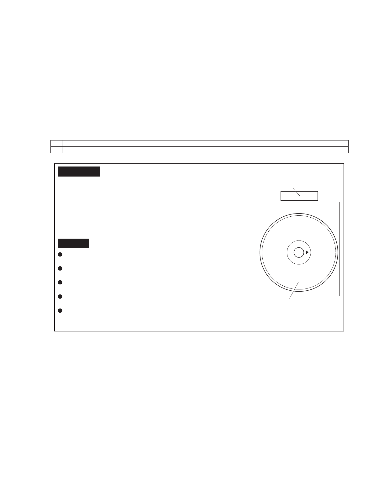
PRECAUTIONS FOR USING LEAD-FREE SOLDER
CHAPTER 1. GENERAL DESCRIPTION
[1] Important Service Safety Precaution ................. 1-1
[2] Important Service Notes (for U.S.A only)..... 1-1
[3] Specifications .................................................... 1-2
[4] Name Of Parts ................................................... 1-3
CHAPTER 2. ADJUSTMENTS
[1] CD Section .................................................. 2-1
[2] Test Mode .................................................... 2-1
[3] Standard Specification Of Stereo System
Error Message Display Contents SYSTEM
PROTECT detection and AMP PROTECT
detection display ......................................... 2-1
CHAPTER 3. MECHANICAL DESCRIPTION
[1] Disassembly ................................................ 3-1
CHAPTER 4. CIRCUIT DESCRIPTION
[1] Waveform Of Servo Circuit .......................... 4-1
[2] Voltage ......................................................... 4-2
CHAPTER 5. FLOWCHART
[1] Troubleshooting ........................................... 5-1
CHAPTER 6. MAJOR PART DRAWING
[1] Function Table of IC ..................................... 6-1
[2] LCD Display................................................. 6-5
CHAPTER 7. DIAGRAMS
[1] Main Block Diagram..................................... 7-1
CHAPTER 8. CIRCUIT SCHEMATICS AND PARTS
LAYOUT
[1] Notes On Schematic Diagram ..................... 8-1
[2] Type Of Transistor And LED ........................ 8-1
[3] Schematic Diagram ..................................... 8-2
[4] Chart Of Connecting Wires.......................... 8-7
[5] Wiring Side Of PWB .................................... 8-8
PARTS GUIDE
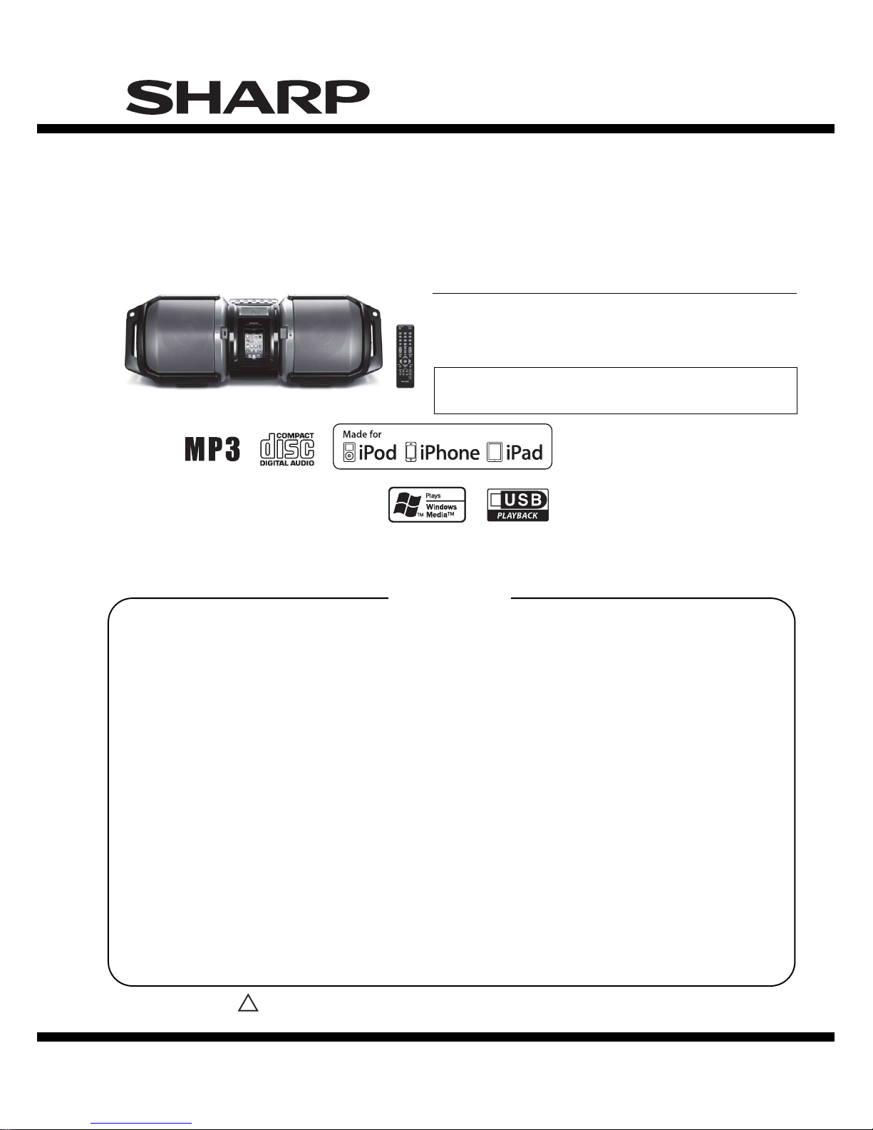
SERVICE MANUAL
No. SX243GXM10UC/
CONTENTS
PORTABLE CD STEREO SYSTEM
MODEL
SHARP CORPORATION
Parts marked with " " are important for maintaining the safety of the set. Be sure to replace these parts with
specified ones for maintaining the safety and performance of the set.
!
• In the interests of user-safety (Required by safety regulations in some
countries) the set should be restored to its original condition and only
parts identical to those specified be used.
GX-M10 (OR
)
[For U.S.A./Canada]
without suffix : GUN METAL COLOR
(OR) : ORANGE COLOR
(RD) : RED COLOR
GX-M10 (RD
)
GX-M10
Page 2
GX-M10
– 2
PRECAUTIONS FOR USING LEAD-FREE SOLDER
1. Employing lead-free solder
Example:
Indicates lead-free solder of tin, silver and copper.
Lead-free wire solder for servicing
2.
Using lead-free wire solder
When fixing the PWB soldered with the lead-free solder, apply lead-free wire solder. Repairing with conventional
lead wire solder may cause damage or accident due to cracks.
As the melting point of lead-free solder (Sn-Ag-Cu) is higher than the lead wire solder by 40°C, we recommend
you to use a dedicated soldering bit, if you are not familiar with how to obtain lead-free wire solder or soldering
bit, contact our service station or s
ervice branch in your area.
3.
Soldering
As the melting point of lead-free solder (Sn-Ag-Cu) is about 220°C which is higher than the conventional lead
solder by 40°C, and as it has poor solder wet ability, you may be apt to keep the soldering bit in contact with the
PWB for extended period of time. However, since the land may be peeled of for the maximum heat-resistance
temperat ure of parts may be exceeded, remove the bit from the PWB as soon as you confirm the steady
soldering condition.
Lead-free solder contains more tin, and the end of the soldering bit may be easily corrected. Make sure to turn
on and off the power of the bit as required.
If a different type of solder stays on the tip of the soldering bit, it is alloyed with lead-free solder. Clean the bit
after every use of it.
When the tip of the soldering bit is blackened during use, file it with steel wool or fine sand paper.
Be careful when replacing parts with polarity indic
ation on the PWB silk.
"MAIN, iPod, DOOR SWITCH, SMPS, DISPLAY, KEY, USB, TRANSIT, SUBW OOFER FLASH (R-CH),
SUBWOOFER FLASH (L-CH), BATTERY TERMINAL 1, BATTERY TERMINAL 2, AC INLET PWB" of this
model employs lead-free solder. The LF symbol indicates lead-free solder, and is attached on the PWB and
service manuals. The alphabetical character following LF shows the type of lead-free solder.
DescriptionParts No.Ref. No.
PWB-A 92LPWB8678MANS MAIN(A1), iPod (A2), DOOR SWITCH (A3)
PWB-B RUiTZA056AWZZ SMPS
DISPLAY (C1) / KEY (C2) / USB (C3) / TRANSIT (C4) /
SUBWOOFER FLASH (L-CH) (C5) / SUBWOOFER FLASH (R-CH) (C6) /
BATTERY TERMINAL 1 (C7) / BATTERY TERMINAL 2 (C8) / AC INLET (C9)
[ For ORANGE Version and GUN METAL Version ]
92LPWB8678DPLSPWB-C
DISPLAY (C1) / KEY (C2) / USB (C3) / TRANSIT (C4) /
SUBWOOFER FLASH (L-CH) (C5) / SUBWOOFER FLASH (R-CH) (C6) /
BATTERY TERMINAL 1 (C7) / BATTERY TERMINAL 2 (C8) / AC INLET (C9)
[ For RED Version ]
PWB-C
92LPWB8761DPLS
i
Page 3
GX-M10
1 – 3
CHAPTER 1. GENERAL DESCRIPTION
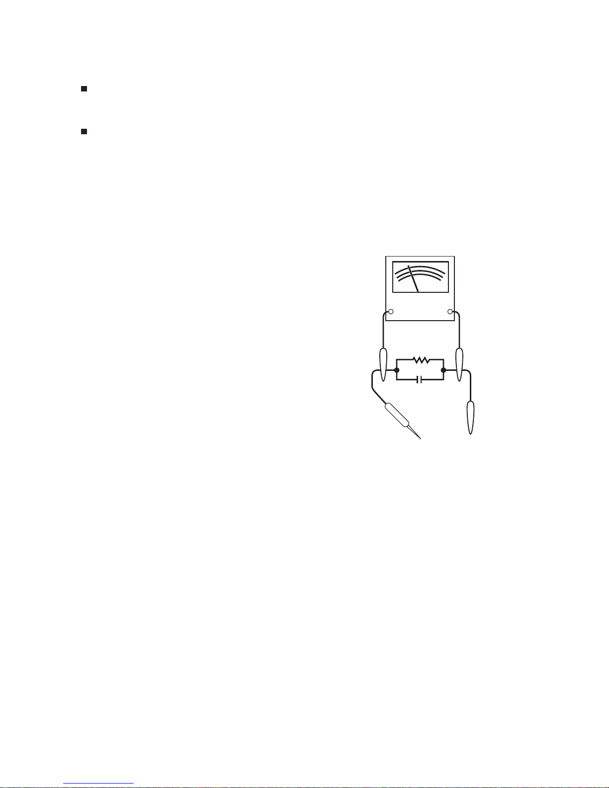
Before returning the audio product to the user, perform
the following safety checks.
2. Inspect all protective devices such as insulating
materials, cabinet, terminal board, adjustment and
compartment covers or shields, mechanical insulators
etc.
3. To be sure that no shock hazard exists, check for
leakage current in the following manner.
*
Plug the AC line cord directly into a
120 volt AC outlet.
*Using two clip leads, connect a 1.5k ohm, 10 watt
resistor paralleled by a 0.15µF capacitor in series
with all exposed metal cabinet parts and a known
earth ground, such as conduit or electrical ground
connected to earth ground.
*
Use a VTVM or VOM with 1000 ohm per volt, or
higher, sensitivity to measure the AC voltage drop
across the resistor (See diagram).
* Connect the resi
stor connection to all exposed metal
parts having a return path to the chassis (antenna,
metal cabinet, screw heads, knobs and control shafts,
escutcheon, etc.) and measure the AC voltage drop
across the resistor.
All check must be repeated
with the AC line cord plug
connection reversed.
Any reading of 0.3 volt RMS (this corresponds to 0.2
milliamp. AC.) Or more is excessive
and indicates a
potential shock hazard which must be corrected before
returning the audio product to the owner.
[2] Important Service Notes (for U.S.A only)
BEFORE RETURNING THE AUDIO PRODUCT
(Fire & Shock Hazard)
[1] Important Service Safety Precaution
CAUTION : “These servicing instructions are for use by qualified service personnel only. To reduce
the risk of electric shock do not perform any servicing other than that contained in the operating
instructions unless you are qualified to do so”.
WARNING
1. For continued safety, no modification of any circuit should be
attempted.
2. Disconnect AC power before servicing.
TO EXPOSED
METAL PARTS
CONNECT TO
KNOWN EARTH
GROUND
0.15 µ F
TEST PROBE
1.5k ohms
10W
VTVM
AC SCALE
1. Inspect all lead dress to make certain that leads are
not pinched or that hardware is not lodged between
the chassis and other metal parts in the audio product
.
1 – 1
Page 4

GX-M10
1 – 4
[3]
Specifications
General
Amplifier
CD player
USB (MP3 / WMA)
Tuner
Speaker
Power source
AC 120 V ~ 60 Hz
15 V (UM/SUM-1, R20) x 10
DC IN 12 V
Power
consumption
AC: Power on: 30 W
DC 12 V: 4.5 A
Dimensions
Width: 30 - 5/16’’ (750 mm)
Height: 10 - 13/16” (275 mm)
Depth: 11 - 1/16” (280 mm)
Weight
(without
batteries and
accessories)
16.8 lbs. (7.6 kg)
Weight
(with batteries)
Approximately 20.2 lbs (9.2 kg)
Output power Front speaker:
RMS: Total 34 watt (17 W per channel
into 3 ohms at 1 kHz, 10% T.H.D.)
FTC: 12.5 watt minimum RMS per
channel into 3 ohms from 200 Hz to
20 kHz, 10% T.H.D.
Subwoofer:
RMS: Total 66 watt into 3 ohms
at 100 Hz, 10% T.H.D.
FTC: 50 watt minimum RMS into
3 ohms from 70 Hz to 200 Hz, 10%
T.H.D.
Output terminals Video output: 1 Vp-p
Headphones: 16 Ω - 50 Ω
(recommended: 32 Ω )
Input terminals Audio In (audio signal):
500 mV/47 k ohms
Mic Input: 200 Ω - 2 kΩ Ø 1/4” (6.3
mm)
Guitar: 100 kΩ - 1 MΩ Ø 1/4” (6.3 mm)
Type Single disc multi-play compact disc
player
Signal readout Non-contact, 3-beam
semiconductor laser pickup
D/A converter Multi bit D/A converter
Frequency
response
20 - 20,000 Hz
Dynamic range 90 dB (1 kHz)
USB host interface
Complies with USB 1.1 (Full
Speed)/2.0 Mass Storage Class.
Support Bulk only and CBI protocol.
Support file
MPEG 1 Layer 3
WMA (Non DRM)
Bitrate support
MP3 (32 ~ 320 kbps)
WMA (64 ~ 160 kbps)
Other
Maximum total number of MP3/WMA
files is 65025.
Maximum total number of folders is
999 INCLUSIVE of root directory.
The ID3TAG information supported
are TITLE, ARTIST and ALBUM only.
Supports ID3TAG version 1 and
version 2.
File system
support
Support USB devices with
Microsoft Windows/DOS/FAT 16/
FAT 32.
2 kbyte block length for sector.
Frequency range FM: 87.5 - 108 MHz
Preset 40 (FM station)
Type
2-way type speaker system
Front Speakers:
3-1/8” (8 cm) - 3 Ω - Full Range
Subwoofer: 5- 1/8” (13 cm) - 6 Ω
- Woofer (light-up)
Maximum input
power
Front Speakers: 34W / Channel
Subwoofer: 66W / Channel
Rated input power
Front Speakers: 17W / Channel
Subwoofer: 33W / Channel
1 – 2
Page 5
GX-M10
1 – 5
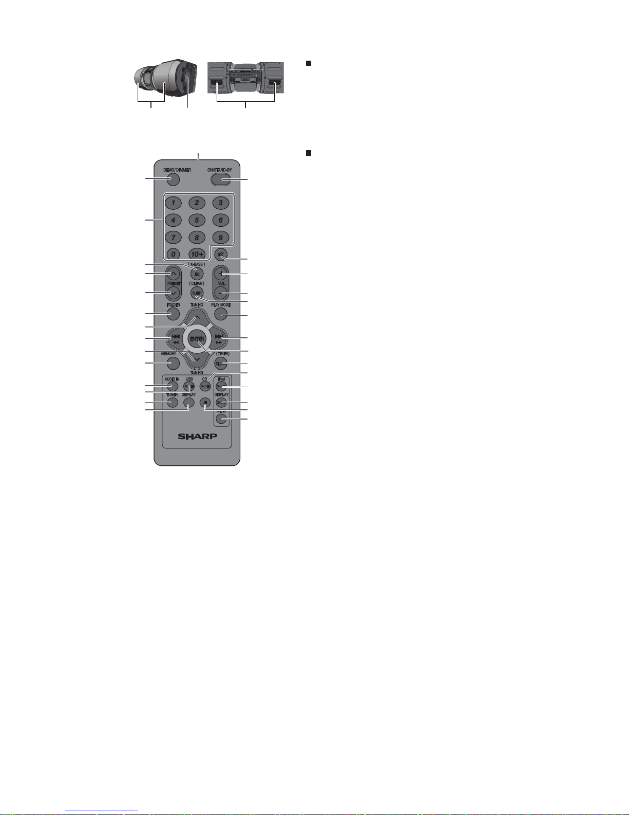
[4] Names Of Parts
1. Equaliser/X-Bass Button
2. Power On/Stand-by Button
3. Demo/Dimmer/Stop Button
4. Tuner/Audio In Button
5. Tuner Preset Down, CD/USB Track Down,
iPod/iPhone Skip Down
6. USB Play/Pause Button
7. Tuner Preset Up, CD/USB Track Up,
iPod/iPhone Skip Up
8. CD Play/Pause Button
9. Volume Down Button
10. iPod Play/Pause Button
11. Volume Up Button
12. Docking station door open knob
13. Timer indicator
14. Remote sensor
15. Docking station
16. USB/iPad Terminal
17. CD compartment
18. CD compartment open knob
Front Panel
1. FM antenna
2. DC 12 V input jack
3. Headphone jack
4. Microphone volume knob
5. Microphone input jack
6. Guitar input jack
7. Guitar volume knob
8. Audio input jack
9. Video output jack
10. AC input jack
11. Cable holder
Rear panel
1. CD Indicator
2. USB Indicator
3. MP3 Indicator
4. WMA Indicator
5. iPod Indicator
6. FM Stereo Mode Indicator
7. Stereo Station Indicator
8. Total Indicator
9. Folder Indicator
10. Title Indicator
11. MEM (Memory) Indicator
12. X-bass Indicator
13. Sleep Indicator
14. Once Timer Indicator
15. Daily Timer Indicator
16. RDM (Random) Indicator
17. Repeat Indicator
18. Microphone Indicator
19. Guitar Indicator
20. Battery Level Indicator
21. Play Indicator
22. Pause Indicator
Display
X-BASS/EQ
DEMO/DIMMER
VOLUME
iPod
CD
USB
TUNER/AUDIO-IN
ON/STAND-BY
PORTABLE MUSIC BOOMBOX GX-M10
PRESET
R
E
M
I
T
T
OME
R
E
R
O
S
N
E
S
11 3 579 11
2468 10
13
12
14
16
15
17
18
1 2 3 4 5 6 7
201918171615141312111098
21
22
1 2 3 4 5 6 7 8 9
10
11
1 – 3
Page 6
GX-M10
1 – 6
1. Remote Control Transmitter
2. Demo/Dimmer Button
3. Numeric Buttons
4. Equalizer (X-Bass) Button
5. Tuner Preset Up Button
6. Tuner Preset Down Button
7. Folder Button
8. Tuning Up, iPod Cursor Up, Folder Up Button
9. Skip Down, Fast Reverse, Time Down Button
10. Tuning Down, iPod Cursor Down,
Folder Down Button
11. Memory Button
12. Audio In Button
13. USB Play/Pause Button
14. Tuner Button
15. Display Button
16. On/Stand-by Button
17. Mute Button
18. Volume Up Button
19. Volume Down Button
20. Sleep (Clear) Button
21. Play Mode/Random Button
22. Skip Up, Fast Forward, Time Up Button
23. Enter Button
24. Clock (Timer) Button
25. CD Play/Pause Button
26. iPod Play/Pause Button
27. iPod Display (TV OUT) Button
28. CD/USB Stop Button
29. iPod Menu Button
Remote Control
1. Front speaker
2. Subwoofer
3. Bass Reflex Duct
Speakers
T
R
O
P
AB
L
E
MU
I
S
CXO
B
MO
O
B G
X
-
M
1
0
3
21
7
8
10
13
12
11
15
14
5
2
4
6
3
9
16
17
18
19
20
21
22
23
24
25
27
29
28
26
1
1 – 4
Page 7
GX-M10
2 – 1
CHAPTER 2. ADJUSTMENTS
[1] CD Section
• Adjustment
Since this CD system incorporates the following
automatic adjustment functions, readjustment is not
needed when replacing the pickup. Therefore,
different PWBs and pickups can be combined freely.
Each time a disc is changed, these adjustments are
performed automatically. Therefore, playback of
each disc can be performed under optimum
conditions.
Items adjusted automatically
1) Offset adjustment (The offset voltage between the
head amplifier output and the VREF reference
voltage is compensated inside the IC)
* Focus offset adjustment
* Tracking offset adjustment
2) Tracking balance adjustment
3) Gain adjustment (The gain is compensated inside
the IC so that the loop gain at the gain crossover
frequency will be 0 dB.)
* Focus gain adjustment
* Tracking gain adjustment
[2] Test Mode
[Test Mode Input Method]
1. During power stand-by DEMO ON condition, press [1] -> [2] -> [4] -> [5] buttons at remote control sequently.
5. [Exiting Test Mode]
5.1. While in Version display or in Test Mode Function press ON / STAND-BY button (main unit).
5.2.
2. MCU will start up with software version display as below.
" GX# ymdd$ "
Press EQ/X-BASS Key at Main unit
y : year ( in Hexa code. Eg: 2012 C )
m : month ( in Hexa code. Eg: 07 7, 10 A )
dd : day (Eg: 01)
$ : A, B, C, ...... Z
RR : version (00 ~ 99)
# : area setting H : Europe
U : USA
Vxxxx : Servo F/W version
" GX#_10RR "
Press EQ/X-BASS Key at Main unit
Press EQ/X-BASS Key
at Main unit
" 618Vxxxx "
3. Press [OPEN / CLOSE] button at the main unit to enter the KEY Test Mode.
4. The display will change as below for each main unit button is pressed.
[TUNER / AUDIO IN] : Display "KEY 2-1"
[PRESET DOWN] : Display "KEY 6-3"
[PRESET UP] : Display "KEY 6-4"
[USB PLAY / PAUSE] : Display "KEY 3-1"
[VOL UP] : Display "KEY 6-6"
[STOP] : Display "KEY 6-1"
[CD PLAY / PAUSE] : Display "KEY 4-1"
[VOLUME DOWN] : Display "KEY 6-5"
[iPod PLAY / PAUSE] : Displa
y "KEY 5-1"
[EQ / X-BASS] : Display "KEY 6-2"
All display light up in Backlight On (2sec) => Backlight Off (2sec) => finally display "RESET" and execute reset,
before go to standby (demo).
[3] Standard Specification Of Stereo System Error Message Display Contents
SYSTEM PROTECT detection and AMP PROTECT detection display
Example: In case of speaker abnormal
1: SYSTEM PROTECT
2 : AMP Over Temperature Warning Protect
3 :AMP Shut Down Protect
4 : FAULT
OFF
FLASHING
ON
No.1
1 Frame
(Repeat)
OFFOFF
( 3 Sec )
No.2
No.3 No.4
No.1
No.2
( 3 Sec )
( 3 Sec )
( 3 Sec )
OFF
ON
ON
OFF
FLASHING
ON
OFF
)ceS3 () ceS3 (
( 3 Sec )
In case AMP Shut Down, SYSTEM PROTECT, FAULT PROTECT or AMP Over-Temp Warning Protect has occurred,
the unit will automatically enter to stand-by mode ON/Standby LED willl be flashing as below:-
Page 8
GX-M10
3 – 1
CD-ES700/CD-ES77CD-ES700/CD-ES77Service ManualCD-ES700/CD-ES77MarketE
CHAPTER 3. MECHANISM DESCRIPTION
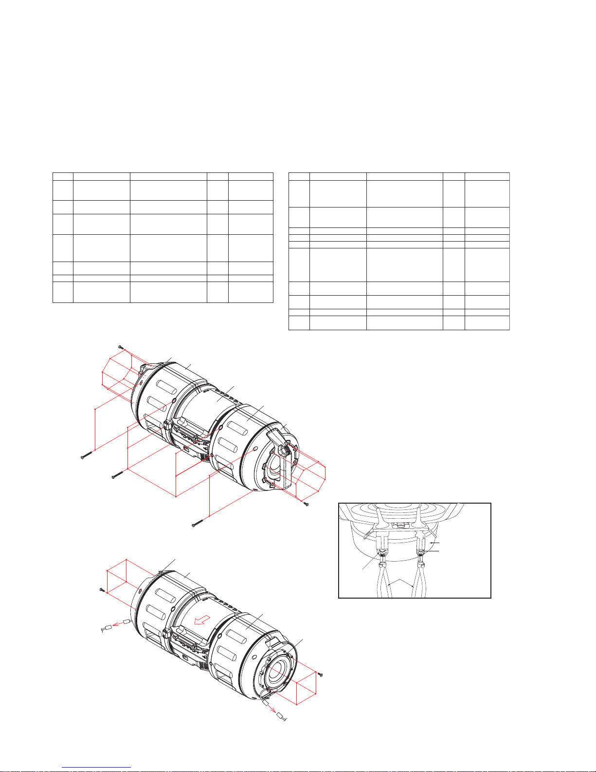
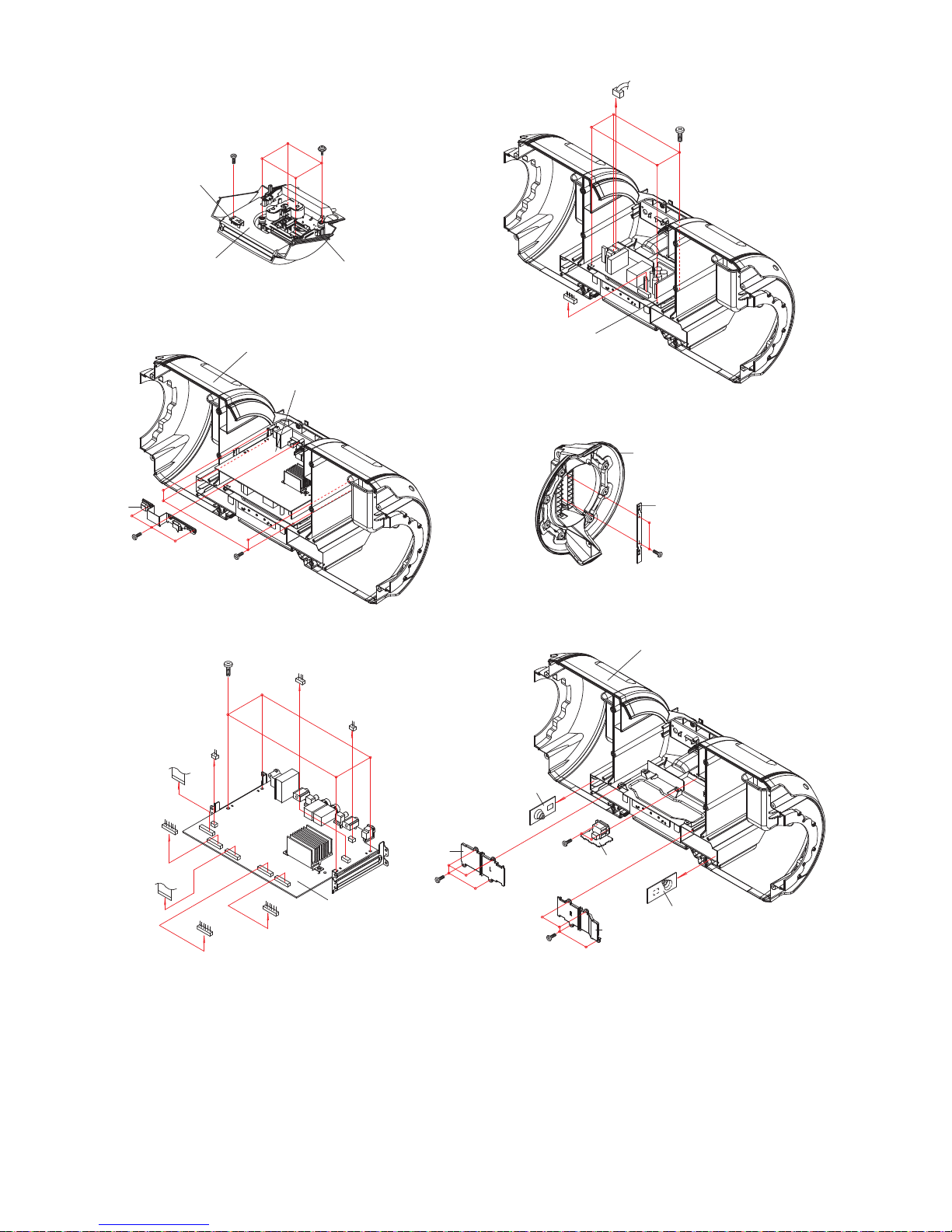
[1] Disassembly
Caution On Disassembly
Follow the below-mentioned notes when disassembling the unit and reassembling it, to keep it safe and ensure
excellent performance:
1. Take compact disc out of the unit.
2. Be sure to remove the power supply plug from the wall outlet before starting to disassemble the unit.
3. Take off nylon bands or wire holders where they need to be removed when disassembling the unit. After servicing
the unit, be sure to rearrange the leads where they were before disassembling.
4. Take sufficient care on static electricity of integrated circuits and other circuits when servicing.
(A1) x 8
M4 x 14mm
(B1) x 4
M3.5 x 10mm
(B1) x 4
M3.5 x 10mm
(A2) x 2
M3 x 30mm
(C1) x 6
M3 x 30mm
(A2) x 2
M3 x 30mm
(A1) x 8
M4 x 14mm
Figure 2
Figure 1
Front Cabinet Ass’y
(A3) x 1
From Side Cabinet Ass’y
(A3) x 1
From Side Cabinet Ass’y
Side Cabinet Ass’y (Left)
Side Cabinet Ass’y (Right)
Subwoofer (Right)
Subwoofer (Left)
Back Cabinet Ass’y
Back Cabinet Ass’y
Top Cabinet Ass’y
Front Cabinet Ass’y
CAUTION:
TO REMOVE SPEAKER UNIT, PRESS THESE LOCKING TABS
TO RELEASE SPEAKER WIRES.
SPEAKER UNIT
LOCKING
TA B
LOCKING TAB
SPEAKER
WIRE
STEP REMOVAL PROCEDURE FIGURE STEP REMOVAL PROCEDURE FIGURE
1 Side Cabinet Ass'y (A1)x16 1 8 Speaker (H1)x2 3
(Left/Right) (A2)x4 1 (Left/Right) (H2)x8 3
(A3)x2 2 (H3)x8 5
2Subwoofer (B1)x8 2 (H4)x4 5
(Left/Right) (B2)x4 9 iPod PWB ( J1)x1 6
3 Back Cabinet Ass'y (C1)x6 1 (J2)x1 6
(C2)x9 3,5,11,12 (J3)x2 7
(C3)x2 11 10 Top Cabinet Ass'y (K1)x2 8
4Display PWB (D1)x1 3 11 CD Mechanism Unit (L1)x4 9
(D2)x6 3 12 Door Switch PWB (M1)x1 9
(D3)x2 4 13 Main PWB (N1)x1 8
(D4)x1 4 (N2)x2 8
5 Key PW B (E1)x1 4 (N3)x1 10
(E2)x3 (N4)x7 10
6 USB PWB (F1)x1 3 (N5)x4 11
7Transit PWB (G1)x1 5 14 SMPS PWB (P1)x4 12
(G2)x3 (P2)x1
(G3)x1 15 Subwoofer Flash(Q1)x413
PWB (R-CH / L-CH )
16 AC Inlet PWB (R1)x2 14
17
Battery Terminal 1
(S1)x2 14
and 2 PWB
(S2)x8
1. Speaker Cup .....................
2. Screw.................................
3. Screw.................................
4. Terminal ............................
1. iPod Door...........................
2. iPod Holder Ass'y ..............
3. Screw.................................
1. Screw.................................
1. Screw.................................
1. Screw.................................
1. Screw.................................
2. Mic Knob............................
3. Bracket ..............................
4. Screw.................................
5. Screw.................................
1. Screw.................................
2. Socket ...............................
1. Screw.................................
1. Screw.................................
1. Battery Cover.....................
2. Screw.................................
1. Screw.................................
2. Screw.................................
3. Socket ...............................
1. Screw.................................
2. Terminal ............................
1. Screw.................................
2. Socket ...............................
3. Flat Cable ..........................
1. PWB Holder Ass'y .............
2. Screw.................................
3. Screw.................................
4. Flat Cable ..........................
1. Function Button .................
2. Screw.................................
1. Screw.................................
1. iPod Cover.........................
2. Screw.................................
3. Socket ...............................
Page 9
GX-M10
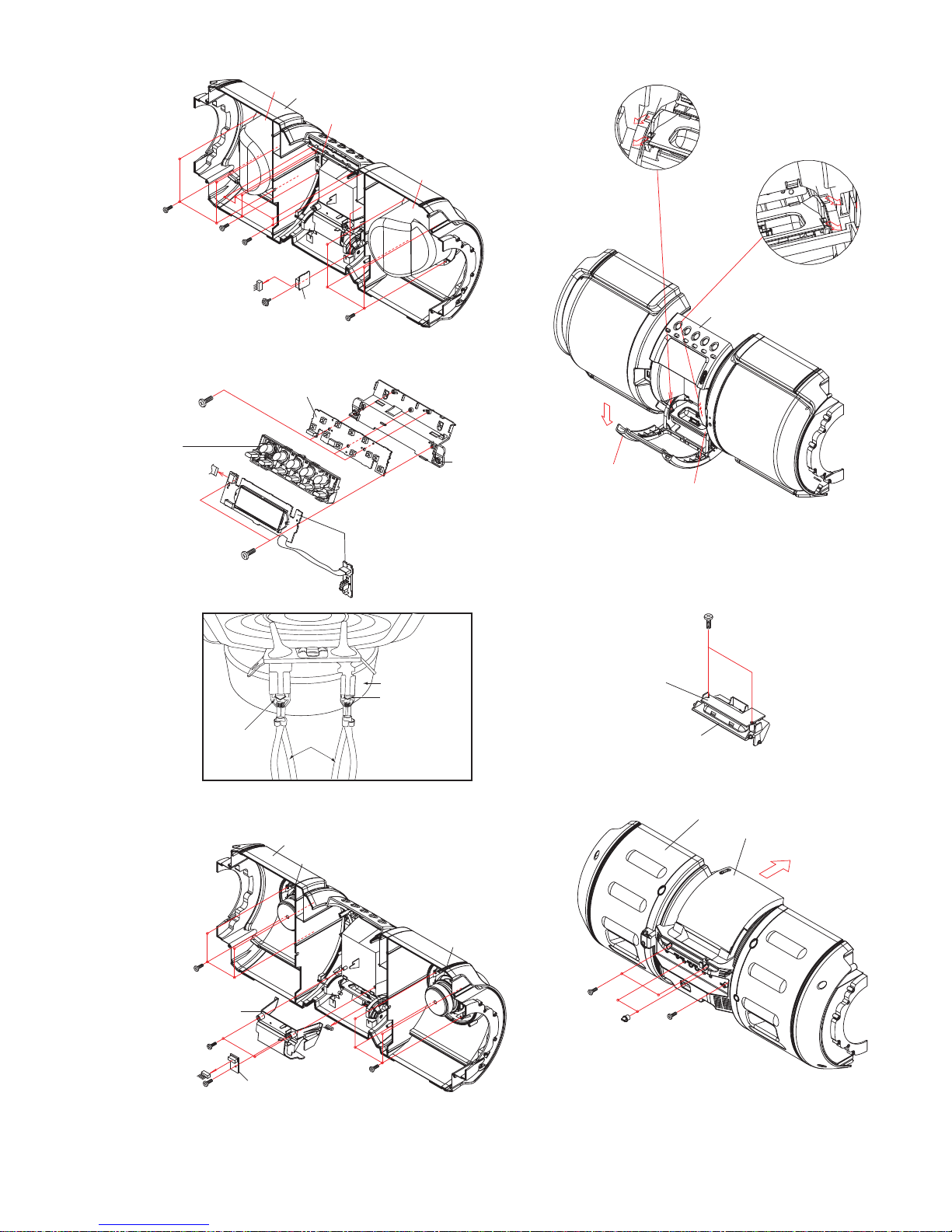
3 – 2
(H2) x 4
M3 x 10mm
(H2) x 4
M3 x 10mm
(D2) x 2
M3 x 10mm
(D2) x 4
M3 x 10mm
USB PWB
Key PWB
PWB Holder
Display PWB
(F1) x 1
Special Screw
(C2) x 1
From Main PWB
(E2) x 3
M2.6 x 8mm
(J3) x 2
M3 x 8mm
iPod PWB
iPod Holder Ass’y
(D3) x 2
M2.6 x 8mm
(H3) x 4
M3.5 x 10mm
(H3) x 4
M3.5 x 10mm
(N1) x 1
M3 x 10mm
(K1) x 2
M3 x 10mm
(N2) x 2
Mic Knob
(G3) x 1
From
Transit
PWB
(G2) x 2
M3 x 8mm
(C2) x 1
From Main PWB
(G2) x 1
M3 x 8mm
Tr ansit PWB
iPod Cover
(G1) x 1
(D4) x 1
Function Knob
(E1) x 1
(J1) x 1
iPod Door
(H1) x 1
Speaker Cup
(H1) x 1
Speaker Cup
Figure 6
Figure 7
Figure 5
Figure 8
Figure 3
Figure 4
Front Cabinet Ass’y
Front Cabinet Ass’y
Front Cabinet Ass’y
Back Cabinet Ass’y
Top Cabinet Ass’y
Speaker (Right)
Speaker (Left)
(J2) x 1
iPod Holder Ass’y
(D1) x 1
PWB Holder Ass’y
OPEN
CAUTION:
TO REMOVE SPEAKER UNIT, PRESS THESE LOCKING TABS
TO RELEASE SPEAKER WIRES.
SPEAKER UNIT
LOCKING
TA B
LOCKING TAB
SPEAKER
WIRE
Page 10
GX-M10
3 – 3
(M1) x 1
M3 x 8mm
Door Switch PWB
Top Cabinet Ass’y
Back Cabinet Ass’y
Subwoofer Flash PWB
(L-CH / R-CH)
Side Cabinet Ass’y (Left / Right)
Back Cabinet Ass’y
Main PWB
SMPS PWB
(N4) x 4
M3 x 10mm
(P1) x 4
M3 x 8mm
(Q1) x 2
M3 x 6mm
(N4) x 3
M3 x 10mm
(N5) x 4
M3 x 8mm
(S2) x 4
M3 x 10mm
(S2) x 4
M3 x 10mm
(R1) x 2
M3 x 10mm
(C2) x 1
From Battery Terminal 1
(C2) x 1
From Main PWB
(P2) x 1
From AC Inlet PWB
(C2) x 1
From AC Inlet PWB
Main PWB
Battery Terminal 2 PWB
Battery Terminal 1 PWB
AC Inlet PWB
Battery Cover
(S1) x 1
Battery Cover
(S1) x 1
(C2) x 1
From Door Switch PWB
(C3) x 1
From Display PWB
(C2) x 1
From CD Motor PWB
(C3) x 1
From CD Pickup Unit
(C2) x 1
From Subwoofer Flash (R-CH)
(C2) x 1
From Subwoofer Flash (L-CH)
(N3) x 1
Bracket
CD Mechanism Unit
(L1) x 4
Special Screw
Figure 9
Figure 12
Figure 13
Figure 14
Figure 10
Figure 11
Page 11
GX-M10
4 – 1
CHAPTER 4. CIRCUIT DESCRIPTION
[1] Waveform Of Servo Circuit
48
IC1
1
FOP
49
IC1
2
TRP
Figure 1
48
IC1
1
FOP
138
IC1
4
TE
67
IC1
7
RFOUT
Figure 2
138
IC1
4
RFOUT
67
IC1
7
TE
Figure 3
Figure 5
Figure 4
48
IC1
4
FOP
50
IC1
3
SPOUT
Page 12
GX-M10
4 – 2
[2] Voltage
Pin
No.
Voltage ( V)
Pin
No.
Voltage ( V)
Pin
No.
Voltage ( V)
Pin
No.
Voltage ( V)
1 1.78 17 1.85 33 1.82 49 1.62
2 0.07180.02340.01501.62
3 0.73 19 0.76 35 0.01 51 1.62
4 0.92200.88363.17521.62
5 0.05 21 0.01 37 0.00 53 0.01
6 0.05220.01380.01540.00
7 0.02 23 0.01 39 3.24 55 0.03
8 0.05 24 3.29 40 0.16 56 0.03
9 3.43253.06411.62570.03
10 1.25 26 1.66 42 0.16 58 0. 03
11 3.06 27 -0.02 43 1. 62 59 3.65
12 3.17 28 -0.02 44 0. 16 60 3.65
13 3.06 29 0.01 45 0.16 61 3. 65
14 3.06 30 0.00 46 0.16 62 3. 64
15 3.20 31 1.23 47 0.16 63 1. 59
16 0.00 32 0.05 48 1.88 64 0. 05
IC500
Pin
No.
Voltage ( V)
Pin
No.
Voltage ( V)
Pin
No.
Voltage ( V)
Pin
No.
Voltage ( V)
1 12.03 12 3.22 23 12.04 34 21.90
2 3.17 13 3.22 24 21. 90 35 21.54
3 0.00 14 0.00 25 2.80 36 10.64
4 0.00 15 0.00 26 21. 53 37 0.00
5 3.17 16 1.62 27 21. 53 38 0.00
6 1.62173.24281.063910.60
7 3.24 18 1.62 29 0.00 40 22.07
8 1.62 19 0.00 30 0.00 41 22.07
9 1.18 20 0.00 31 10. 58 42 0.00
10 0.00 21 12.08 32 21. 88 43 22.05
11 0.00 22 12.04 33 21. 86 44 12.09
IC900
Pin
No.
Voltage (V)
Pin
No.
Voltage (V)
Pin
No.
Voltage ( V)
Pin
No.
Voltage ( V)
1 1.65 12 1.65 23 1.64 34 1.65
2 1.65131.65241.64351.65
3 1.65 141.65 251.64361.65
4 1.65 151.65 261.64371.65
5 1.65 161.65 271.64383.29
6 1.65 17 -0. 01 28 1.64 39 0.00
7 1.65 18 -0. 01 29 1.64 40 3.29
8 1.65191.64301.65413.29
9 1.65 201.64 311.65420.71
10 1.65 21 1.64 32 1.65 43 2. 95
11 1.62 22 1.64 33 1.65 44 2. 75
IC701
Pin
No.
Voltage (V)
Pin
No.
Voltage ( V)
Pin
No.
Voltage ( V)
Pin
No.
Voltage (V)
1 3.15 17 2.92 33 3.05 49 3.17
2 3.30180.72343.33503.17
3 3.04 19 2.88 35 2.95 51 3.17
4 0.95203.16363.17523.17
5 0.74213.16373.06533.17
6 3.03223.08380.12543.17
7 1.56233.06393.30553.01
8 0.02240.01403.00562.74
9 0.02253.06413.06571.75
10 3.06 26 3.08 42 3.18 58 0. 00
11 3.05 27 2.20 43 3.18 59 0. 00
12 3.06 28 2.75 44 2.88 60 3. 15
13 3.06 29 3.16 45 2.89 61 3. 17
14 3.06 30 3.30 46 2.89 62 3. 06
15 3.06 31 0.02 47 3.07 63 1. 80
16 0.50 32 0.17 48 2.83 64 3. 06
IC600
Pin
No.
Voltage ( V)
10.17
20.17
30.00
40.00
50.00
60.20
70.08
86.00
IC401
Pin
No.
Voltage ( V)
10.02
20.02
30.00
40.00
50.00
60.04
70.03
80.00
IC431
Pin
No.
Voltage ( V)
16.81
26.11
36.08
40.00
51.62
68.38
7 10.75
86.00
IC451
Pin
No.
Voltage ( V)
16.92
26.06
35.91
40.00
55.91
66.06
76.92
8 11.92
IC461
Pin
No.
Voltage ( V)
14.76
24.11
34.10
40.00
50.00
64.17
74.00
85.90
IC550
Pin
No.
Voltage ( V)
Pin
No.
Voltage ( V)
12.5681.54
20.0091.39
3 5.07 10 0.00
4 3.29 11 0.00
5 0.00 12 0.00
61.45132.53
71.65142.50
IC580
Pin
No.
Voltage (V)
Pin
No.
Voltage ( V)
1 0.13 9 12.06
2 0.00 10 0.00
30.001112.07
4 0.00 12 -0. 10
50.01130.00
60.001412.08
7 0.00 15 0.00
80.001612.08
IC590
Pin
No.
Voltage ( V)
13.25
23.25
3NC
40.00
IC681
Page 13
GX-M10
4 – 3
Pin
No.
Voltage ( V)
10.73
23.31
30.00
43.78
51.18
IC801
Pin
No.
Voltage ( V)
19.92
2 21.63
35.17
4 -0.02
50.79
60.99
73.09
83.58
IC802
Pin
No.
Voltage (V)
14.98
20.09
30.74
40.05
51.25
65.07
75.04
83.35
IC803
Pin
No.
Voltage (V)
19.94
221.53
35.02
4 -0.07
50.80
60.92
73.09
83.59
IC804
Pin
No.
Voltage ( V)
15.05
20.00
35.05
4NC
53.32
IC805
5.05 5.07 4.24 0.00 0.00 1.74 3.16 12.06 0.00
4.24 0.11 2.97 0.68 0.68 0.01 -0.01 0.01 0.74
5.07 4.83 0.00 0.01 0.01 1.79 -0.01 0.00 0.00
B
E
Q552
Voltage ( V)
Q553
Voltage ( V)
Q554
Voltage ( V)
Q591
Voltage ( V)
Q593
Voltage ( V)
C
TRANSISTOR
TERMINAL
Q492
Voltage ( V)
Q493
Voltage ( V)
Q494
Voltage ( V)
Q551
Voltage ( V)
CD / Servo section
Pin
No.
Voltage ( V)
Pin
No.
Voltage ( V)
Pin
No.
Voltage ( V)
Pin
No.
Voltage ( V)
Pin
No.
Voltage ( V)
Pin
No.
Voltage ( V)
Pin
No.
Voltage ( V)
Pin
No.
Voltage ( V)
1 3.33 19 2.80 m 37 1.14 55 1.67 73 1.65 91 3.10 m 109
3.28
127
0.10 m
2 4.10 m 20 3.34 38 1.14 56 1.67 74 0.82 92 3.34 110
3.33
128
3.33
3 4.00 m 21 3.34 39 1.13 57 1.67 75 0.81 93 3.10 m 111
4.90 m
129
0.10 m
4 3.90 m 22 4.30 m 40 1.14 58 1.67 76 422.70 m 94 1.67 112
4.90 m
130
2.80 m
5 3.90 m 23 3.34 41 1.14 59 1.67 77 2.90 m 95 1.67 113
3.33
131
3.33
6 4.00 m 24 4.40 m 42 1.13 60 1.67 78 3.32 96 1.21 114
3.33
132
4.00 m
7 3.34 25 3.34 43 1.14 61 6.10 m 79 3.33 97 3.34 115
0.43
133
4.00 m
81.2
1263.34441.14623.31803.31983.40 m116
1.66
134
3.33
9 2.80 m 27 1.42 45 3.34 63 5.90 m 81 3.70 m 99 3.30 m 117
1.56
135
1.67
10 3.33 28 3.34 46 2.90 m 64 3.32 82 3.70 m 100 3.30 m 118
5.50 m
136
1.09
11 3.32 29 3.34 47 1.20 65 1.65 83 3.70 m 101 1.20 119
1.42
137
344.80 m
12 3.32 30 2.91 48 1.67 66 1.73 84 3.80 m 102 3.30 m 120
3.33
138
1.65
13 4. 00 m 31 2.55 49 1.67 67 1.58 85 3.80 m 103 3.34 121
1.20
139
4.00 m
14 3. 90 m 32 3.34 50 1. 67 68 1.79 86 3.90 m 104 3.23 122
3.30 m
140
4.00 m
15 4. 00 m 3
3 396.50 m 51 1.67 69 1.02 87 1.20 105 3.22 123
0.40 m
141
4.00 m
16 3.33 34 3.26 52 3.90 m 70 1.21 88 3.33 106 3.30 124
3.33
142
4.00 m
17 3.33 35 3.34 53 1.67 71 1.19 89 1.53 107 3. 21 125
3.33
143
4.00 m
18 3.34 36 2. 90 m 54 1.67 72 1.65 90 1.48 108 3.21 126
0.30 m
144
4.00 m
IC1 (MN6627992AB)
Page 14
GX-M10
4 – 4
Pin
No.
Voltage ( V)
Pin
No.
Voltage ( V)
Pin
No.
Voltage ( V)
Pin
No.
Voltage ( V)
Pin
No.
Voltage ( V)
Pin
No.
Voltage ( V)
1 3. 33 10 4.00 m 19 2.90 m 28 2. 70 m 37 3.34 46 2.70 m
2 4.00 m 11 4.00 m 20 4.00 m 29 3. 33 38 1.42 47 4.00 m
3 3.33 122.80 m214.00 m304.10 m39 3.33 484.00 m
4 4.00 m 13 4.00 m 22 3.90 m 31 3. 34 40 433.10 m 49 3. 33
5 4.00 m 14 3.34 23 4.00 m 32 4.20 m 41 2.80 m 50 4.10 m
6 2.80 m 15 3.33 24 3.33 33 4.20 m 42 4.00 m 51 4.10 m
7 4.00 m 16 3.33 25 4.00 m 34 3.34 43 3.34 52 2.80 m
8 4.00 m 17 3.32 26 4.00 m 35 3.33 44 4.10 m 53 4.00 m
9 3. 33 18 3.32 27 3.34 36 435. 60 m 45 4. 10 m 54 2.80 m
IC6(EM638165 S DRAM )
Pin
No.
Voltage ( V)
1 0.40 m
25.26
348.30 m
4 0.50 m
5 319.30 m
63.29
7 378.60 m
84.31
95.26
10 3.29
IC5(TPS2561D)
Pin
No.
Voltage ( V)
13.80 m
23.33
3 385.10 m
4 418.20 m
5 437.10 m
63.33
73.4m
83.33
IC3( MF1337S395)
Pin
No.
Voltage ( V)
12.57
22.90
32.33
42.80 m
53.26
60.41
73.33
83.33
IC7(W25Q16BV)
Pin
No.
Voltage ( V)
10.66
20.30 m
30.30 m
40.30 m
53.00 m
60.40 m
70.40 m
83.21
IC4(TS3USB++ )
Pin
No.
Voltage ( V)
Pin
No.
Voltage ( V)
1 1.66 15 2.62
2 4.38 16 2.64
3 1.86 17 2.62
4 1.66 18 5.08
5 1.25 19 1.95
6 10.90 m 20 5.08
7 11.00 m 21 1.90 m
8 5.08 22 1.90 m
9 3.30 m 23 1. 66
10 3.30 m 24 5.04
11 2.60 25 5.06
12 2.60 26 1.66
13 2.64 27 1.67
14 2.62 28 5.08
IC12 (SA5888)
Page 15
GX-M10
5 – 1
CHAPTER 5. FLOWCHART
[1] Troubleshooting
1. When the CD does not function
The CD section may not operate when the objective lens of the optical pickup is dirty. Clean the objective lens, and
check the playback operation. When this section does not operate even after the above step is taken, check the
following items.
Remove the cabinet and follow the troubleshooting instructions.
"Track skipping and/or no TOC (Table Of Contents) may be caused by build up of dust other foreign
matter on the
laser pickup lens. Before attempting any adjustment make certain that the lens is clean. If not, clean it as mentioned
below."
Turn the power off.
Gently clean the lens with a lens cleaning tissue and a small amount of isopropyl alcohol.
Do not touch the lens with the bare hand.
2. When a CD cannot be played
2.1. Pressing the CD operation key is accepted, but playback does not occur.
1) Focus-HF system check
2) Tracking system check
3) Spin system check
4) PLL system check
Parts code
1. CD optical pickup Lens cleaner disc UDSKA0004AFZZ
HOW TO USE
CAUTION
Cleaning fluid
Cleaner disc
Using the brush in the cleaner cap, apply 1 or 2 drops of the cleaning fluid to the
brush on the CD cleaner disc which has the mark next to it.
Place the CD cleaner disc onto the CD disc tray with the brush side down, then
press the play button.
You will hear music for about 20 seconds and the CD player will automatically stop.
If it still play continuously, press the stop button.
1.
2.
3.
The CD lens cleaner should be effective for 30-50 operations, however if the
brushes become worn out earlier then please replace the cleaner disc.
If the CD cleaner brushes become very wet then wipe off any excess fluid with a soft
cloth.
Do not drink the cleaner fluid or allow it contact with the eyes. In the event of this
happening then drink and / or rinse with clean water and seek medical advice.
The CD cleaner disc must not be used on car CD players or on computer CD-ROM
drives.
All rights reserved. Unauthorized duplicating, broadcasting and renting this product
is prohibited by law.
Page 16
GX-M10
5 – 2
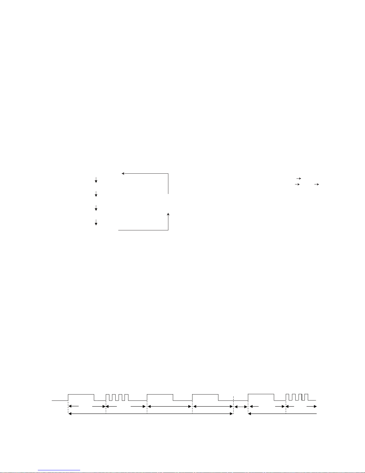
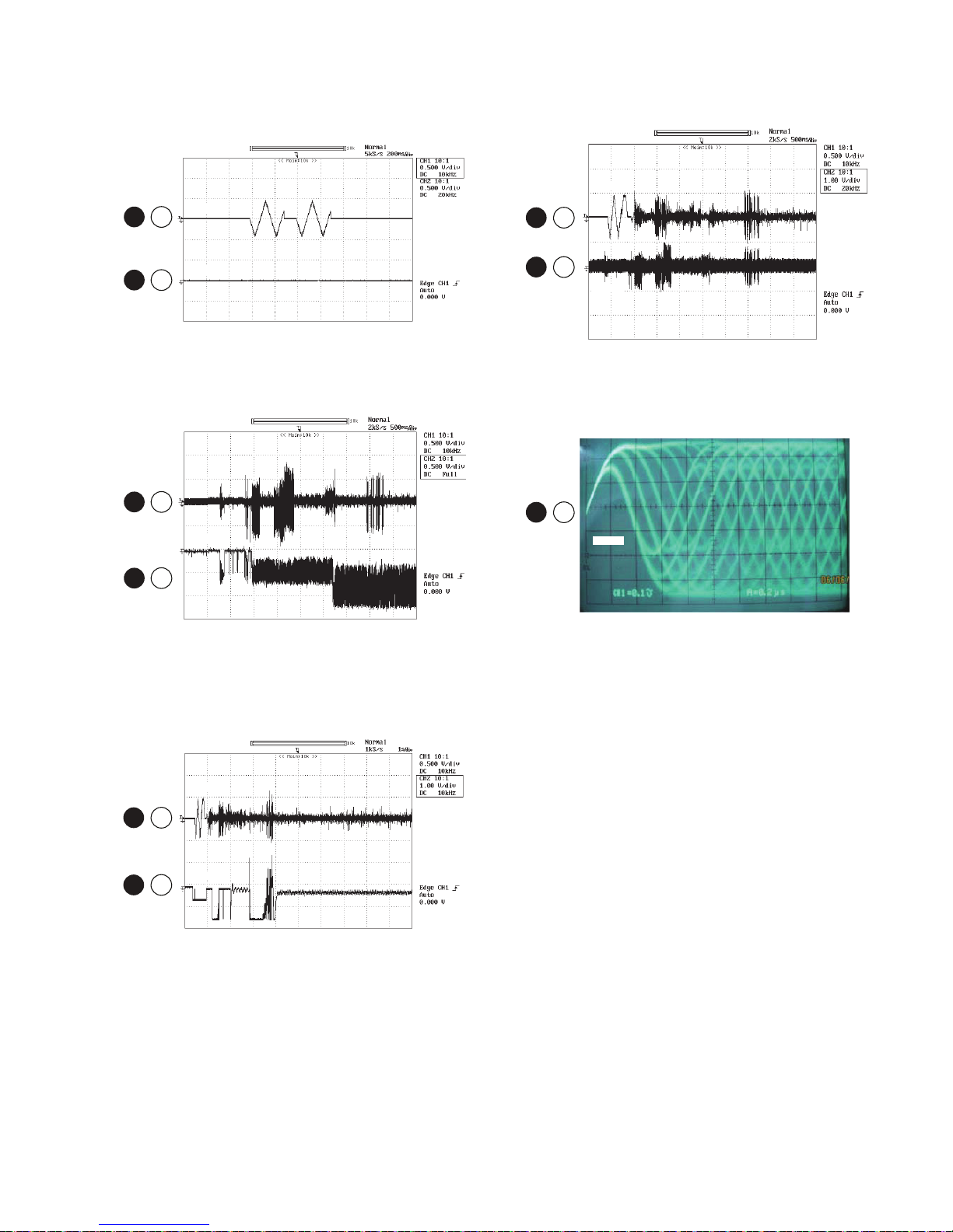
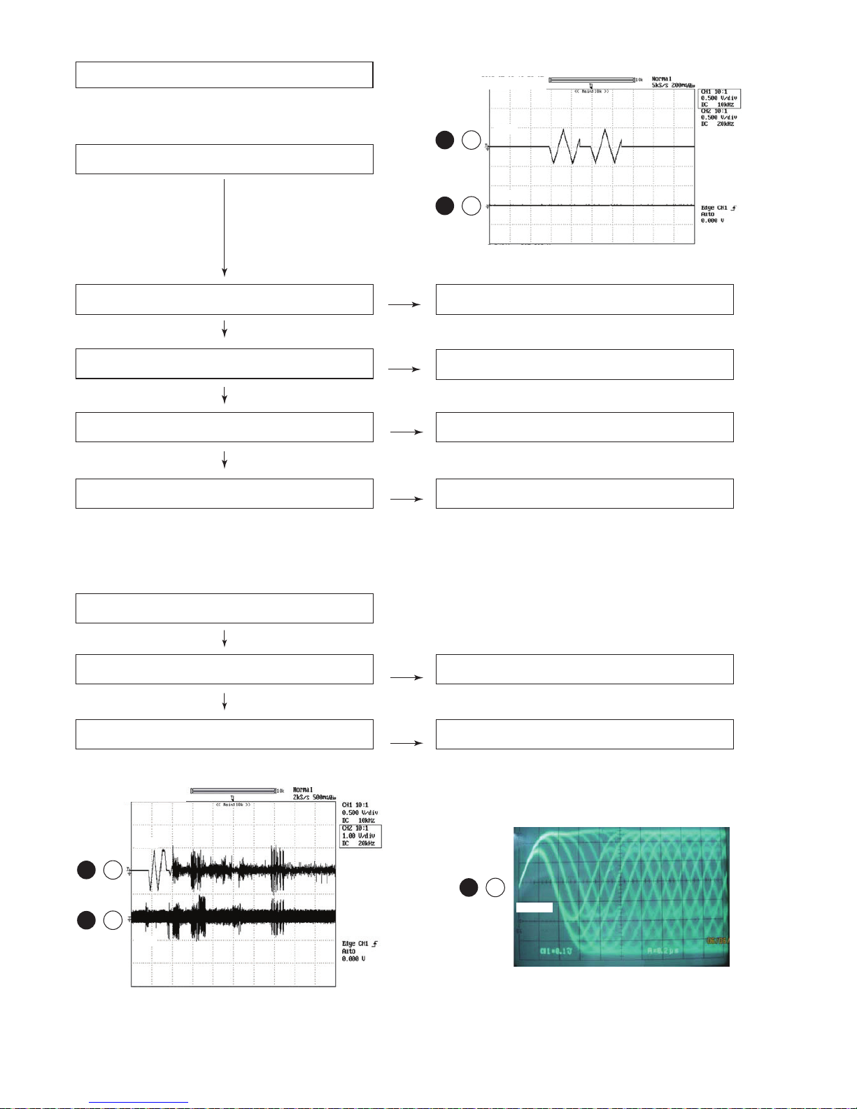
(1) Focus-HF system check.
Figure 2
Figure 3
48
49
IC1
IC1
1
FOP
TRP
Figure 1
Without inserting a disc, close the CD top cover and try starting
the playback operation.
2. Does the focus (lens) move up and down ?
(Waveform drawing Figure 1)
1. Is focus servo activated ?
(Waveform drawing Figure 2)
2. Is the HF waveform normal ?
(Waveform drawing Figure 3)
1. Does the pickup move to the PICKUP-IN Switch position ? Sled motor.
Check the focus peripheral circuit.
Check the laser diode driver Q4 peripheral circuit.
Spindle motor.
If the level is not normal.
Pins 50, 51, 48, 49 (55 ~ 62) on IC1.
Check the laser diode driver Q4 peripheral circuit.
3. Is the laser lit ?
4. Is the turntable rotating ?
When a disc is loaded, start playback operation.
Although a CD is inserted and the cover is
closed, "NO DISC" is displayed.
Yes
Yes
Yes
Yes
No
No
No
No
No
No
2
48
138
IC1
IC1
1
FOP
TE
4
67
IC1
RFOUT
7
Page 17
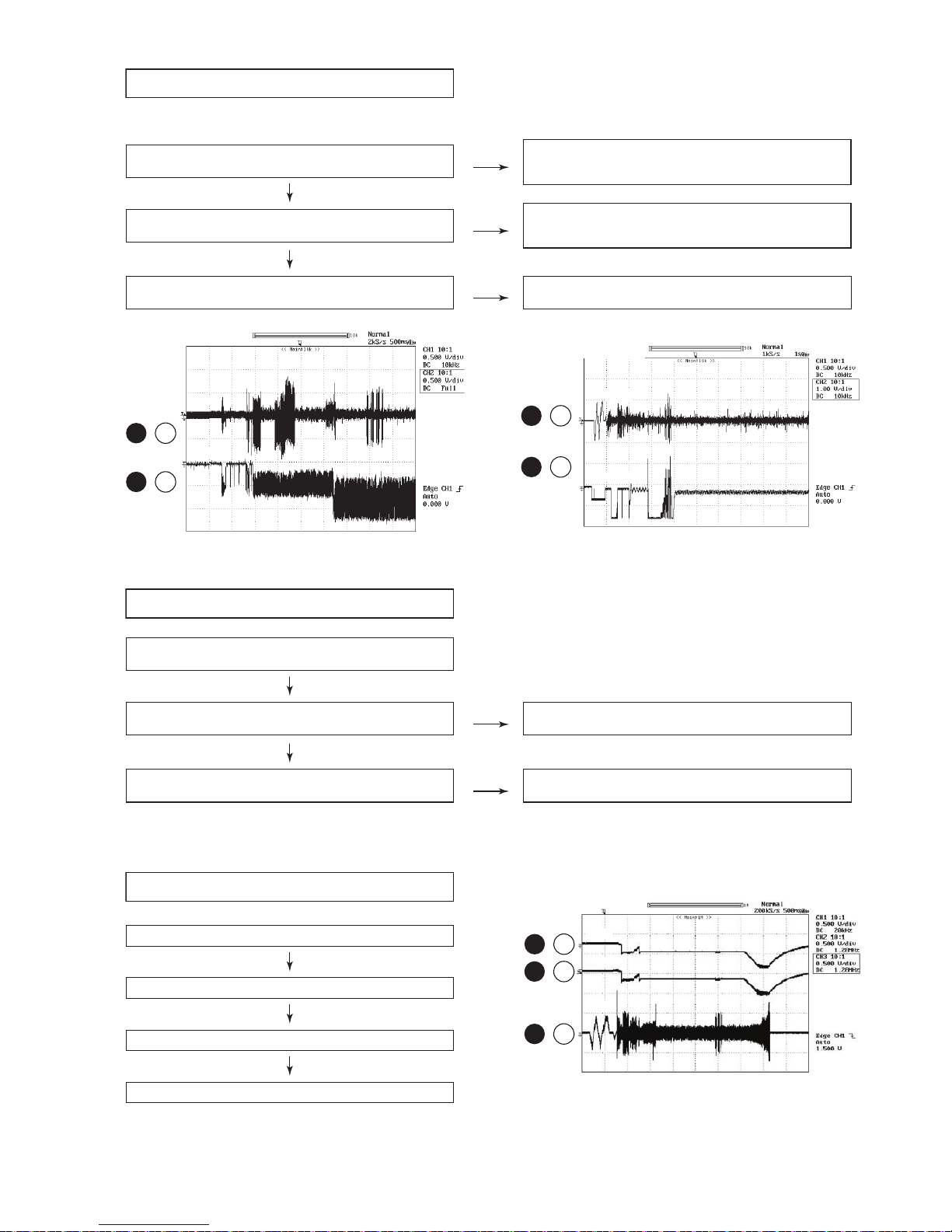
GX-M10
5 – 3
The tracking servo is not activated.
Check the peripheral circuits at pins 50, 51, 48, 49 on IC1 and
FFC1.
(2) Tracking system check.
If the waveform shown in Figure 4 appears and soon after NO
DISC appears ?
Check the TE waveform at pin 63 on IC1.
"Initialization" is possible, but play is not possible ?
No
Yes
A normal jump operation cannot be completed or the begining of
the track cannot be found.
Check the around pin 49 on IC1.
Yes
"Initialization" is not possible.
No
When a disc is loaded, start play operation.
The RF waveform is normal, but the TOC data cannot be read.
Check the PLL waveform. (Figure 6)
Check around pins 73 ~ 76 on IC1.
Data cannot be read. Check the VCO - PLL (Pin no. 73 ~ 76)
on IC1 system.
(3) Spin system check.
(4) PLL system check.
Press the OPEN/CLOSE switch without inserting a disc, and
then try starting the play operation.
1. The turntable rotates a little ?
(Waveform drawing Figure 5)
Yes
2. The turntable does not rotate.
The spin driver circuit is OK.
Check around pin 50 on IC1, pins 1 and 2 on CNP2.
No
Figure 4
138
67
IC1
IC1
4
TE
RFOUT
7
48
50
IC1
IC1
1
FOP
SPOUT
3
74
75
IC1
IC1
5
PLLF
PLLFO
6
48
IC1
FOP
1
Figure 5
Figure 6
Page 18
GX-M10
6 – 1
CHAPTER 6. MAJOR PART DRAWING
[1] Function Table Of IC
IC600 CH-IXA369AWA5 : Micro Computer IXA369AW00 ( 1/4 )
Pin
No.
NAME
INPUT/
OUTPUT
TYPE
SOFT
PULL-UP
DESCRIPTION
HARDWARE
PULL-UP
PORT_TYPE
1
HP_SEL
INPUT
CMOS INPUT /
OUTPUT
OFF
HEADPHONE IN DETECTION SWITCH
L : IN , H : OUT
NEED
P3_3/SSI
2
TUN_SDA/DAP_SDA
INPUT /
OUTPUT
CMOS INPUT /
OUTPUT
OFF TUNER/DAP DATA I2C BUS LINE NEED
P3_4/SDA/SCS
3
MODE
INPUT INPUT - CONNECT THIS PIN TO VCC VIA A RESISTOR NEED
MODE
4
XCIN
INPUT
CMOS INPUT /
OUTPUT
OFF 32.768kHz CRYSTAL (SUB CLOCK)
P4_3/XCIN
5
XCOUT
OUTPUT
CMOS INPUT /
OUTPUT
OFF 32.768kHz CRYSTAL (SUB CLOCK)
P4_4/XCOUT
6
RESET
INPUT INPUT -
RESET INPUT. ACTIVE "L"
CONNECT TO WRITER RESET LINE DURING
FLASH
NEED
RESET
7
XOUT
OUTPUT INPUT OFF 8MHz CERAMIC OSCILLATOR (MAIN CLOCK)
P4_7/XOUT(Note1)
8
VSS
-- -GROUND
VSS/AVSS
9
XIN
INPUT INPUT OFF 8MHz CERAMIC OSCILLATOR (MAIN CLOCK)
P4_6/XIN
10
VCC
- - - 3.3V SUPPLY
VCC/AVCC
11
DAP_RST
OUTPUT
CMOS INPUT /
OUTPUT
OFF
DAP RESET CONTROL
H : NORMAL , L : RESET
P5_4/TRCIOD
12
DAP_PWDN
OUTPUT
CMOS INPUT /
OUTPUT
OFF
DAP POWER DOWN CONTROL
H : NORMAL , L : POWER DOWN
P5_3/TRCIOC
13
DAP_MUTE
OUTPUT
CMOS INPUT /
OUTPUT
OFF
DAP MUTE CONTROL
H : MUTE OFF , L : MUTE ON
P5_2/TRCIOB
14
DCDC_EN
OUTPUT
CMOS INPUT /
OUTPUT
OFF
12V SUPPLY CONTROL, ON DURING DEMO/P-ON
H : ON; L : OFF
P5_1/TRCIOA/TRCTRG
15
DC_ECO
OUTPUT
CMOS INPUT /
OUTPUT
OFF
ECO CTRL
H: OTHERS , L: DC DEMO OFF
P5_0/TRCCLK
16
LCD_CE
OUTPUT
CMOS INPUT /
OUTPUT
OFF LCD DRIVER CHIP ENABLE OUTPUT
P2_7/TRDIOD1
17
LCD_BCKLGHT
OUTPUT
CMOS INPUT /
OUTPUT
OFF
LCD BACKLIGHT CONTROL
L : OFF H: ON
P2_6/TRDIOC1
18
IPOD_DET
INPUT
CMOS INPUT /
OUTPUT
OFF
IPOD IN DETECTION
L : IN , H : OUT
NEED
P2_5/TRDIOB1
19
FAULT
INPUT
CMOS INPUT /
OUTPUT
OFF CURRENT LIMITTER IC ERROR DETECT NEED
P2_4/TRDIOA1
20
USB_EN
OUTPUT
CMOS INPUT /
OUTPUT
OFF
CURRENT LIMITTER IC SELECTOR
H:USB L:OTHERS
P2_3/TRDIOD0
21
IPOD_EN
OUTPUT
CMOS INPUT /
OUTPUT
OFF
CURRENT LIMITTER IC SELECTOR
H:IPOD L:OTHERS
P2_2/TRDIOC0
22
GUI_MUTE
OUTPUT
CMOS INPUT /
OUTPUT
OFF
GUITAR MUTE CONTROL
L : MUTE ON , H : MUTE OFF
P2_1/TRDIOB0
23
DSEL_S
OUTPUT
CMOS INPUT /
OUTPUT
OFF
D+/D- BUS SELECTOR CONTROL
H : IPOD , L : USB
P2_0/TRDIOA0/TRDCLK
24
RX_IN
INPUT
CMOS INPUT /
OUTPUT
OFF REMOCON SENSOR INPUT
P1_7/TRAIO/INT1
25
LCD_CLK
OUTPUT
CMOS INPUT /
OUTPUT
OFF LCD DRIVER CLOCK OUTPUT
P1_6/CLK0
26
MIC_MUTE
OUTPUT
CMOS INPUT /
OUTPUT
OFF
MIC MUTE CONTROL
L : MUTE ON , H : MUTE OFF
P1_5/RXD0/(TRAIO)/
(INT1)(Note2)
Page 19

GX-M10
6 – 2
27
LCD_DI
OUTPUT
CMOS INPUT /
OUTPUT
OFF LCD DRIVER DATA OUTPUT
P1_4/TXD0
28
MIC_SW
INPUT
CMOS INPUT /
OUTPUT
OFF
MIC IN DETECTION SWITCH
H : IN , L : OUT
NEED
P8_6
29
GUITAR_SW
INPUT
CMOS INPUT /
OUTPUT
OFF
GUITAR IN DETECTION SWITCH
H : IN , L : OUT
NEED
P8_5/TRFO12
30
CD_DOOR_SW
INPUT
CMOS INPUT /
OUTPUT
OFF
CD DOOR OPEN/CLOSE DETECTION SWITCH
L: CLOSE; H: OPEN
NEED
P8_4/TRFO11
31
CURRENT_LIMIT
OUTPUT
CMOS INPUT /
OUTPUT
OFF CURRENT LIMITTER IC SET
P8_3/TRFO10/TRFI
32
A_MUTE
INPUT
CMOS INPUT /
OUTPUT
OFF A MUTE INPUT
P8_2/TRFO02
33
LED_FLSH_CTR
OUTPUT
CMOS INPUT /
OUTPUT
OFF
SUBWOOFER SPEAKER LED FLASHING CTRL
H: ON L: OFF
P8_1/TRFO01
34
USB_IN
INPUT
CMOS INPUT /
OUTPUT
OFF
USB DETECTION
H : DETACH , L : ATTACH
P8_0/TRFO00
35
CD_MREQ
OUTPUT
CMOS INPUT /
OUTPUT
OFF DATA TRANSMISSION REQUEST TO CD DSP
P6_0/TREO
36
SYS_STOP
INPUT
CMOS INPUT /
OUTPUT
OFF POWER FAILURE DETECTION NEED
P4_5/INT0
37
CD_SREQ
INPUT
CMOS INPUT /
OUTPUT
OFF DATA TRANSMISSION REQUEST TO CD DSP
P6_6/INT2/TXD1
38
LED_CTR
OUTPUT
CMOS INPUT /
OUTPUT
OFF
LED FLASH ON/OFF CTRL
L : OFF , H : ON
P6_7/INT3/RXD1
39
CD_SCLK
OUTPUT
CMOS INPUT /
OUTPUT
OFF
DATA TRANSMISSION/RECEPTION SYNCHRONOUS CLOCK TO CD DSP
P6_5/(CLK1)/
CLK2(Note2)
40
CD_SO
INPUT
CMOS INPUT /
OUTPUT
OFF DATA OUTPUT FROM CD DSP
P6_4/RXD2
41
CD_SI
OUTPUT
CMOS INPUT /
OUTPUT
OFF DATA INPUT TO CD DSP
P6_3/TXD2
42
CD_RST
OUTPUT
CMOS INPUT /
OUTPUT
OFF CD DSP RESET
P3_1/TRBO
43
AMP_OTW
INPUT
CMOS INPUT /
OUTPUT
OFF
AMPLIFIER OVERTEMPERATURE WARNING
DETECTION
H : NORMAL , L : ABNORMAL
NEED
P3_0/TRAO
44
AMP_SD
INPUT
CMOS INPUT /
OUTPUT
OFF
AMPLIFIER SHUTDOWN DETECTION
H : NORMAL , L : ABNORMAL
NEED
P3_6/(INT1)(Note2)
45
IN_SO
OUTPUT
CMOS INPUT /
OUTPUT
OFF INPUT SELECTOR CONTROL 0
P3_2/(INT2)(Note2)
46
IN_S1
OUTPUT
CMOS INPUT /
OUTPUT
OFF INPUT SELECTOR CONTROL 1
P1_3/Kl3/AN11
47
TUN_RST
OUTPUT
CMOS INPUT /
OUTPUT
OFF TUNER RESET
P1_2/Kl2/AN10
48
BATT_LEV Input
(Analog/
Digital)
CMOS INPUT /
OUTPUT
OFF BATTERY LEVEL INPUT DETECTION
P1_1/Kl1/AN9
49
KEY_6 Input
(Analog/
Digital)
CMOS INPUT /
OUTPUT
OFF
KEY5 LINE A/D DETECTION
H : KEY OFF
NEED
P1_0/Kl0/AN8
50
KEY_ IPOD
INPUT
CMOS INPUT /
OUTPUT
OFF
IPOD PLAY/PAUSE
H : KEY OFF
NEED
P0_0/AN7
51
KEY_ CD
INPUT
CMOS INPUT /
OUTPUT
OFF
CD PLAY/PAUSE
H : KEY OFF
NEED
P0_1/AN6
52
KEY_ USB
INPUT
CMOS INPUT /
OUTPUT
OFF
USB PLAY/PAUSE
H : KEY OFF
NEED
P0_2/AN5
53
KEY_ TUNER
INPUT
CMOS INPUT /
OUTPUT
OFF
TUNER/AUDIO IN
H : KEY OFF
NEED
P0_3/AN4
54
KEY_ POWER
INPUT
CMOS INPUT /
OUTPUT
OFF
ON/STANDBY
H : KEY OFF
NEED
P0_4/AN3
Pin
No.
NAME
INPUT/
OUTPUT
TYPE
SOFT
PULL-UP
DESCRIPTION
HARDWARE
PULL-UP
PORT_TYPE
IC600 CH-IXA369AWA5 : Micro Computer IXA369AW00 ( 2/4 )
Page 20

GX-M10
6 – 3
55
TIMER_LED
OUTPUT
CMOS INPUT /
OUTPUT
OFF
TIMER LED CONTROL
H : ON , L : OFF
P6_2
56
AC_RELAY
OUTPUT
CMOS INPUT /
OUTPUT
OFF
MAIN TRANS ON/OFF CONTROL
H : POWER ON/DEMO ,
L : POWER OFF/ECO/DC MODE
P6_1
57
LEVEL_DET Input
(Analog/
Digital)
CMOS INPUT /
OUTPUT
OFF ANALOG AUDIO LEVEL INPUT A/D DETECTION
P0_5/AN2/CLK1
58
AREA Input
(Analog/
Digital)
CMOS INPUT /
OUTPUT
OFF DESTINATION SETTING A/D INPUT NEED
P0_6/AN1/DA0
59
VSS
-- -GROUND
VSS/AVSS
60
SYS_PROTECT Input
(Analog/
Digital)
CMOS INPUT /
OUTPUT
OFF SUPPLY ABNORMAL A/D DETECTION NEED
P0_7/AN0/DA1
61
VREF
- - - A/D CONVERTER REFERENCE VOLTAGE SUPPLY
VREF
62
VCC
- - - 3.3V SUPPLY
VCC/AVCC
63
HP_MUTE
OUTPUT
CMOS INPUT /
OUTPUT
OFF
HEADPHONE MUTE CONTROL
H : ON , L : OFF
P3_7/SSO
64
TUN_SCL/DAP_SCL
OUTPUT
CMOS INPUT /
OUTPUT
OFF TUNER/DAP CLOCK I2C BUS LINE
P3_5/SCL/SSCK
Note1. P4_7/XOUT is INPUT port.
Note2. ( ) port can be allocated by program.
Pin
No.
NAME
INPUT/
OUTPUT
TYPE
SOFT
PULL-UP
DESCRIPTION
HARDWARE
PULL-UP
PORT_TYPE
IC600 CH-IXA369AWA5 : Micro Computer IXA369AW00 ( 3/4 )
Page 21

GX-M10
6 – 4
IC600 CH-IXA369AWA5 : Micro Computer IXA369AW00 ( 4/4 )
㼀㼁㻺㼋㻿㻯㻸㻛㻰㻭㻼㼋㻿㻯㻸
㻴㻼㼋㻹㼁㼀㻱
㼂㻯㻯
㼂㻾㻱㻲
㻿㼅㻿㼋㻼㻾㻻㼀㻱㻯㼀
㼂㻿㻿
㻭㻾㻱㻭
㻸㻱㼂㻱㻸㼋㻰㻱㼀
㻭㻯㼋㻾㻱㻸㻭㼅
㼀㻵㻹㻱㻾㼋㻸㻱㻰
㻷㻱㼅㼋㻌㻌㻼㻻㼃㻱㻾
㻷㻱㼅㼋㻌㼀㼁㻺㻱㻾
㻷㻱㼅㼋㻌㼁㻿㻮
㻷㻱㼅㼋㻌㻯㻰
㻷㻱㼅㼋㻌㻵㻼㻻㻰
㻷㻱㼅㼋㻢
㻢㻠
㻢㻟
㻢㻞
㻢㻝
㻢㻜
㻡㻥
㻡㻤
㻡㻣
㻡㻢
㻡㻡
㻡㻠
㻡㻟
㻡㻞
㻡㻝
㻡㻜
㻠㻥
㻼㻟㼋㻡㻛㻿㻯㻸㻛㻿㻿㻯
㻷
㻼㻟㼋㻣㻛㻿㻿㻻
㼂㻯㻯㻛㻭㼂㻯㻯
㼂㻾㻱㻲
㻼㻜㼋㻣㻛㻭㻺㻜㻛㻰㻭㻝
㼂㻿㻿㻛㻭㼂㻿㻿
㻼㻜㼋㻢㻛㻭㻺㻝㻛㻰㻭㻜
㻼㻜㼋㻡㻛㻭㻺㻞㻛㻯㻸㻷㻝
㻼㻢㼋㻝
㻼㻢㼋㻞
㻼㻜㼋㻠㻛㻭㻺㻟
㻼㻜㼋㻟㻛㻭㻺㻠
㻼㻜㼋㻞㻛㻭㻺㻡
㻼㻜㼋㻝㻛㻭㻺㻢
㻼㻜㼋㻜㻛㻭㻺㻣
㻼㻝㼋㻜㻛㻷㼘㻜㻛㻭㻺㻤
㻴㻼㼋㻿㻱㻸
㻝 㻼㻟㼋㻟㻛㻿㻿㻵 㻼㻝㼋㻝㻛㻷㼘㻝㻛㻭㻺㻥 㻠㻤
㻮㻭㼀㼀㼋㻸㻱㼂
㼀㼁㻺㼋㻿㻰㻭㻛㻰㻭㻼㼋㻿㻰㻭
㻞 㻼㻟㼋㻠㻛㻿㻰㻭㻛㻿㻯㻿 㻼㻝㼋㻞㻛㻷㼘㻞㻛㻭㻺㻝㻜 㻠㻣
㼀㼁㻺㼋㻾㻿㼀
㻹㻻㻰㻱
㻟 㻹㻻㻰㻱 㻼㻝㼋㻟㻛㻷㼘㻟㻛㻭㻺㻝㻝 㻠㻢
㻵㻺㼋㻿㻝
㼄㻯㻵㻺
㻠 㻼㻠㼋㻟㻛㼄㻯㻵㻺
P3_2/(INT2)(Note2
㻠㻡
㻵㻺㼋㻿㻻
㼄㻯㻻㼁㼀
㻡 㻼㻠㼋㻠㻛㼄㻯㻻㼁㼀
P3_6/(INT1)(Note2
㻠㻠
㻭㻹㻼㼋㻿㻰
㻾㻱㻿㻱㼀
㻢 㻾㻱㻿㻱㼀 㻼㻟㼋㻜㻛㼀㻾㻭㻻 㻠㻟
㻭㻹㻼㼋㻻㼀㼃
㼄㻻㼁㼀
㻣 㻼㻠㼋㻣㻛㼄㻻㼁㼀㻔㻺㼛㼠㼑㻝㻕 㻼㻟㼋㻝㻛㼀㻾㻮㻻 㻠㻞
㻯㻰㼋㻾㻿㼀
㼂㻿㻿 㻤 㼂㻿㻿㻛㻭㼂㻿㻿 㻼㻢㼋㻟㻛㼀㼄㻰㻞 㻠㻝
㻯㻰㼋㻿㻵
㼄㻵㻺
㻥 㻼㻠㼋㻢㻛㼄㻵㻺 㻼㻢㼋㻠㻛㻾㼄㻰㻞 㻠㻜
㻯㻰㼋㻿㻻
㼂㻯㻯 㻝㻜 㼂㻯㻯㻛㻭㼂㻯㻯
㻼㻢㼋㻡㻛㻔㻯㻸㻷㻝㻕㻛㻯㻸㻷
㻞㻔㻺㼛㼠㼑㻞㻕
㻟㻥
㻯㻰㼋㻿㻯㻸㻷
㻰㻭㻼㼋㻾㻿㼀
㻝㻝 㻼㻡㼋㻠㻛㼀㻾㻯㻵㻻㻰 㻼㻢㼋㻣㻛㻵㻺㼀㻟㻛㻾㼄㻰㻝 㻟㻤
㻸㻱㻰㼋㻯㼀㻾
㻰㻭㻼㼋㻼㼃㻰㻺
㻝㻞 㻼㻡㼋㻟㻛㼀㻾㻯㻵㻻㻯 㻼㻢㼋㻢㻛㻵㻺㼀㻞㻛㼀㼄㻰㻝 㻟㻣
㻯㻰㼋㻿㻾㻱㻽
㻰㻭㻼㼋㻹㼁㼀㻱
㻝㻟 㻼㻡㼋㻞㻛㼀㻾㻯㻵㻻㻮 㻼㻠㼋㻡㻛㻵㻺㼀㻜 㻟㻢
㻿㼅㻿㼋㻿㼀㻻㻼
㻰㻯㻰㻯㼋㻱㻺
㻝㻠 㻼㻡㼋㻝㻛㼀㻾㻯㻵㻻㻭㻛㼀㻾㻯㼀㻾㻳 㻼㻢㼋㻜㻛㼀㻾㻱㻻 㻟㻡
㻯㻰㼋㻹㻾㻱㻽
㻰㻯㼋㻱㻯㻻
㻝㻡 㻼㻡㼋㻜㻛㼀㻾㻯㻯㻸㻷 㻼㻤㼋㻜㻛㼀㻾㻲㻻㻜㻜 㻟㻠
㼁㻿㻮㼋㻵㻺
㻸㻯㻰㼋㻯㻱
㻝㻢 㻼㻞㼋㻣㻛㼀㻾㻰㻵㻻㻰㻝 㻼㻤㼋㻝㻛㼀㻾㻲㻻㻜㻝 㻟㻟
㻸㻱㻰㼋㻲㻸㻿㻴㼋㻯㼀㻾
㻼㻞㼋㻢㻛㼀㻾㻰㻵㻻㻯㻝
㻼㻞㼋㻡㻛㼀㻾㻰㻵㻻㻮㻝
㻼㻞㼋㻠㻛㼀㻾㻰㻵㻻㻭㻝
㻼㻞㼋㻟㻛㼀㻾㻰㻵㻻㻰㻜
㻼㻞㼋㻞㻛㼀㻾㻰㻵㻻㻯㻜
㻼㻞㼋㻝㻛㼀㻾㻰㻵㻻㻮㻜
㻼㻞㼋㻜㻛㼀㻾㻰㻵㻻㻭㻜㻛
㼀㻾㻰㻯㻸㻷
㻼㻝㼋㻣㻛㼀㻾㻭㻵㻻㻛㻵㻺㼀㻝㻼㻝㼋㻢㻛㻯㻸㻷㻜
㻼㻝㼋㻡㻛㻾㼄㻰㻜㻛㻔㼀㻾
㻭㻵㻻㻕㻛㻔㻵㻺㼀㻝㻕㻔㻺㼛㼠㼑
㻼㻝㼋㻠㻛㼀㼄㻰㻜
㻼㻤㼋㻢
㻼㻤㼋㻡㻛㼀㻾㻲㻻㻝㻞
㻼㻤㼋㻠㻛㼀㻾㻲㻻㻝㻝
㻼㻤㼋㻟㻛㼀㻾㻲㻻㻝㻜㻛㼀
㻾㻲㻵
㻼㻤㼋㻞㻛㼀㻾㻲㻻㻜㻞
㻝㻣
㻝㻤
㻝㻥
㻞㻜
㻞㻝
㻞㻞
㻞㻟
㻞㻠
㻞㻡
㻞㻢
㻞㻣
㻞㻤
㻞㻥
㻟㻜
㻟㻝
㻟㻞
㻸㻯㻰㼋㻮㻯㻷㻸㻳㻴㼀
㻵㻼㻻㻰㼋㻰㻱㼀
㻲㻭㼁㻸㼀
㼁㻿㻮㼋㻱㻺
㻵㻼㻻㻰㼋㻱㻺
㻳㼁㻵㼀㼋㻹㼁㼀㻱
㻰㻿㻱㻸㼋㻿
㻾㼄㼋㻵㻺
㻸㻯㻰㼋㻯㻸㻷
㻹㻵㻯㼋㻹㼁㼀㻱
㻸㻯㻰㼋㻰㻵
㻹㻵㻯㼋㻿㼃
㻳㼁㻵㼀㻭㻾㼋㻿㼃
㻯㻰㼋㻰㻻㻻㻾㼋㻿㼃
㻯㼁㻾㻾㻱㻺㼀㼋㻸㻵㻹㻵㼀
㻭㼋㻹㼁㼀㻱
Figure 6-1 BLOCK DIAGRAM OF IC
IXA369AW
Page 22

GX-M10
6 – 5
[2] LCD Display
LCD701 RV-LXA009AWZZ
GRID ASSIGNMENT
ANODE CONNECTION
Page 23

GX-M10
6 – 6
-MEMO-
Page 24

GX-M10
7 – 1
CHAPTER 7. DIAGRAMS
[1] Main Block Diagram
Figure 7-1: MAIN BLOCK DIAGRAM
R+
L+
R-
L-
3Ω
17W
3Ω
17W
Front speaker-R
Front speaker-L
Subwoofer
6Ω
33W
Subwoofer
S
ubwoofer
LED Flash
33W
6Ω
CD/MP3
ANALOG
MULTIPLEXER
CD4052B
ADC IC
PCM1808
BCLK
LRCK
MCLK / SCK
DOUT
D+
D-
D+
D-
1
2
1
2
TS3USB
221A
MN6627992AB
CD / MP3 / USB / iPod
D+
D-
D+
D-
D+
D-
A~
F
SRDATAT
BCLK
LRCK
MCLK
DAP
TAS5504A
SDIN2
SCLK
LRCK
MCLK
INL
INR
LCH
RCH
L-CH
R-CH
L-ch
L-ch
R-ch
R-ch
L / R Ch
L / R Ch
MICOM IC
IX-364AW
(R5F212ACSNFP)
SCL
SDA
SDA
S
CL
SDA
SCL
S
CL
SDA
SDIN1
HEADPHONE
OP-AMP
UTC4580E
LEVEL DETECT
OP-AMP
LVL DET
LEVEL DETECT
PWM_P_1
PWM_M_4
PWMP4
PWM_HPMR
PWM_HPPR
PWM_P_2
PWMD
PWMC
PWMB
PWMA
L-CH
R-CH
DVDD
U
SB
AVDD
Vcc
US
BDP
U
S
BDM
LRCKI
BCLKI
DATAI
MCLKI
PWM_HPML
PWM_HPPL
MIC OP-AMP
UTC4580D
L-CH
R-CH
SDRAM
OUT_C
OUT_D
OUT_A
OUT_B
GVDD
PVDD
VDD
MIXER OP-AMP
UTC4580E
UTC4580E
HP_SEL
HEADPHONE
32Ω
323
4
7
111
106
8
5
3
13
16
13
14
14
1
2
3
56
30
27
26
63
24
25
12
52
51
43
41
6
8
16
18
59
60
61
62
5
6
3
2
8
7
6
31
9
64
2
32
2
15
M
IC590
MFI335S3959
IC3
MIXED INPUT
(MONO )
MIC OP-AMP
UTC4580D
IC2
SA5888
CD DRIVER IC
EM638165
TPS2561D
CD MOTOR
IC1
IC6
W25Q16BV
IC7
IC461
IC451
IC401
IC600
IC900
IC500
IC550
IC580
IC4
78
79
IC5
124
10
+5V
+3.3V
+3.3V
+5V
+3.3V
LED FLASH
CTRL
Vcc
Vcc
Vcc
Vcc
AC RLY
PWR_ON_AC RLY
SMPS PWB-B
(Not Serviceable Item)
RUiTZA056AWZZ
+3.3V
L-ch
R-ch
TAS5342LA
POWER AMP IC
+3.3V
MP2303A
DA1010
IC802
2
2
4
3
MP2303A
IC804
2 3
+22V
UN_SW +4.5V
Power Supply
Audio Signal
MC33063A
IC803
6
1
+12V
+12V
+3.9V
+3.3V
+12V
+12V
12V
5V
BA00BWFP
IC801
3.9V
5V
3464A33
IC805
3.3V
iPod
TERMINAL
U
SB HO
ST
3
4
Vcc
Vdd
GUITAR
INPUT JACK
MIC
INPUT JACK
VIDEO
INPUT JACK
TUNER IN
AUDIO IN
IC401
+5V
+5V
CD Driver IC
Supply (IC2)
iPod / USB Supply (IC5)
+3.3V
AUDIO_CLK /
117
116
115
118
123
125
57
+12V
+12V
BATTERY TERMINAL
15V
(UM / SUM-1,R20) X 10
DC12V
GS1GCTP
62
SDA
SCL
+3.3V
+5V
FLASH MEMORY IC
Page 25

GX-M10
7 – 2
-MEMO-
Page 26

GX-M10
– 1
-MEMO-
7 – 3
Page 27

GX-M10
8 – 1
CHAPTER 8. CIRCUIT SCHEMATICS AND PARTS LAYOUT
[1] Notes On Schematic Diagram
[2] Types Of Transistor And LED
••
•
Resistor:
To differentiate the units of resistors, such symbol as
K and M are used: the symbol K means 1000 ohm
and the symbol M means 1000 kohm and the
resistor without any symbol is ohm-type resistor.
Besides, the one with “Fusible” is a fuse type.
Capacitor:
To indicate the unit of capacitor, a symbol P is used:
this symbol P means pico-farad and the unit of the
capacitor without such a symbol is microfarad. As to
electrolytic capacitor, the expression “capacitance/
withstand voltage is used”.
(CH), (TH), (RH), (UJ): Temperature compensation
(ML): Mylar type
(P.P.): Polypropylene type
Schematic diagram and Wiring Side of P.W.Board
for this model are subject to change for
improvement without prior notice.
•
•
The indicated voltage in each section is the one
measured by Digital Multimeter between such a
section and the chassis with no signal given.
Parts marked with “ ” ( ) are
important for maintaining the safety of the set. Be
sure to replace these parts with specified ones for
maintaining the safety and performance of the set.
PWB Switch Location
REF. NO
SW700
SW701
SW702
TUNER/AUDIO IN
USB
iPod
CD
SW703
DEMO/DIMMER
SW704
SW705
X-BASS/EQ
ONON
ON OFF
ON
OFFON
ONON
ONON
OFF
POSITION ON.FERNOITPIRCSED
SW706
SW707
SW708
PRESET DOWN
PRESET UP
ON/STANDBY
VOLUME DOWN
SW709
VOLUME UP
SW710
ON OFF
VOL
OFFON
MIN
VOL
MAX
POSITIONDESCRIPTION
ON OFF
1. In the tuner section,
2. In the CD section, the CD is stopped.
indicates AM
indicates FM stereo
TO
P
VIEW
T
O
P
VIEW
T
O
P
VIEW
DA1010++
FRONT
VIEW
KTC3875GR
KTC2875
MPS8550S
KRC102S
KRC104S
KTA1504
B
(2)
E
(1)
TOP
VIEW
2SK3018 PST8227U
G
(2)
S
(1)
DC
(3)(3)
TOP
VIEW
KTA1271Y
KTC3205
VIEW
FRONT
ECB
(1)(2)(3)
343VC3F
EXA694WJ
EXA701W
EXA718WJ
RB080L30
1
(G)
(S)
(D)
2
3
SSM3J332R
Page 28

GX-M10
8 – 2
[3] Schematic Diagram
Figure 8-1: MAIN SECTION SCHEMATIC DIAGRAM (1/2)
MAIN PWB-A1
(Not Serviceable Item)
SMPS PWB-B
CN1
CN2
1234567
BATTERY TERMINAL PWB
AUDIO SIGNAL
SIGNAL FLOW
NC
NC
NC
MIC IN
GUITAR IN
RB521
470/16
470/16
470/16
470/16
5.0A, 32 VDC
7
8 9101112
A
B
C
D
E
F
G
H
1
2 3 456
Page 29

GX-M10
8 – 3
Figure 8-2: MAIN SECTION SCHEMATIC DIAGRAM (2/2)
AUDIO SIGNAL
SIGNAL FLOW
TUNER SIGNAL
FROM
FROM DISPLAY PWB-C1
MICOM
REFLASH TERMINAL
CNP701
SILICON TUNER PACK
RTUNSA047AWZZ
( )
7
8 9101112
A
B
C
D
E
F
G
H
1
2 3 456
Page 30

GX-M10
8 – 4
Figure 8-3: MAIN (CD SERVO) SECTION SCHEMATIC DIAGRAM
MAIN PWB-A1
CD SERVO SECTION
FROM
CD PICK UP
UNIT
MICOM
REFLASH TERMINAL
TO
USB PWB-C3
CNP781
TO
iPod PWB-A2
CNP201
CD DSP FLASH MEMORY IC
7
8 9101112
A
B
C
D
E
F
G
H
1
2 3 456
Page 31

GX-M10
8 – 5
Figure 8-4: DISPLAY, KEY & TIMER SECTION SCHEMATIC DIAGRAM
DISPLAY PWB-C1
Timer Section
TO
MAIN SECTION
KEY PWB-C2
VERSION
ORANGE (OR)
RED (RD)
LCD BACKLIGHT PANEL R722 R723
100Ω 100Ω
150
Ω 150
Ω
HDECQA649AW01
GUN METAL (GM) 100Ω 100ΩHDECQA649AW01
HDECQA681AW01
SELECTION TABLE
7
8 9101112
A
B
C
D
E
F
G
H
1
2 3 456
Page 32

GX-M10
8 – 6
Figure 8-5: iPod, TRANSIT (Subwoofer Flash, USB Battery & AC Inlet) SECTION SCHEMATIC DIAGRAM
U
SB PWB-C
3
FOR
USB EXTERNAL
DEVICE ONLY
FROM
MAIN PWB-A1
Bi4
iPod PWB-A2
TRANSIT PWB-C4
SUBWOOFER FLASHING SECTION
H
C-LHC-
R
BATTERY TERMINAL 1 & 2
AC INLET PWB-C9
TO
MAIN PWB-A1
TO
MAIN PWB-A1
FOR
IPOD EXTERNAL
DEVICE ONLY
AC POWER S
UPPLY CORD
QACCD0025AWZZ
AC120 ~ 60Hz
SMP
S
PWB-B
TO
MAIN PWB-A
1
2
1
2
(Not Serviceable Item)
CN1
407SNC507SNC
USB
SIGNAL FLOW
VIDEO
Bi2
CN2
12
34567
FROM
MAIN PWB-A
Bi901
JP252 RBLN-0081
JP250 RBLN-0081
C060AW
RD
OR
GM
LED704
i343YC i343YC i343YC i343YC
i343YC i343YC i343YC i343YC
M3NR2UDO M3NR2UDO M3NR2UDO M3NR2UDO
LED705 LED706 LED707
SELECTION TABLE FOR
S
UBWOOFER FLA
S
HING
VERSION
VERSION
220Ω
OR
R790
18
0Ω
Ω
220
Ω
R791
180Ω
220
Ω
R792
180
Ω
220
Ω
R79
3
180
Ω
GM
RD
180180Ω 180Ω180
Ω
REFER
SELECTION TABLE FOR PARTS
MARKED WITH (*)
7
8 9101112
A
B
C
D
E
F
G
H
1
2 3 456
RD = RED
OR = ORANGE
GM = GUN METAL
Page 33

GX-M10
8 – 7
[4] Chart Of Connecting Wires
Figure 8-6: WIRING CONNECTION
RD
BK
WH
RED
BLACK
WHITE
GY GRAY
BL BLUE
BR BROWN
PK PINK
YL YELLOW
COLOR TABLE
CNP201
CNP200
1
LUG200
Bi702
CNS702
CNP702A
LCD701
CNP701
FOR
CONNECT
TO
CHASSIS
CONNECT
TO
CHASSIS
CONNECT
TO
CHASSIS
iPod EXTERNAL
DEVICE ONLY
FOR
USB EXTERNAL
DEVICE ONLY
1
2
3
4
5
6
7
123
45678
9
1
Bi701B
RDWHRD
WH
RD
BL
WHRDWH
Bi701A
2345
101112
13 15
14
12345
DISPLAY PWB-C1
KEY PWB-C2
US
B PWB-C3
AC INLET PWB-C9
SMPS PWB-B
MAIN PWB-A1
(Not Replacement Item)
DOOR
SWITCH
PWB-A3
TRANS
IT
PWB-C4
SUBWOOFER FLA
SH (R-CH) PWB-C6
30
1
Bi705
BK
RD
BK
RD
CNS901B CNS705
CNS704
CNS701A
A107SNC
A
109SNC
FFC1
CNS2A
CNS2B
12
S
UBWOOFER FLASH (L-CH) PWB-C5
Bi704
12
CNP701B
FFC702
FFC702
FFC701
FFC701
357
246
ADAPTOR IN
12VDC
JK801
HEADPHONE
JK550
AUDIO IN
JK570
ANTENNA IN
TUN301
MICOM REFLASH
TERMINAL
CNP600
VIDEO OUT
JK571
LUG
803
MIC VOLUME
VR401
GUITAR VOLUME
VR431
MIC IN
MIC401
GUITAR IN
GUT431
CNP802
CNS904
Bi904
Bi903
BL BR
BR
BL
CNS801
112
1
BL
RD
2
2
SO901
RD
RD
RD
Bi901
CNP901
CNP902
DSP
REFLASH TERMINAL
CNP3
2
PNC1PNC
CNP702
LUG782
Bi250
CNS250
JK781
CNP781
CNP701
LUG701
LUG602
LUG601
LUG603
B
CNP
801
Bi801
PLT
8
01
SPR801
PLT802
SPR
802
BATTERY TERMINAL 2 PWB-C
8
BATTERY TERMINAL 1 PWB-C
7
123456
7
6543
2
1
1234567
65432
1
RD
BKBLBKRDBK
RD
TO
CD MOTOR PWB
WH
BL
WHRDWH
654321
65432
1
654321
67
85432
Bi2
Bi4
1
1234
CNS2
CNS4
1234
1234
5
1
1
2
12
12
2
3
456
7
8
9
8710
911
12
131415
16
65432
1
10
11
12
13
14
15
1234567
1234567
1234567
8
123
123
123
12
12
1
BL
GY
BL
GY
BL
GY
RD
BL
GY
BL
GY
BL
GY
RD
TO
CD PICK UP UNIT
1234 567
1234 567
8
12
12
CN1
CN2
LN
PK
BK
PK
WH
YL
GY
(SHIELD WIRE)
GY (SHIELD WIRE)
WH
BKBLBKBLBK
BK
BL
BK
BL
BK
WH
PK
PK
BK
WH
YL
6754321
6754321
CNP250
PK
WH
WH
BK
BK
PK
WH
BK
BK
GY (SHIELD)
BK
BK
BK
1234 567
AC POWER SUPPLY CORD
AC 120V~60Hz
TO SUBWOOFER
(L-CH)
TO MAIN
(L-CH)
TO SUBWOOFER
(R-CH)
TO MAIN
(R-CH)
CNS901
When Servicing, pay attention as the
area enclosed by
this line( )
is directly connected with AC main
voltage.
iPod PWB-A2
CNS903
CONNECT TO
FM. ROD ANTENNA
CNS301-LUG
WIRE F
CONNECT TO
CHASSIS
CORE 3
(RING WITH
2 TURN)
CORE 1
(RING WITH
2 TURN)
CORE 2
(RING WITH
2 TURN)
LUG902
7
8 9101112
A
B
C
D
E
F
G
H
1
2 3
456
Page 34

GX-M10
8 – 8
[5] Wiring Side Of PWB
Figure 8-7: WIRING SIDE OF MAIN PWB (TOP VIEW)
BCE
1234 56
1234 56
1234 5 67
1234 5678
12
12345
1234567
DC ADAPTOR IN
12V
PHONES MIC
VOLUME
MIC IN GUITAR IN GUITAR
VOLUME
AUDIO
IN
VIDEO
OUT
12
123
12345678
MICOM
REFLASH
TERMINAL
16
15
B
CE
MAIN PWB-A1
Lead-free solder indication
Lead-free solder is used in the MAIN PWB.
Refer to "Precautions for handling lead-free solder" for instructions
and precautions.
7
8
9101112
A
B
C
D
E
F
G
H
1
2
3
456
Page 35

GX-M10
8 – 9
Figure 8-8: WIRING SIDE OF MAIN PWB (BOTTOM VIEW)
MAIN PWB-A1
Lead-free solder indication
Lead-free solder is used in the MAIN PWB.
Refer to "Precautions for handling lead-free solder" for instructions
and precautions.
7
8
9101112
A
B
C
D
E
F
G
H
1
2
3
456
Page 36

GX-M10
8 – 10
Figure 8-9: WIRING SIDE OF iPod & DOOR SWITCH PWB
1234567
12
iPod PWB-A2
Top View
Bottom View
Top View
Bottom View
DOOR SWITCH PWB-A3
Lead-free solder indication
Lead-free solder is used in the iPod & DOOR SWITCH PWB.
Refer to "Precautions for handling lead-free solder" for instructions
and precautions.
7
8
9101112
A
B
C
D
E
F
G
H
1
2
3
456
Page 37

GX-M10
8 – 11
Figure 8-10: WIRING SIDE OF DISPLAY, KEY, USB, TIME, TRANSIT SUBWOOFER FLASH (R/L-CH), BATTERY TERMINAL 1/2 & AC INLET PWB (TOP VIEW)
1234 5
1¡
13579
11 13
2468
10 12 14
15
1357
246
13
21
21
21
57
246
12
21
123
123
4567
1234
1234
5
1234 5
678
DISPLAY PWB-C1
KEY PWB-C2
SUBWOOFER FLASH (R-CH) PWB-C6
SUBWOOFER FLASH (L-CH) PWB-C7
Lead-free solder indication
Lead-free solder is used in the DISPLAY, KEY, USB, TIME, TRANSIT SUBWOOFER FLASH (R/L-CH),
BATTERY TERMINAL 1/2 & AC INLET PWB.
Refer to "Precautions for handling lead-free solder" for instructions and precautions.
7
8
9101112
A
B
C
D
E
F
G
H
1
2
3
456
USB PWB-C3
TRANSIT PWB-C5
AC INLET PWB-C10
BATTERY TERMINAL 1 PWB-C8
BATTERY TERMINAL 2 PWB-C9
TIME PWB-C4
Page 38

GX-M10
8 – 12
Figure 8-11: WIRING SIDE OF DISPLAY, KEY, USB, TIME, TRANSIT SUBWOOFER FLASH (R/L-CH), BATTERY TERMINAL 1/2 & AC INLET PWB (BOTTOM VIEW)
DISPLAY PWB-C1
KEY PWB-C2
SUBWOOFER FLASH (R-CH) PWB-C6
SUBWOOFER FLASH (L-CH) PWB-C7
Lead-free solder indication
Lead-free solder is used in the DISPLAY, KEY, USB, TIME, TRANSIT SUBWOOFER FLASH (R/L-CH),
BATTERY TERMINAL 1/2 & AC INLET PWB.
Refer to "Precautions for handling lead-free solder" for instructions and precautions.
7
8
9101112
A
B
C
D
E
F
G
H
1
2
3
456
USB PWB-C3
TRANSIT PWB-C5
TIME PWB-C4
Page 39

GX-M10
8 – 13
-MEMO-
Page 40

GX-M10
– 1
-MEMO-
8 – 14
Page 41

PARTS GUIDE
GX-M10
Parts marked with " " are important for maintaining the safety of the set. Be sure to replace these parts with specified
ones for maintaining the safety and performance of the set.
!
This document has been published to be used
for after sales service only.
The contents are subject to change without notice.
SHARP CORPORATION
PORTABLE CD STEREO SYSTEM
MODEL
GX-M10 (OR
)
[For U.S.A./Canada]
without suffix : GUN METAL COLOR
(OR) : ORANGE COLOR
(RD) : RED COLOR
GX-M10 (RD
)
GX-M10
CONTENTS
[1] INTEGRATED CIRCUITS
[2] TRANSISTORS
[3] DIODES
[4] COILS
[5] CRYSTALS / VIBRATORS
[6] CAPACITORS
[7] RESISTORS
[8] OTHER CIRCUITRY PARTS
[9] CABINET PARTS /
CD MECHANISM PARTS
[10] ACCESSORIES / PACKING PARTS
[11] P.W.B. ASSEMBLY
Explanation of PWB Assembly parts code category
S Category -- Repair ( Component parts of PWB can be replace and repair, PWB no supply )
X Category -- Replacement ( PWB can not be repair. Component parts no supply )
S.X Category -- Repa ir and Replacement ( PWB can repair and replace )
KG Category -- Revolve repair by Business Center ( Return to Business Center and repair by manufacturer. Component parts no supply )
Explanation of capacitors/resistors parts codes
Capacitors
VCC ....................... Ceramic type
VCK ........................ Ceramic type
VCT ........................ Semiconductor type
VC • • MF ............... Cylindrical type (withoutleadwire)
VC • • MN ............... Cylindrical type (withoutleadwire)
VC • • TV ................ Square type (withoutleadwire)
VC • • TQ ............... Square type (withoutlead wire)
VC • • CY ............... Square type (withoutleadwire)
VC • • CZ ............... Square type (withoutlead wire)
VC•••••••••J..The13th character represents capacity difference.
("J" ±5%, "K" ±10%, "M" ±20%, "N" ±30%,
"C" ±0.25 pF, "D" ±0.5 pF, "Z" +80-20%.)
If there are no indications for the electrolytic capacitors,erroris ±20%.
Resi stors
VRD ....................... Carbon-film type
VRS ........................ Carbon-film type
VRN ....................... Metal-film type
VR • • MF ............... Cylindrical type (withoutleadwire)
VR • • MN ............... Cylindrical type (withoutlead wire)
VR • • TV ................ Square type (withoutlead wire)
VR • • TQ ............... Square type (withoutleadwire)
VR • • CY ............... Square type (withoutleadwire)
VR • • CZ ............... Square type (withoutleadwire)
VR•••••••••J..The13th character represents error.
("J" ±5%, "F" ±1%, "D" ±0.5%.)
If there are no indications for other parts,theresistorsare ±5%
carbon-film type.
Page 42

GX-M10
1
NO. PARTS CODE
PRICE
RANK
NEW
MARK
PA RT
RANK
DESCRIPTION
[1] INTEGRATED CIRCUITS
iC1 VHiMN7992AB-1 AZ CD/USB/iPod DSP
iC2 VHiSA5888TR-1 AG CD Motor Driver, SA5888, 28 Pin
iC3 VHi337S3959-1 AM Apple Authentication IC
iC4 VHiTS3USB++-1 AG USB Switch
iC5 VHiTPS2561D-1 AH Current Limiter Power Switch
iC6 VHiEM638165-1 AR 16 Bit, SDRAM
iC7 RH-iXA347AW00 AL CD DSP Flash Memory IC
iC401 VHiUTC4580E-1 AC Dual Operational Amplifier
iC431 VHiUTC4580E-1 AC Dual Operational Amplifier
iC451 VHiUTC4580E-1 AC Dual Operational Amplifier
iC461 VHiUTC4580E-1 AC Dual Operational Amplifier
iC500 VHiTAS5504A-1 AR Digital Audio PWM
iC550 VHiUTC4580E-1 AC Dual Operational Amplifier
iC580 VHiPCM1808P-1 AH Single Ended Analog
iC590 VHiCD4052BM-1 AE Analog Multiplexer, CD4052
iC600 CH-IXA369AWA5 AV System Microcomputer Ass'y, iXA369AW
iC681 VHiPST8227U-1 AC Reset IC, 2.7V
iC701 VHiPT6533LQ-1 AK LCD Drvier
iC801 VHiBA00BWFP-1 AG Voltage Regulator
iC802 VHiMP2303A+-1 AF DC-DC IC 3A 28V 360Khz
iC803 VHiMC33063A-1 AE DC- DC IC 18V
iC804 VHiMP2303A+-1 AF DC-DC IC 3A 28V 360Khz
iC805 VHi3464A33N-1 AC Voltage Regulator, 3.3V
iC900 VHiTAS5342L-1 AR Digital Amplifier
[2] TRANSISTORS
Q3 VSKTA1271Y/-1 AC Silicon, PNP, KTA1271 Y
Q4 VSKTA1504GR-1 AB Silicon, PNP, KTA1504 GR
Q5 VS2SK3018//-1 AC N Channel SK3018
Q401 VSKTA1504GR-1 AB Silicon, PNP, KTA1504 GR
Q402 VSKRC104S//-1 AC Digital, PNP, KRC104S
Q431 VSKTA1504GR-1 AB Silicon, PNP, KTA1504 GR
Q432 VSKRC104S//-1 AC Digital, PNP, KRC104S
Q461 VSKTA1504GR-1 AB Silicon, PNP, KTA1504 GR
Q462 VSKRC104S//-1 AC Digital, PNP, KRC104S
Q491 VSKTC3205Y/-1 AD Silicon, NPN, KTC3205 Y
Q492 VSKTA1504GR-1 AB Silicon, PNP, KTA1504 GR
Q493 VSKRC104S//-1 AC Digital, PNP, KRC104S
Q494 VSKRC104S//-1 AC Digital, PNP, KRC104S
Q551 VSKTC2875B/-1 AC Silicon, NPN, KTC2875 B
Q552 VSKTC2875B/-1 AC Silicon, NPN, KTC2875 B
Q553 VSKRA102S//-1 AB Digital, NPN, KRA102S
Q554 VSKRC104S//-1 AC Digital, PNP, KRC104S
Q591 VSKTC3875GR-1 AB Silicon, NPN, KTC3875 GR
Q593 VSKTC3875GR-1 AB Silicon, NPN, KTC3875 GR
Q671 VSKRC104S//-1 AC Digital, PNP, KRC104S
Q672 VSKTA1504GR-1 AB Silicon, PNP, KTA1504 GR
Q681 VSKRC104S//-1 AC Digital, PNP, KRC104S
Q682 VSKRC104S//-1 AC Digital, PNP, KRC104S
Q701 VSMPS8050S/-1 AB S8050
Q702 VSKRC104S//-1 AC Digital, PNP, KRC104S
Q801 VSKRC104S//-1 AC Digital, PNP, KRC104S
Q803 VSKRC104S//-1 AC Digital, PNP, KRC104S
Q804 VSSSM3J332R-1 AE P-CH FET
[3] DIODES
D200 VHDDA1010++-1 AB Silicon, DA1010
D201 VHDDA1010++-1 AB Silicon, DA1010
D202 VHDDA1010++-1 AB Silicon, DA1010
D203 VHDDA1010++-1 AB Silicon, DA1010
D301 VHDDA1010++-1 AB Silicon, DA1010
D302 VHDDA1010++-1 AB Silicon, DA1010
D451 VHDDA1010++-1 AB Silicon, DA1010
D452 VHDDA1010++-1 AB Silicon, DA1010
D551 VHDDA1010++-1 AB Silicon, DA1010
D552 VHDDA1010++-1 AB Silicon, DA1010
D571 VHDDA1010++-1 AB Silicon, DA1010
D572 VHDDA1010++-1 AB Silicon, DA1010
D573 VHDDA1010++-1 AB Silicon, DA1010
D574 VHDDA1010++-1 AB Silicon, DA1010
D601 VHDGS1GLTP+-1 AB Rectifier, GS1GLTP
D602 VHDGS1GLTP+-1 AB Rectifier, GS1GLTP
D603 VHDDA1010++-1 AB Silicon, DA1010
D604 VHDDA1010++-1 AB Silicon, DA1010
D681 VHDDA1010++-1 AB Silicon, DA1010
D781 VHDDA1010++-1 AB Silicon, DA1010
D782 VHDDA1010++-1 AB Silicon, DA1010
D783 VHDDA1010++-1 AB Silicon, DA1010
D784 VHDDA1010++-1 AB Silicon, DA1010
D802 VHDDA1010++-1 AB Silicon, DA1010
D804 VHDDA1010++-1 AB Silicon, DA1010
D806 VHDDA1010++-1 AB Silicon, DA1010
D808 VHDDA1010++-1 AB Silicon, DA1010
D810 VHDDA1010++-1 AB Silicon, DA1010
D812 VHDDA1010++-1 AB Silicon, DA1010
D813 VHDDA1010++-1 AB Silicon, DA1010
Page 43

GX-M10
2
NO. PARTS CODE
PRICE
RANK
NEW
MARK
PA RT
RANK
DESCRIPTION
D814 VHDDA1010++-1 AB Silicon, DA1010
D901 VHDRB521M30-1 AB Schottky Diode
DZ451 RH-EXA680WJQZ AB Zener, 2.4V
DZ801 RH-EXA741WJQZ AB Zener, 5.6V
DZ802 RH-EXA701WJQZ AB Zener, 6.8V
DZ803 RH-EXA718WJQZ AB Zener
DZ804 RH-EXA701WJQZ AB Zener, 6.8V
DZ805 RH-EXA701WJQZ AB Zener, 6.8V
DZ806 RH-EXA732WJQZ AB Zener, 27V
DZ807 VHDGDSK14++-1 AC Schottky Diode
LED701 VHPSLR343VC3F AC LED, Red
LED704 VHPM3NR2UDO-1 AC LED, Red ( Red Version )
LED705 VHPM3NR2UDO-1 AC LED, Red ( Red Version )
LED706 VHPM3NR2UDO-1 AC LED, Red ( Red Version )
LED707 VHPM3NR2UDO-1 AC LED, Red ( Red Version )
LED704 VHPSLi343YC3F AD LED, Yellow ( Orange and Gun Metal Version )
LED705 VHPSLi343YC3F AD LED, Yellow ( Orange and Gun Metal Version )
LED706 VHPSLi343YC3F AD LED, Yellow ( Orange and Gun Metal Version )
LED707 VHPSLi343YC3F AD LED, Yellow ( Orange and Gun Metal Version )
SD802 VHDRB080L30-1 AD Schottky Barrier
SD805 VHDGDSK52B+-1 AE Schottky Diode
[4] COILS
C96 RFiLNA023AFZZ AB Ferrite Bead
C532 RFiLNA023AFZZ AB Ferrite Bead
C533 RFiLNA023AFZZ AB Ferrite Bead
C534 RFiLNA023AFZZ AB Ferrite Bead
FB41 RBLN-0077TAZZ AB Balun
FB42 RBLN-0006TAZZ AA Balun
FB451 RBLN-A012AWZZ AA Ferrite Bead
FB501 RFiLN5044NCPZ AB Ferrite Bead
FB502 RBLN-0077TAZZ AB Balun
FB651 RBLN-A012AWZZ AB Ferrite Bead
FB781 RBLN-0081TAZZ AA Ferrite Bead, 100MHz 600 Ohm
FB803 RBLN-0210TAZZ AB Ferrite Bead
FB804 RBLN-0210TAZZ AB Ferrite Bead
FB902 RBLN-0077TAZZ AB Balun
FB903 RBLN-0077TAZZ AB Balun
L1 VPBNN100K0000 AC Peaking Coill, 10 µH
L2 VPBNN100K0000 AC Peaking Coill, 10 µH
L802 RCiLPB299WJQZ AC Coil, 10 µH
L803 RCiLZA100AWZZ AF Coil, 150 µH
L804 RCiLPB157WJQZ AD Coil, 10 µH
L806 RCiLZ2130SCT5 AC Coil
L807 RCiLZ2130SCT5 AC Coil
L808 RCiLZ2130SCT5 AC Coil
L809 RBLN-0207TAZZ AB Ferrite Bead
L810 RCiLZ2130SCT5 AC Coil
L901 RCiLPB299WJQZ AC Coil, 10 µH
L902 RCiLPB299WJQZ AC Coil, 10 µH
L903 RCiLZ0055AWZZ AH Coil
L904 RCiLZ0055AWZZ AH Coil
L905 RCiLZA094AWZZ AK Coil, 10 µH
L906 RCiLZ0055AWZZ AH Coil
L907 RCORF0015AWZZ AB Coil, 10 µH
R45 RBLN-A012AWZZ AB Ferrite Bead
R50 RBLN-0077TAZZ AB Balun
R51 RFiLNA024AWZZ AB Ferrite Bead
R55 RBLN-A019AWZZ AA Ferrite Bead
R56 RBLN-A019AWZZ AA Ferrite Bead
R57 RBLN-A019AWZZ AA Ferrite Bead
R60 RBLN-A012AWZZ AB Ferrite Bead
R61 RBLN-A012AWZZ AB Ferrite Bead
R73 RBLN-A019AWZZ AA Ferrite Bead
R74 RBLN-A019AWZZ AA Ferrite Bead
R75 RBLN-A019AWZZ AA Ferrite Bead
R76 RFiLNA023AFZZ AB Ferrite Bead
R503 RBLN-0061TAZZ AB Balun
R504 RFiLNA023AFZZ AB Ferrite Bead
R505 RFiLNA023AFZZ AB Ferrite Bead
R506 RFiLNA023AFZZ AB Ferrite Bead
R507 RFiLNA023AFZZ AB Ferrite Bead
R513 RFiLNA023AFZZ AB Ferrite Bead
R535 RFiLNA023AFZZ AB
Ferrite Bead
R575 RBLN-0061TAZZ AB Balun
R576 RBLN-0061TAZZ AB Balun
R581 RFiLNA023AFZZ AB Ferrite Bead
R582 RBLN-A019AWZZ AA Ferrite Bead
R583 RBLN-A019AWZZ AA Ferrite Bead
R584 RBLN-A019AWZZ AA Ferrite Bead
JP250 RBLN-0081TAZZ AA Ferrite Bead, 100MHz 600 Ohm
JP252 RBLN-0081TAZZ AA Ferrite Bead, 100MHz 600 Ohm
L701 VPBNN100K0000 AC Peaking Coill, 10 µH
CORE1 RCORFA033AWZZ AG Ferrite Core, Ring
CORE2 RCORFA034AWZZ AD Ferrite Core, Ring
CORE3 RCORFA034AWZZ AD Ferrite Core, Ring
CORE4 RCORFA034AWZZ AD Ferrite Core, Ring
CORE5 RCORFA034AWZZ AD Ferrite Core, Ring
[3] DIODES
Page 44

GX-M10
3
NO. PARTS CODE
PRICE
RANK
NEW
MARK
PA RT
RANK
DESCRIPTION
[5] CRYSTALS / VIBRATORS
X1 RCRSPA038AWZZ AD Crystal, 33.8688 MHz
X501 RCRSPA039AWZZ AD Crystal, 13.50 MHz
X601 RCRSPA037AWZZ AD Crystal, 32.768 KHz
[6] CAPACITORS
C2 VCKYCZ1EF104Z AA 0.1 µF, 25V
C3 VCCCCY1HH222J AB 2200 pF, 50V
C4 VCKYCY1HB472K AA 4700 pF, 50V
C5 VCKYCY1EF104Z AA 0.1 µF, 25V
C6 VCKYCZ1EF104Z AA 0.1 µF, 25V
C7 VCKYCZ1EF104Z AA 0.1 µF, 25V
C8 VCKYCY1HB152K AA 2200 pF, 50V
C9 VCKYCY1HB123K AB 0.012 µF, 50V
C10 VCKYCY1EF104Z AA 0.1 µF, 25V
C12 VCKYCZ1EF104Z AA 0.1 µF, 25V
C14 VCKYCZ1EF104Z AA 0.1 µF, 25V
C15 VCKYCY1EF104Z AA 0.1 µF, 25V
C20 VCKYCY1EF104Z AA 0.1 µF, 25V
C21 VCKYCY1EF104Z AA 0.1 µF, 25V
C22 VCKYCY1EF104Z AA 0.1 µF, 25V
C23 VCKYCY1EF104Z AA 0.1 µF, 25V
C24 VCKYCY1EF104Z AA 0.1 µF, 25V
C25 VCKYCY1EF104Z AA 0.1 µF, 25V
C26 VCKYCY1EF104Z AA 0.1 µF, 25V
C27 VCKYCY1HB103K AA 0.01 µF, 50V
C28 VCKYCZ1EF104Z AA 0.1 µF, 25V
C29 VCKYCY1EF104Z AA 0.1 µF, 25V
C30 VCCCCY1HH151J AA 150 pF (CH), 50V
C31 VCKYCY1AB105K AB 1 µF, 10V
C32 VCKYCZ1EF104Z AA 0.1 µF, 25V
C33 VCKYCZ1EF104Z AA 0.1 µF, 25V
C34 VCKYCY1EF104Z AA 0.1 µF, 25V
C37 VCKYCZ1EF104Z AA 0.1 µF, 25V
C38 VCKYTV1EB106K AC 10 µF, 50V
C39 VCKYCY1AB334K AC 0.33 µF, 10V
C40 VCKYTV1EB475K AB 4.7 µF, 25V, Electrolytic
C41 VCKYCZ1EF104Z AA 0.1 µF, 25V
C42 VCKYCY1EF104Z AA 0.1 µF, 25V
C43 VCKYCZ1EF104Z AA 0.1 µF, 25V
C44 VCKYCY1AB105K AB 1 µF, 10V
C45 VCKYCY1EF104Z AA 0.1 µF, 25V
C47 VCKYCZ1EF104Z AA 0.1 µF, 25V
C48 VCKYTV1EB106K AC 10 µF, 50V
C49 VCKYCZ1EF104Z AA 0.1 µF, 25V
C50 VCKYCZ1EF104Z AA 0.1 µF, 25V
C51 VCKYCZ1EF104Z AA 0.1 µF, 25V
C52 VCKYCY1AB334K AC 0.33 µF, 10V
C54 VCKYTV1EB106K AC 10 µF, 50V
C55 VCKYCY1HB223K AA 0.022 µF, 50V
C56 VCCCCZ1HH680J AB 68 pF (CH), 50V
C57 VCKYTV1EB106K AC 10 µF, 50V
C58 VCKYCY1HB332K AA 3300 pF, 50V
C59 VCKYCY1HB332K AA 3300 pF, 50V
C60 VCKYCZ1EF104Z AA 0.1 µF, 25V
C61 VCCCCZ1HH681J AH 680 pF (CH), 50V
C62 VCKYCY1HB223K AA
0.022 µF, 50V
C63 VCKYCY1HB102K AA 1000 pF, 50V
C64 VCKYCY1CB823K AB 0.082 µF, 16V
C65 VCKYCY1AB334K AC 0.33 µF, 10V
C66 VCKYCZ1HB102K AB 1000 pF, 50V
C67 VCKYCY1EF104Z AA 0.1 µF, 25V
C68 VCKYTV1EB106K AC 10 µF, 50V
C69 VCKYCZ1EF104Z AA 0.1 µF, 25V
C70 VCCCCY1HH180J AA 18 pF (CH), 50V
C71 VCCCCY1HH180J AA 18 pF (CH), 50V
C72 VCKYCZ1EF104Z AA 0.1 µF, 25V
C73 VCKYTV1EB225K AB 2.2 µF, 25V
C74 VCKYCZ1EF104Z AA 0.1 µF, 25V
C75 VCKYCY1EF104Z AA 0.1 µF, 25V
C76 VCKYCY1EF104Z AA 0.1 µF, 25V
C77 VCKYCZ1EF104Z AA 0.1 µF, 25V
C78 VCKYCZ1EF104Z AA 0.1 µF, 25V
C79 VCCCCZ1HH330J AB 33 pF (CH), 50V
C80 VCCCCZ1HH330J AB 33 pF (CH), 50V
C81 VCCCCZ1HH330J AB 33 pF (CH), 50V
C82 VCCCCZ1HH330J AB 33 pF (CH), 50V
C83 VCCCCZ1HH330J AB 33 pF (CH), 50V
C84 VCCCCZ1HH330J AB 33 pF (CH), 50V
C85 VCCCCY1HH330J AA 33 pF (CH), 50V
C86 VCCCCY1HH330J AA 33 pF (CH), 50V
C87 VCCCCY1HH330J AA 33 pF (CH), 50V
C89 VCKYCZ1EF104Z AA 0.1 µF, 25V
C90 VCKYCY1AB105K AB 1 µF, 10V
C91 VCKYCY1EF104Z AA 0.1 µF, 25V
C92 VCKYCY1EF104Z AA 0.1 µF, 25V
C93 VCKYCY1EF104Z AA 0.1 µF, 25V
C94 VCKYCZ1EF104Z AA 0.1 µF, 25V
C95 VCKYCZ1EF104Z AA 0.1 µF, 25V
C97 VCKYCY1HB102K AA 1000 pF, 50V
Page 45

GX-M10
4
NO. PARTS CODE
PRICE
RANK
NEW
MARK
PA RT
RANK
DESCRIPTION
C202 VCKYCY1EF104Z AA 0.1 µF, 25V
C213 VCCCCY1HH101J AA 100 pF (CH), 50V
C301 VCKYCY1HB102K AA 1000 pF, 50V
C302 VCKYCY1HB221K AA 220 pF (CH), 50V
C303 VCKYCY1HB221K AA 220 pF (CH), 50V
C304 VCCCCY1HH181J AA 180 pF (CH), 50V
C305 VCCCCY1HH181J AA 180 pF (CH), 50V
C307 VCKYCY1EF104Z AA 0.1 µF, 25V
C308 VCKYCY1EF104Z AA 0.1 µF, 25V
C309 VCKYCY1EF104Z AA 0.1 µF, 25V
C310 VCKYCY1EF104Z AA 0.1 µF, 25V
C402 VCKYTV1HB104K AB 0.1 µF, 50V
C403 VCKYCY1EF104Z AA 0.1 µF, 50V
C404 VCKYCY1HB473K AB 0.047 µF, 50V
C405 VCCCCY1HH101J AA 100 pF (CH), 50V
C406 RC-KZA211WJZZ AB 2.2 µF, 25V
C408 VCCCCY1HH101J AA 100 pF (CH), 50V
C409 RC-KZA211WJZZ AB 2.2 µF, 25V
C410 RC-KZA211WJZZ AB 2.2 µF, 25V
C411 VCKYCY1EF104Z AA 0.1 µF, 25V
C431 VCKYTV1HB104K AB 0.1 µF, 50V
C433 VCKYCY1HB102K AA 1000 pF, 50V
C434 VCKYCY1HB473K AB 0.047 µF, 50V
C435 VCCCCY1HH101J AA 100 pF (CH), 50V
C436 RC-KZA211WJZZ AB 2.2 µF, 25V
C438 VCCCCY1HH101J AA 100 pF (CH), 50V
C439 RC-KZA211WJZZ AB 2.2 µF, 25V
C440 RC-KZA211WJZZ AB 2.2 µF, 25V
C441 VCKYCY1EF104Z AA 0.1 µF, 25V
C451 VCKYCZ1AB224K AA 0.22 µF, 10V
C452 VCCCCZ1HH101J AB 100 pF (CH), 50V
C453 VCKYCZ1AB224K AA 0.22 µF, 10V
C454 VCKYCZ1AB105K AA 1 µF, 10V
C455 VCKYCZ1AB105K AA 1 µF, 10V
C463 VCCCCZ1HH101J AB 100 pF (CH), 50V
C464 VCCCCZ1HH101J AB 100 pF (CH), 50V
C465 VCCCCZ1HH101J AB 100 pF (CH), 50V
C466 VCCCCZ1HH101J AB 100 pF (CH), 50V
C467 VCKYCY1EF104Z AA 0.1 µF, 25V
C501 VCKYCZ1EF104Z AA 0.1 µF, 25V
C502 VCKYCY1HB103K AA 0.01 µF, 50V
C503 VCKYCZ1EF104Z AA 0.1 µF, 25V
C504 VCKYCZ1EF104Z AA 0.1 µF, 25V
C505 VCKYCZ1HB103K AA 0.01 µF, 50V
C506 VCKYCZ1EF104Z AA 0.1 µF, 25V
C507 VCKYCZ1EF104Z AA 0.1 µF, 25V
C508 VCKYCY1HB102K AA 1000 pF, 50V
C509 VCKYCZ1EF104Z AA 0.1 µF, 25V
C510 VCKYCZ1EF104Z AA 0.1 µF, 25V
C511 VCCCCY1HH300J AA 30 pF (CH), 50V
C512 VCCCCY1HH300J AA
30 pF (CH), 50V
C513 VCCCCY1HH470J AA 47 pF(CH), 50V
C514 VCCCCY1HH470J AA 47 pF(CH), 50V
C515 VCCCCY1HH470J AA 47 pF(CH), 50V
C516 VCCCCY1HH470J AA 47 pF(CH), 50V
C519 VCKYCZ1EF104Z AA 0.1 µF, 25V
C520 VCKYCY1EF104Z AA 0.1 µF, 25V
C521 VCKYCZ1EF104Z AA 0.1 µF, 25V
C522 VCKYCY1AB224K AB 0.22 µF, 10V
C523 VCKYCZ1HB471K AA 470 pF (CH), 50V
C524 VCKYCZ1HB471K AA 470 pF (CH), 50V
C525 VCKYCZ1HB471K AA 470 pF (CH), 50V
C526 VCKYCZ1HB471K AA 470 pF (CH), 50V
C531 VCKYCY1HB102K AA 1000 pF, 50V
C551 VCCCCY1HH221J AA 220 pF (CH), 50V
C552 VCCCCY1HH221J AA 220 pF (CH), 50V
C553 VCCCCY1HH221J AA 220 pF (CH), 50V
C554 VCCCCY1HH221J AA 220 pF (CH), 50V
C555 VCKYCY1EF104Z AA 0.1 µF, 25V
C556 VCKYCY1EF104Z AA 0.1 µF, 25V
C557 VCKYCZ1HB102K AB 1000 pF, 50V
C558 VCKYCZ1HB102K AB 1000 pF, 50V
C559 VCKYCY1EF104Z AA 0.1 µF, 25V
C560 VCKYCY1EF104Z AA 0.1 µF, 25V
C561 VCKYCY1HB271K AA 270 pF (CH), 50V
C571 VCKYCY1HB471K AA 470 pF (CH), 50V
C572 VCKYCY1HB471K AA 470 pF (CH), 50V
C573 VCKYCY1HB561K AA 560 pF (CH), 50V
C574 VCKYCY1HB561K AA 560 pF (CH), 50V
C575 VCKYCY1HB473K AB 0.047 µF, 50V
C581 VCKYCZ1EF104Z AA 0.1 µF, 25V
C582 VCKYCZ1EF104Z AA 0.1 µF, 25V
C583 VCKYCZ1EF104Z AA 0.1 µF, 25V
C584 VCKYTV1EB475K AB 4.7 µF, 25V, Electrolytic
C585 VCKYTV1EB475K AB 4.7 µF, 25V, Electrolytic
C586 VCCCCZ1HH221J AB 220 pF (CH), 50V
C587 VCCCCZ1HH221J AB 220 pF (CH), 50V
C592 VCKYCZ1EF104Z AA 0.1 µF, 25V
C593 VCKYCY1HB333K AB 0.033 µF, 50V
[6] CAPACITORS
Page 46

GX-M10
5
NO. PARTS CODE
PRICE
RANK
NEW
MARK
PA RT
RANK
DESCRIPTION
C594 VCKYCY1HB333K AB 0.033 µF, 50V
C595 VCKYCZ1EF104Z AA 0.1 µF, 25V
C596 VCCCCY1HH470J AA 47 pF(CH), 50V
C597 VCKYTV1HB102K AA 1000 pF, 50V
C604 VCCCCY1HH150J AA 15 pF (CH), 50V
C605 VCCCCY1HH150J AA 15 pF (CH), 50V
C609 VCKYCY1EF104Z AA 0.1 µF, 25V
C616 VCCCCZ1HH101J AB 100 pF (CH), 50V
C620 VCKYCY1EF104Z AA 0.1 µF, 25V
C621 VCKYCY1HB104K AD 0.1 µF,50V
C681 VCKYCZ1HB103K AA 0.01 µF, 50V
C682 VCKYCZ1HB103K AA 0.01 µF, 50V
C683 VCKYCZ1EF104Z AA 0.1 µF, 25V
C808 VCKYCY1EF104Z AA 0.1 µF, 25V
C809 VCKYTV1EB106K AC 10 µF, 50V
C810 VCKYCY1EF104Z AA 0.1 µF, 25V
C811 VCKYCY1HB682K AA 6800 pF, 50V
C813 RC-KZA214WJZZ AD 22 µF, 6.3V
C815 VCKYTV1HB331K AA 330 pF (CH), 50V
C818 VCKYCY1EF104Z AA 0.1 µF, 25V
C820 VCKYCY1EF104Z AA 0.1 µF, 25V
C822 VCKYCY1EF104Z AA 0.1 µF, 25V
C823 VCKYTV1EB106K AC 10 µF, 50V
C824 VCKYCY1EF104Z AA 0.1 µF, 25V
C825 VCKYCY1HB682K AA 6800 pF, 50V
C827 RC-KZA214WJZZ AD 22 µF, 6.3V
C829 VCKYCY1EF104Z AA 0.1 µF, 25V
C830 VCKYCY1AB105K AB 1 µF, 10V
C831 VCKYCY1AB105K AB 1 µF, 10V
C832 VCKYCY1EF104Z AA 0.1 µF, 25V
C900 VCKYCY1EF104Z AA 0.1 µF, 25V
C901 VCKYCY1EF104Z AA 0.1 µF, 25V
C902 VCKYCY1EF104Z AA 0.1 µF, 25V
C903 VCKYCY1EF104Z AA 0.1 µF, 25V
C904 VCKYCY1EF104Z AA 0.1 µF, 25V
C905 VCKYCY1HB333K AB 0.033 µF, 50V
C906 VCKYCY1EF104Z AA 0.1 µF, 25V
C907 VCKYCY1EF104Z AA 0.1 µF, 25V
C908 VCKYCY1HB333K AB 0.033 µF, 50V
C909 VCKYCY1HB333K AB 0.033 µF, 50V
C910 VCKYCY1EF104Z AA 0.1 µF, 25V
C911 VCKYCY1EF104Z AA 0.1 µF, 25V
C912 VCKYCY1HB333K AB 0.033 µF, 50V
C913 VCKYCY1EF104Z AA 0.1 µF, 25V
C914 VCKYCY1EF104Z AA 0.1 µF, 25V
C915 VCKYCY1HB103K AA 0.01 µF, 50V
C916 VCKYCY1AB105K AB 1 µF, 10V
C917 VCKYCY1AB105K AB 1 µF, 10V
C918 VCKYTV1HB104K AB 0.1 µF, 50V
C919 VCKYTV1HB104K AB 0.1 µF, 50V
C920 VCKYTV1HB104K AB
0.1 µF, 50V
C921 VCKYTV1HB104K AB 0.1 µF, 50V
C923 VCKYTQ1HB104K AB 0.1 µF, 50V
C924 VCKYTQ1HB104K AB 0.1 µF, 50V
C925 VCKYCY1HB102K AA 1000 pF, 50V
C926 VCKYCY1HB102K AA 1000 pF, 50V
C927 VCKYCY1HB103K AA 0.01 µF, 50V
C928 VCKYCY1HB103K AA 0.01 µF, 50V
C929 VCKYCY1HB102K AA 1000 pF, 50V
C930 VCKYCY1HB103K AA 0.01 µF, 50V
C931 VCKYCY1HB103K AA 0.01 µF, 50V
C932 VCKYCY1HB103K AA 0.01 µF, 50V
C933 VCKYCY1HB103K AA 0.01 µF, 50V
C934 VCCCCY1HH101J AA 100 pF (CH), 50V
C935 VCCCCY1HH101J AA 100 pF (CH), 50V
C936 VCKYCY1HB104K AD 0.1 µF,50V
C937 VCKYCY1EF104Z AA 0.1 µF, 25V
C938 VCKYCY1HB103K AA 0.01 µF, 50V
C940 VCKYCY1AB105K AB 1 µF, 10V
C941 VCKYTV1HB105K AC 1 µF, 50V
C942 VCKYTV1HB105K AC 1 µF, 50V
C943 VCKYCY1HB102K AA 1000 pF, 50V
C944 VCKYCY1EF104Z AA 0.1 µF, 25V
C945 VCKYCY1EF104Z AA 0.1 µF, 25V
C947 VCKYCY1EF104Z AA 0.1 µF, 25V
C948 VCKYCY1HB102K AA 1000 pF, 50V
C949 VCKYCY1HB102K AA 1000 pF, 50V
C950 VCKYCY1EF104Z AA 0.1 µF, 25V
C951 VCKYCY1EF104Z AA 0.1 µF, 25V
C952 VCKYCY1EF104Z AA 0.1 µF, 25V
E1 VCEAZA1AW477M AC 470 µF, 10V, Electrolytic
E2 VCEAZA1AW107M AB 100 µF, 10V, Electrolytic
E3 VCEAZA1CW476M AB 47 µF, 16V, Electrolytic
E4 VCEAZA1CW476M AB 47 µF, 16V, Electrolytic
E6 VCEAZA1CW476M AB 47 µF, 16V, Electrolytic
E7 RC-KZA214WJZZ AD 22 µF, 6.3V
E9 VCEAZA1AW107M AB 100 µF, 10V, Electrolytic
E10 VCEAZA1CW107M AC 100 µF, 16V, Electrolytic
E11 VCKYTV1EB106K AC 10 µF, 50V
[6] CAPACITORS
Page 47

GX-M10
6
NO. PARTS CODE
PRICE
RANK
NEW
MARK
PA RT
RANK
DESCRIPTION
E12 VCEAZA1AW107M AB 100 µF, 10V, Electrolytic
E402 VCEAZA1CW107M AC 100 µF, 16V, Electrolytic
E404 VCEAZA1CW107M AC 100 µF, 16V, Electrolytic
E432 VCEAZA1CW107M AC 100 µF, 16V, Electrolytic
E434 VCEAZA1CW107M AC 100 µF, 16V, Electrolytic
E451 VCEAZA1HW106M AB 10 µF, 50V, Electrolytic
E461 VCEAZA1HW105M AB 1 µF, 50V
E462 VCEAZA1HW105M AB 1 µF, 50V
E463 VCEAZA1HW105M AB 1 µF, 50V
E464 VCEAZA1HW105M AB 1 µF, 50V
E465 VCEAZA1HW106M AB 10 µF, 50V, Electrolytic
E466 VCEAZA1HW106M AB 10 µF, 50V, Electrolytic
E491 VCEAZA1CW477M AC 470 µF, 16V, Electrolytic
E492 VCEAZA1CW476M AB 47 µF, 16V, Electrolytic
E501 VCEAZA1HW106M AB 10 µF, 50V, Electrolytic
E502 VCEAZA1HW106M AB 10 µF, 50V, Electrolytic
E503 VCEAZA1HW106M AB 10 µF, 50V, Electrolytic
E504 VCEAZA1HW106M AB 10 µF, 50V, Electrolytic
E551 VCEAZA1CW227M AC 220 µF, 16V, Electrolytic
E552 VCEAZA1CW106M AC 10 µF, 16V, Electrolytic
E553 VCEAZA0JW227M AC 220 µF, 6.3V, Electrolytic
E554 VCEAZA0JW227M AC 220 µF, 6.3V, Electrolytic
E555 VCEAZA1HW226M AB 22 µF, 50V, Electrolytic
E581 VCEAZA1CW106M AC 10 µF, 16V, Electrolytic
E582 VCEAZA1CW336M AB 33 µF, 16V, Electrolytic
E583 VCEAZA1CW107M AC 100 µF, 16V, Electrolytic
E591 VCEAZA1HW105M AB 1 µF, 50V
E592 VCEAZA1HW105M AB 1 µF, 50V
E593 VCEAZA1HW105M AB 1 µF, 50V
E594 VCEAZA1HW105M AB 1 µF, 50V
E595 VCEAZA1CW107M AC 100 µF, 16V, Electrolytic
E601 VCEAZA1AW107M AB 100 µF, 10V, Electrolytic
E602 VCEAZA1AW226M AC 22 µF, 10V, Electrolytic
E603 VCEAZA1CW106M AC 10 µF, 16V, Electrolytic
E604 VCEAZA1AW107M AB 100 µF, 10V, Electrolytic
E682 VCEAZA1HW475M AB 4.7 µF, 50V, Electrolytic
E683 VCEAZA1HW106M AB 10 µF, 50V, Electrolytic
E684 RC-DZ3001AWZZ AR 1.5 F, 5.5V, Electrolytic
E801 VCEAZA1EW476M AB 47 µF, 25V, Electrolytic
E802 RC-EZ3272AWZZ AD 470 µF, 25V
E803 VCEAZA1EW107M AB 100 µF, 25V, Electrolytic
E804 RC-EZ3272AWZZ AD 470 µF, 25V
E806 VCEAZA1CW476M AB 47 µF, 16V, Electrolytic
E807 VCEAZA1CW477M AC 470 µF, 16V, Electrolytic
E808 RC-EZ3272AWZZ AD 470 µF, 25V
E809 RC-EZ3272AWZZ AD 470 µF, 25V
E810 RC-EZA714WJQZ AD 220 µF, 50V, Electrolytic
E901 VCEA0A1CW477M AC 470 µF, 16V, Electrolytic
E902 VCEA0A1CW477M AC 470 µF, 16V, Electrolytic
E903 VCEA0A1CW477M AC 470 µF, 16V, Electrolytic
E904 VCEA0A1CW477M AC
470 µF, 16V, Electrolytic
E905 VCEAZA1EW227M AC 220 µF, 25V, Electrolytic
C728 VCKYCY1HB102K AA 1000 pF, 50V
C729 RC-EZD107AF1A AB 100 µF, 10V, Electrolytic
C730 VCKYCY1HB104K AD 0.1 µF,50V
C731 RC-EZD476AF1A AC 47 µF, 10V, Electrolytic
C736 VCCCCY1HH151J AA 150 pF (CH), 50V
C737 VCKYCY1HB223K AA 0.022 µF, 50V
C738 RC-EZD476AF1A AC 47 µF, 10V, Electrolytic
C739 VCKYCY1HB222K AA 2200 pF, 50V
C740 VCKYCY1HB222K AA 2200 pF, 50V
C741 VCKYCY1HB222K AA 2200 pF, 50V
C742 VCKYCY1HB222K AA 2200 pF, 50V
C743 VCKYCY1HB222K AA 2200 pF, 50V
C744 VCKYCY1HB222K AA 2200 pF, 50V
C781 VCKYCY1HB223K AA 0.022 µF, 50V
C782 VCEAZA1HW106M AB 10 µF, 50V, Electrolytic
C785 VCKYCY1HB103K AA 0.01 µF, 50V
C792 VCCCCY1HH470J AA 47 pF(CH), 50V
C793 VCCCCY1HH470J AA 47 pF(CH), 50V
C794 VCKYCY1HB104K AD 0.1 µF,50V
[7] RESISTORS
FB503 VRS-CY1JB000J AA 0 ohm, Jumper, 0.8X1.55mm
FB504 VRS-CY1JB000J AA 0 ohm, Jumper, 0.8X1.55mm
FB571 VRS-CY1JB000J AA 0 ohm, Jumper, 0.8X1.55mm
FB802 VRS-CY1JB000J AA 0 ohm, Jumper, 0.8X1.55mm
FB805 VRS-CY1JB000J AA 0 ohm, Jumper, 0.8X1.55mm
JP251 VRS-CY1JB000J AA 0 ohm, Jumper, 0.8X1.55mm
JP253 VRS-CY1JB000J AA 0 ohm, Jumper, 0.8X1.55mm
JP701 VRS-TQ2BB000J AA 0 ohm, Jumper, 1.55x3.1mm, Green
JP702 VRS-TQ2BB000J AA 0 ohm, Jumper, 1.55x3.1mm, Green
JP703 VRS-TQ2BB000J AA 0 ohm, Jumper, 1.55x3.1mm, Green
JP704 VRS-TQ2BB000J AA 0 ohm, Jumper, 1.55x3.1mm, Green
JP705 VRS-TQ2BB000J AA 0 ohm, Jumper, 1.55x3.1mm, Green
JP706 VRS-TQ2BB000J AA 0 ohm, Jumper, 1.55x3.1mm, Green
JP707 VRS-TQ2BB000J AA 0 ohm, Jumper, 1.55x3.1mm, Green
JP708 VRS-TQ2BB000J AA 0 ohm, Jumper, 1.55x3.1mm, Green
[6] CAPACITORS
Page 48

GX-M10
7
NO. PARTS CODE
PRICE
RANK
NEW
MARK
PA RT
RANK
DESCRIPTION
JP709 VRS-TQ2BB000J AA 0 ohm, Jumper, 1.55x3.1mm, Green
JP710 VRS-TQ2BB000J AA 0 ohm, Jumper, 1.55x3.1mm, Green
JP711 VRS-TQ2BB000J AA 0 ohm, Jumper, 1.55x3.1mm, Green
JP712 VRS-TV2AB000J AA 0 ohm, Jumper, 1.25x2mm
L4 VRS-CY1JB000J AA 0 ohm, Jumper, 0.8X1.55mm
L5 VRS-CY1JB000J AA 0 ohm, Jumper, 0.8X1.55mm
L551 VRS-TV2AB000J AA 0 ohm, Jumper, 1.25x2mm
R1 VRS-CY1JF392J AA 3.9 kohm, 1/16W
R2 VRS-CY1JF183J AA 18 kohm, 1/16W
R3 VRS-CY1JF123J AA 12 kohm, 1/16W
R4 VRS-CY1JF103J AA 10 kohm, 1/16W
R5 VRS-CY1JB472J AA 4.7 kohm, 1/16W
R8 VRS-CY1JB000J AA 0 ohm, Jumper, 0.8X1.55mm
R10 VRS-CY1JF272J AA 2.7 kohm,1/16W
R11 VRS-CY1JF473J AA 47 kohm, 1/16W
R12 VRS-CY1JF153J AA 15 kohm, 1/16W
R13 VRS-CY1JF152J AA 1.5 kohm, 1/16W
R15 VRS-CY1JB123J AA 12 kohm, 1/16W
R16 VRS-CY1JB203J AA 20 kohm, 1/16W
R21 VRS-CZ1JF4R7J AA 4.7 ohm, 1/16W
R22 VRS-CZ1JB473J AA 47 kohm, 1/16W
R27 VRS-CZ1JB000J AB 0 ohm, Jumper
R31 VRS-CZ1JB000J AB 0 ohm, Jumper
R33 VRS-CY1JB243F AA 24 kohm, 1/16W
R34 VRS-CY1JB393F AA 39 kohm, 1/16W
R35 VRS-CZ1JF300J AA 30 ohm, 1/16W
R36 VRS-CZ1JF300J AA 30 ohm, 1/16W
R37 VRS-CZ1JF153J AA 15 kohm, 1/16W
R38 VRS-CZ1JF153J AA 15 kohm, 1/16W
R39 VRS-CZ1JF330J AA 33 ohm, 1/16W
R40 VRS-CZ1JF330J AA 33 ohm, 1/16W
R41 VRS-CZ1JF222J AA 2.2 kohm, 1/16W
R42 VRS-CZ1JF222J AA 2.2 kohm, 1/16W
R46 VRS-CY1JB000J AA 0 ohm, Jumper, 0.8X1.55mm
R52 VRS-CZ1JB000J AB 0 ohm, Jumper
R53 VRS-CZ1JF821J AA 820 ohm,1/16W
R54 VRS-CZ1JB272J AB 2.7 kohm,1/16W
R58 VRS-CZ1JF105J AA 1 Mohm, 1/16W
R59 VRS-CZ1JF561J AA 560 ohm, 1/16W
R62 VRS-CY1JB000J AA 0 ohm, Jumper, 0.8X1.55mm
R63 VRS-CZ1JB102J AB 1 kohm, 1/16W
R64 VRS-CZ1JF101J AA 100 ohm, 1/16W
R65 VRS-CZ1JF101J AA 100 ohm, 1/16W
R66 VRS-CZ1JF101J AA 100 ohm, 1/16W
R67 VRS-CZ1JF101J AA 100 ohm, 1/16W
R68 VRS-CZ1JF101J AA 100 ohm, 1/16W
R69 VRS-CZ1JF101J AA 100 ohm, 1/16W
R71 VRS-CZ1JF101J AA 100 ohm, 1/16W
R72 VRS-CZ1JF101J AA 100 ohm, 1/16W
R79 VRS-CZ1JF101J AA 100 ohm, 1/16W
R80 VRS-CZ1JF330J AA
33 ohm, 1/16W
R81 VRS-CZ1JF104J AA 100 kohm, 1/16W
R82 VRS-CZ1JF104J AA 100 kohm, 1/16W
R83 VRS-CZ1JB103J AA 10 kohm, 1/16W
R84 VRS-CZ1JB103J AA 10 kohm, 1/16W
R85 VRS-CZ1JB103J AA 10 kohm, 1/16W
R86 VRS-CY1JB103J AA 10 kohm, 1/16W
R87 VRS-CZ1JB103J AA 10 kohm, 1/16W
R88 VRS-CZ1JB000J AB 0 ohm, Jumper
R200 VRS-CY1JF473J AA 47 kohm, 1/16W
R301 VRS-CY1JB102J AA 1 kohm, 1/16W
R302 VRS-CY1JB102J AA 1 kohm, 1/16W
R303 VRS-CY1JB333J AA 33 kohm, 1/16W
R304 VRS-CY1JB333J AA 33 kohm, 1/16W
R402 VRS-CY1JF103J AA 10 kohm, 1/16W
R403 VRS-CY1JB104J AA 100 kohm, 1/16W
R404 VRS-CY1JB222J AA 2.2 kohm, 1/16W
R405 VRS-CY1JF103J AA 10 kohm, 1/16W
R407 VRS-CY1JF103J AA 10 kohm, 1/16W
R408 VRS-CY1JF103J AA 10 kohm, 1/16W
R409 VRS-CY1JB563J AA 56 kohm, 1/16W
R410 VRS-CY1JB102J AA 1 kohm, 1/16W
R411 VRS-CY1JB102J AA 1 kohm, 1/16W
R412 VRS-CY1JB101J AA 100 ohm, 1/16W
R413 VRS-CY1JF103J AA 10 kohm, 1/16W
R414 VRS-CY1JF103J AA 10 kohm, 1/16W
R415 VRS-CY1JF103J AA 10 kohm, 1/16W
R416 VRS-CY1JF103J AA 10 kohm, 1/16W
R432 VRS-CY1JB104J AA 100 kohm, 1/16W
R433 VRS-CY1JB222J AA 2.2 kohm, 1/16W
R434 VRS-CY1JB104J AA 100 kohm, 1/16W
R435 VRS-CY1JF103J AA 10 kohm, 1/16W
R437 VRS-CY1JF103J AA 10 kohm, 1/16W
R438 VRS-CY1JF103J AA 10 kohm, 1/16W
R439 VRS-CY1JB563J AA 56 kohm, 1/16W
R440 VRS-CY1JB102J AA 1 kohm, 1/16W
R441 VRS-CY1JB102J AA 1 kohm, 1/16W
R442 VRS-CY1JB101J AA 100 ohm, 1/16W
R443 VRS-CY1JF103J AA 10 kohm, 1/16W
[7] RESISTORS
Page 49

GX-M10
8
NO. PARTS CODE
PRICE
RANK
NEW
MARK
PA RT
RANK
DESCRIPTION
R444 VRS-CY1JF103J AA 10 kohm, 1/16W
R446 VRS-CY1JF103J AA 10 kohm, 1/16W
R447 VRS-CY1JF103J AA 10 kohm, 1/16W
R451 VRS-CZ1JF684J AA 680 kohm, 1/16W
R452 VRS-CZ1JF104J AA 100 kohm, 1/16W
R453 VRS-CZ1JF104J AA 100 kohm, 1/16W
R454 VRS-CZ1JB272J AB 2.7 kohm,1/16W
R455 VRS-CZ1JF563J AA 56 kohm, 1/16W
R458 VRS-CZ1JB562J AB 5.6 kohm, 1/16W
R459 VRS-CZ1JB562J AB 5.6 kohm, 1/16W
R460 VRS-CZ1JB103J AA 10 kohm, 1/16W
R461 VRS-CY1JF103J AA 10 kohm, 1/16W
R462 VRS-CY1JF103J AA 10 kohm, 1/16W
R467 VRS-CY1JB104J AA 100 kohm, 1/16W
R468 VRS-CY1JB104J AA 100 kohm, 1/16W
R469 VRS-CZ1JF104J AA 100 kohm, 1/16W
R470 VRS-CZ1JF104J AA 100 kohm, 1/16W
R471 VRS-CZ1JF332J AA 3.3 kohm, 1/16W
R472 VRS-CZ1JF104J AA 100 kohm, 1/16W
R473 VRS-CZ1JF104J AA 100 kohm, 1/16W
R474 VRS-CZ1JF332J AA 3.3 kohm, 1/16W
R475 VRS-CY1JB103J AA 10 kohm, 1/16W
R476 VRS-CY1JF103J AA 10 kohm, 1/16W
R478 VRS-CZ1JF222J AA 2.2 kohm, 1/16W
R479 VRS-CZ1JF222J AA 2.2 kohm, 1/16W
R480 VRS-CZ1JB123J AB 12 kohm, 1/16W
R481 VRS-CZ1JB123J AB 12 kohm, 1/16W
R482 VRS-CZ1JF104J AA 100 kohm, 1/16W
R483 VRS-CZ1JF104J AA 100 kohm, 1/16W
R491 VRS-CY1JB102J AA 1 kohm, 1/16W
R492 VRS-CY1JB220J AA 22 ohm, 1/16W
R501 VRS-CZ1JF201J AA 200 ohm, 1/16W
R502 VRS-CZ1JF201J AA 200 ohm, 1/16W
R508 VRS-CY1JB1R0J AA 1 ohm, 1/16W
R509 VRS-TQ2EF3R3J AA 3.3 ohm, 1/4W
R510 VRS-CZ1JF105J AA 1 Mohm, 1/16W
R511 VRS-CZ1JB470J AB 47 ohm, 1/16W
R512 VRS-CZ1JB470J AB 47 ohm, 1/16W
R514 VRS-CZ1JB470J AB 47 ohm, 1/16W
R515 VRS-CZ1JB470J AB 47 ohm, 1/16W
R516 VRS-CZ1JB470J AB 47 ohm, 1/16W
R517 VRS-CZ1JB470J AB 47 ohm, 1/16W
R518 VRS-CZ1JB470J AB 47 ohm, 1/16W
R519 VRS-CY1JB1R0J AA 1 ohm, 1/16W
R521 VRS-CZ1JB470J AB 47 ohm, 1/16W
R522 VRS-CZ1JB470J AB 47 ohm, 1/16W
R523 VRS-CZ1JB470J AB 47 ohm, 1/16W
R524 VRS-CZ1JB470J AB 47 ohm, 1/16W
R525 VRS-CZ1JB470J AB 47 ohm, 1/16W
R526 VRS-CY1JF4R7J AA 4.7 ohm, 1/16W
R527 VRS-CZ1JB822J AA
8.2 kohm, 1/16W
R528 VRS-CZ1JB822J AA 8.2 kohm, 1/16W
R529 VRS-CZ1JB822J AA 8.2 kohm, 1/16W
R530 VRS-CZ1JB822J AA 8.2 kohm, 1/16W
R531 VRS-CZ1JB123J AB 12 kohm, 1/16W
R532 VRS-CZ1JB123J AB 12 kohm, 1/16W
R533 VRS-CZ1JB123J AB 12 kohm, 1/16W
R534 VRS-CZ1JB123J AB 12 kohm, 1/16W
R551 VRS-CY1JB822J AA 8.2 kohm, 1/16W
R552 VRS-CY1JB822J AA 8.2 kohm, 1/16W
R553 VRS-CY1JB822J AA 8.2 kohm, 1/16W
R554 VRS-CY1JB822J AA 8.2 kohm, 1/16W
R555 VRS-CY1JF103J AA 10 kohm, 1/16W
R556 VRS-CY1JF103J AA 10 kohm, 1/16W
R557 VRS-CY1JB3R3J AA 3.3 ohm, 1/16W
R558 VRS-CY1JB331J AA 330 ohm, 1/16W
R559 VRS-CZ1JF222J AA 2.2 kohm, 1/16W
R560 VRS-CZ1JF222J AA 2.2 kohm, 1/16W
R561 VRS-CZ1JB000J AB 0 ohm, Jumper
R562 VRS-CZ1JB000J AB 0 ohm, Jumper
R563 VRS-CZ1JB103J AA 10 kohm, 1/16W
R564 VRS-CZ1JB103J AA 10 kohm, 1/16W
R565 VRS-CY1JB223J AA 22 kohm, 1/16W
R566 VRS-TQ2EF180J AA 18 ohm, 1/4W
R567 VRS-TQ2EF180J AA 18 ohm, 1/4W
R568 VRS-CY1JB391J AA 390 ohm,1/16W
R569 VRS-CY1JB391J AA 390 ohm,1/16W
R570 VRS-CY1JB332J AA 3.3 kohm, 1/16W
R571 VRS-CY1JF272J AA 2.7 kohm,1/16W
R572 VRS-CY1JF272J AA 2.7 kohm,1/16W
R573 VRS-CY1JF473J AA 47 kohm, 1/16W
R574 VRS-CY1JF473J AA 47 kohm, 1/16W
R585 VRS-CZ1JB103J AA 10 kohm, 1/16W
R586 VRS-CZ1JB103J AA 10 kohm, 1/16W
R587 VRS-CZ1JB103J AA 10 kohm, 1/16W
R588 VRS-CZ1JB103J AA 10 kohm, 1/16W
R591 VRS-CY1JF103J AA 10 kohm, 1/16W
R592 VRS-CY1JF103J AA 10 kohm, 1/16W
R593 VRS-CZ1JB103J AA 10 kohm, 1/16W
[7] RESISTORS
Page 50

GX-M10
9
NO. PARTS CODE
PRICE
RANK
NEW
MARK
PA RT
RANK
DESCRIPTION
R601 VRS-CZ1JB000J AB 0 ohm, Jumper
R602 VRS-CZ1JF330J AA 33 ohm, 1/16W
R603 VRS-CZ1JB102J AB 1 kohm, 1/16W
R606 VRS-CZ1JB000J AB 0 ohm, Jumper
R611 VRS-CZ1JB102J AB 1 kohm, 1/16W
R612 VRS-CZ1JB102J AB 1 kohm, 1/16W
R613 VRS-CZ1JB102J AB 1 kohm, 1/16W
R614 VRS-CZ1JB102J AB 1 kohm, 1/16W
R615 VRS-CZ1JB102J AB 1 kohm, 1/16W
R616 VRS-CZ1JB102J AB 1 kohm, 1/16W
R617 VRS-CZ1JB102J AB 1 kohm, 1/16W
R618 VRS-CZ1JB102J AB 1 kohm, 1/16W
R619 VRS-CZ1JB102J AB 1 kohm, 1/16W
R620 VRS-CZ1JB102J AB 1 kohm, 1/16W
R621 VRS-CZ1JB102J AB 1 kohm, 1/16W
R622 VRS-CZ1JB102J AB 1 kohm, 1/16W
R623 VRS-CZ1JB102J AB 1 kohm, 1/16W
R624 VRS-CZ1JB102J AB 1 kohm, 1/16W
R625 VRS-CZ1JB102J AB 1 kohm, 1/16W
R626 VRS-CY1JB102J AA 1 kohm, 1/16W
R627 VRS-CZ1JB102J AB 1 kohm, 1/16W
R628 VRS-CY1JB102J AA 1 kohm, 1/16W
R629 VRS-CY1JB102J AA 1 kohm, 1/16W
R630 VRS-CZ1JB102J AB 1 kohm, 1/16W
R631 VRS-CZ1JB102J AB 1 kohm, 1/16W
R632 VRS-CZ1JB102J AB 1 kohm, 1/16W
R633 VRS-CY1JB102J AA 1 kohm, 1/16W
R634 VRS-CY1JB102J AA 1 kohm, 1/16W
R635 VRS-CY1JB102J AA 1 kohm, 1/16W
R636 VRS-CZ1JB102J AB 1 kohm, 1/16W
R637 VRS-CZ1JB102J AB 1 kohm, 1/16W
R638 VRS-CY1JB102J AA 1 kohm, 1/16W
R639 VRS-CZ1JB102J AB 1 kohm, 1/16W
R640 VRS-CZ1JB102J AB 1 kohm, 1/16W
R641 VRS-CZ1JB102J AB 1 kohm, 1/16W
R642 VRS-CZ1JB102J AB 1 kohm, 1/16W
R643 VRS-CZ1JB102J AB 1 kohm, 1/16W
R644 VRS-CZ1JB102J AB 1 kohm, 1/16W
R645 VRS-CZ1JB102J AB 1 kohm, 1/16W
R646 VRS-CZ1JB102J AB 1 kohm, 1/16W
R647 VRS-CZ1JB102J AB 1 kohm, 1/16W
R648 VRS-CZ1JB102J AB 1 kohm, 1/16W
R649 VRS-CZ1JB102J AB 1 kohm, 1/16W
R650 VRS-CZ1JB102J AB 1 kohm, 1/16W
R651 VRS-CZ1JB102J AB 1 kohm, 1/16W
R652 VRS-CZ1JB102J AB 1 kohm, 1/16W
R653 VRS-CZ1JB102J AB 1 kohm, 1/16W
R654 VRS-CZ1JB102J AB 1 kohm, 1/16W
R655 VRS-CZ1JB102J AB 1 kohm, 1/16W
R656 VRS-CZ1JB102J AB 1 kohm, 1/16W
R657 VRS-CZ1JB102J AB
1 kohm, 1/16W
R658 VRS-CZ1JB102J AB 1 kohm, 1/16W
R660 VRS-CZ1JB102J AB 1 kohm, 1/16W
R663 VRS-CZ1JB102J AB 1 kohm, 1/16W
R664 VRS-CZ1JF330J AA 33 ohm, 1/16W
R671 VRS-CY1JF103J AA 10 kohm, 1/16W
R672 VRS-CY1JF103J AA 10 kohm, 1/16W
R681 VRS-CZ1JF560J AB 56 ohm, 1/16W
R682 VRS-CZ1JF104J AA 100 kohm, 1/16W
R683 VRS-CZ1JB681J AA 680 ohm, 1/16W
R721 VRS-CY1JB103J AA 10 kohm, 1/16W
R722 VRS-CY1JB101J AA 100 ohm, 1/16W ( Orange and Gun Metal Version )
R723 VRS-CY1JB101J AA 100 ohm, 1/16W ( Orange and Gun Metal Version )
R722 VRS-CY1JB151J AA 150 ohm, 1/16W ( Red Version )
R723 VRS-CY1JB151J AA 150 ohm, 1/16W ( Red Version )
R724 VRS-CY1JB101J AA 100 ohm, 1/16W
R726 VRS-CY1JB471J AA 470 ohm, 1/16W
R730 VRS-CY1JB102J AA 1 kohm, 1/16W
R731 VRS-CY1JB102J AA 1 kohm, 1/16W
R732 VRS-CY1JB102J AA 1 kohm, 1/16W
R733 VRS-CY1JB102J AA 1 kohm, 1/16W
R734 VRS-CY1JB102J AA 1 kohm, 1/16W
R735 VRS-CY1JB102J AA 1 kohm, 1/16W
R736 VRS-CY1JB102J AA 1 kohm, 1/16W
R737 VRS-CY1JB102J AA 1 kohm, 1/16W
R739 VRS-CY1JB473J AA 47 kohm, 1/16W
R742 VRS-CY1JB102J AA 1 kohm, 1/16W
R743 VRS-CY1JB102J AA 1 kohm, 1/16W
R744 VRS-CY1JB102J AA 1 kohm, 1/16W
R748 VRS-CY1JB182J AA 1.8 kohm, 1/16W
R749 VRS-CY1JB222J AA 2.2 kohm, 1/16W
R750 VRS-CY1JB332J AA 3.3 kohm, 1/16W
R751 VRS-CY1JB562J AA 5.6 kohm, 1/16W
R752 VRS-CY1JB103J AA 10 kohm, 1/16W
R781 VRS-CY1JB220J AA 22 ohm, 1/16W
R782 VRS-CY1JB220J AA 22 ohm, 1/16W
R790 VRS-CY1JB181J AA 180 ohm, 1/16W ( Orange and Gun Metal Version )
R791 VRS-CY1JB181J AA 180 ohm, 1/16W ( Orange and Gun Metal Version )
R792 VRS-CY1JB181J AA 180 ohm, 1/16W ( Orange and Gun Metal Version )
[7] RESISTORS
Page 51

GX-M10
10
NO. PARTS CODE
PRICE
RANK
NEW
MARK
PA RT
RANK
DESCRIPTION
R793 VRS-CY1JB181J AA 180 ohm, 1/16W ( Orange and Gun Metal Version )
R790 VRS-CY1JB221J AA 220 ohm, 1/16W ( Red Version )
R791 VRS-CY1JB221J AA 220 ohm, 1/16W ( Red Version )
R792 VRS-CY1JB221J AA 220 ohm, 1/16W ( Red Version )
R793 VRS-CY1JB221J AA 220 ohm, 1/16W ( Red Version )
R801 VRS-CY1JB224J AA 220 kohm , 1/16W
R802 VRS-CY1JB104J AA 100 kohm, 1/16W
R803 VRS-CY1JB184J AA 180 kohm , 1/16W
R804 VRS-CY1JB333J AA 33 kohm, 1/16W
R813 VRS-CY1JB000J AA 0 ohm, Jumper, 0.8X1.55mm
R814 VRS-CY1JB104J AA 100 kohm, 1/16W
R816 VRS-CY1JB223J AA 22 kohm, 1/16W
R818 VRS-CY1JB512J AA 5.1 kohm, 1/16W
R819 VRS-CY1JB332F AA 3.3 kohm, 1/16W
R820 VRS-CY1JF821F AA 820 ohm,1/16W
R821 VRS-CY1JB223F AA 22 kohm, 1/16W
R822 VRS-CY1JB000J AA 0 ohm, Jumper, 0.8X1.55mm
R825 VRS-CY1JBR22J AB 0.22 ohm, 1/16W
R826 VRS-CY1JB000J AA 0 ohm, Jumper, 0.8X1.55mm
R827 VRS-CY1JB181J AA 180 ohm, 1/16W
R832 VRS-CY1JB273F AA 27 kohm,1/16W
R834 VRS-CY1JB332F AA 3.3 kohm, 1/16W
R835 VRS-CY1JB152F AA 1.5 kohm, 1/16W
R838 VRS-CY1JB000J AA 0 ohm, Jumper, 0.8X1.55mm
R839 VRS-CY1JB104J AA 100 kohm, 1/16W
R841 VRS-CY1JB223J AA 22 kohm, 1/16W
R843 VRS-CY1JB512J AA 5.1 kohm, 1/16W
R844 VRS-CY1JB332F AA 3.3 kohm, 1/16W
R845 VRS-CY1JF681F AA 680 ohm, 1/16W
R846 VRS-CY1JB203J AA 20 kohm, 1/16W
R847 VRS-CY1JB182F AA 1.8 kohm, 1/16W
R851 VRS-TQ2BB473J AA 47 kohm, 1/8W
R856 VRS-CY1JF153J AA 15 kohm, 1/16W
R857 VRS-CY1JF183J AA 18 kohm, 1/16W
R858 VRS-CY1JB103J AA 10 kohm, 1/16W
R860 VRS-CY1JF103J AA 10 kohm, 1/16W
R861 VRS-CY1JF103J AA 10 kohm, 1/16W
R901 VRS-CY1JB100J AA 10 ohm, 1/16W
R902 VRS-CZ1JB470J AB 47 ohm, 1/16W
R903 VRS-CZ1JB470J AB 47 ohm, 1/16W
R904 VRS-CY1JB333J AA 33 kohm, 1/16W
R905 VRS-CY1JB000J AA 0 ohm, Jumper, 0.8X1.55mm
R906 VRS-CY1JB100J AA 10 ohm, 1/16W
R907 VRS-CY1JB100J AA 10 ohm, 1/16W
R908 VRS-CY1JB100J AA 10 ohm, 1/16W
R910 VRS-TQ2EF000J AA 0 ohm, Jumper
R911 VRS-CY1JB222J AA 2.2 kohm, 1/16W
R912 VRS-CY1JB222J AA 2.2 kohm, 1/16W
R913 VRS-CY1JB222J AA 2.2 kohm, 1/16W
R914 VRS-CY1JB222J AA 2.2 kohm, 1/16W
R915 VRS-CY1JB103J AA
10 kohm, 1/16W
R916 VRS-CY1JB103J AA 10 kohm, 1/16W
R921 VRS-CY1JB332J AA 3.3 kohm, 1/16W
R922 VRS-CY1JB100J AA 10 ohm, 1/16W
R925 VRS-CY1JB100J AA 10 ohm, 1/16W
R926 VRS-CY1JB3R3J AA 3.3 ohm, 1/16W
R927 VRS-CY1JB3R3J AA 3.3 ohm, 1/16W
R928 VRS-CY1JB3R3J AA 3.3 ohm, 1/16W
R929 VRS-CY1JB3R3J AA 3.3 ohm, 1/16W
R930 VRS-TQ2EF000J AA 0 ohm, Jumper
R931 VRS-CY1JB330J AA 33 ohm, 1/16W
R933 VRS-TQ2EF000J AA 0 ohm, Jumper
R934 VRS-CY1JF103J AA 10 kohm, 1/16W
RA603 VRS-CY1JB103J AA 10 kohm, 1/16W
RA742 VRS-CY1JB103J AA 10 kohm, 1/16W
RA743 VRS-CY1JB103J AA 10 kohm, 1/16W
RA744 VRS-CY1JB103J AA 10 kohm, 1/16W
RU601 VRS-CY1JB103J AA 10 kohm, 1/16W
RU602 VRS-CY1JB103J AA 10 kohm, 1/16W
RU618 VRS-CZ1JB473J AA 47 kohm, 1/16W
RU619 VRS-CY1JF473J AA 47 kohm, 1/16W
RU620 VRS-CY1JF473J AA 47 kohm, 1/16W
RU628 VRS-CY1JB272J AA 2.7 kohm,1/16W
RU629 VRS-CY1JB272J AA 2.7 kohm,1/16W
RU630 VRS-CY1JB272J AA 2.7 kohm,1/16W
RU631 VRS-CZ1JB473J AA 47 kohm, 1/16W
RU636 VRS-CY1JB473J AA 47 kohm, 1/16W
RU643 VRS-CY1JF103J AA 10 kohm, 1/16W
RU644 VRS-CY1JF103J AA 10 kohm, 1/16W
RU649 VRS-CY1JB103J AA 10 kohm, 1/16W
RU650 VRS-CY1JB103J AA 10 kohm, 1/16W
RU651 VRS-CY1JB103J AA 10 kohm, 1/16W
RU652 VRS-CY1JB103J AA 10 kohm, 1/16W
RU653 VRS-CY1JB103J AA 10 kohm, 1/16W
RU654 VRS-CY1JB103J AA 10 kohm, 1/16W
RU658 VRS-CY1JB103J AA 10 kohm, 1/16W
RU660 VRS-CZ1JB103J AA 10 kohm, 1/16W
[7] RESISTORS
Page 52

GX-M10
11
NO. PARTS CODE
PRICE
RANK
NEW
MARK
PA RT
RANK
DESCRIPTION
[8] OTHER CIRCUITRY PARTS
Bi2 QCNWNB894AWPZ AH Connector Ass'y, 8 / 7 Pin [with CNS2] [Use in MAIN PWB-A1]
Bi4 QCNWNB978AWPZ AK Connector Ass'y, 5 / 4 Pin [with CNS4] [Use in MAIN PWB-A1]
Bi250 QCNWNB959AWPZ AH Connector Ass'y, 8 / 7 Pin [with CNS250] [Use in TRANSIT PWB-C4]
Bi701AB QCNWNB899AWPZ AF Connector Ass'y, 5/4_5/4 Pin [Use in DISPLAY PWB-C1]
Bi702 QCNWNB893AWPZ AE Connector Ass'y, 2 Pin [with CNS701] [Use in DOOR SWITCH PWB-A3]
Bi704 QCNWNB898AWPZ AE
Connector Ass'y, 2 Pin [with CNS704] [Use in SUBWOOFER FLASH (L-CH) PWB-C5]
Bi705 QCNWNB898AWPZ AE
Connector Ass'y, 2 Pin [with CNS705] [Use in SUBWOOFER FLASH (R-CH) PWB-C6]
Bi801 QCNWNB895AWPZ AG Connector Ass'y, 3 Pin [with CNS801] [Use in BATTERY TERMINAL 1 PWB-C7]
Bi901 QCNWNB892AWPZ AG Connector Ass'y, 8 / 7 Pin [with CNS901] [Use in MAIN PWB-A1]
Bi903 QCNWNC060AWPZ AK Connector Ass'y, 2 Pin [with CNS903] [Use in AC INLET PWB-C9]
Bi904 QCNWNB891AWPZ AE Connector Ass'y, 2 Pin [with CNS904] [Use in AC INLET PWB-C9]
CNP1 QCNCWYG16AWZZ AD Connector, 16 Pin [Use in MAIN PWB-A1]
CNP2 QCNCM201FAWZZ AB Connector, 6 Pin [Use in MAIN PWB-A1]
CNP3 92LCONE6P53253 AC Connector, 6 Pin [Use in MAIN PWB-A1]
CNP200 QCNCWA046AW30 AQ Connector, 30 Pin [Use in iPod PWB-A2]
CNP201 QCNCM202GAWZZ AC Connector, 7 Pin [Use in iPod PWB-A2]
CNP250 QCNCM202GAWZZ AC Connector, 7 Pin [Use in TRANSIT PWB-C4]
CNP600 QCNCWYH04AWZZ AB Connector, 4 Pin [Use in MAIN PWB-A1]
CNP701 QCNCWYH15AWZZ AD Connector, 15 Pin [Use in DISPLAY PWB-C1]
CNP702 QCNCM201BAWZZ AB Connector, 2 Pin [Use in MAIN PWB-A1]
CNP702A QCNCWYH07AWZZ AC Connector, 7 Pin [Use in DISPLAY PWB-C1]
CNP702B QCNCWYH07AWZZ AC Connector, 7 Pin [Use in KEY PWB-C2]
CNP781 QCNCM202EAWZZ AB Connector, 4 Pin [Use in USB PWB-C3]
CNP801 QCNCM203CAWZZ AB Connector, 3 Pin [Use in MAIN PWB-A1]
CNP802 QCNCM203BAWZZ AB Connector, 2 Pin [Use in MAIN PWB-A1]
CNP901 QCNCM203FAWZZ AB Connector, 6 Pin [Use in MAIN PWB-A1]
CNP902 QCNCM203GAWZZ AC Connector, 7 Pin [Use in MAIN PWB-A1]
CNS2AB QCNWNB887AWPZ AF Connector Wire, 6 Pin [Connect CNP2 and CD MOTOR]
CNS301_
LUG
QCNWNB922AWPZ AE Connector Ass'y, 2 Pin [with CNS301, LUG903 and Lug Terminal]
CNS701 QCNCWYG15AWZZ AD Connector, 15 Pin [Use in MAIN PWB-A1]
CNS901AB QCNWNC062AWPZ AM
Connector Ass'y, 6 Pin [with CNS901A, CNS901B and Speaker Terminal]
[ Connect CNP901 and SUBWOOFER FLASH (R-CH) PWB-C6 ]
CNS902AB QCNWNC061AWPZ AM
Connector Ass'y, 7 / 6 Pin [with CNS902A, CBNS902B and Speaker Terminal]
[ Connect CNP902 and SUBWOOFER FLASH (L-CH) PWB-C5 ]
F801 QFS-LA097WJPZ AE Chip Fuse 5A, 30V
FFC1 QCNWNB424AWPZ AE Flat cable, 16 Pin [Connect CNP1 and CD PICK UP]
FFC701 QCNWNB889AWPZ AE Flat cable, 15 Pin [Connect CNP701 and CNS701]
FFC702 QCNWNB924AWPZ AC Flat cable, 7 Pin [Connect CNP702A and CNP702B]
GUT431 QJAKJA004AWZZ AF Jack, Guitar
JK550 QJAKMA029AWZZ AE Jack, Headphone
JK570 QJAKMA029AWZZ AE Jack, Audio In
JK571 QSOCJ0120AWZZ AD Jack, Video
JK781 QSOCZA030AWZZ AF Jack, USB
JK801 QJAKCA011AWZZ AH Jack, DC
LCD701 RV-LXA009AWZZ AQ LCD Display
LUG200 QCNWNB979AWPZ AD Lug Wire
LUG602 QLUGP0002AWZZ AB Lug
LUG603 QLUGP0002AWZZ AB Lug
LUG701 QCNWNB980AWPZ AD Lug Wire
LUG782 QCNWNA981AWPZ AD Single Wire, White
LUG801 QLUGPA003AWZZ AB Lug Terminal
LUG901 QLUGPA003AWZZ AB Lug Terminal
LUG902 QLUGPA003AWZZ AB Lug Terminal
LUG903 QLUGP0002AWZZ AB Lug
MiC401 QJAKJA004AWZZ AF Jack, Mic
RX701 VHLK2013TH2E1 AG Remote Sensor
! SO901 QSOCAA008AWZZ AL AC Inlet with Switch
SW700 92LSWiCHT1663T AC
Switch, Key Type
S
W701 92LSWiCHT1663T AC Switch, Key Type
SW702 92LSWiCHT1663T AC Switch, Key Type
SW703 92LSWiCHT1663T AC Switch, Key Type
SW704 92LSWiCHT1663T AC Switch, Key Type
SW705 92LSWiCHT1663T AC Switch, Key Type
SW706 92LSWiCHT1663T AC Switch, Key Type
SW707 92LSWiCHT1663T AC Switch, Key Type
SW708 92LSWiCHT1663T AC Switch, Key Type
SW709 92LSWiCHT1663T AC Switch, Key Type
SW710 92LSWiCHT1663T AC Switch, Key Type
SW711 QSW-PA009AWZZ AE Switch, Push Type
TUN301 RTUNSA047AWZZ AW Tuner Pack
VR401 RVR-QA002AWZZ AF Switch, Jog Type (Mic Volume)
VR431 RVR-QA002AWZZ AF Switch, Jog Type (Guitar Volume)
Wire A-A' QCNWNB710AWPZ AD Single Wire, 130mm
Wire B-B' QCNWNB335AWPZ AB Single Wire, Black
Wire C-C' QCNWNB335AWPZ AB Single Wire, Black
Wire D-D' QCNWNB335AWPZ AB Single Wire, Black
Wire F QCNWNB976AWPZ AE Lug Wire, 160mm [Connect LUG902 and Ground at Chassis]
Page 53

GX-M10
12
-MEMO-
Page 54

GX-M10
13
[9] CABINET PARTS / CD MECHANISM PARTS
610 x 8
604 x 2
607 x 4
260 x 2
202
304
303
301
302
238
203
242
209
224
239
235
605
273
220
614
611
218
268
228
606
606 x 4
251 x 2
211
232
PWB-C6
PWB-C8
232
205
265
265
236
240
258
256
248
247
243
601
246
263
SP1
606 x 4
606 x 6
606 x 4
LCD
214
233
247
250
258
252
606 x 2
606 x 4
606 x 2
257 x 2
603 x 2
PWB-C7
236
240
606 x 4
249 x 2
603 x 3
607 x 4
SP3
258
201
215
267
237
241
213
274
PWB-C3
222
261 x 2
208
212
234
216
250
253
255 x 2
229
272
226
258
266
227
258
207
262
258
204
231
PWB-A2
PWB-C4
605 x 2
605 x 3
606 x 2
613 x 2
612 x 5
609 x 2
607 x 4
249 x 2
PWB-B
606 x 2
221 x 2
612 x 4
606 x 3
606 x 4
606 x 4
260 x 2
608 x 3
264 x 2
305 x 2
254 x 2
609 x 2
259 x 2
601 x 4
250
244 x 2
245 x 4
232
610 x 8
606 x 2
PWB-A1
606 x 4
607 x 4
602 x 10
604 x 2
206
258
248
256
252
SP2
225
243
223
230
239
SP4
PWB-C1
PWB-C2
PWB-C9
606 x 8
251 x 2
PWB-C5
232
211
265
265
269
271
270
219
217
210
275
605
PWB-A3
A
B
C
D
E
F
G
H
1
2 3 456
Page 55

GX-M10
14
NO. PARTS CODE
PRICE
RANK
NEW
MARK
PA RT
RANK
DESCRIPTION
[9] CABINET PARTS / CD MECHANISM PARTS
201 CCABA8678AW02 Front Cabinet Ass'y [ For ORANGE Version ]
201 CCABA8761AW02 Front Cabinet Ass'y [ For RED Version ]
201 CCABA8858AW02 Front Cabinet Ass'y [ For GUN METAL Version ]
202 GCABBA121AWSA Back Cabinet
203 GCABCA110AWSA AR Top Cabinet
204 GCOVAA375AWSA AD Cover, Timer Top
205 GCOVAA376AWZZ AE Cover, Battery (Left)
206 GCOVAA377AWZZ AE Cover, Battery (Right)
207 GCOVAA389AWSA AF Cover, iPod
208 GDORFA058AWSA AK Door, iPod
209 GDORFA059AWSA AN Door, CD
210 GFTABA012AWSA AH Cover, Battery
211 GiTASA300AW02 AS Side Cabinet Ass'y
212 HDECQA643AWSA AG Panel, iPod Door
213 HDECQA644AWSA AF Decoration Panel, Display
214 HDECQA649AW01 AM Panel, LCD Backlight [ For ORANGE and GUN METAL Version ]
214 HDECQA681AW01 AM Panel, LCD Backlight [ For RED Version ]
215 HDECQA701AWSA Decoration Panel, Front (Left) [ For ORANGE Version ]
215 HDECQA650AWSB AQ Decoration Panel, Front (Left) [ For RED Version ]
215 HDECQA650AWSC AP Decoration Panel, Front (Left) [ For GUN METAL Version ]
216 HDECQA702AWSA Decoration Panel, Front (Right) [ For ORANGE Version ]
216 HDECQA651AWSB AQ Decoration Panel, Front (Right) [ For RED Version ]
216 HDECQA651AWSC AP Decoration Panel, Front (Right) [ For GUN METAL Version ]
217 HDECQA703AWSA Decoration Panel, Top (Left) [ For ORANGE Version ]
217 HDECQA652AWSB AM Decoration Panel, Top (Left) [ For RED Version ]
217 HDECQA652AWSC AL Decoration Panel, Top (Left) [ For GUN METAL Version ]
218 HDECQA704AWSA Decoration Panel, Top (Right) [ For ORANGE Version ]
218 HDECQA653AWSB AM Decoration Panel, Top (Right) [ For RED Version ]
218 HDECQA653AWSC AL Decoration Panel, Top (Right) [ For GUN METAL Version ]
219 HDECQA705AWSA Decoration Panel, Bottom (Left) [ For ORANGE Version ]
219 HDECQA654AWSB AL Decoration Panel, Bottom (Left) [ For RED Version ]
219 HDECQA654AWSC AL Decoration Panel, Bottom (Left) [ For GUN METAL Version ]
220 HDECQA706AWSA Decoration Panel, Bottom (Right) [ For ORANGE Version ]
220 HDECQA655AWSB AL Decoration Panel, Bottom (Right) [ For RED Version ]
220 HDECQA655AWSC AL Decoration Panel, Bottom (Right) [ For GUN METAL Version ]
221 JKNBKA079AWSA AC Button, Mic
222 JKNBZA339AWSA AG Button, Function
223 JKNBZA340AWSA AC Button, Eject iPod Door [ For ORANGE Version ]
223 JKNBZA340AWSB AC Button, Eject iPod Door [ For RED Version ]
223 JKNBZA340AWSC AC Button, Eject iPod Door [ For GUN METAL Version ]
224 JKNBZA341AWSA AC Button, Eject CD Door [ For ORANGE Version ]
224 JKNBZA341AWSB AC Button, Eject CD Door [ For RED Version ]
224 JKNBZA341AWSC AC Button, Eject CD Door [ For GUN METAL Version ]
225 LANGKA257AWFW AF Bracket, Jack Support
226 LANGKA261AWFW AE Bracket, PWB Support
227 LANGKA262AWFW AE Bracket, PWB Support
228 LANGKA263AWFW AD Bracket, Antenna Support
229 LCHSMA130AWFW AH Chassis, Main (SMPS)
230 LHLDZA298AWSA AC Holder, Eject iPod Door [ For ORANGE Version ]
230 LHLDZA298AWSB AC Holder, Eject iPod Door [ For RED Version ]
230 LHLDZA298AWSC AC
Holder, Eject iPod Door [ For GUN METAL Version ]
231 LHLDZA299AWZZ AC Holder, Timer LED
232 LHLDZA300AWZZ AC Holder, Flashing LED
233 LHLDZA325AWZZ Holder, PWB
234 LHLDZA302AWZZ AF Holder, iPod
235 LHLDZA303AWSA AC Holder, Eject CD Door [ For ORANGE Version ]
235 LHLDZA303AWSB AC Holder, Eject CD Door [ For RED Version ]
235 LHLDZA303AWSC AC Holder, Eject CD Door [ For GUN METAL Version ]
236 LPLTMA008AWFW AC Plate, Battery Terminal
237 MLiF-A001AWZZ AD Damper
238 MLiF-A002AWZZ AD Damper
239 MSPRCA018AWFJ AB Spring
240 MSPRCA019AWFJ AD Spring, Battery
241 MSPRDA049AWFJ AC Spring
242 MSPRDA050AWFJ AD Spring, CD Door
243 PCOVZA012AWZZ AL Speaker Cup
244 PCUSGA234AWZZ AG Cushion, Leg A
245 PCUSGA235AWZZ AG Cushion, Leg B
246 PCUSSA272AWZZ Cushion, Speaker
247 PCUSSA246AWZZ AB Cushion, Seal A
248 PCUSSA267AWZZ Cushion, Duct Port
249 PCUSSA254AWZZ AC Cushion, Seal (Cup)
250 PCUSSA257AWZZ AB Cushion, Seal B
251 PCUSSA259AWZZ AB Cushion, Seal C
252 PCUSSA260AWZZ AB Cushion, Seal D
253 PCUSSA263AWZZ AB Cushion
254 PCUSSA264AWZZ AB Cushion
255 PCUSSA265AWZZ AB Cushion
256 PDUC-A123AWZZ AG Duct Port
257 PFLT-A188AWZZ AB Felt, A
258 PFLT-A189AWZZ AB Felt, B
259 PFLT-A190AWZZ AC Felt, C
260 PFLT-A191AWZZ AC Felt, C
261 PFLT-A192AWZZ AB Cushion, D
262 PFLT-A194AWZZ AB Felt, Cover
263 PFLT-A195AWZZ AB Felt
264 PFLT-A196AWZZ AB Felt
265 PFLT-A197AWZZ AD Felt
266 PRDARA229AWFW AL Heat Sink
Page 56

GX-M10
15
NO. PARTS CODE
PRICE
RANK
NEW
MARK
PA RT
RANK
DESCRIPTION
267 PSHEZA310AWZZ AD Double Sided Tape
268 QANTRA004AWSA AM FM Rod Antenna
269 TLABZC132AWZZ AD Label, iPod/USB Rating
270 TLABZC133AWZZ AE Label, CUL Safety
271 TSPC-B766AWZZ AF Label, Specification [ For ORANGE Version ]
271 TSPC-B767AWZZ Label, Specification [ For RED Version ]
271 TSPC-B812AWZZ AF Label, Specification [ For GUN METAL Version ]
272 92LNBAND1318A AA Nylon Band, 80mm
273 PCUSGA232AWZZ Cushion, CD Door
274 PCUSGA233AWZZ Cushion, iPod Door
275 PCUSSA266AWZZ Cushion
301 KMECZA039AWZZ AY CD Mechanism Unit
302 PCOVPA015AWZZ AD Cover, Dust
303 PCUSG0001AWSA AD Cushion
304 PCUSG0004AWSA AD Cushion
305 PCUSGA099AWSA AC Cushion
SP 1,2 RSP-ZA389AWZZ AY Subwoofer
SP 3,4 RSP-ZA388AWZZ AT Speaker
601 LX-EZ0005AWF7 AA Screw, Special
602 XEBSN30P30000 AB Screw, M3 X30mm
603 XEBY726P08000 AA Screw, M2.6 X8mm
604 XEBY730P06000 AB Screw, M3 X6mm
605 XEBY730P08000 AA Screw, M3 X8mm
606 XEBY730P10000 AA Screw, M3 X10mm
607 XEBY735P10000 AB Screw, M3.5 X10mm
608 XEBY830P10000 AB Screw, M3 X10mm
609 XEPY717P05000 AB Screw, Special
611 XHBY830P10000 AB Screw, M3 X10mm
612 XJBY730P08000 AA Screw, M3 X8mm
[10] ACCESSORIES / PACKING PARTS
1 GiTAUA014AW01 AR Stand for iPad
2 JHNDZA001AW01 AR Carry Strap Ass'y
3 PSPAGA003AWZZ AE iPod Spacer
! 4 QACCD0025AWZZ AN AC Power Supply Cord
5 RRMCGA293AWSA AR Remote Control
6 TiNSKA080AWZZ AE Operation Manual (Francais)
7 TiNSZB414AWZZ AE Operation Manual (English/Espanol)
[11] P.W.B. ASSEMBLY
NO. PARTS CODE
PRICE
RANK
NEW
MARK
PART
RANK
REMARK
(interchangeable)
No. of
PWB cavity
DESCRIPTION
PWB-A 92LPWB8678MANS BY S.X Category 1 Main(A1), iPod (A2), Door Switch (A3)
! PWB-B RUiTZA056AWZZ BK X Category 1 SMPS
PWB-C 92LPWB8678DPLS BK S.X Category 2
Display (C1) / Key (C2) / USB (C3) / Transit (C4) /
Subwoofer Flash (L-CH) (C5) / Subwoofer Flash
(R-CH) (C6) / Battery Terminal 1 (C7) /
Battery Terminal 2 (C8) / AC Inlet (C9)
[ For ORANGE and GUN METAL Version ]
PWB-C 92LPWB8761DPLS BK S.X Category 2
Display (C1) / Key (C2) / USB (C3) / Transit (C4) /
Subwoofer Flash (L-CH) (C5) / Subwoofer Flash
(R-CH) (C6) / Battery Terminal 1 (C7) /
Battery Terminal 2 (C8) / AC Inlet (C9)
[ For RED Version ]
NOTE : FOR CD MECHANISM PARTS, ITEM NO. ARE 3XX
[9] CABINET PARTS / CD MECHANISM PARTS
Page 57

GX-M10
16
[10] ACCESSORIES / PACKING PARTS
PACKING METHOD (FOR U.S.A. ONLY)
Miramat Bag, Unit
SSAKHA255AWZZ
Remote Control
Packing Add., Unit, Left
SPAKAA449AWZZ
Packing Add., Unit, Right
SPAKAA450AWZZ
Packing Case
SPAKCB034AWZZ [For Orange Version]
SPAKCB064AWZZ [For Red Version]
SPAKCB093AWZZ [For Gun Metal Version]
Polyethylene Bag,
Accessories
SSAKAA011AWZZ
Label, Pop B
TLABZC190AWZZ
Label, ULEC CANADA Mark
TLABZB481AWSA
Label, Pop A
TLABZC189AWZZ
Stand for iPad
Carry Strap Ass’y
AC Power Cord Supply
Operation Manual x 2
iPod Spacer
Not Replacement Item
Accessories
Front Of Packing Case
Page 58

GX-M10
SLSC
Printed in Malaysia
A1211-1MX RR M
COPYRIGHT 2012 BY SHARP CORPORATION
ALL RIGHTS RESERVED.
No part of this publication may be reproduced,
stored in a retrieval system, or transmitted in
any form or by any means, electronic, mechanical,
photocopying, recording, or otherwise, without
prior written permission of the publisher.
S&O Electronics (Malaysia) Sdn. Bhd.
Sungai Petani, Kedah,
Malaysia
SHARP CORPORATION
 Loading...