

Page 1
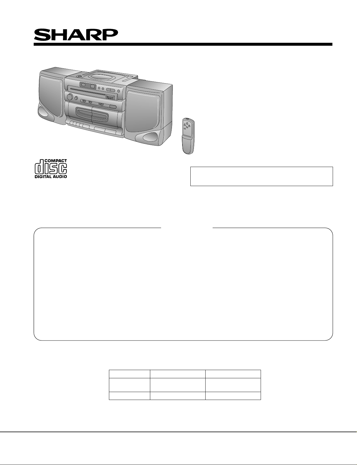
GX-CD30/30C/130/130C
SERVICE MANUAL
GX-CD30
GX-CD30C
GX-CD130
No. S3607GX-CD130
Illustration: GX-CD130
• In the interests of user-safety the set should be restored to its
original condition and only parts identical to those specified
should be used.
GX-CD130C
CONTENTS
IMPORTANT SERVICE NOTES (FOR GX-CD30/130 ONLY) .......................................................................................... 2
SPECIFICATIONS ............................................................................................................................................................. 2
NAMES OF PARTS ........................................................................................................................................................... 3
DISASSEMBLY.................................................................................................................................................................. 4
REMOVING AND REINSTALLING THE MAIN PARTS..................................................................................................... 6
ADJUSTMENT ................................................................................................................................................................... 8
TROUBLESHOOTING (CD SECTION) ........................................................................................................................... 10
NOTES ON SCHEMATIC DIAGRAM .............................................................................................................................. 13
TYPES OF TRANSISTOR ............................................................................................................................................... 13
BLOCK DIAGRAM ........................................................................................................................................................... 14
SCHEMATIC DIAGRAM / WIRING SIDE OF P.W.BOARD............................................................................................. 18
WAVEFORMS OF CD CIRCUIT...................................................................................................................................... 27
FUNCTION TABLE OF IC................................................................................................................................................ 28
PARTS GUIDE/EXPLODED VIEW
PACKING OF THE SET (FOR GX-CD30/130 ONLY)
Page
DIFFERENCE BETWEEN GX-CD30/30C AND GX-CD130/130C
GX-CD30/30C
REMOTE None Used
CONTROL
X-BASS None Used
GX-CD130/130C
SHARP CORPORATION
SHARP ELECTRONICS CORPORATION
Service Headquarters: Sharp Plaza, Mahwah, New Jersey 07430-2135
Page 2
GX-CD30/30C/130/130C
FOR A COMPLETE DESCRIPTION OF THE OPERATION OF THIS UNIT, PLEASE REFER
TO THE OPERATION MANUAL.
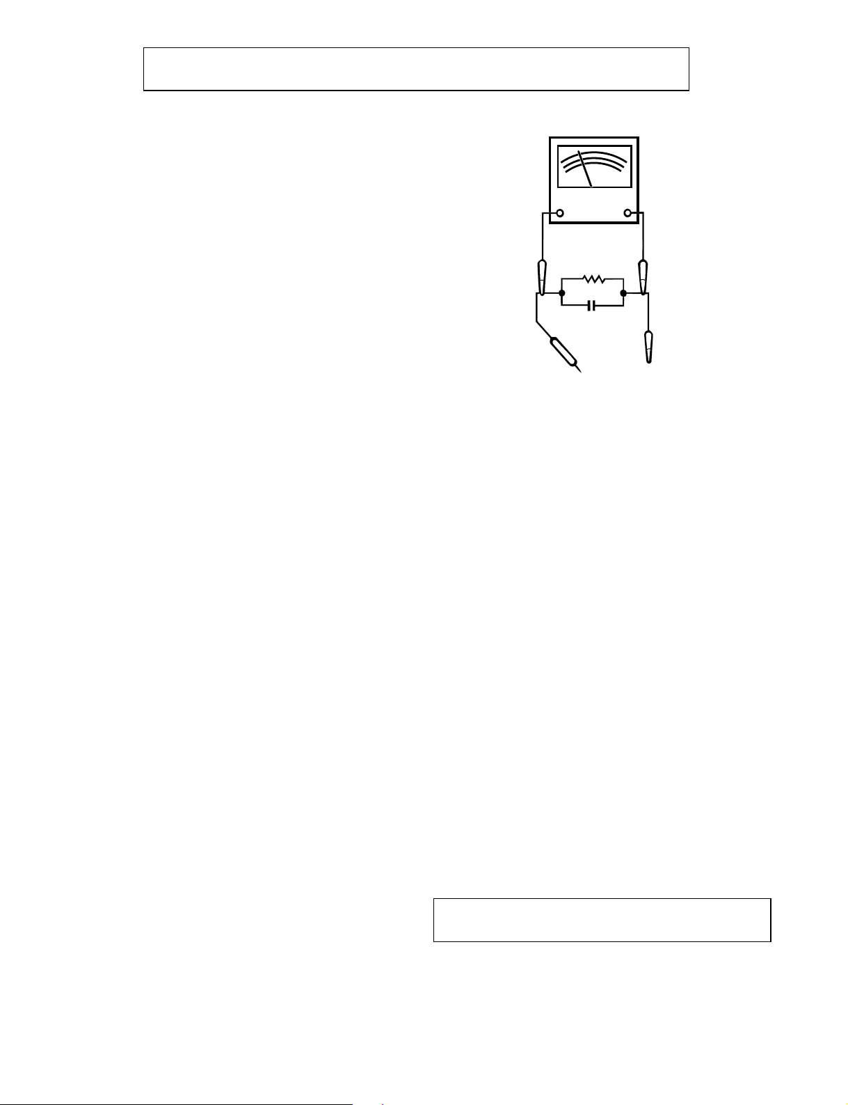
IMPORTANT SERVICE NOTES (FOR GX-CD30/130 ONLY)
BEFORE RETURNING THE AUDIO PRODUCT
(Fire & Shock Hazard)
Before returning the audio product to the user, perform the
following safety checks.
1. Inspect all lead dress to make certain that leads are not
pinched or that hardware is not lodged between the chassis
and other metal parts in the audio product.
2. Inspect all protective devices such as insulating materials,
cabinet, terminal board, adjustment and compartment
covers or shields, mechanical insulators etc.
3. To be sure that no shock hazard exists, check for leakage
current in the following manner.
* Plug the AC line cord directly into a 120 volt AC outlet.
* Using two clip leads, connect a 1.5k ohm, 10 watt resistor
paralleled by a 0.15µF capacitor in series with all exposed
metal cabinet parts and a known earth ground, such as
conduit or electrical ground connected to earth ground.
* Use a VTVM or VOM with 1000 ohm per volt, or higher,
sensitivity to measure the AC voltage drop across the
resistor (See diagram).
* Connect the resistor connection to all exposed metal parts
having a return path to the chassis (antenna, metal cabinet,
screw heads, knobs and control shafts, escutcheon, etc.)
and measure the AC voltage drop across the resistor.
VTVM
AC SCALE
1.5k ohms
10W
0.15 µ F
TO EXPOSED
METAL PARTS
All check must be repeated with the AC line cord plug connection
reversed.
Any reading of 0.3 volt RMS (this corresponds to 0.2 milliamp.
AC.) or more is excessive and indicates a potential shock
hazard which must be corrected before returning the audio
product to the owner.
TEST PROBE
CONNECT TO
KNOWN EARTH
GROUND
SPECIFICATIONS
●
General
Power source: AC 120V, 60 Hz
DC 12 V [ "D" size (UM/SUM-1, R20
or HP-2) battery x 8]
Power consumption: 25 W
Output power: FTC; 2.5 W minimum RMS per
(30/130) channel into 6 ohms from 100 Hz to
20 kHz with no more than 10 % total
harmonic distortion.
RMS; 3.5 W per channel at 1 kHz,
10 % total harmonic distortion.
(AC operation)
Output power: RMS; 7 W (3.5 W + 3.5 W)
(30C/130C) (AC operation, 10 % T.H.D.)
Output terminal: Headphones; 16 - 50 ohms
(recommended; 32 ohms)
Dimensions: Width; 12" (304 mm)
Height; 9-1/4" (234 mm)
Depth; 8-9/16" (216 mm)
Weight: 7.1 Ibs. (3.2 kg) without batteries
● Radio
Frequency range: FM; 87.6 - 108 MHz
AM; 530 - 1,702 kHz
● Tape recorder
Frequency response: 50 - 14,000 Hz (Normal tape)
Signal/noise ratio: 50 dB (TAPE 1, recording / playback)
55 dB (TAPE 2, playback)
Wow and flitter: 0.25 % (WRMS)
Motor: DC 12 V electric governor
Bias system: AC bias
Erase system: AC erase
● Compact disc player
Disc: Compact disc
Signal readout: Non-contact, 3-beam semi-
conductor laser pickup
Audio channels: 2
Quantization: 16-bit linear
Filter: 4-tims oversampling digital filter
D/A converter: 1-bit D/A converter
Wow and flutter: Unmeasurable
(less than 0.001% W. peak)
● Speaker
Type: 2-way bass-reflex type
Speakers: 4" (10 cm) woofer x 2
Tweeter x 2
Maximum input power: 5 W
Impedance: 6 ohms
Dimensions: Width; 7-5/16" (185 mm)
Height; 8-11/16" (220 mm)
Depth; 5-15/16" (150 mm)
Weight: 2.2 Ibs. (1.0 kg) /each
Specifications for this model are subject to change without
prior notice.
– 2 –
Page 3
NAMES OF PARTS
25˚
25˚
H Main Unit
1. CD Play Indicator:
2. CD Repeat Indicator:
3. CD Track Number Indicator
4. CD Eject Button:
5. Remote Control Sensor (GX-CD130/130C ONLY)
6. CD compartment
7. (CD) Track Down/Review Button:
8. (CD) Track Up/Cue Button:
9. (CD) Stop Button:
10. (CD) Play/Repeat Button:
11. (CD) Pause Button:
12. Tuning Control
13. Power/Function/Band Selector Switch
14. Beat Cancel Switch
15. X-Bass Switch (GX-CD130/130C ONLY)
16. Tone Control
17. Volume Control
18. Tweeter
19. Woofer
20. Bass Reflex Port
21. (TAPE1) Cassette Compartment
22. (TAPE1) Record Button:
23. (TAPE1) Play Button:
24. (TAPE1) Rewind Button:
25. (TAPE1) Fast Forward Button:
26. (TAPE1) Stop Eject Button:
27. (TAPE2) Play Button:
28. (TAPE2) Stop Eject Button:
29. (TAPE2) Cassette Compartment
30. Speaker Terminals
31. FM Telescopic Rod Aerial
32. Speaker Wire
33. Speaker Release Lever
34. Battery Compartment
35. Headphones Socket
36. AC Power Input Socket
H Remote Control (GX-CD130/130C ONLY)
1. Remote Control Transmitter LED
2. (CD) Play/Repeat Button:
3. (CD) Track Down /Review Button:
4. (CD) Pause Button:
5. (CD) Track Up/Cue Button:
6. (CD) Stop Button:
00
0
00
RR
R
RR
77
7
77
5 5
3 3
5 /
3
5 5
3 3
44
22
4 /
2
44
22
HH
H
HH
0R0R
0R
0R0R
66
6
66
II
I
II
00
0
00
33
3
33
22
2
22
H H
7 7
H /
7
H H
7 7
00
0
00
H H
7 7
H /
7
H H
7 7
0R0R
0R
0R0R
5 5
3 3
5 /
3
5 5
3 3
66
6
66
4 4
22
4 /
2
4 4
22
HH
H
HH
14
15
16
17
18
19
20
GX-CD30/30C/130/130C
3
1
2
4 5 6 7 8 9 1011 12 13
21 22 23 24 25 26 27 28 29
32
30 31 32
33 33363534
1
2
3
4
18
19
20
5
6
Notes concerning use:
• Periodically clean the transmitter LED on the remote control
and the sensor on the main unit with a soft cloth.
• Exposing the sensor on the main unit to strong light may
interfere with operation. Change the lighting or the direction
of the unit.
• Keep the remote control away from moisture, excessive
heat, shock, and vibrations.
8" - 20' (0.2 - 6 m)
– 3 –
Page 4
GX-CD30/30C/130/130C
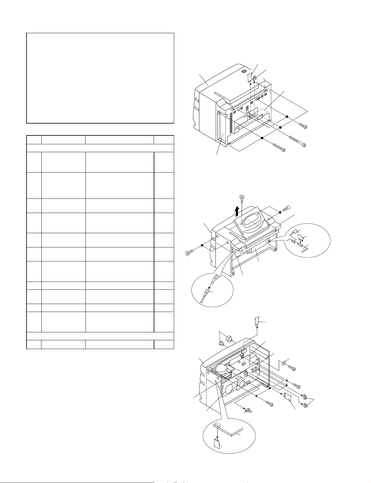
DISASSEMBLY
Caution on Disassembly
Follow the below-mentioned notes when disassembling the
unit and reassembling it, to keep it safe and ensure excellent
performance:
1. Take cassette tape and compact disc out of the unit.
2. Be sure to remove the power supply plug from the wall
outlet before starting to disassemble the unit.
3. Take off nylon bands or wire holders where they need be
removed when disassembling the unit. After servicing the
unit, be sure to rearrange the leads where they were
before disassembling.
4. Take suffcient care on static electricity of integrated
circuits and other circuits when servicing.
Front
Cabinet
( A3 ) x1
( A2 ) x1
Power PWB
( A1 ) x2
ø3 x12mm
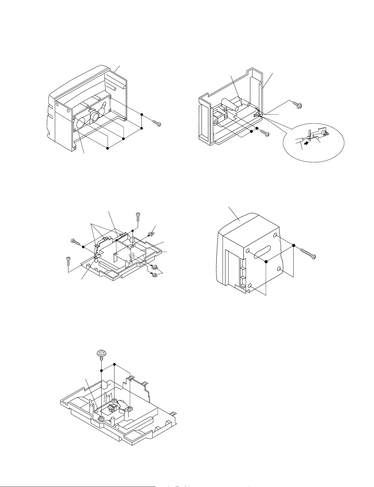
STEP REMOVAL PROCEDURE FIGURE
UNIT
1 Front Cabinet 1. Screw....................(A1) x7 4-1
2. Socket...................(A2) x1
3. Flat Cable ............. (A3) x1
2 Top Cabinet 1. Open the CD lid.
(with CD Block) 2. Screw.................... (B1) x5 4-2
3. Flat Cable ............. (B2) x2 4-2, 4-3
4. Tip.........................(B3) x1 4-2
3 Tuner PWB 1. Screw................... (C1) x3 4-3
(with Tuner Frame) 2. Flat Cable .............(C2) x1
4 Main PWB 1. Screw................... (D1) x1 4-3
2. Knob .................... (D2) x2
3. Flat Cable .............(D3) x1
5 Deck PWB 1. Screw....................(E1) x3 4-3
2. Socket...................(E2) x3
6 Tape Mechanism 1. Open the cassette holder.
2. Screw....................(F1) x6 5-1
7 Display PWB 1. Screw................... (G1) x2 5-2
(with CD control 2. Hook .................... (G2) x3
Button) 3. Flat Cable ............ (G3) x1 4-2
8 Switch PWB 1. Screw................... (H1) x1 5-2
9 CD Servo PWB 1. Screw.................... (J1) x3 5-2
2. Socket................... (J2) x3
10 CD Mechanism 1. Screw....................(K1) x3 5-3
11 Power PWB/ 1. Open the battery lid.
Terminal PWB 2. Screw.................... (L1) x4 5-4
3. Hook ..................... (L2) x1
SPEAKER
1 Front Panel 1. Screw...................(A1) x4 5-5
Front
Cabinet
( B1 ) x2
ø3 x10mm
Front
Cabinet
Rear
Cabinet
( B3 ) x1
( D2 ) x2
OPEN
Figure 4-1
( B1 ) x1
ø3 x8mm
CD Servo PWB
Tape
Mechanism
Figure 4-2
( A1 ) x4
ø3 x20mm
( B1 ) x2
ø3 x10mm
( B2 ) x1
Main PWB
Deck
PWB
( A1 ) x1
ø3 x65mm
Top Cabinet
( B2 ) x1
( G3 ) x1
CD Servo
PWB
Washer
( D1 ) x1
ø3 x10mm
( E1 ) x3
ø3 x10mm
Tuner
PWB
– 4 –
Tape
Mechanism
( C2 ) x1
( E2 ) x1
Tuner
PWB
Figure 4-3
( C1 ) x3
ø3 x10mm
( E2 ) x2
( D3 ) x1
Page 5
Tape
Power PWB
Terminal
PWB
( L1 ) x3
ø3 x10mm
( L1 ) x1
ø3 x10mm
Rear Cabinet
Driver
Push
( L2 ) x1
( A1 ) x4
ø3 x20mm
Front Panel
Mechanism
GX-CD30/30C/130/130C
Front Cabinet
( F1 ) x6
ø3 x10mm
( G1 ) x2
ø3 x10mm
( H1 ) x1
ø3 x12mm
( G2 ) x3
Switch
PWB
( K1 ) x3
ø2.6 x10mm
Figure 5-1
Display
PWB
Figure 5-2
Figure 5-4
( J1 ) x3
ø3 x10mm
( J2 ) x1
CD Servo
PWB
Top Cabinet
( J2 ) x2
Figure 5-5
CD Mechanism
Figure 5-3
– 5 –
Page 6
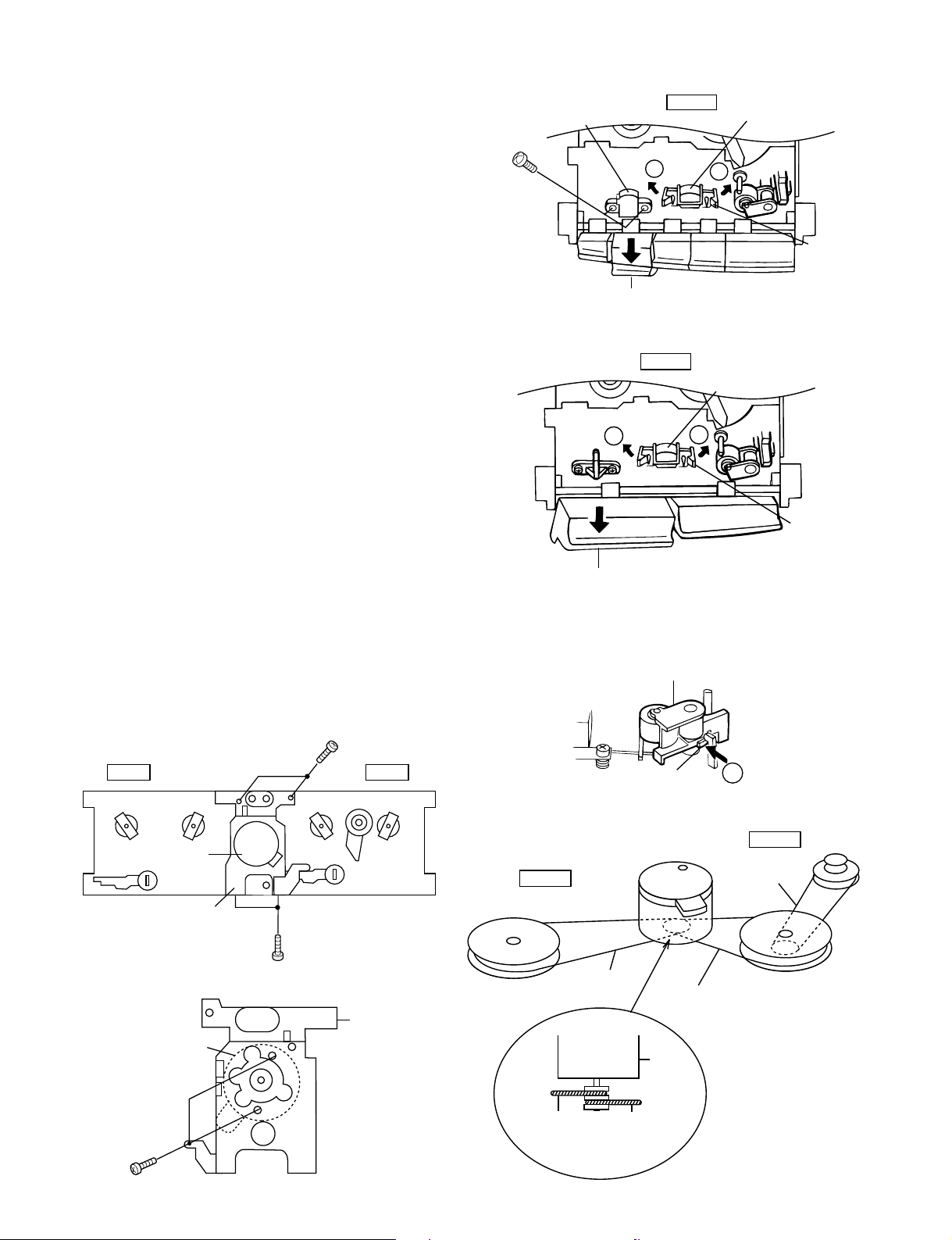
GX-CD30/30C/130/130C
Pawl
(C1)x2
Play Button
Playback Head
B
B
TAPE 2
TAPE1
Main Belt
(E1)x1
TAPE2
Main Belt
(F1)x1
Main Belt
(F1)x1
Main Belt
(E1)x1
FF/REW Belt
(E2)x1
Flywheel
Flywheel
Motor
Motor
TAPE 1
TAPE 2
REMOVING AND REINSTALLING THE MAIN PARTS
TAPE MECHANISM SECTION
Perform steps 1, 2, 3, 4, 5 and 6 of the disassembly method
to remove the tape mechanism.
How to remove the record/playback and erase
heads (TAPE 1) (See Fig. 6-1.)
1. Carefully bend the record/playback head pawls (A1) x 2
pcs., in the direction of the arrow Â, and remove the record/
playback head upwards.
2. Remove the screws (B1) x 2 pcs., to remove the erase head.
How to remove the playback head (TAPE 2)
(See Fig. 6-2.)
1. Carefully bend the playback head pawls (C1) x 2 pcs., in the
direction of the arrow È, and remove the playback head
upwards.
How to remove the pinch roller (TAPE 1/2)
(See Fig. 6-3.)
1. Carefully bend the pinch roller pawl in the direction of the
arrow Ê, and remove the pinch roller (D1) upwards.
How to remove the belt (TAPE 1) (See Fig. 6-4.)
1. Remove the main belt (E1) x 1 pc., from the motor side.
2. Remove the FF/REW belt (E2) x 1 pc.
How to remove the belt (TAPE 2) (See Fig. 6-4.)
1. Remove the tape 2 main belt (E1) x 1pc., from the motor side.
2. Remove the tape 1 main belt (F1) x 1pc., from the motor side.
( B1 ) x2
ø2 x7mm
Erase Head
Play Button
TAPE 1
A
Figure 6-1
Record/Playback
Head
A
Pawl
(A1)x2
How to remove the motor
(See Figs. 6-5 and 6-6.)
1. Remove the belt.
2. Remove the screws (G1) x 4 pcs., to remove the motor fixture.
3. Remove the screws (G2) x 2 pcs., to remove the motor.
Note:
When mounting the motor, pay attention to the motor mounting
angle.
TAPE2 TAPE1
Motor
Motor
Bracket
Motor
( G1 ) x2
ø2 x4mm
Figure 6-5
( G1 ) x2
ø2 x4mm
Motor
Bracket
Figure 6-2
Pinch Roller
(D1) x 1
Pawl
Figure 6-3
C
( G1 ) x2
ø2.6 x2mm
Figure 6-6
Figure 6-4
– 6 –
Page 7
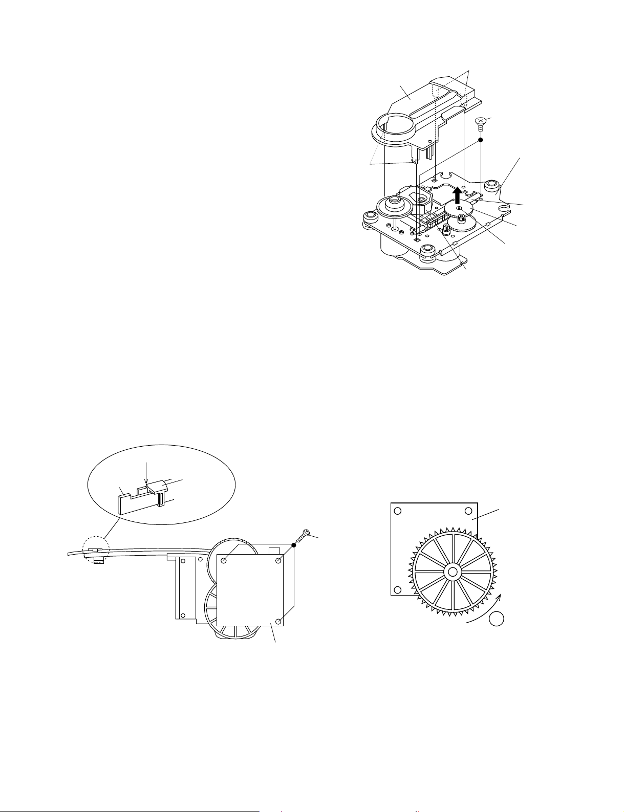
CD MECHANISM SECTION
Pickup
( F2 ) x2
ø2.6 x6mm
( F1 ) x2
CD Mechanism
CD Cover
Shaft
( F3 ) x1
Gear
( F5 ) x1
Stop Washer
( F4 ) x1
( F1 ) x2
Perform steps 1, 2, 9 and 10 of the disassembly method to
remove the CD mechanism.
How to remove the pickup (See Fig. 7-1.)
1. Remove the hooks (F1) x 4 pcs., to remove the CD cover.
2. Remove the screws (F2) x 2 pcs., to remove the shaft (F3)
x1 pc.
3. Remove the stop washer (F4) x1 pc., to remove the gear
(F5) x 1 pc.
4. Remove the pickup.
GX-CD30/30C/130/130C
Figure 7-1
FITTING OF DIAL POINTER
1. Remove the three screws, and remove the tuner PWB from the tuner frame. (See Fig. 7-2)
2. Turn fully the dial wheel in the  direction. (See Fig. 7-3)
3. Set the dial pointer as shown in Figure 7-2, and mount the tuner PWB.
"0" Point
Tuner
Frame
Dial
Pointer
( 229 )
Screw x3
Tuner PWB
(Top view)
Tuner PWB
(Bottom view)
A
Figure 7-2 Figure 7-3
– 7 –
Page 8
GX-CD30/30C/130/130C
Pin 13 of IC2 Pin 21 of IC2
D
G
S
10 kohm
TO FREQUENCY
COUNTER
FET : 2SK19 or 2SK54
ADJUSTMENT
MECHANISM SECTION
• Driving Force Check
Torque Meter
PLAY: TW-2412 Tape 1: Over 50 g
Tape 2: Over 100 g
• Torque Check
Torque Meter
Play: TW-2111 30 to 60 g.cm 30 to 60 g.cm
Fast Forward: TW-2231 80 to 135 g.cm
Rewind: TW-2231 80 to 135 g.cm
• Tape Speed
Test Tape
Nomal MTT-111 3,000 Speaker
speed ± 30 Hz terminal
Specified
TAPE SECTION
Position of each switch or control
Volume control Max
Beat cancel A
Function/Power switch Tape/Off
• Bias Oscillation Check
Beat cancel A: 82 + 10 kHz / -6 kHz
• Erase Current Check
Resistor for measurement: 1 ohm 50 ± 25 mV
Specified Value
Specified Value
Tape 1 Tape 2
Instrument
Value
B: -2 ± 2 kHz
C: +3 ± 2 kHz
Connection
(Load resistance:
6 ohms)
Specified Value
Specified Value
TUNER SECTION
fL: Low-range frequency
fH: High-range frequency
• FM IF/RF
Test Stage
IF T1
Detection T2
Band Coverage fL: L2
Tracking 88.0 MHz: L1
Specified
Value/Adjusting
Point
fH: TC2
108.0 MHz: TC1
• AM IF/RF
Test Stage
IF T3 Input: Antenna
Band Coverage fL: L4 Input: Antenna
Tracking 600 kHz: L3 Socket (Load
Specified
Value/Adjusting
Point
fH: TC4 Output: Headphones
1,400 kHz: TC3 resistance: 32 ohms)
• VCO Frequency
Adjusting Point
VR1 76 kHz ± 200 Hz Pin 13, pin 21 and
Note:
After preparing the test circuit shown in Fig. 8-1, connect the
Pin 13, Pin 21 and ground of the IC2 with the test circuit, and
measure the value. At this time, apply a standard unmodulated
signal input and adjust the VCO.
Specified
Value
Instrument
Connection
Input: Pin 1 of IC1
Output: Pin 17 of IC2
Iuput: Antenna
Output: Headphones
Socket (Load
resistance: 32 ohms)
Instrument
Connection
Output: Pin 19 of IC2
Instrument
Connection
ground of IC2
• Playback Amplifier Sensitivity Check
Specified Value
MTT-118 1.8 V ± 3 dB Speaker Terminal
(Load resistance: 6 ohms)
FM
TRACKING
Instrument ConnectionTest Tape
fH
fL
L3
AM BARANTENNA
AM TRACKING fL
Figure 8-2 ADJUSTMENT POINTS
AM TRACKING
fH
TC3
TC1
L1
FM RF
1
IC1
T1
FM IF
TC4
TC2
L2
– 8 –
L4
Figure 8-1 VCO FREQUENCY TEST CIRCUIT
AM BANDfH
fL
COVERAGE
VCO
VR1
T2
FM BANDfL
fH
FM DET
21
1
T3
19
17
IC2
AM IF
13
COVERAGE
Page 9
CD SECTION
3
Since this CD system incorporates the following automatic
adjustment function, when the pickup is replaced, it is necessary
to reajust it.
Since this CD unit does not need adjustment, the combination
of PWB and laser pickup unit is not restricted.
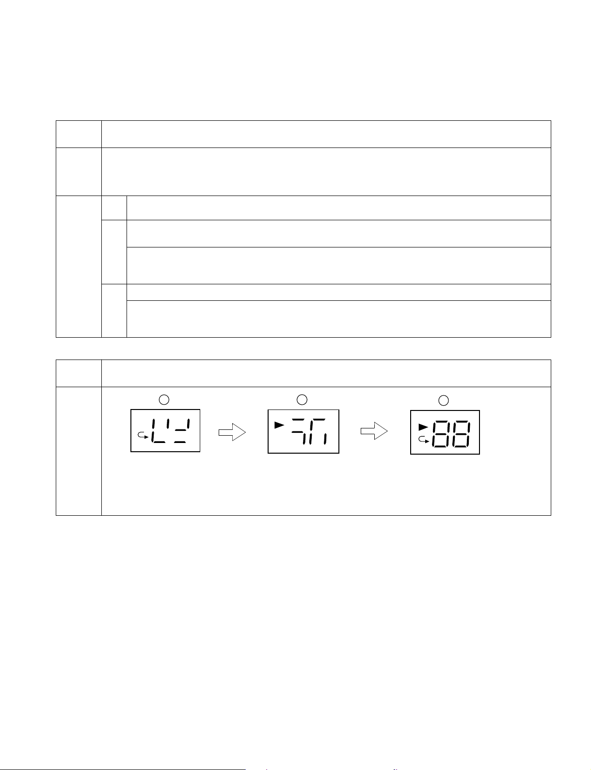
TEST MODE
GX-CD30/30C/130/130C
Start
Note
Operation
LCD MODE
Start
Display
While holding down the "STOP" button, move the FUNCTION/POWER switch to "CD".
Then, release the "STOP" button and, within 0.5 second, press the PAUSE button.
1. When the CD LID switch is in the OFF position, the unit will be able to enter the test mode.
However, playback cannot be performed in this mode.
2. You can only move the pickup.
3. The LCD display should be the same as it is for normal CD operations.
The use of the "UP/CUE" button will move the pickup to the outermost position.
1
The use of the "DOWN/REVIEW" button will move the pickup to the innermost position.
When the "PLAY" button is pressed, the laser will be lit, and when the "STOP" button is pressed, it will be
2
turned off. Playback will also start and stop when these buttons are pressed.
a. If the "PLAY" button is pressed while in the stop mode, the laser will simply be turned on at first.
b. If the laser is lit and the "PLAY" button is pressed again, playback will start from the current pickup position.
c. If the "STOP" button is pressed, playback will stop. When pressed again, the laser will be turned off.
Turning the tracking servo on or off.3
a. Each time the PAUSE button is pressed during playback, the tracking servo will be turned on or off.
(Note: If the PLAY button is pressed while in the stop mode, the tracking servo will automatically be
turned on.)
While holding down the "STOP" button, move the FUNCTION/POWER switch to "CD".
Then, release the "STOP" button and, within 0.5 second, press the PAUSE button.
1
2
1 second
* After the number ➂ has appeared in the display, each time the "UP/CUE" button is pressed, the display will switch
in the following order: ➀, ➁, and then ➂.
1 second
– 9 –
Page 10
GX-CD30/30C/130/130C
TROUBLESHOOTING (CD SECTION)
When the CD does not function
When the CD section does not operate When the objective lens of the optical pickup is dirty,this section may not operate.Clean
the objective lens,and check the playback operation.When this section does not operate even after the above step is taken,check
the following items.
Remove the cabinet and follow the troubleshooting instructions.
"Track skipping and/or no TOC(Table Of Contents) may be caused by build up of dust other foreign matter on the laser pickup lens.
Before attempting any adjustment make certain that the lens is clean. If not, clean it as mentioned below."
Turn the power off.
Gently clean the lens with a lens cleaning tissue and a small amount of isopropyl alcohol.
Do not touch the lens with the bare hand.
• The CD function will not work.
The CD operating keys don't work.
Yes
▼
Check the CD, DPS microcomputer (IC701), power supply, 4.19
MHz and 16.93 MHz clock, and reset terminal.
Yes
▼
Check the waveform of SCK, SO (DATA) and SI (COMM).
Yes
▼
See if the pick-up is in the pick-up in SW702 position.
Yes
▼
If the items mentioned above are OK, check the main
microcomputer IC701.
• The CD operating keys work.
Check the Focus - HF system.
Playback can be performed without a disc.
Yes
▼
Does the pick-up move up and down twice?
No
▼
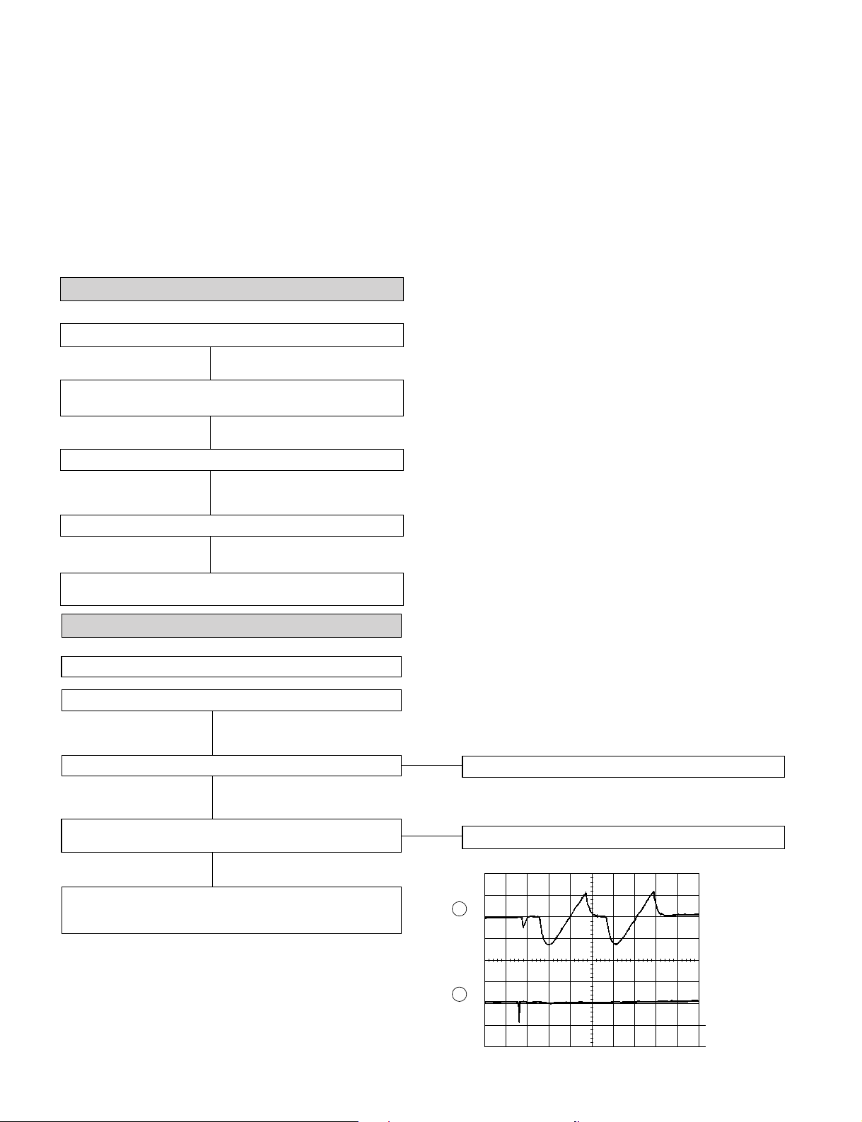
Does the output waveform of IC801(16)(FD) match that shown in
Fig. 10?
No
▼
Check the IC801(50)(CLK) line, 4MHz.
Check the microcomputer data on pins (51)(CL), (52)(DAT) and
(53)CE.
Yes
Yes
0.5s
0.50 V
IC801 16 FD
0.5s
0.50 V
IC801 15 TD
Focus search OK.
▼
Check the area around IC804-BI801/CNS801.
▼
Focus search
is performed
two times
when play
operation is
done without
disc.
– 10 –
1
2
Figure 10
Page 11

• Playback can only be performed when a disc
3
2
1
4
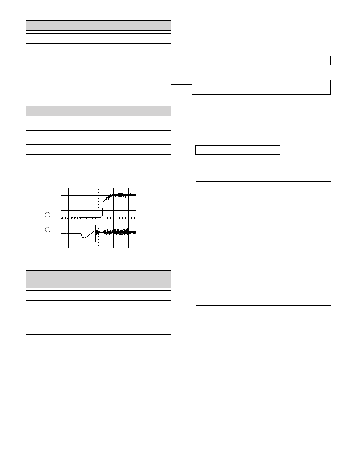
0.5s
1.00 V
IC801 16 FD
0.5s
10.0 V
IC801 12 CLV+
0.5s
10.0 V
IC801 54 DRF
0.5s
2.00 V
IC801 7 TE
is loaded.
GX-CD30/30C/130/130C
Is the Focus servo active? (Can you hear it working?)
Yes
▼
Does the DRF signal change from "L" to "H"?
Yes
▼
Is HF waveform normal (see the Fig.11-1, 2)?
Yes
▼
Check the tracking system.
HF
0.1V/DIV
0.5µsec/DIV(DC)
(When playing
back the disc)
No
No
No
Check the laser diode driver.
▼
Check the area around IC801(16) - (21) (focus servo circuit).
Yes
If the disc is not turning, the DRF
▼
should not change to "H".
Check the spin
▼
system.
Yes
Level is abnormal.
▼
Check the periphery
▼
of IC801 pins 41 and
42.
Yes
Waveform is unstable.
▼
Check the spin
▼
system.
Waveform in case
of normal playback
Figure 11-1
• Check the tracking system.
Check waveform of IC801 pin 7 (TE).
The waveform shown in Fig. 11-3
▼
appears, and no-disc state appears
soon.
Play is possible in
▼
TEST mode.
Data cannot be read.
▼
Yes
Although IL is possible,
▼
play is impossible.
Yes
5ms
1.00 V
IC801 7 TE
Tracking servo is inoperative.
▼
Yes
Normal jump is impeded, and the
▼
program top cannot be reached.
Yes
Check the VCO-PLL system.
▼
Figure 11-2
Check the periphery of IC801
Yes
4
▼
pin 8 to pin 15, and IC804 to
BI801/CNS801.
Check the periphery of
▼
IC801 pin 14.
Yes
5 ms
5.0 V
IC801 54 DRF
3
Figure 11-3
– 11 –
Page 12
GX-CD30/30C/130/130C
• Checking the spin system.
Play operation is performed without disc.
Yes
▼
The turntable rotates a little.
No
▼
The turntable fails to rotate or rotates at high speed.
• Checking the VCO-PLL system
Play operation is performed when disc exits.
Yes
▼
Although HF waveform is normal, TOC data cannot be read.
Yes
Yes
Yes
The spin driver circuit is normal.
▼
Check the periphery of IC801 pins 23 to 27, pin 39 and pin 40,
▼
IC802 pin 12 and pin 13, IC804 to BI803/CNS803.
Check PDO waveform (Fig. 12).
▼
Error
▼
Check the IC801 pins 43 and 44, IC802 pins 3, 5, 7, 9 and 10.
Stop --> Play
As VCO freque-
0.5s
1.00 V
IC802 3 PDO
0.5s
1.00 V
IC801 16 FD
ncy is locked at
4.32 M Hz,
voltage of PDO
2
rises and stabilizes.
3
Figure 12
• Although HF waveform is normal and the time
indication is normal, no sound is emitted.
Check IC802 pin 48 (EFLG).
Yes
▼
Check IC802 pins 37and 40.
Abnomal
▼
Check the periphery of IC803 (OPAMP).
No
Usually, the number of pulses of flawless disc is 100 pulses/
▼
sec or less.
– 12 –
Page 13

NOTES ON SCHEMATIC DIAGRAM
GX-CD30/30C/130/130C
• Resistor:
To differentiate the units of resistors, the symbol as K and M
are used: the symbol K means 1000 ohm and the symbol M
means 1000 kohm and the resistor without any symbol is an
ohm resistor. The resistor designated "Fusible" is a fuse type
resistor
• Capacitor:
To indicate the unit of capacitor, a symbol P is used: this
symbol P means micro-micro-farad and the unit of the capacitor
without such a symbol is microfarad. As to electrolytic capacitor,
the expression “capacitance/withstand voltage” is used.
(CH), (TH), (RH), (UJ): Temperature compensation
(ML): Mylar type
(P.P.): Polypropylene type
• The indicated voltage in each section is the one measured by
Digital Multimeter between such a section and the chassis
with no signal given.
REF. NO DESCRIPTION POSITION POSITIONREF. NO DESCRIPTION
SW201 RECODE/PLAYBACK OFF
SW351 BEAT CANCEL A
SW500 X-BASS [130/130C ONLY] OFF
SW501 POWER/FUNCTION OFF
SW605 TAPE 1 MAIN OFF
SW606 TAPE 2 MAIN OFF
SW607 TAPE1/2 SELECTOR OFF
1. Tuner
( ): AM mode
Marking except for ( ): FM mode
2. CD
( ): Play mode
Marking except for ( ): Stop state
3. Deck section
( ): Record mode
Marking except for ( ): Playback mode
Display / Control section:
( ): Active state
Marking except for ( ): CD Function mode at stop state
• Schematic diagram and Wiring Side of P.W.Board for this
model are subject to change for improvement without prior
notice.
• Parts marked with “ î ” ( ) are important for
maintaining the safety of the set. Be sure to replace these
parts with specified ones for maintaining the safety and
performance of the set.
SW702 PICKUP IN OFF
SW761 CD LID OPEN/CLOSE OFF
SW771 CD-PLAY/REPEAT OFF
SW772 CD-STOP OFF
SW773 CD-UP/CUE OFF
SW774 CD-DOWN/REVIEW OFF
SW775 CD-PAUSE OFF
FRONT
VIEW
ECB
(S)(G)(D)
(1) (2) (3)
2SC2001 K
2SD468 C
KRA102 M
KRC102 M
KTA1266 GR
KTC3199 GR
FRONT
VIEW
BCE
2SD2394 F
Figure 13 TYPES OF TRANSISTOR
– 13 –
Page 14

GX-CD30/30C/130/130C
6
5
VCC1
O
2
8
4
D
E
0
LCD771
CD LCD
RX771
REMOTE
SENSOR
31
CD LID
OPEN/CLOSE
SW761
CD
OPERATION
KEY
SW771~SW775
2
321
CFW772
321
PICKUP UNIT
LASER
DRIVER
+
X701
4.19MHz
57
60 41 44 30 33 22 23
~~
K1
SEG1
SEG4
24
27
28
31
34
35
36
COM0
COM3
IC701
IX0105AW
SYSTEM
MICROCOMPUTER
MUTE
7
RES
9
RC IN
SL–
DRF
~~ 1732 14
WRQ
19
XIN
VLC3
VDD
RESET
21
LID
SL+
SL–
XOUT
37
38
25
13
14
20
+5V
(D)
FOCUS COIL
TRACKING COIL
1
2
3
4
30
FIN2
FIN1
E
F
SL–
SL+
15
TO
16
Q805
FD
LA9
SERV
SPO
SLEO
273128
29
IC
SLD
+5V
MUTE
SYNC.IN
321
CNP603
FROM MAIN SECTION
PICKUP IN
SW702
PU-IN SW
M701
SPIN
MOTOR
M702
SLIDE
MOTOR
Figure 14 BLOCK DIAGRAM (1/4)
– 14 –
M
M
19 23 25
10
3
1
2
11
12
FOCUS/TRA
17
/SPIN/SLI
18
26
27
IC80
BA592
DRIV
Page 15

GX-CD30/30C/130/130C
FD
ASER
RIVER
+5V
805
64 62
VCC1
IC801
LA9240M
SERVO AMP.
SLD
SPO
SLEO
27 28 29
+5V
49
Q804
LDO
44
SLI
43
SLC
40
CV+
~
32
JP–
CE
DRF
DAT
CL
CLK
THLD/DEF
50 525351
54
CL, DAT, SELIAL CONTROL
CONSTANT
VOLTAGE
REGULATOR
XL801
16.93MHz
44
XOUT
EFMO
9
10
EFMIN
12
CLV+
13
CLV–
14
15
16
17
18
19
20
SERVO/SIGNAL
V/P
HFL
TES
TOFF
TGL
JP+
RES. CQCK. COIN
JP–
SQOUT. RWC. WRQ
61 58
57
1
45
XIN
IC802
LC78622E
CONTROL
56395538543353
+5V
23
6
VVDD
43
VDD
XVDD
LCHO
42
8
64
63
62
51
37
+7.4V
(CD)
46
32
11
CNP851
1
2
3
4
5
R-CH
GND (A)
L-CH
+7.4V (D)
GND (D)
TO
MAIN
SECTION
19 23 25
IC804
BA5920FP
US/TRACKING
PIN/SLIDE
DRIVER
22
+7.4V
2
5
6
7
8
13
28
Figure 15 BLOCK DIAGRAM (2/4)
– 15 –
Page 16

GX-CD30/30C/130/130C
M
E
M
G
R
S
S
ROD ANTENNA
1
FROM CD
SECTION
TO CD
SECTION
T2 PB HEAD
REC/PB
T1
ERASE
F1
B. P. F
L-CH
R-CH
SELECTOR
L-CH
HEAD
R-CH
HEAD
3
FW851
CNP603
T1/T2
SW607
1
2
3
1
MUTE
SYNC. IN
P.B
P. B
REC
FM FRONT END
RF AMP
2
3
L1
FM RF
R-CH
AUDIO GND
L-CH
CD+7.3V
POWER GND
REC/PB
SW201
C, D, E, F
P. B
REC
SW351
BEAT
CANCEL
IC1
LA1186N
MIX OSC
VCC
69
5
FM
+B
8
L2
FM OSC
P.B
REC
Q351
L351
BIAS
OSC.
23
2
1
19
7
18
7
4
L (T2)
R (T2)
L (T1)
R (T1)
T1/T2
L
R
AM BAR ANT.
POWER/
FUNCTION
SW501-A, B
L
R
L
R
Q252
T1
FM IF
L3
RADIO
CD
TAPE
21
4
15
RECORD/PLAYBACK
1224
13
9
16
REC
LA7345K
PLAYBACK AND
+B2
SW201-B
REC/PB
SW201-A
REC/PB
10.7MHz
IC2
LA1805
FM/AM
IF MPX.
IC201
AMP.
CF2
M601
TAPE
MOTOR
M
AM IF
T3
1
RF
22
REG.
23
3
MPX
OSC
24
TONE
VR532
A, B
VOLTAGE
REGULATO
Q405
+B1
F
L
A
Figure 16 BLOCK DIAGRAM (3/4)
– 16 –
Page 17

SW501-C
POWER/FUNCTION
455kHz A M
CF3
FM DET
T2
TUNER
+B
FM +B
VR1
VCO
GX-CD30/30C/130/130C
MONO
TUNER +B
2
FM-IF
LEVEL-DET.
AM-IF
GND
6
AM OSC
E
2
GE
TOR
TAPE
SW605 T1 MAIN
SW606 T2 MAIN
5
DET.
DET.
AGC
4
L4
SW500
A, B
CD130/130C
ONLY
Q404
RIPPLE
Q401
FILTER
SW501-D
POWER/
FUNCTION
20
VOLUMEX-BASS
POST
AMP.
MUTE
VR531
17
TU
DRIV.
12
A,B
STAND-BY
Q403
19 18
8
+B2
RADIO
SW501-C
POWER/
FUNCTION
CD
MUTING
Q551
Q552
DRIVER
Q554
+B1
PHASE
DET.
DECODER
9
MUTE
TUNER +B
D651~D654
RECTIFIER
15 141316 11
PILOT
DET.
VCO
10
IC501
LA4597
POWER AMP.
L
2
R
6
11
5
[ “D” size (UM/SUM-1,
R20 or HP-2) battery x 8]
TRIG.
ST.
DRIV.
FF FF
ST.
SWIT.
12
10
8
+B1
SPEAKERS
T651
POWER
TRANSFORMER
BATTERY
DC 12V
7
VCC
FF
+
–
–
+
CNP552
130C/30C
21
J551
HEADPHONES
SP3
TWEETER
L-CH
SP1
WOOFER
SP2
WOOFER
R-CH
SP4
TWEETER
SO651
130/30
AC INPUT
AC 120V
60Hz
Figure 17 BLOCK DIAGRAM (4/4)
– 17 –
Page 18

GX-CD30/30C/130/130C
A
R842
22
+B
LASER DRIVER
Q805
KTA1266GR
3V
2.2V
C848
1/50
1.8V
C840
0.33/50
C849
0.022
C839
1/50
C838
0.01
C837
10/16
C835
+B
0.1/50
DEF
REF
+
–
SL–
31 32
0.0033
C820
R826
R871
4.7K
48
NC
TBC
47
THLD
FSC
46
45
DGND
SLI
44
–
+
43
SLC
RFS–
42
C830
41
40
39
38
37
36
35
34
33
R827
220K
R810
2.2P
82K
RFSM
CV+
SLOF
HFL
TES
TOFF
TGL
JP+
SL+
JP–
220K
B
C803
0.1/50
TE
C804
0.001
R804
2.2K
R805
C807
0.1/50
R807
R809
27K
R811
3.3K
6.8K
R806
100
1K
C
C809
0.047
R802
100K
R808
12K
C805
0.033
C806
0.033
C808
0.068
R803
15K
C810
180P
D
R813
R829
1K
R812
15K
33K
R828
R839
1K
22K
E
C811
0.1
R840
22K
VREF
GND
C813
0.1
FIN2
1
FIN1
2
E
3
F
4
TB
5
TE–
6
TE
7
8
9
TH
10
TA
11
TD–
12
TD
13
JP
14
TO
15
FD
16
64 63 62
VCC1
–
REF
+
REF
–
REF
REF
REF
+
–
HIST. COMP
SHOCK;WCOMP
REF
+
–
GEN
REF
REF
+
–
FD–
17
R814
10K
61 60 59 58 57 56 55 54 53 52 51 50 49
PHI
BHI
LDS
LDO
–
+
RF
FE1
–
+
+
REF
VCR
VCR
–
+
–
+
–
+
VCR
BAL
REF
JP
FSC
REF
+
–
TO
GEN
+
–
REF
+
–
FA
FA–
19
18
R815
47K
C814
0.01
WCOMP
GEN
+
–
20
+
–
C812
330P
+
FE
REF
R816
1.5K
TGL1
THDL
THD
REF
+
–
FOF
FE–
21 22 23
R817
VCR
REF
GL
SP
AGND
82K
VCC
VR
LF2
REFI
+
–
REF
+
DEF
–
–
HFL
+
+
DRF
–
IC801
LA9240M
SERVO AMP.
VCC
+
–
REF
+
–
JP
PSTR
REF
S.Q.R
+
–
REF
+
–
SPOF
REF
SPG
SP–
SPI
252624
C816
0.001
R821
56K
10K
R820
C815
R822
0.0047
6.8K
R823
39K
R819
C817
0.47/50
1.2K
FSS
VCC2
+
–
+
–
SPO
27
R824
R830
FEBAL
FOSTA
TOSTA
2FREQ
LASER
FSTA
8/12CM
SLOF
REF
TO
SLEO
28
10K
1K
CL
CE
CLK
DAT
DRF
CLK
CE
CL
DAT
LATCH
P-ON RES
REF
JP–
JP+
RF
CV–
CV+
SLOF
SLOF
OR
SLOF
+
–
+
–
REF
SLD
29 30
C819
47/10
1/50
C818
1.2K
R825
1K
R831
C833
0.001
C845
4.7/50
C821
1/50
R833
5.6K
R832
C850
0.1
R838
33K
C834
0.033
R836
47K
R837
47K
R834
C832
1K
27P
56K
R835
C831
470
HF
0.0027
C822
220P
D802
1SS133
C851
0.022
R849
100K
F
IC801
PIN
PIN
NO.
1
2
3
4
5
6
7
8
9
10
11
12
13
14
15
G
16
17
18
19
20
21
22
23
24
25
26
27
28
29
30
31
32
VOLTAGE
2.5V
2.5V
2.5V
2.5V
2.5V
2.5V
2.5V
2.5V
2.5V
2.5V
2.5V
2.5V
2.5V
2.5V
2.5V
2.5V
2.5V
2.5V
2.5V
2.5V
2.5V
0V
2.5V
2.5V
2.5V
2.5V
2.5V
2.5V
2.5V
2.2V
2.2V
0V
VOLTAGE
NO.
0V
33
5V
34
5V
35
4.8V
36
0V
37
5V
38
0V
39
0V
40
1.5V
41
2.4V
42
2.5V
43
2.5V
44
0V
45
2.5V
46
2.5V
47
0V
48
0V
49
2.4V
50
4.1V
51
52
4.7V
0V
53
0V
54
5V
55
5V
56
2.5V
57
2.5V
58
0.9V
59
0.9V
60
2.1V
61
4.2V
62
0V
63
5V
64
H
IC802
PIN
PIN
NO.
1
2
3
4
5
6
7
8
9
10
11
12
13
14
15
16
17
18
19
20
21
22
23
24
25
26
27
28
29
30
31
32
VOLTAGE
0V
0V
1.5V
0V
2V
5V
0.3V
0V
2.5V
2.5V
0V
0V
0V
5V
0V
4.8V
5V
5V
0V
0V
2.5V
0V
5V
0V
0V
0V
0V
0V
0V
5V
2.5V
0V
VOLTAGE
NO.
0V
33
0V
34
5V
35
4.7V
36
2V
37
0V
38
39
0V
40
2V
41
4.7V
0V
5V
2.3V
2V
0V
0.1V
2.2V
0V
2.5V
0V
2.5V
0V
0V
0V
4.1V
4.1V
5V
0V
2.7V
2.4V
0V
0V
0V
P26 6 - F
FW852
TO DISPLAY
PWB
P22 4 - D
FW851
TO MAIN PWB
42
43
44
45
46
47
48
49
50
51
52
53
54
55
56
57
58
59
60
61
62
63
64
D-GND
PUIN
WRQ
SQOUT
DRF
RWC
COIN
CQCK
RES
CNP852
CNP851
12
5V
11
10
9
8
7
6
SL–
SL+
5
4
3
2
1
5
4
3
2
1
SERVO PWB-D
The numbers 1 to 12 are waveform numbers shown in page 27.
1
2
34 5
Figure 18 SCHEMATIC DIAGRAM (1/5)
CD SIGNAL
5V
DIGITAL GND
PU IN
WRQ
SQOUT
DRF
SL (–)
SL (+)
RWC
CO IN
CQCK
RES
DIGITAL GND
DIGTAL +7.4V
L-CH
AUDIO GND
R-CH
– 18 –
+B
6
Page 19

GX-CD30/30C/130/130C
+B
+B
IC802
LC78622E
SERVO/SIGNAL
CONTOL
R858
C841
680
0.047
C842
0.047
R857
27K
R856
1.2K
TR–
TR+
FO+
FO–
GND
PD
VR
LD
FO+
FO–
TR–
TR+
K
E
A
B
F
CNS801
PICKUP UNIT
CNS802
K
5
5
E
4
4
A
3
3
B
2
2
F
1
1
1
1
2
2
3
3
4
4
5
5
6
6
7
7
8
8
TR–
TR+
FO–
GND
VR
LD
1/16
LD
MON
K
E
A
B
F
C
1M
1M
LT0H30M1
2200P
2200P
FO+
PD
TR+
FO+
FO–
TR–
ACTUATOR
K
B
E
A
F
C847
0.01
DEFI
1
2
TA1
3
PDO
VVSS
4
5
ISET
VVDD
6
7
FR
VSS
8
EFMO
9
EFMIN
10
TEST2
11
CLV+
12
CLV–
13
V/P
14
HFL
15
TES
16
R860
1K
4M
16M
TST11
VCO CLOCK
OSC CONTROL
JP-
JP+
19
56 55
/RES
/CQCK
U-COM
INTERFACE
2K x 8BIT
RAM
ERROR
CORRECT
FLAG
CONTROL
SYNC-DETECT
EFM DEMODULATE
PCK
FSEQ
VDD
64
63 546253
61 60 5951585057
/CS
TEST5
TEST1
SLICE LEVEL
CONTROL
CLV
DIGITAL SERVO
SERVO
COMMAND
TOFF
TGL
COIN
CONT1
24222320 211817
RWC
SQOUT
EXTERNAL
OUTPUT
CONT2
25
WRQ
CONT3
R801
1K
C802
47/10
C801
0.01
+B
52
49
PW
FSX
SBCK
EFLG
SFSY
48
SBSY
CONT4
SUB-CODE
X-TAL
GENERATOR
4FS
DIGITAL
CONT5
EMPH
29 30272826
FILTER
C2F
31
DOUT
1BIT
DAC
DIGITAL
OUT
MUTER
MUTEL
XVSS
XOUT
XVDD
RVDD
RCHO
RVSS
LVSS
LCHO
LVDD
TEST4
32
XIN
NC
NC
TEST3
47
46
+B
+B
C890
100/10
R880
100
XL801
16.93MHz
C868
10/16
C867
10/16
45
44
43
42
41
40
39
38
37
36
35
34
33
R874
100
R873
100
R876
10K
R875
10K
BI802
5
4
3
2
1
1
2
3
4
5
6
7
8
BI801
C870
0.0022
C869
0.0022
DIGITAL GND
+B
AUDIO GND
L-CH
R-CH
C887
0.022
+B
L801
0.82µH
FOCUS/TRACKING/SPIN
3.5V
1
3.5V
2
2.5V
+B+B
C846
330/10
Q804
2SD468 C
+B
7.4V
R877
5.5V
220
R878
10/16
100
ZD801
MTZJ5.6B
+B
SERVO 7.4V
4.9V
REGULATOR
C889
CONSTANT
VOLTAGE
+B
3
2.5V
4
5
0V
6
0V
7
0V
0V
8
2.5V
9
2.5V
10
F+
3.8V
11
F–
3.2V
12
0V
13
14
6.7V
C843
100/10
SLIDE DRIVER
IC804
BA5920FP
+
–
+–
+
+
–+
–
+
+
–
C873
0.01
TR+
TR–
FO–
FO+
M701
C844
330/10
PU-IN
SP+
SP–
SL+
SL–
6
6
5
5
4
4
3
3
2
2
1
1
BI803
0V
28
+
3.5V
27
–
3.5V
26
2.5V
25
–
2.5V
24
2.5V
23
VCC
22
+
–
VCC
21
–
20
19
–
18
17
+
2.9V
16
2.9V
15
+B
7.4V
0V
7.4V
2.5V
2.7V
3.8V
3.2V
CNS803
6
5
4
3
2
1
CNP803
CD MOTOR
SPIN MOTOR
+
M
–
+
M
–
M702
SLIDE MOTOR
SW702
PICKUP IN
PWB-E
+B
NOTES ON SCHEMATIC DIAGRAM can be found on page 13.
78 9101112
Figure 19 SCHEMATIC DIAGRAM (2/5)
– 19 –
Page 20

GX-CD30/30C/130/130C
A
B
SW761
CD LID
C
D
E
OPEN/CLOSE
SWITCH PWB-A5
1
FW772
3
130/130C
ONLY
RX771
R779
30/30C
ONLY
LCD771
R776
C702
SW774
DOWN/ REVIEW
R714
C701
C705
3
2
1
R711
C704
R712
R733
R716
FW772
13
C740
R743
1
2
3
4
5
6
7
8
C741
D741
Q740
3
2
1
D740
R710
R708
R709
35
30
40
45
48
50
IC701
49
55
60
R731
R732
R722
R720
R719
R718
3233
R740
R721
164
5
R728
R723
R713
25
R724
10
R741
R726
R725
R742
DISPLAY PWB-A2
R715
3
R727
R735
FW603
1
12
X701
R734
R730
FW852
20
17
15
16
1
R729
FW603
TO MAIN PWB
CNP603
P25 10 - A
F
G
H
The numbers 1 to 12 are waveform numbers shown in page 27.
1
2
34 5
Figure 20 WIRING OF P.W.BOARD (1/4)
SW773
UP/CUE
SW772
STOP
R772
R774
R773
SW771
PLAY/REPEAT
SW775
PAUSE
– 20 –
R771
6
Page 21

M701
SPIN MOTOR
GX-CD30/30C/130/130C
-
CD MOTOR PWB-E
+
M702
SLIDE MOTOR
COLOR TABLE
BR
RD(R)
OR
YL
GR
BL
VL
GY
WH(W)
BK
PK
-
BROWN
RED
ORANGE
YELLOW
GREEN
BLUE
VIOLET
GRAY
WHITE
BLACK
PINK
SW702
PICKUP IN
CNP803
PICKUP UNIT
+
654321
CNS801
23456781
RDWHGYWHGYWHGY
WH
1 8
CNS803
7 12 10
Q805
C848
R823
C817
33
XL801
R842
R839
R840
32
35
Q804
C873
BI801
BCE
R829
C849
R819
C815
R820
R821
C816
R826
R827
C822
C830
R833
C832
R832
16
17
15
20
25
30
IC802
40
45
50
49
48
1
WH
2
GY
3
WH
4
GY
5
WH
6
BI803
15212228
R810
14
16
RD
IC804
18
178
R824
R825
C889
C844
R874
R878
R877
C818
C867
C868
CNP851
R830
C869
R875
C887
C890
BCE
L801
C843
12345
R822
C819
R831
C820
R880
6
5
4
C846
3
ZD801
R873
C870
R876
CD SERVO PWB-D
R812
C813
R813
R828
R814
C811
R815
C814
R816
C812
17
R817
20
25
32
30
35
33
40
45
48
R834
R837
R835
C831
R856
10
55
101112
5
60
CNP852
9
R857
C842
164
C841
R858
C847
R860
2345678
C807
16
15
IC801
50
C850
1
CNS802
R805
R806
C809
C806
R807
C808
R809
R811
R808
C810
10
5
60
55
49
R871
C804
C805
R804
R802
R803
C803
BI802
164
15
C801
R801
C802
C840
C845
R838
C835
C834
R836
C833
C851
C838
C839
C837
D802
C821
R849
RD
WH
GY
WH
GY
11
9
2
54321
FW851
TO MAIN PWB
P25 12 - B
112
FW852
78 9101112
Figure 21 WIRING OF P.W.BOARD (2/4)
– 21 –
Page 22

GX-CD30/30C/130/130C
W
B. P. F.
ROD
ANT.
A
B
C
D
CNW2
FM RF
C16
0.0047
FM TRACKING
TUNER PWB-B
F1
321
L1
C11
220P
C4
22P
(CH)
C9
0.0047
fHfL
FM FRONT END
RF AMP
1
3
2
1.6V
C2
0.001
TC1
R1
10
C15
0.022
LA1186N
MIX
VCC
5
0V
6.8V
VC1
IC1
OSC
9
6
R2
6.8V
6.8V
33
C5
33P
(CH)
L2
FM
OSC.
R9
22K
C10
0.022
R7
390
+B
C17
0.022
1.4V
7
48
0V
6.2V
C6
15P
(RH)
FM BAND
COVERAGE
FM IF
TC3
TC4
330K
C8
4P
(CH)
TC2
fHfL
T1
AM BAR ANT.
VC3
VC4
C14
0.022
L4
0.022
C39
1.6V
FM IF IN
1.6V
fL
fH
C36
0.022
R6
820K
AM
OSC
321
AM
TRACKING
C37
220/10
STB
CF2
C20
0.022
fH
fL
1.6V
1.6V
RF IN
21
6.1V
(6.4V)
AM
+B
AM MIX
3
(6.3V)
1.6V
AM BAND
COVERAGE
FM DET.
6V
AM IF
C21
0.022
T2
C26
22/16
T3
FM DET
AGC
4
+B
R30
VCO
1.9V
(1.6V)
1415161718192021222324
RCHAM/FM
2.5V
+B+B
C28
VCO
VCO
FW851
0.0015
13
121110
5.1V
(6.6V)
C35
1/50
1.2K
1.2V
(0V)
(1V)
0.8V
LA1805
IF MPX.
VR1
6.8K
R29
15K
MPX VCO
CK 7kKHz
IC2
FM/AM
R-CH
AUDIO GND.
L-CH
CD +7.4V
POW GND
MUTE
SYNC IN
R433
3.3K
+B
FW1
R456
10K
1
2
3
R455
10K
4
5
1
2
3
CNP603
1
2
3
4
5
6
R457
1K
H : MUTE
L : REC
R458
2.2K
R441
CD
FM AUTO
AM
TAPE
SW501-A
FUNCTION
3.3K
2.2K
R434
R442
FUNCTION
SW501-B
CD
FM AUTO
AM
TAPE
+B
+B
+B
1K
C38
0.0022
(0.4V)
AM OUT
GND
6
1.6V
CF3
R27
33K
1.5V
(1.5V)
AM
IN
7
0V
C33
1/50
2134
0.022
C24
470P
C25
C23
0.0082
3.3/50
1.7V
1.5V
(1.7V)
DET
MPX-IN
OUT
TUN
INDSTIND
8
0V
0V
C31
0.022
+B
C34
1/50
+B
FM+B
AM+B
L
R
TUN+B
6
5
TO CD SERVO PWB
CNP851
P18 3 - H
C27
3.3/50
1V
(1.3V)
FM-M/ST
LCH
9
2.5V
C32
0.022
(Ra)
R35
1.8K
TO DISPLAY PWB
FW603
P26 2 - H
C22
R26
3.9K
6.1V
0.4V
(6.4V)
AM IF
5
0.2V
(0.7V)
3
1
2
CNP1
R5
C29
10/16
VC2
R25
120
R3
47
L3
AM OSC.
E
F
G
H
TAPE2
PLAYBACK HEAD
L-CH
R-CH
TAPE1
RECORD/PLAYBACK
HEAD
L-CH
R-CH
ERASE HEAD
CNS201
1
2
3
CNS202
1
2
3
4
5
1
2
3
1
2
3
4
5
CNP201
CNP202
R201
1K (HND)
R202
1K
680P
680P
C201
C202
SW201-D
SW201-C
PRPR
C203
150P
C205
680P
C206
680P
C204
150P
R
P
R
SW201-F SW201-E
R220
27K
8.2K
R222
R231
10K
R205
150P
C211
150P
C213
R203
1K
(0V)
R204
1K
(0V)
P
R232
10K
IC201 : PLAYBACK AND
RECORD/PLAYBACK AMP.
C209
C207
330P
0V
0V
(0V)
24 23 22 21 20 19 18
123
0V
0V
(0V)
C210
C208
330P
330P
150P
C214
C212
150P
150
330P
C228
C217
0.018
C215
22/16
0.6V
0.6V
C216
22/16
C218
0.018
R206
150
470P
(0.6V)
(0.6V)
R219
27K
C219
1/50
C220
1/50
R208
R207
10K
F
CNP602
L
1
L : REC
RP
AUDIO GND
AUDIO +B
SYNC.
TAPE +B
+B
+B
+B
+B
VCC
GND
BC-A
R
2
3
L
4
R
5
6
7
8
9
10
11
R243
56K
8.2K
R221
470P
C227
R241
C239
2.2/50
3V
3V
C240
R351
C354
0.027
(ML)
(3V)
(3V)
47K
R230
R229
10K
2.2/50
10K
12K
C244
22/16
3.7V
IC201
LA7345K
10 12
11
3V
0V
(3V)
C242
0.082
680K
R238
BIAS
OSC.
Q351
R352
2SC2001 K
100K
(7.2V)
0V
0V
(1.1V)
R353
22
(3.7V)
13
(0V)
33/16
C243
0V
(0.4V)
L351
330µH
6V
0V
C356
47/10
C250
C249
100/10
100K
R264
R211
10K
6.8K
0.001
C229
C231
R223
0V
0V
T1 : 0.2V
T2 : 0.8V
(0V)
L:T1
(0V)
57
0V
0V
(0V)
T1 : 0.1V
T2 : 1.2V
R224
C232
C241
10/16
C351
560P
3V
4
3V
R214
R212
6.8K
R213
2.7K
(3V)
(3V)
2.7K
C230
0.001
47
R227
560
R225
17
896
R226
0.6V
(0.6V)
C233
22/16
0.6V
(0.6V)
C234
22/16
560
C237
0.0033
0.047
C235
16 15 14
C236
0.047
0.0033
C238
47
R228
C353
0.0039
0.001
6.8K
(0V)
6.8K
0.001
220/10
R354
47
R355
47
R250
100
SW201-A
P
+B
R254
D251
1SS133
SW201-B
R265
4.7K
R262
4.7K
D203
1SS133
R
R356
47
L : T1
D254
1SS133
3
2
1
22k
Q252
KRC102 M
NOTES ON SCHEMATIC DIAGRAM can be found on page 13.
1
2
34 5
Figure 22 SCHEMATIC DIAGRAM (3/5)
– 22 –
6
Page 23

MAIN PWB-A1
GX-CD30/30C/130/130C
D
AUTO
M
PE
SW501-A
FUNCTION
FUNCTION
SW501-B
D
UTO
AM
APE
P602
L
R
ND
L
R
+B
NC.
+B
CC
ND
10
C-A
(130/130C ONLY)
R561
2.7K
C509
0.027
TONE
VR532-A
50K (A)
TONE
VR532-B
50K (A)
C510
0.027
R562
2.7K
R461
68
FW602
1
2
3
4
5
6
7
8
9
11
1
2
3
4
5
6
7
8
9
10
11
AB
SW351
BEAT
CANCEL
C561
0.027
SW500-A
X-BASS
SW500-B
X-BASS
C562
0.027
+B
+B
+B
+B
+B
+B
R517
R518
C567
0.0027
VOLUME
C568
0.0027
D405
1SS133
CD
FM AUTO
AM
TAPE
CD: 7.3V
C565
0.1/50
R565
2.7K
R566
2.7K
C566
0.1/50
VR531-B
R579
10K
FUNCTION
SW501-C
C401
0.022
Q403
KRC102 M
312
0V
0V
VR531-A
20K (B)
20K (B)
VOLUME
+B
CD: 0V
7.7V
(8V)
ON
OFF
22K
22K
OFF
ON
+B
+B
+B
D406
1SS133
D575
1SS133
RIPPLE
FILTER
Q401
2SD468 C
7.3V
7.9V
C402
C406
330/16
R571
1K
R572
1K
KTC3199 GR
11.8V
R402
100/10
CD: 7.3V
MUTING
Q551
KTC3199 GR
0V
0V
R573
0V
R575
100K
C586
0.47/50
0V
0V
R574
0V
Q552
MUTING
R570
STAND-BY
C589
2.2/50
R401
4.7
560
VOLTAGE
REGULATOR
Q405
2SD2394 F
0V
C407
10/16
4.7K
4.7K
1K
Q554
KRA102 M
12V
0V
2
3
11.4V
2
7.9V
KRA102 M
220/25
1
11.4V
Q404
C569
1/50
C575
C570
C573
100/10
1/50
C404
1
C574
1SS133
0.01
7.9V
CD:4.2V
3
C571
0.001
100/10
D572
1SS133
D573
D574
1SS133
C588
100/25
POWER AMP.
IC501
LA4597
0V
2
1.2V
1
0V
4
1.2V
7
11.2V
3
0V
6
C572
5
0.001
11.3V
D501
1SS133
R576
1K
R403
270
D401
RD8.2JB1
R410
1.5
(1/2W)
R601
2.7
5.8V
10.3V
10.3V
5.8V
8
12V
C576
0.022
FUNCTION
SW501-D
CD
FM AUTO
AM
TAPE
+B
12
13
11
10
100/10
9
C579
0V
C580
100/10
C583
1000/10
C581
0.1
(ML)
R581
1
3.3
2
3
R582
4
3.3
C582
FW652
0.1
(ML)
C584
1000/10
+B
C57
4700
or 25V
BI651
+B
1
2
+B
+B
+B
CNS651
1
2
1
2
3
4
1
2
CNP652
CNP651
R577
120
R578
120
CNP552
SPEAKERS
0.01
0.01
0.01
0.01
RL104A
RL104A
RL104A
RL104A
D651-D658:
C651-C654:
D651
D652
C651
D653
D654
C654
31
FW651
31
FM SIGNAL
AM SIGNAL
PLAYBACK SIGNAL
RECORD SIGNAL
CD SIGNAL
J551
HEADPHONES
+
–
–
+
POWER TRANSFORMER
C652
C653
BATTERY 12V
[ “D” size (UM/SUM-1,
R20 or HP-2) battery x 8 ]
SP3
TWEETER
L-CH
SP1
WOOFER
SP2
WOOFER
R-CH
SP4
TWEETER
130C/30C
T651
AC SOCKET
AC 120V
60Hz
T.F
130/30
POWER PWB-A3
TERMINAL PWB-A4
SO651
+B
+B
–
TAPE
+
M
+B
+B
C393
0.022
MECHA GND
8
7
6
5
4
3
2
1
CNP204
8
7
6
5
4
3
2
1
CNS204
TAPE MECHANISM
M601
SW608
T1/T2
MUTE
SW605
MAIN
T1
SW606
MAIN
T2
78 9101112
Figure 23 SCHEMATIC DIAGRAM (4/5)
– 23 –
Page 24

GX-CD30/30C/130/130C
C34
123456
CNP1
T1
FM IF
C33
11 12
C32
C31
10
123
C26
R9
23
1
CF3AM IF
C15
C10
123
IC1
C20
89
7
6
5
4
3
2
1
C24
C22
C39
23456789
1
CF2
R5
R1
C16
T3
C21
R3
R25
C17
R7
C2
F1
A
B
C
TUNER PWB-B
C35
R29
R30
C38
C11C36
TC2TC1
VC3 VC4
L3
AM BAR ANTENNA
R35
VR1
ROD ANNTENA (236)
COLOR TABLE
BR
L4
(233)
TC4TC3
CNW2
RD(R)
OR
YL
GR
BL
VL
GY
WH(W)
BK
PK
BROWN
RED
ORANGE
YELLOW
GREEN
BLUE
VIOLET
GRAY
WHITE
BLACK
PINK
C27
C28
IC2
13
C25
14
15
R27
16
17
18
C23
19
20
21
T2
22
R26
23
24
R6
FM DET
C29
C37
C14
C5
R2
C9
L1
L2
C6
C8
C4
VC1 VC2
BK
D
T651
POWER TRANSFORMER
D653
C653
E
T.F
D654
F
13
FW651
BATTERT
SPRING
(249)
G
BATTERY DC 12V
["D" size (UM/SUM-1,R20 or
HP-2) battery X 8]
C652
C654
D651
12
CNP651
D652
C651
SO651
AC INPUT
AC 120V 60Hz
4321
CNP652
3
FW651
1
R577
J551
J551
HEADPHONES
R578
POWER PWB-A3
L-CH R-CH
CNP552
SPEAKERS
BATTERT
TERMINAL PWB-A4
SPRING
(204)
H
1
2
34 5
6
Figure 24 WIRING OF P.W.BOARD (3/4)
– 24 –
Page 25

GX-CD30/30C/130/130C
CNS651
FW652
FW1
VR531 VR532
VOLUME
MAXMIN
C567
R571
R572
C576
C570C569
C571
1
2
R565
A
B
C568
R566
C579
IC501
13
12
11
10
C580
9
8
7
6
C575
5
4
3
2
1
C573
R574
R575
C572
R582
C582
C581
C565
C566
C574
D501
ECB
Q552
ECB
R573
R581
D572
D573
R576
R570
Q405
C586
SW500
X-BASS
R561
R562
D575
C577
P20 6 - D
TO DISP PWB
TO DISP PWB
FW603
ONOFF
A
B
R579
123
CNP603
C584
BI651
12
SW351
BEAT CANCEL
11
FW602
R601
C583
FW652
4
SW501
R455
FUNCTION
AM FM AUTO
CDTAPE
ONOFF
POWER
1
6
R461
C401
Q401
D405
D406
CFW1
D
C
P21 9 - G
CNP851
TO CD SERVO
PWB
ECB
A
B
R458
1
R457
R441
1
R433
R434
R456
Q403
C404
Q404
123
C402
123
R402
AB
R442
5
FW851
R401
D401
1
R403
[130/130C ONLY]
TONE
HIGHLOW
R518
130/130C
ONLY
B
Q554
C407
C510
123
C509
130/130C ONLY
C561
C562
130/130C
ONLY
C588
C589
R410
R517
A
D574
C406
ECB
Q551
MAIN PWB-A1
RD
GY
FW602
RECORD/PLAYBACK
SW606
TAPE2
MAIN
(47)
HEAD
SW605
TAPE1
MAIN
BKWHPK
TAPE1
SW607
TAPE1/ 2
SELECTOR
TAPE2
PLAYBACK HEAD
(47)
WHPK
ERASE HEAD
(13)
BK
WH
BRGY
TAPE MOTOR
GY
BK
SW601
DECK PWB-C
C230
R208
R214
C231
R227
L351
C239
D203
R223
C235
IC201
C354
C241
C233
R225
R220
C236
R228
R222
C232
R224
C234
10 11
15
181920212223
16
17
C244
C237
R221
R219
C227
R230
C228
C238
R226
C242
C240
12
R264
13
C249
14
C250
R241
CNP204
R243
R250
R238
C243
R232
D251
11
10
9
8
7
CNP602
6
5
4
3
2
1
R265
C393
12345678
C218
R206
R212C210
C220
C216
R204
C212
C208
C356
3
2
1
R211
CNP201
C207
R229
R352
C209
Q351
C215
C202
C211
C219
R207
C229
B
C
E
C214
123456789
C213
24
R213
R262
R353
CNS201
PK
3
BK
2
WH
1
CNS202
PK
5
BK
4
WH
3
BK
2
WH
1
+-
CNS601
GY
8
VL
7
BL
6
GR
5
YL
4
OR
3
RD
2
BR
1
D254
Q252
R356
5
4
3
2
CNP202
1
C351
C204
R254
3
2
1
R355
C203
C353
F
E
D
C
B
A
R354
REC.
R351
P.B.
C206
C205
R205
SW201
R202
C201
R201
R203
C217
R231
78 9101112
Figure 25 WIRING OF P.W.BOARD (4/4)
– 25 –
Page 26

GX-CD30/30C/130/130C
DISPLAY PWB-A2
R771
A
LCD771
4
8
B
567
C
SEG13
SEG12
SEG11
SEG10
SEG9
SEG8
SEG7
SEG6
SEG5
SEG4
SEG3
SEG2
SEG1
SEG0
P00
P01
P02
SEG14
POWER-IN
MTCONT2
P03
P10
R735
49
50
51
TR1 LED
TR2 LED
MTCONT1
52
53
54
55
56
57
58
59
60
61
62
63
64
D
E
F
G
3.9K
R772
2.7K
R773
1.8K
R774
1.5K
123
10K
R776
+B
0.022
C702
C701
0.022
AIN7
VLC1
VLC2
COM0
COM1
SEG15
SEG16
IX0105AW
SYSTEM
MICROCOMPUTER
STB (VOL)
POWER-ON
CK (VOL)
DATA (VOL)
P11
P12
P13D0D1
4321
5
VLC3
COM2
COM3
LIDSW
REMCON
IC701
MUTE
RES
SYNC-OUT
CQCK
RWC
COIN
D2D3D4D5D6D7D8D9D10
10 11 12 13 14 15 16
9876
R720
R719
R718
R722
1K
R716
10K
MUTE
SYNC. IN
12
3
R710
10K
R711
2.7K
343536373839404142434445464748
AIN6
AIN5
SYNC-IN
TORAY2
TORAY1
SIMUKE
SQOUT
SL–
SL+
R718~
R725: 15K
R723
R725
SW774
DOWN/
REVIEW
SW773
UP/CUE
SW775
PAUSE
SW771
PLAY/
REPEAT
SW772
STOP
R709
1K
K1
K2
POWER
33
P33
P40
P32
P31
INT2 P30
VREF
AVSS
XCIN
XCOUT
VDD
VSS
XOUT
XIN
RESET
P23
PU-IN
P22
WRQ
P21
DRF
P20
SRS2
SRS1
R726 1K
R728 1K
R729 1K
R731 1K
R732 1K
R733 1K
R708
1K
R712
1K
32
31
30
29
28
27
26
25
24
23
R713
22
1K
21
20
19
18
17
R734
1K R730
R724
R721
REMOTE
SENSOR
12
R779
47
R714
10K
C704
100/10
C705
0.022
X701
4.19MHz
R727
1K
1K
+B
R741
3.3K
D740
1SS133
KRC102 M
2
R740
4.7K
RX771
3
+B
R715
15K
Q740
3
1
D741
1SS133
130/130C
ONLY
R742
1K
C741
3.3/50
R743
100K
+B
SL (–)
SL (+)
+B
C740
+B
0.01
SWITCH
PWB-A5
FW772
1
3
12
11
10
1
3
OPEN/CLOSE
PIN
VOLTAGE
NO.
0V
1
0V
2
0V
3
4
0V
5
0V
6
0V
7
3.9V
8
0V
9
5V
10
4.1V
11
4.1V
12
0V
0V
13
0V
14
0.4V
15
0.4V
16
0V
17
0V
18
0V
19
0V
20
5V
21
2.5V
22
2.5V
23
0V
24
5V
25
5V
26
0V
27
0V
28
5V
29
4.8V
30
0V
31
3.8V 0V
32
CD LID
IC701
SW761
PIN
NO.
33
34
35
36
37
38
39
40
41
42
43
44
45
46
47
48
49
50
51
52
53
54
55
56
57
58
59
60
61
62
63
64
VOLTAGE
5V
0V
0V
0V
0.4V
5V
3.1V
1.5V
2.4V
2.4V
2.4V
2.4V
2.4V
2.4V
2.4V
2.4V
2.4V
2.4V
2.4V
2.4V
2.4V
2.4V
2.4V
2.4V
2.4V
2.4V
2.4V
2.4V
2.4V
0V
0V
9
8
7
6
5
P18 3 - G
CNP852
TO CD SERVO
PWB
4
3
2
1
FW852
FW603
CNP603
P22 5 - E
H
TO MAIN PWB
NOTES ON SCHEMATIC DIAGRAM can be found on page 13.
1
2
34 5
Figure 26 SCHEMATIC DIAGRAM (5/5)
6
– 26 –
Page 27

GX-CD30/30C/130/130C
FUNCTION TABLE OF IC
IC701 RH-iX0105AWZZ (IX0105AW): System Control Microcomputer
Pin No.
1* P03 MTCONT2 Input/Output
2*-5* P10-P13 POWER-IN, Input/Output
6* D0 POWER-ON Input/Output
7 D1 MUTE Input/Output
8*-12 D2-D6 SYNC-OUT, Input/Output
13,14 D7,D8 SL+,SL- Input/Output
15*,16* D9,D10 SRS2,SRS1 Input/Output
17 P20 DRF Input/Output Used to receive 4 bits at a time.
18 P21 SQOUT Input/Output Used to receive 4 bits at a time.
19 P22 WRQ Input/Output Used to receive 4 bits at a time.
20 P23 PU-IN Input/Output Used to receive 4 bits at a time.
21 RESET Input/Output
22 XIN Input Input/output terminals for the main clock generation circuit. Used by connecting a ceramic resonator
23 XOUT Output Input/output terminals for the main clock generation circuit. Used by connecting a ceramic resonator
24 VSS — GND input terminal.
25 VDD — Positive power supply terminal.
26* XCOUT Output Input/output terminals for the sub clock generation circuit. Used by connecting a crystal oscillator
27 XCIN Input Input/output terminals for the sub clock generation circuit. Used by connecting a crystal oscillator
28 AVSS Input GND input terminal for the A-D converter.
29 VREF Input Reference voltage input terminal for the A-D converter.
30 P30 REMOCONINT2 Input Used to receive 4 bits at a time.
31 P31 TORAY1 Input Used to receive 4 bits at a time.
32 P32 TORAY2 Input Used to receive 4 bits at a time.
33 P33 Input Used to receive 4 bits at a time.
34 P40 Input Used to receive 4 bits at a time.
35-37 AIN5-AIN7 Input Used to receive 4 bits at a time.
38-40 VLC3-VLC1 Input
41-44 COM3-COM0 Output LCD common output terminals.
45-61* SEG16-SEG0 Output LCD segment output terminals.
(45*-56*)
62*-64* P00-P02 Input/Output
In this unit, the terminal with asterisk mark (*) is (open) terminal which is not connected to the outside.
Terminal
Name
Port Name Function
CK (VOL), mode.The key-on wakeup function, which can be switched on or off by the software, and a pull-up
DATA (VOL), transistor,which can be turned on or off by the software, are built in.
STB (VOL)
RES,CQCK, 1 bit. One of the D ports is assigned by register Y as a data point, to execute input or output.
COIN,REC To use the port for input, set the output latch for that bit to "1". All of the output latches on port D can
Input/
Output
Used to input or output 4 bits at a time. When the output latch is set to "1", the unit will be in the input
mode. The key-on wakeup function, which can be switched on or off by the software, and a pull-up
transistor, which can be turned on or off by the software, are built in.
Used to input or output 4 bits at a time. When the output latch is set to "1", the unit will be in the input
Each terminal can be used to input or output 1 bit at a time. The output section has a latch which holds
1 bit. One of the D ports is assigned by register Y as a data point, to execute input or output.
To use the port for input, set the output latch for that bit to "1". All of the output latches on port D can
be set to "1" using the CLD command.
Each terminal can be used to input or output 1 bit at a time. The output section has a latch which holds
be set to "1" using the CLD command.
Each terminal can be used to input or output 1 bit at a time. The output section has a latch which holds
1 bit. One of the D ports is assigned by register Y as a data point, to execute input or output.
To use the port for input, set the output latch for that bit to "1". All of the output latches on port D can
be set to "1" using the CLD command.
Each terminal can be used to input or output 1 bit at a time. The output section has a latch which holds
1 bit. One of the D ports is assigned by register Y as a data point, to execute input or output.
To use the port for input, set the output latch for that bit to "1". All of the output latches on port D can
be set to "1" using the CLD command.
Reset pulse input/output terminal. When a reset is caused by the watch dog timer, an "L" level will be
output. The output is an N channel open drain.
between the XIN and XOUT terminals. There is a built-in feedback resistor between the XIN and XOUT
terminals.
between the XIN and XOUT terminals. There is a built-in feedback resistor between the XIN and XOUT
terminals.
between the XCIN and XCOUT terminals. There is a built-in feedback resistor between the XCIN and
XCOUT terminals.
between the XCIN and XCOUT terminals. There is a built-in feedback resistor between the XCIN and
XCOUT terminals.
LCD power input terminals. To use the internal resistor, connect VLC3 to VDD (if a brightness control
is needed, connect VLC3 to VDD through a resistor). When an external power supply is used, apply
voltages as follows: 0<VLC1<VLC3<VLCD<VDD.
Used to input or output 4 bits at a time. When the output latch is set to "1", the unit will be in the input
mode. The key-on wakeup function, which can be switched on or off by the software, and a pull-up
transistor, which can be turned on or off by the software, are built in.
– 28 –
Page 28

PARTS GUIDE
GX-CD30/30C/130/130C
“HOW TO ORDER REPLACEMENT PARTS”
To have your order filled promptly and correctly, please furnish the
following information.
1. MODEL NUMBER 2. REF. No.
3. PART NO. 4. DESCRIPTION
MARK: SPARE PARTS-DELIVERY SECTION
REFERENCE
CAPACITORS
There are two types of capacitors available and they can be identified
from each other by reading their Part Numbers.
• Ceramic type capacitor;
A symblo “C” or “K” is given at the 3rd digit of its Part Number like
“VCC (or K)······J.”
• Semiconductor type capacitor:
A symblo “T” is given at the 3rd digit of its Part Number like
“VCT······J.” The capacitance error of each capacitor is indicated by
the symbol given at the 13th digit of the Part Number as follows: “J”
(±5%), “K” (±10%), “M” (±20%), “N” (±30%), “C” (±0.25 pF), “D”
(±0.5pF), “Z” (+80—20%).
Tubular type ceramic capacitor is identified by the symbol TV (TQ/
CY) of the part NO. VC00TV(TQ/CY)0000000; this TV(TQ/CY) does
not mean the lead wire.
Tubular type ceramic capacitor is identified by the symbol MF(MN) of
the part.
MODEL
GX-CD30
GX-CD30C
GX-CD130
GX-CD130C
For U.S.A. only
Contact your nearest SHARP Parts Distributor to order.
For location of SHARP Parts Distributor,
Please call Toll-Free;
1-800-BE-SHARP
RESISTORS
Unless otherwise specified, resistors are ±5%, carbon type. Tubular
type carbon film resistor ±5% is identified the symbol TV (TQ/CY)
of the part No. VRS–TV(TQ/CY)0000000; this TV(TQ/CY) does
not mean lead wire.
Tubular type carbon film resistor ±5% is identified the symbol
MF(MN) of the part No. VRD–MF(MN)0000000; this MF(MN) does
not mean lead wire.
NOTE:
Parts marked with “ ” are important for maintaining the safety of the set.
Be sure to replace parts with specified ones for maintaining the safety and performance of the set.
Page 29

GX-CD30/30C/130/130C
PART CODE
★
PRICE
RANK
DESCRIPTIONNO.
INTEGRATED CIRCUITS
IC1 VHILA1186N/-1 J AE FM Front End,LA1186N
IC2 VHILA1805//-1 J AM FM/AM IF MPX.,LA1805
IC201 VHIANT345K/-1 J AM Playback and Record/ Playback
IC501 VHILA4597//-1 J AH Power Amp.,LA4597
IC701 RH-IX0105AWZZ J BA System Microcomputer,
IC801 VHILA9240M/-1 J AV Servo Amp.,LA9240M
IC802 VHILC78622E-1 J BA Servo/Signal Control,LC78622E
IC804 VHIBA5920FP-1 J AR Focus/Tracking/Spin/Slide
Amp.,LA7345K
IX0105AW
Driver,BA5920FP
TRANSISTORS
Q252 VSKRC102M//-1 J AC Digital,NPN,KRC102 M
Q351 VS2SC2001-K-1 J AD Silicon,NPN,2SC2001 K
Q401 VS2SD468-C/-1 J AD Silicon,NPN,2SD468 C
Q403 VSKRC102M//-1 J AC Digital,NPN,KRC102 M
Q404 VSKRA102M//-1 J AC Digital,PNP,KRA102 M
Q405 VS2SD2394F/-1 J AE Silicon,NPN,2SD2394 F
Q551,552 VSKTC3199GR-1 J AB Digital,NPN,KTC3199 GR
Q554 VSKRA102M//-1 J AC Digital,PNP,KRA102 M
Q740 VSKRC102M//-1 J AC Digital,NPN,KRC102 M
Q804 VS2SD468-C/-1 J AD Silicon,NPN,2SD468 C
Q805 VSKTA1266GR-1 J AB Silicon,PNP,KTA1266 GR
DIODES
D203 VHD1SS133//-1 J AA Silicon,1SS133
D251 VHD1SS133//-1 J AA Silicon,1SS133
D254 VHD1SS133//-1 J AA Silicon,1SS133
D401 VHERD8R2JB1-1 J AB Zener,8.2V,RD8.2JB1
D405,406 VHD1SS133//-1 J AA Silicon,1SS133
D501 VHD1SS133//-1 J AA Silicon,1SS133
D572ç575 VHD1SS133//-1 J AA Silicon,1SS133
îD651ç654 VHDRL104A//-1 J AB Silicon,RL104A
D740,741 VHD1SS133//-1 J AA Silicon,1SS133
D802 VHD1SS133//-1 J AA Silicon,1SS133
ZD801 VHEMTZJ5R6B-1 J AD Zener,5.6V,MTZJ5.6B
FILTERS
CF2 92LFILT-F1342A J AD FM IF
CF3 RFILA0006AWZZ J AG AM IF
F1 92LFILTF1759A J AD FM Band Pass Filter
TRANSFORMERS
T1 RCILI0007AWZZ J AD FM IF
T2 RCILI0008AWZZ J AF FM Detection
T3 RCILI0014AWZZ J AE AM IF
îT651 RTRNP0054AWZZ J AX Power
COILS
L1 RCILR0364AFZZ J AA FM RF
L2 RCILB0020AWZZ J AA FM Oscillation
L3 RCILA0053AWZZ J AK AM Bar Antenna
L4 RCILB0051AWZZ J AE AM Oscillation
L351 VP-MK331K0000 J AB 330 µH,Choke
L801 VP-XHR82K0000 J AC 0.82 µH,Choke
VARIABLE RESISTORS
VR1 92LVRS682NBUT J AC 6.8 kohms (B),Semi-VR [VCO]
VR531 92LVR-524A J AH 20 kohms (B),Semi-VR [Volume]
VR532 92LVR-524B J AG 50 kohms (A),Semi-VR [Tone]
VARIABLE CAPACITORS
VC1-4 92LVC-1455A J AN Variable Capacitor with Trimmer
(TC1-4)
VIBRATORS
X701 RCRM-0009AWZZ J AF Ceramic,4.000 MHz
XL801 RCRM-0008AWZZ J AF Ceramic,16.93 MHz
PRICE
NO. PARTS CODE
★
RANK
DESCRIPTION
CAPACITORS
C2 VCKYMN1HB102K J AA 0.001 µF,50V
C4 VCCCPA1HH220J J AA 22 pF (CH),50V
C5 VCCCPA1HH330J J AA 33 pF (CH),50V
C6 VCCRPA1HH150J J AA 15 pF (RH),50V
C8 VCCCPA1HH4R0C J AA 4 pF (CH),50V
C9 VCTYPA1EX472M J AA 0.0047 µF,25V
C10 VCTYPA1EX223M J AA 0.022 µF,25V
C11 VCKYPA1HB221K J AA 220 pF,50V
C14 VCTYMN1EF223Z J AA 0.022 µF,25V
C15 VCTYPA1EX223M J AA 0.022 µF,25V
C16 VCTYPA1EX472M J AA 0.0047 µF,25V
C17 VCTYMN1EF223Z J AA 0.022 µF,25V
C20,21 VCTYMN1EF223Z J AA 0.022 µF,25V
C22 VCTYMN1CX222K J AA 0.0022 µF,16V
C23 VCTYPA1EX822M J AA 0.0082 µF,25V
C24 VCKYMN1HB471K J AA 470 pF,50V
C25 RC-GZA335AF1H J AB 3.3 µF,50V,Electrolytic
C26 RC-GZA226AF1C J AB 22 µF,16V,Electrolytic
C27 RC-GZA335AF1H J AB 3.3 µF,50V,Electrolytic
C28 92LCPU100V1500 J AC 0.0015 µF,100V,Polypropylene
C29 RC-GZA106AF1C J AB 10 µF,16V,Electrolytic
C31,32 VCTYPA1EX223M J AA 0.022 µF,25V
C33ç35 RC-GZA105AF1H J AB 1 µF,50V,Electrolytic
C36 VCTYPA1EX223M J AA 0.022 µF,25V
C37 RC-GZA227AF1A J AB 220 µF,10V,Electrolytic
C38,39 VCTYMN1EF223Z J AA 0.022 µF,25V
C201,202 VCKYMN1HB681K J AA 680 pF,50V
C203,204 VCKYMN1HB151K J AA 150 pF,50V
C205,206 VCKYMN1HB681K J AA 680 pF,50V
C207ç210 VCKYPA1HB331K J AA 330 pF,50V
C211,212 VCKYPA1HB151K J AA 150 pF,50V
C213,214 VCKYMN1HB151K J AA 150 pF,50V
C215,216 RC-GZA226AF1C J AB 22 µF,16V,Electrolytic
C217,218 VCTYPA1EX183J J AB 0.018 µF,25V
C219,220 RC-GZA105AF1H J AB 1 µF,50V,Electrolytic
C227,228 VCKYPA1HB471K J AA 470 pF,50V
C229,230 VCKYPA1HB102K J AA 0.001 µF,50V
C231,232 VCKYMN1HB102K J AA 0.001 µF,50V
C233,234 RC-GZA226AF1C J AB 22 µF,16V,Electrolytic
C235,236 VCTYPA1CX473K J AA 0.047 µF,16V
C237,238 VCTYMN1CX332K J AA 0.0033 µF,16V
C239,240 RC-GZA225AF1H J AB 2.2 µF,50V,Electrolytic
C241 RC-GZA106AF1C J AB 10 µF,16V,Electrolytic
C242 VCTYPA1EX823K J AB 0.082 µF,25V
C243 RC-GZA336AF1C J AB 33 µF,16V,Electrolytic
C244 RC-GZA226AF1C J AB 22 µF,16V,Electrolytic
C249 RC-GZA107AF1A J AB 100 µF,10V,Electrolytic
C250 RC-GZA227AF1A J AB 220 µF,10V,Electrolytic
C351 VCKYMN1HB561K J AA 560 pF,50V
C353 VCQPKA2AA392J J AB 0.0039 µF,100V,Polypropylene
C354 RC-QZA273AFYJ J AB 0.027 µF,50V,Mylar
C356 RC-GZA476AF1A J AB 47 µF,10V,Electrolytic
C393 VCTYMN1EF223Z J AA 0.022 µF,25V
C401 VCTYMN1EF223Z J AA 0.022 µF,25V
C402 RC-GZA107AF1A J AB 100 µF,10V,Electrolytic
C404 VCTYMN1CY103K J AA 0.01 µF,16V
C406 RC-GZA337AF1C J AC 330 µF,16V,Electrolytic
C407 RC-GZA106AF1C J AB 10 µF,16V,Electrolytic
C509,510 VCTYPA1CX273K J AA 0.027 µF,16V
C561,562 VCTYPA1CX273K J AA 0.027 µF,16V [130/130C Only]
C565,566 RC-GZA104AF1H J AB 0.1 µF,50V,Electrolytic
C567,568 VCTYMN1CX272K J AA 0.0027 µF,16V
C569,570 RC-GZA105AF1H J AB 1 µF,50V,Electrolytic
C571,572 VCKYMN1HB102K J AA 0.001 µF,50V
C573,574 RC-GZA107AF1A J AB 100 µF,10V,Electrolytic
C575 RC-GZA227AF1E J AB 220 µF,25V,Electrolytic
C576 VCKZPA1HF223Z J AA 0.022 µF,50V
C577 92LCEU20W4700M J AH 4700µF,20V
C579,580 RC-GZA107AF1A J AB 100 µF,10V,Electrolytic
C581,582 RC-QZA104AFYK J AB 0.1 µF,50V,Mylar
C583,584 RC-GZS108AF1A J AC 1000 µF,10V,Electrolytic
C586 RC-GZA474AF1H J AA 0.47 µF,50V,Electrolytic
C588 RC-GZA107AF1E J AB 100 µF,25V,Electrolytic
C589 RC-GZA225AF1H J AB 2.2 µF,50V,Electrolytic
C651ç654 VCKZPA1HF103Z J AA 0.01 µF,50V
C701,702 VCTYMN0JY223N J AA 0.022 µF,6.3V
C704 RC-EZY107AF1A J AB 100 µF,10V,Electrolytic
C705 VCTYMN0JY223N J AA 0.022 µF,6.3V
C740 VCTYMN1CY103K J AA 0.01 µF,16V
C741 RC-EZY335AF1H J AB 3.3 µF,50V,Electrolytic
– 1 –
Page 30

GX-CD30/30C/130/130C
NO. PART CODE
C801 VCTYMN1CY103N J AA 0.01 µF,16V
C802 RC-GZA476AF1A J AB 47 µF,10V,Electrolytic
C803 RC-GZA104AF1H J AB 0.1 µF,50V,Electrolytic
C804 VCKYMN1HB102K J AA 0.001 µF,50V
C805,806 VCTYPA1CX333K J AA 0.033 µF,16V
C807 RC-GZA104AF1H J AB 0.1 µF,50V,Electrolytic
C808 VCTYPA1CX683K J AA 0.068 µF,16V
C809 VCTYPA1CX473K J AA 0.047 µF,16V
C810 VCKYMN1HB181K J AA 180 pF,50V
C811 VCTYPA1CX104K J AB 0.1 µF,16V
C812 VCKYMN1HB331K J AA 330 pF,50V
C813 VCTYPA1CX104K J AB 0.1 µF,16V
C814 VCTYMN1CY103K J AA 0.01 µF,16V
C815 VCTYMN1CX472K J AA 0.0047 µF,16V
C816 VCKYMN1HB102K J AA 0.001 µF,50V
C817 RC-GZA474AF1H J AA 0.47 µF,50V,Electrolytic
C818 RC-GZA105AF1H J AB 1 µF,50V,Electrolytic
C819 RC-GZA476AF1A J AB 47 µF,10V,Electrolytic
C820 VCTYMN1CX332K J AA 0.0033 µF,16V
C821 RC-GZA105AF1H J AB 1 µF,50V,Electrolytic
C822 VCKYMN1HB221K J AA 220 pF,50V
C830 VCCSMN1HL2R2C J AB 2.2 pF,50V
C831 VCTYMN1CX272K J AA 0.0027 µF,16V
C832 VCCSMN1HL270J J AA 27 pF,50V
C833 VCKYMN1HB102K J AA 0.001 µF,50V
C834 VCTYPA1CX333K J AA 0.033 µF,16V
C835 RC-GZA104AF1H J AB 0.1 µF,50V,Electrolytic
C837 RC-GZA106AF1C J AB 10 µF,16V,Electrolytic
C838 VCTYMN1CY103K J AA 0.01 µF,16V
C839 RC-GZA105AF1H J AB 1 µF,50V,Electrolytic
C840 RC-GZA334AF1H J AA 0.33 µF,50V,Electrolytic
C841,842 VCTYPA1CX473K J AA 0.047 µF,16V
C843 RC-GZA107AF1A J AB 100 µF,10V,Electrolytic
C844 RC-GZA337AF1A J AB 330 µF,10V,Electrolytic
C845 RC-GZA475AF1H J AB 4.7 µF,50V,Electrolytic
C846 RC-GZA337AF1A J AB 330 µF,10V,Electrolytic
C847 VCTYMN1CY103K J AA 0.01 µF,16V
C848 RC-GZA105AF1H J AB 1 µF,50V,Electrolytic
C849 VCTYMN1EF223Z J AA 0.022 µF,25V
C850 VCTYPA1EF104Z J AA 0.1 µF,25V
C851 VCTYMN1EF223Z J AA 0.022 µF,25V
C867,868 RC-GZA106AF1C J AB 10 µF,16V,Electrolytic
C869,870 VCTYMN1CX222K J AA 0.0022 µF,16V
C873 VCTYMN1CY103K J AA 0.01 µF,16V
C887 VCTYMN1EF223Z J AA 0.022 µF,25V
C889 RC-GZA106AF1C J AB 10 µF,16V,Electrolytic
C890 RC-GZA107AF1A J AB 100 µF,10V,Electrolytic
★
PRICE
RANK
DESCRIPTION
RESISTORS
R1 VRD-ST2EE100J J AA 10 ohm,1/4W
R2 VRD-MN2BD330J J AA 33 ohms,1/8W
R3 VRD-MN2BD470J J AA 47 ohms,1/8W
R5 VRD-ST2EE334J J AA 330 kohms,1/4W
R6 VRD-ST2EE824J J AA 820 kohms,1/4W
R7 VRD-ST2EE391J J AA 390 ohms,1/4W
R9 VRD-MN2BD223J J AA 22 kohms,1/8W
R25 VRD-ST2EE121J J AA 120 ohms,1/4W
R26 VRD-MN2BD392J J AA 3.9 kohms,1/8W
R27 VRD-MN2BD333J J AA 33 kohms,1/8W
R29 VRD-MN2BD153J J AA 15 kohms,1/8W
R30 VRD-MN2BD122J J AA 1.2 kohms,1/8W
R35 VRD-ST2EE182J J A A 1.8 kohms,1/4W
R201 VRD-ST2CD102J J AA 1 kohm,1/6W
R202ç204 VRD-MN2BD102J J AA 1 kohm,1/8W
R205 VRD-MN2BD151J J AA 150 ohms,1/8W
R206 VRD-ST2CD151J J AA 150 ohms,1/6W
R207,208 VRD-MN2BD103J J AA 10 kohm,1/8W
R211,212 VRD-MN2BD682J J AA 6.8 kohms,1/8W
R213,214 VRD-MN2BD272J J AA 2.7 kohms,1/8W
R219,220 VRD-MN2BD273J J AA 27 kohms,1/8W
R221,222 VRD-MN2BD822J J AA 8.2 kohms,1/8W
R223,224 VRD-MN2BD682J J AA 6.8 kohms,1/8W
R225,226 VRD-MN2BD561J J AA 560 ohms,1/8W
R227,228 VRD-MN2BD470J J AA 47 ohms,1/8W
R229,230 VRD-MN2BD103J J AA 10 kohm,1/8W
R231,232 VRD-ST2EE103J J AA 10 kohm,1/4W
R238 VRD-MN2BD684J J AA 680 kohms,1/8W
R241 VRD-MN2BD123J J AA 12 kohms,1/8W
R243 VRD-MN2BD563J J AA 56 kohms,1/8W
R250 VRD-ST2EE101J J AA 100 ohm,1/4W
VRD-MN2BD000C J AA 0 ohm,Jumper,ø1.4×3.5mm,Ivory
PRICE
NO.
R254 VRD-MN2BD223J J AA 22 kohms,1/8W
R262 VRD-MN2BD472J J AA 4.7 kohms,1/8W
R264 VRD-MN2BD104J J AA 100 kohm,1/8W
R265 VRD-MN2BD472J J AA 4.7 kohms,1/8W
R351 VRD-MN2BD473J J AA 47 kohms,1/8W
R352 VRD-MN2BD104J J AA 100 kohm,1/8W
R353 VRD-MN2BD220J J AA 22 ohms,1/8W
R354ç356 VRD-ST2EE470J J AA 47 ohms,1/4W
R401 VRD-ST2EE4R7J J AA 4.7 ohms,1/4W
R402 VRD-MN2BD561J J AA 560 ohms,1/8W
R403 VRD-ST2EE271J J AA 270 ohms,1/4W
R410 VRD-RT2HD1R5J J AB 1.5 ohms,1/2W
R433,434 VRD-ST2EE332J J AA 3.3 kohms,1/4W
R441,442 VRD-MN2BD222J J AA 2.2 kohms,1/8W
R455,456 VRD-MN2BD103J J AA 10 kohm,1/8W
R457,458 VRD-MN2BD102J J AA 1 kohm,1/8W
R461 VRD-ST2EE680J J AA 68 ohms,1/4W
R517,518 VRD-MN2BD223J J AA 22 kohms,1/8W [130/130C Only]
R561,562 VRD-ST2EE272J J AA 2.7 kohms,1/4W
R565,566 VRD-MN2BD272J J AA 2.7 kohms,1/8W
R570ç572 VRD-MN2BD102J J AA 1 kohm,1/8W
R573,574 VRD-MN2BD472J J AA 4.7 kohms,1/8W
R575 VRD-MN2BD104J J AA 100 kohm,1/8W
R576 VRD-MN2BD102J J AA 1 kohm,1/8W
R577,578 VRD-ST2EE121J J AA 120 ohms,1/4W
R579 VRD-MN2BD103J J AA 10 kohm,1/8W
R581,582 VRD-ST2EE3R3J J AA 3.3 ohms,1/4W
R601 VRD-ST2EE2R7J J AA 2.7 ohms,1/4W
R708,709 VRD-MN2BD102J J AA 1 kohm,1/8W
R710 VRD-MN2BD103J J AA 10 kohm,1/8W
R711 VRD-MN2BD272J J AA 2.7 kohms,1/8W
R712 VRD-MN2BD102J J AA 1 kohm,1/8W [130/130C Only]
R713 VRD-MN2BD102J J AA 1 kohm,1/8W
R714 VRD-MN2BD103J J AA 10 kohm,1/8W
R715 VRD-MN2BD153J J AA 15 kohms,1/8W
R716 VRD-MN2BD103J J AA 10 kohm,1/8W
R718ç720 VRD-ST2EE153J J AA 15 kohms,1/4W
R721 VRD-MN2BD153J J AA 15 kohms,1/8W
R722,723 VRD-ST2EE153J J AA 15 kohms,1/4W
R724 VRD-MN2BD153J J AA 15 kohms,1/8W
R725 VRD-ST2EE153J J AA 15 kohms,1/4W
R726ç735 VRD-MN2BD102J J AA 1 kohm,1/8W
R740 VRD-MN2BD472J J AA 4.7 kohms,1/8W
R741 VRD-MN2BD332J J AA 3.3 kohms,1/8W
R742 VRD-MN2BD102J J AA 1 kohm,1/8W
R743 VRD-MN2BD104J J AA 100 kohm,1/8W
R771 VRD-MN2BD392J J AA 3.9 kohms,1/8W
R772 VRD-MN2BD272J J AA 2.7 kohms,1/8W
R773 VRD-MN2BD182J J AA 1.8 kohms,1/8W
R774 VRD-MN2BD152J J AA 1.5 kohms,1/8W
R776 VRD-MN2BD103J J AA 10 kohm,1/8W
R779 VRD-MN2BD470J J AA 47 ohms,1/8W [130/130C Only]
R801 VRD-MN2BD102J J AA 1 kohm,1/8W
R802 VRD-MN2BD104J J AA 100 kohm,1/8W
R803 VRD-MN2BD153J J AA 15 kohms,1/8W
R804 VRD-MN2BD222J J AA 2.2 kohms,1/8W
R805 VRD-MN2BD682J J AA 6.8 kohms,1/8W
R806 VRD-MN2BD101J J AA 100 ohm,1/8W
R807 VRD-MN2BD102J J AA 1 kohm,1/8W
R808 VRD-MN2BD123J J AA 12 kohms,1/8W
R809 VRD-MN2BD273J J AA 27 kohms,1/8W
R810 VRD-MN2BD823J J AA 82 kohms,1/8W
R811 VRD-MN2BD332J J AA 3.3 kohms,1/8W
R812 VRD-MN2BD153J J AA 15 kohms,1/8W
R813 VRD-MN2BD333J J AA 33 kohms,1/8W
R814 VRD-MN2BD103J J AA 10 kohm,1/8W
R815 VRD-MN2BD473J J AA 47 kohms,1/8W
R816 VRD-MN2BD152J J AA 1.5 kohms,1/8W
R817 VRD-MN2BD823J J AA 82 kohms,1/8W
R819 VRD-MN2BD393J J AA 39 kohms,1/8W
R820 VRD-MN2BD103J J AA 10 kohm,1/8W
R821 VRD-MN2BD563J J AA 56 kohms,1/8W
R822 VRD-MN2BD682J J AA 6.8 kohms,1/8W
R823 VRD-MN2BD122J J AA 1.2 kohms,1/8W
R824 VRD-MN2BD103J J AA 10 kohm,1/8W
R825 VRD-MN2BD122J J AA 1.2 kohms,1/8W
R826,827 VRD-MN2BD224J J AA 220 kohms,1/8W
R828,829 VRD-ST2EE102J J AA 1 kohm,1/4W
R830 VRD-ST2EE102J J AA 1 kohm,1/4W
R831 VRD-MN2BD102J J AA 1 kohm,1/8W
R832 VRD-MN2BD563J J AA 56 kohms,1/8W
R833 VRD-MN2BD562J J AA 5.6 kohms,1/8W
★
RANK
DESCRIPTIONPARTS CODE
– 2 –
Page 31

GX-CD30/30C/130/130C
PRICE
PART CODE
R834 VRD-MN2BD102J J AA 1 kohm,1/8W
R835 VRD-MN2BD471J J AA 470 ohms,1/8W
R836,837 VRD-MN2BD473J J AA 47 kohms,1/8W
R838 VRD-MN2BD333J J AA 33 kohms,1/8W
R839,840 VRD-MN2BD223J J AA 22 kohms,1/8W
R842 VRD-ST2EE220J J AA 22 ohms,1/4W
R849 VRD-MN2BD104J J AA 100 kohm,1/8W
R856 VRD-MN2BD122J J AA 1.2 kohms,1/8W
R857 VRD-MN2BD273J J AA 27 kohms,1/8W
R858 VRD-MN2BD681J J AA 680 ohms,1/8W
R860 VRD-MN2BD102J J AA 1 kohm,1/8W
R871 VRD-MN2BD472J J AA 4.7 kohms,1/8W
R873,874 VRD-MN2BD101J J AA 100 ohm,1/8W
R875,876 VRD-MN2BD103J J AA 10 kohm,1/8W
R877 VRD-ST2EE221J J AA 220 ohms,1/4W
R878 VRD-MN2BD101J J AA 100 ohm,1/8W
R880 VRD-MN2BD101J J AA 100 ohm,1/8W
★
RANK
DESCRIPTIONNO.
OTHER CIRCUITRY PARTS
BI651/CNS651 QCNWN0602AWZZ J AG Connector Ass’y,2-2Pin
BI801/CNS801 QCNWN0605AWZZ J AL Connector Ass’y,8-8Pin
BI802/CNS802 QCNWN0606AWZZ J AH Connector Ass’y,5-5Pin
BI803/CNS803 QCNWN0607AWZZ J AH Connector Ass’y,6-6Pin
CNP1 92LCONE6P52287 J AC Plug,6Pin
CNP201 92LCONE3P53253 J AB Plug,3Pin
CNP202 92LCONE5P53253 J AB Plug,5Pin
CNP204 QCNCW027HAWZZ J AC Plug,8Pin
CNP552 QTANA0404AWZZ J AF Terminal,Ext.Speaker
CNP602 QCNCW012LAWZZ J AE Plug,11Pin
CNP603 92LCONE3P52287 J AC Plug,3Pin
CNP651 QCNCM742BAFZZ J AA Plug,2Pin
CNP652 92LCONE4P52287 J AC Plug,4Pin
CNP803 QCNCM932FAFZZ J AC Plug,6Pin
CNP851 QCNCW026EAWZZ J AE Plug,5Pin
CNP852 QCNCW026MAWZZ J AG Plug,12Pin
CNS201 QCNWN0595AWZZ J AH Connector Ass’y,3Pin
CNS202 QCNWN0596AWZZ J AL Connector Ass’y,5Pin
CNS204 QCNWN0600AWZZ J AH Connector Ass’y,8Pin
CNS653 QCNWN0487AWZZ J AB Connector Ass’y,1Pin
CNW2 QCNWN0716AWZZ J AD Tip with Lead
FW1 QCNWN0687AWZZ J AE Flat Cable,6Pin
FW602 QCNWN0601AWZZ J AG Flat Cable,11Pin
FW603 QCNWN0717AWZZ J AD Flat Cable,2Pin
FW651 QCNWN0594AWZZ J AD Flat Cable,2Pin
FW652 QCNWN0718AWZZ J AD Flat Cable,4Pin
FW772 QCNWN0603AWZZ J AC Flat Cable,2Pin
FW851 QCNWN0689AWZZ J AE Flat Cable,5Pin
FW852 QCNWN0604AWZZ J AH Flat Cable,12Pin
J551 QJAKM0004AWZZ J AK Jack,Headphones
LCD771 RV-LX0018AWZZ J AQ LCD
M601 92LMTR1746AASY J AP Motor with Pulley [Tape]
M701 92LMTR1906CASY J AS Motor with Chassis [Spin]
M702 92LMTR1854BASY J AP Motor with Gear [Slide]
RX771 VHLSPS4201C-1 J AN Remote Sensor,LSPS4201C
îSO651 QSOCA0201AWZZ J AL Socket,AC Power Supply Input
îSO651 QSOCA0203AWZZ J AL Socket,AC Power Supply Input
SP1,2 VSP0010PBR26A J AP Woofer
SP3,4 RALMB0101AFZZ J AB Tweeter
SW201 QSW-S0018AWZZ J AG Switch,Slide Type [Record/
SW351 QSW-S0024AWZZ J AE Switch,Slide Type [Beat Cancel]
SW500 QSW-S0026AWZZ J AF Switch,Slide Type [X-BASS] [130/
SW501 QSW-S0022AWZZ J AK Switch,Slide Type [Power/
SW605 QSW-F0340AFZZ J AE Switch,Leaf Type [Tape 1 Main]
SW606 QSW-F0340AFZZ J AE Switch,Leaf Type [Tape 2 Main]
SW607 92LM-SW1658A J AB Switch,Leaf Type [Tape 1/2
SW702 QSW-F9001AWZZ J AE Switch,Push Type [Pickup In]
SW761 QSW-P0004AWZZ J AE Switch,Push Type [CD Lid Open/
SW771 QSW-K0003AWZZ J AD Switch,Key Type [CD-Play/
SW772 QSW-K0003AWZZ J AD Switch,Key Type [CD-Stop]
SW773 QSW-K0003AWZZ J AD Switch,Key Type [CD-Up/Cue]
SW774 QSW-K0003AWZZ J AD Switch,Key Type [CD-Down/
[130/130C Only]
[130/30]
[130C/30C]
Playback]
130C Only]
Function]
Selector]
Close]
Repeat]
Review]
PRICE
NO. PARTS CODE
SW775 QSW-K0003AWZZ J AD Switch,Key Type [CD-Pause]
★
RANK
DESCRIPTION
DECK MECHANISM PARTS
1 92LM-ANG1658A J AC Joint Bracket,Mechanism
3 92LM-BELT1651B J AB FR Belt
4 92LMBELT1658A1 J AC Drive Belt [Tape 1]
5 92LMBELT1658B1 J AC Drive Belt [Tape 2]
10 92LM-CSPR667J J AA Spring,Latch Plate
12 92LM-CSPR1651F J AA Spring,Back Tention
13 92LM-EH1658A J AG Head,Erase
14 92LM-ESPR1651A J AA Spring,Lock Plate
15 92LM-ESPR1651B J AA Spring,Holder Lock Lever
17 92LM-FRRA1651A J AF FR Roller Ass’y
18 92LM-FWA1651A J AG Flywheel Ass’y [Tape 2]
19 92LM-FWA1658A J AG Flywheel Ass’y [Tape 1]
20 92LM-GEAR1651C J AA Gear,FF
21 92LM-HPLT1746A J AC Plate,Head
22 92LM-ICAM1651A J AB Cam,Idler
23 92LM-ILA1651A J AB Idler Lever Ass’y
24 92LM-LEV1651G1 J AC Lever,Main Lock
25 92LM-LEV1651I J AA Lever,AS Killer
27 92LM-LEV1651K J AA Lever,Eject Joint
28 92LM-LEV1651L J AB Lever,Erase Prevention
29 92LM-LEV1658A1 J AB Lever,Record
30 92LM-LEV1658B J AA Lever,Play
31 92LM-LEV1658C J AA Lever,Rewind
32 92LM-LEV1658D J AB Lever,FF
33 92LM-LEV1658E J AB Lever,Stop
35 92LM-LEV1658H J AB Lever,Holder Lock
38 92LM-LGA1746A J AF Lever Guide Ass’y
40 92LM-MCA1654A J AK Main Chassis Ass’y [Tape 2]
42 MSPRP0492AFFW J AA Spring,Cassette
45 92LM-PRA1651A J AE Pinch Roller Ass’y
46 92LM-REL1651B J AB Supply Reel
47 92LM-RPH1746A J AM Head,Record/Playback
50 92LM-TSPR1746A J AA Spring,Pinch Roller
51 92LM-TSPR1651B J AA Spring,Operate Lever
52 92LM-TSPR1651C J AA Spring,Record Lever
53 92LM-TSPR1651D J AA Spring,Idler Lever
55 92LM-TSPR1651F J AA Spring,AS Killer Lever
56 92LMTURA1651A1 J AF Take-up Reel Ass’y
58 92LM-TSPR1651G J AA Spring,Pause Stop Lever
64 92L1R5WC3R8R5P J AA Washer,ø1.5×ø3.8×0.5mm
66 92L1R8WC3R4R5P J AA Washer,ø1.8×ø3.4×0.5mm
67 92L2R3W6R5P J AA Washer,ø2.3×ø6×0.5mm
69 92L1R2WC4-R5P J AA Washer,ø1.2×ø4×0.5mm
70 92L3R6W6-R5P J AA Washer,ø3.6×ø6×0.5mm
71 92LS2R7W6R4R5L J AA Washer,ø2.7×ø6.4×0.5mm
72 92LM-MCA1858A J AH Main Chassis Ass’y [Tape 1]
501 92LS2R6S1746A J AA Motor Screw,ø2.6mm
504 92L2BTS+5BZ J AA Screw,ø2×5mm
505 92L2BTS+7BZ J AA Screw,ø2×7mm
506 92L2TTS+3BZ J AA Screw,ø2×3mm
508 92L2TTS+4BZ J AA Screw,ø2×4mm
509 92L2TTS+4PZ J AA Screw,ø2×4mm
511 92L2BTS+5PZ J AA Screw,ø2×5mm
M601 92LMTR1746AASY J AP Motor with Pulley [Tape]
SW605 QSW-F0340AFZZ J AE Switch,Leaf Type [Tape 1 Main]
SW606 QSW-F0340AFZZ J AE Switch,Leaf Type [Tape 2 Main]
SW607 92LM-SW1658A J AB Switch,Leaf Type [Tape 1/2
Selector]
CD MECHANISM PARTS
301 NGERH0011AWZZ J AC Gear,Middle
302 NGERH0012AWZZ J AC Gear,Drive
303 MLEVP0010AWZZ J AC Rail,Guide
304 NSFTM0002AWFW J AE Shaft,Guide
305 PCUSG0427AFSC J AC Cushion
î306 RCTRH8151AFZZ J BG Pickup Unit Ass’y
306- 1 ———— — Pickup Unit (Not Replacement
306- 2 NGERR0043AFZZ J AC Gear,Rack
306- 3 MSPRC0961AFZZ J AA Spring,Rack
307 PCOVP1001AWSA J AE Mechanism Cover
701 92L2R6S+6CZ J AB Screw,ø2.6×6mm
702 92L2TTS+5BB J AB Screw,ø2×5mm
703 92L2S+3PZ J AA Screw,ø2×3mm
704 92L1R5WC3R8R25 J AA Washer,ø1.5×ø3.8×0.25mm
M701 92LMTR1906CASY J AS Motor with Chassis [Spin]
Item)
– 3 –
Page 32

GX-CD30/30C/130/130C
NO. PART CODE
M702 92LMTR1854BASY J AP Motor with Gear [Slide]
SW702 QSW-F9001AWZZ J AE Switch,Push Type [Pickup In]
★
PRICE
RANK
DESCRIPTION
CABINET PARTS
201 92LCAB2237AS1 J AV Front Cabinet Ass’y [30/30C]
201 92LCAB2238AS1 J BD Front Cabinet Ass’y [130/130C]
201- 1 ———— — Front Cabinet (Not Replacement
202 GCABC1129AWSA J AX Top Cabinet
203 GCABB1129AWSA J AZ Rear Cabinet [130]
203 GCABB1140AWSA J AZ Rear Cabinet [130C/30C]
203 GCABB1143AWSA J AS Rear Cabinet [30]
204 92LBSPR1401A J AC Spring,Battery,+/205 GFTAB1001AWSA J AE Battery,Lid
206 92LMEC2237CTS1 J AK Cassette Holder Ass’y,Tape 1
206 92LMEC2238CTS1 J AP Cassette Holder Ass’y,Tape 1
206- 1 ———— — Cassette Holder,Tape 1 (Not
206- 2 HPNLH1063AWSA J AE Panel,Cassette,Tape 1
207 92LMEC2237CTS2 J AK Cassette Holder Ass’y,Tape 2
207 92LMEC2238CTS2 J AP Cassette Holder Ass’y,Tape 2
207- 1 ———— — Cassette Holder,Tape 2 (Not
207- 2 HPNLH1064AWSA J AE Panel,Cassette,Tape 2
208 92LMAG2238AS1 J AN Magnet Ass’y
209 MLIFP0003AWZZ J AE Damper [CD Lid]
210 HPNLD1003AWSA J AG Panel,Dial
211 92LPNL2237AS1 J AK Decoration Panel Ass’y [30/30C]
211 92LPNL2238AS1 J AQ Decoration Panel Ass’y
211- 1 ———— — Decoration Panel (Not Replace
211- 2 HPNLH1065AWSA J AF Panel,LCD [130/130C]
211- 2 HPNLH1066AWSA J AD Panel,LCD [30/30C]
213 92LKNOB1596C J AA Knob,Function/Power
214 JKNBK0032AWSA J AE Knob,Volume
215 JKNBK0033AWSA J AE Knob,Tone
216 92LDAMPER1651A J AD Damper [Cassette Holder]
217 92LCSPR1596A J AA Spring,Cassette Up
218 LANGK0044AWZZ J AD Bracket,Front Cabinet
219 PSPAZ0010AWZZ J AG Joint Boss
220 LANGK0041AWZZ J AF Bracket,Cassette Button
221 92LFELT666B J AA Felt
222 JKNBZ0190AWSA J AD Button,Record [Tape 1]
223 JKNBZ0191AWSA J AD Button,Play [Tape 1]
224 JKNBZ0192AWSA J AD Button,Rewind [Tape 1]
225 JKNBZ0193AWSA J AD Button,FF [Tape 1]
226 JKNBZ0194AWSA J AD Button,Stop [Tape 1]
227 JKNBZ0195AWSA J AE Button,Play [Tape 2]
228 JKNBZ0196AWSA J AE Button,Stop [Tape 2]
229 HSSND0008AWSA J AE Dial Pointer
230 LHLDZ1093AWZZ J AH Tuner Frame
231 JKNBZ0189AWSA J AG Knob,Tuning
232 92LWHEL1569A J AE Dial Wheel
233 92LATML1455A J AB Antenna Terminal
234 GDORT0011AWSA J AP CD Lid
235 MSPRD0067AWZZ J AG Spring,CD Lid Up
236 QANTR0006AWZZ J AQ Rod Antenna
237 92LHNDL2238AS1 J AQ Handle Ass’y
239 JKNBZ0119AWSC J AE Knob,CD Eject
240 JKNBZ0188AWSA J AF Knob,CD Control
241 92LRDAT1524A J AE Heat Sink
243 TSPC-0357AWZZ J AE Label,Specifications [30C]
243 TSPC-0358AWZZ J AE Label,Specifications [130C]
244 92LCAUT1459C J AA Caution,Battery [130C/30C]
245 LANGK0042AWZZ J AD Bracket,Deck PWB
246 LANGK0043AWZZ J AC Bracket,Tuner PWB
247 92LM-LEV1746A J AB Spring,Record
248 LHLDZ1094AWZZ J AE Holder,LCD
249 92LBSPR1595C J AB Spring,Battery,250 ———— — Spacer,PWB Washer (Not
251 92LCUSN1585A J AA Leg Cushion
252 TLABH0041AWSA J A E Cassette Label,Tape 1
252 TLABH0041AWSB J AE Cassette Label,Tape 1 [30/30C]
Item)
[30/30C]
[130/130C]
Replacement Item)
[30/30C]
[130/130C]
Replacement Item)
[130/130C]
ment Item)
Replacement Item)
[130/130C]
PRICE
NO.
253 TLABH0042AWSA J AE Cassette Label,Tape 2
253 TLABH0042AWSB J AE Cassette Label,Tape 2 [30/30C]
601 LX-CZ0011AFFD J AA Screw,ø3×65mm
602 XEBSD30P12000 J AA Screw,ø3×12mm
603 XEBSD30P20000L J AB Screw,ø3×20mm
604 XHSSF30P08000 J AA Screw,ø3×8mm
605 XJSSF30P10000 J AA Screw,ø3×10mm
606 XEBSD30P10000 J AA Screw,ø3×10mm
607 XWHSD32-15140 J AA Washer,ø3.2×ø14×1.0mm
608 XBPSD26P06J00 J AA Screw,ø2.6×6mm
610 XWSSJ30-07000 J AA Washer,ø3×0.7mm
611 XEBSD26P10000 J AA Screw,ø2.6×10mm
612 XWHSD28-08120 J AB Screw,ø2.8×ø12×0.8mm
613 XCBSD30P08000 J AA Screw,ø3×8mm
614 XHBSD20P03000 J AA Screw,ø2×3mm
615 XWHSD32-08170 J AA Washer,ø3.2×ø17×1.0mm
616 XEBSD30P08000 J AA Screw,ø3×8mm
617 LX-EZ0002AWFD J AA Screw,ø3×40mm
618 XJSSD30P10000 J AA Screw,ø3×10mm
619 XEBSD30P12000 J AA Screw,ø3×12mm
★
RANK
DESCRIPTIONPARTS CODE
[130/130C]
SPEAKER BOX PARTS
701 92LSCAB2237AS1 J AU Front Cabinet Ass’y,Speaker,Left
701 92LSCAB2238AS1 J AZ Front Cabinet Ass’y,Speaker,Left
702 92LSCAB2237AS2 J AU Front Cabinet Ass’y,Speaker,
702 92LSCAB2238AS2 J AZ Front Cabinet Ass’y,Speaker,
703 GCABB1130AWSA J AY Rear Cabinet,Left
704 GCABB1131AWSA J AY Rear Cabinet,Right
705 QCNWN0597AWZZ J AE Speaker Wire
901 XEBSD30P10000 J AA Screw,ø3×10mm
902 XEBSD30P20000 J AA Screw,ø3×20mm
[30/30C]
[130/130C]
Right [30/30C]
Right [130/130C]
PACKING PARTS [FOR GX-CD30C/130C]
SPAKA0093AWZZ J AH Packing Add.,Unit (Left/Right)
SPAKA0094AWZZ J AK Packing Add.,Speaker,Top/
SPAKC0347AWZZ J AP Packing Case [30C]
SPAKC0348AWZZ J AP Packing Case [130C]
SSAKH0017AWZZ J AC Polyethylene Bag,Unit
92LBAG1607A1 J AB Polyethylene Bag,Speaker
Bottom
ACCESSORIES
TINSE0115AWZZ J AG Operation Manual [130/30]
î 92LCORD-1651A J AM AC Power Supply Cord
î 92LCORD-1207A J AM AC Power Supply Cord
TINSK0040AWZZ J AH Operation Manual [130C/30C]
[130/30]
[130C/30C]
92LPOPLABEL001 J AR Feature Label,Speaker [130C]
92LPOPLABEL004 J AE Feature Label,Speaker [30C]
RRMCG0052AWSA J BB Remote Control [130/130C Only]
GFTAB1016AWSA J Battery Lid,Remote Control
[130/130C Only]
P.W.B. ASSEMBLY (Not Replacement Item)
PWB-A1ç5 92LPWB2237MANS J — Main/Display/Power/Terminal/
PWB-A1ç5 92LPWB2238MANS J — Main/Display/Power/Terminal/
PWB-B 92LPWB2238TUNS J — Tuner
PWB-C 92LPWB2238DEKS J — Deck
PWB-D 92LPWB2238CDUS J — CD Servo
PWB-E QPWBF0027AWZZ J AD CD Motor (PWB Only)
Switch [30/30C]
Switch [130/130C]
– 4 –
Page 33

GX-CD30/30C/130/130C
— M E M O —
– 5 –
Page 34

— M E M O —
GX-CD30/30C/130/130C
– 6 –
Page 35

GX-CD30/30C/130/130C
A
306-2
B
306-1
C
306-3
306
307
701
304
701
704
702
D
702
302
301
303
E
703x2
M701
F
305
M702
G
305x2
SW702
H
1
2 3 4 5 6
Figure 7 CD MECHANISM EXPLODED VIEW
PWB-E
– 7 –
Page 36

GX-CD30/30C/130/130C
A
B
C
D
E
F
G
H
1
2 3 4 5 6
TAPE 1
64
45
511
SW607
47
50
24
30
71
55
66
46
33
23
38
64
42
56
21
28
506
40
47
505
50
13
21
31
29
12
24
30
32
25
33
12
25
71
TAPE 2
64
46
66
55
23
45
38
42
64
56
506
504
SW606
509
51
18
52
67
508
504
58
27
14
5
504
53
69
501x2
M601
15
20
10
70
69
17
3
22
508
35
508
504
SW605
509
1
BELT CONNECTION
19
( TAPE 2 ) ( TAPE 1 )
14
504
4
4
53
67
58
504
27
69
19
5
72
15
35
22
17
3
18
Figure 8 TAPE MECHANISM EXPLODED VIEW
– 8 –
Page 37

GX-CD30/30C/130/130C
GX-CD30C/130C Only
602x2
249
613
241
608
221
x2
232
CNW2
247
204
203
PWB-A4
606x3
PWB-C
Silicon
Grease
Q405
PWB-A1
213
614
TAPE
MECHANISM
601
613
245
243
244
614
237
PWB-A3
PWB-B
205
606
617
603x4
615
IC501
606x2
618
612x3
234
606x3
607
218
202
606
606
606
216
210
236
619
219
209
606x2
606
CD
MECHANISM
230
231
615
606
605x2
216
233
610
606
229
250
246
606x4
606
208
239
606
LCD771
211-2
201
214
215
235
248
605x2
201-1
240
PWB-A2
606
211
211-1
604
611x3
PWB-D
A
B
PWB-A5
C
606
D
E
F
224
225
220
226
616x2
616x2
220
227
228
G
H
1
206-1
206-2
252
206
253
217
251x2
222
223
207
207-1
207-2
217
2 3 4 5 6
Figure 9 CABINET EXPLODED VIEW
– 9 –
Page 38

GX-CD30/30C/130/130C
A
B
C
D
E
F
G
H
1
2 3 4 5 6
703
704
SP3 (L-CH)
SP4 (R-CH)
SP1 (L-CH)
SP2 (R-CH)
WHITE
LINE
SP1,2
SP3,4
902x4
901x4
705
701
702
Figure 10 SPEAKER BOX VIEW
– 10 –
Page 39

GX-CD30/30C/130/130C
PACKING OF THE SET (FOR GX-CD30/130 ONLY)
• Setting position of switches and knobs
Tape Mechanism Control STOP STATE
TUNING LOW
POWER/FUNCTION STAND-BY/TAPE
Beat Cancel Switch LEFT
X-BASS(GX-CD130 ONLY) OFF
TONE CENTER
Polyethylene Bag,Unit
SSAKH0017AWZZ
Left
Right
Operation Manual
TiNSE0115AWZZ
Feature Label
92LPOPLABEL001 [130]
92LPOPLABEL004 [30]
(Right Speaker Only)
Battery Lid
AC Power Supply Cord
92LCoRD1651A
Packing Add.,Unit
SPAKA0093AWZZ
(Left/RIght)
Remote Control
RRMCG0052AWSA
[130 ONLY]
Polyethylene
Bag,Speaker
92LBAG1607A1
TOP
FRONT
Packing Add.,
Speaker, Top/
Bottom
SPAKA0094AWZZ
Packing Case
SPAKC0342AWZZ [130]
SPAKC0346AWZZ [30]
★: Not Replaceable Items
Writer and Editor: Quality & Reliability Control Center of Communication & Audio Systems Group, Sharp Corp.
A9603-3632NS•KJ•M
Printed in Japan
SC • SL
 Loading...