

Page 1

CONFIDENTIAL
SERVICE MANUAL
No. S9311TQGX20/B
DIGITAL MOBILE PHONE
GX20
MODEL
GX20
(INTERNAL MODEL NAME:
TQ-GX20E/G/R/T/S/H/EP/PP/W/B/D/A/Z/Q/L/F/C)
E : For U.K.
R : For Ireland
S : For Spain
EP: For U.K. (Prepaid)
W : For Sweden
D : For Greece
Z : For New Zealand
L : For Malta
C : For Switzerland
• In the interests of user-safety the set should be restored to its
original condition and only parts identical to those specified
should be used.
Caution
•
Risk of explosion if battery is replaced by an incorrect type,
dispose of used batteries according to the instruction.
G : For Germany
T : For Italy
H : For Netherlands
PP: For Portugal (Prepaid)
B : For Hungary
A : For Australia
Q : For Egypt
F : For France
CONTENTS
CHAPTER 1. GENERAL DESCRIPTION
[1] Specifications ................................................ 1-1
[2] Names of parts .............................................. 1-2
[3] Operation manual.......................................... 1-3
CHAPTER 2. ADJUSTMENTS
[1] Adjustments
SHARP Program Support Tool (SPST
[2] SHARP RF Test tool manual ....................... 2-30
[3] Adjustment procedures
after replacement of the parts .................. 2-36
[4] Test points ................................................... 2-39
[5] Troubleshooting........................................... 2-42
[6] Specification for function test ...................... 2-64
CHAPTER 3. DISASSEMBLY AND REASSEMBLY
[1] Servicing Concerns ....................................... 3-1
[2] Disassembly and reassembly ....................... 3-5
Parts marked with " " are important for maintaining the safety of the set. Be sure to replace these parts with specified ones for
maintaining the safety and performance of the set.
)........ 2-1
SHARP CORPORATION
CHAPTER 4. DIAGRAMS
[1] Block diagram .................................................4-1
CHAPTER 5. SCHEMATIC DIAGRAM AND
WIRING SIDE OF P.W.BOARD
[1] Notes on schematic diagram ..........................5-1
[2] Types of transistor and LED ...........................5-1
[3] Waveforms of circuit .......................................5-2
[4] Schematic diagram/
wiring side of P.W.Board ..............................5-6
CHAPTER 6. OTHERS
[1] Function table of IC.........................................6-1
[2] Function table of Camera .............................6-27
Parts Guide
This document has been published to be used
for after sales service only.
The contents are subject to change without notice.
Page 2
GX20
OZ/IQ/YO/CalcGX20Service ManualTQGX20MarketE
CHAPTER 1. GENERAL DESCRIPTION
FOR A COMPLETE DESCRIPTION OF THE OPERATION OF THIS UNIT, PLEASE
REFER TO THE OPERATION MANUAL.
CONFIDENTIAL
[1] Specifications
General: Tri - band (GSM 900 MHz/DCS 1800 MHz/
PCS 1900MHz)
GPRS-enabled
WAP, MMS, SMS
Dimensions
(folded, excluding the aerial)
(H x W x D): 95 x 49 x 25 mm
Weight: 102 g
Battery operating
temperature: 0°C - 40°C
Main display: Display dimensions: 320 x 240 pixels
LCD display: CGS 262,144 colours with backlight
LCD backlight: LED backlight white colour LEDs
External display: Display dimensions: 60 x 80 pixels
Camera: CCD 350K pixels built-in camera
LCD display: STN 256 colours LCD with backlight
Zoom: Wide and zoom mode
[Supported 4 (when image size is
120 x 160 pixels) x zoom]
Lens: F2.8, f = 2.6 mm
Sound: 16-polyphonic ring melodies
Mobile light: 7 colours
External DC
supply voltage: 5.2 V
Battery: 3.7 V, 720 mAh, Li-Ion
Standby time: 100 ~ 250 hours
Talk tim e: 180 ~ 240 min.
Others: Side key
Infrared port 1.2 L/P (maximum distance 20 cm)
Connector for AC charger and data cable
Standard hands free connector (ø2.5)
Battery ranning time depends on the battery and SIM card as well as
the network conditions and usage
Specifications for this model are subject to change without prior
notice.
R
Powered by JBlend , 1997-2003 Aplix Corporation. All
C
rights reserved.
Java and all Java-based trademarks and logos are trademarks or registered trademarks of Sun Microsystems, Inc.
in the U.S. and other countries.
JBlend and all JBlend-based trademarks and logos are
trademarks or registered trademarks of Aplix Corporation in
Japan and other countries.
In this product, JBlend is incorporated.
R
JBlend is a Java execution environment
R
that Aplix developed for implementing
advanced performance and fast operation
on small-memory systems. JBlend and
JBlend logo are trademarks or registered
trademarks of Aplix Corporation in Japan
and other countries.
Powered by Mascot Capsule
Mascot Capsule is a registered trademark of HI Corpora-
R
R
/Micro3D Edition
TM
tion
C
2002-2003 HI Corporation. All Rights Reserved.
Licensed by Inter Digital Technology Corporation under one
or more of the following United States Patents and/or their
domestic or foreign counterparts and other patents pending, including U.S. Patents: 4,675,863: 4,779,262:
4,785,450 & 4,811,420.
Licensed under U.S. Patent 4,558,302 and foreign counterparts.
T9 Text input is licensed under one or more of the following:
U.S. Pat. Nos. 5,818,437, 5,953,541, 5,187,480, 5,945,928,
and 6,011,554; Australian Pat. No. 727539; Canadian Pat.
No. 1,331,057; United Kingdom Pat. No. 2238414B; Hong
Kong Standard Pat. No. HK0940329; Republic of
Singapore Pat. No. 51383; Euro. Pat. No. 0 842 463
(96927260.8) DE/DK, Fl, FR, IT, NL,PT.ES,SE,GB;
Republic or Korea Pat. Nos. KR201211B1 and
KR226206B1; and additional patents are pending
worldwide.
1 – 1
Page 3
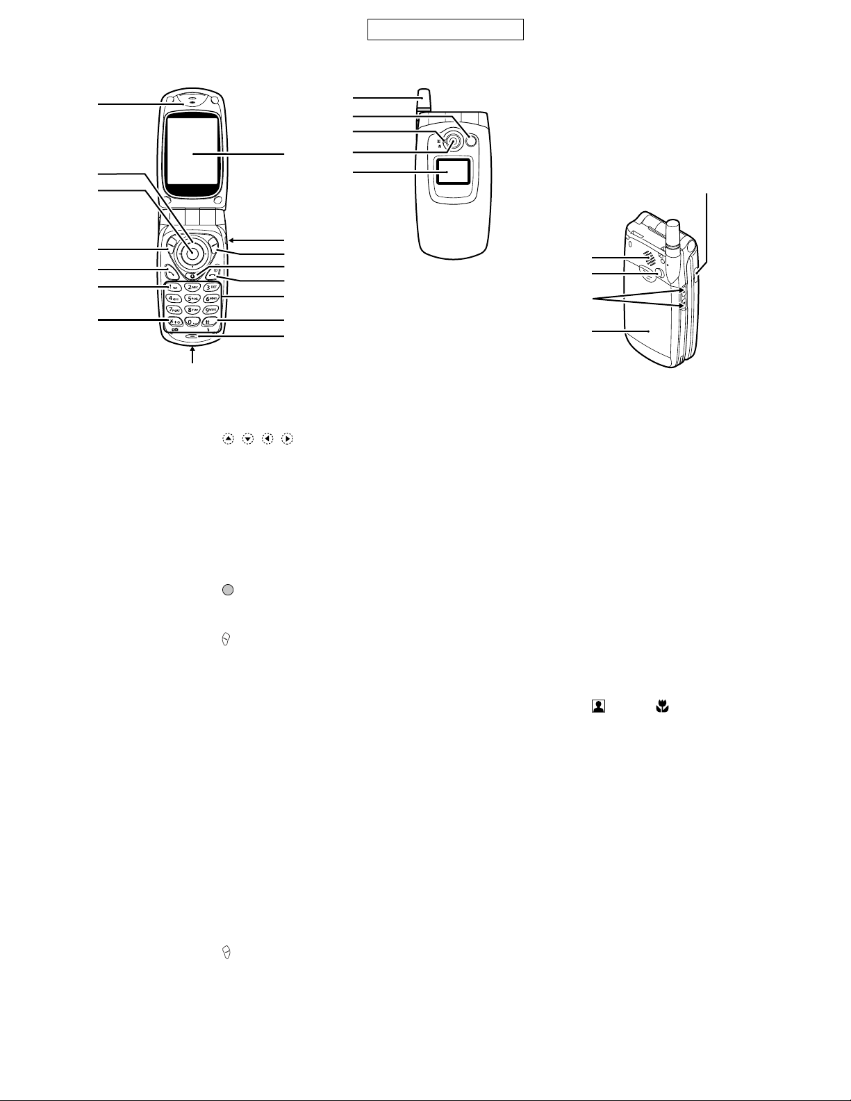
[2] Names of parts
CONFIDENTIAL
GX20
1
2
3
4
5
6
7
10
11
12
13
14
15
16
1. Earpiece
2. Navigation Keys (Arrow Keys):
Moves cursor to select
menu items, etc.
, , , in this
Up/Down arrow keys: Displays Contacts List
Left arrow key: Displays list of
Right arrow key: Displays list of Saved
3. Centre Key: Displays Main menu in
4. Left Soft Key: Executes the function at the
5. Send Key: Makes or accepts calls,
6. Voice Mail Key: Press and hold this key to
7. * /Shift Key,
Viewfinder Switch Key:
8. Main Display
9. Hands Free Connector
10. Right Soft Key: Executes the function at the
11. “Vodafone live!” Key:
manual indicate these keys.
entries in stand-by mode.
Applications in stand-by
mode.
Pictures in stand-by mode.
stand-by mode and
executes functions.
in this manual indicates
this key.
bottom left of the screen.
in this manual indicates
this key.
views the call in stand-by
mode.
connect to the Voice mail
centre automatically.
(Depends on the SIM card.)
Enters *.
Press and hold this key to
switch input method among
four modes: Abc, ABC, abc
and 123.
Switches viewfinders
between main display and
external display in digital
camera/video camera
mode.
bottom right of the screen.
in this manual indicates
this key.
Used to access “Vodafone
live!” by opening the
browser.
17
18
19
8
20
21
22
9
23
24
25
26
12. End/Power Key: Ends a call, turns power on/
13. Keypad
14. #/Flash light Key: Switches symbol screens.
15. Microphone
16. External Connector:
17. Aerial
18. Mobile Light: Usedasaflashoran
19. Macro Dial: Turns the dial to normal
(Close-up) ( ) or macro ( )
20. Camera
21. External Display
22.InfraredPort: Sends and receives data via
23. Speaker
24. RF Connector
25. Side-Up/Side-Down Keys:
26. Battery Cover
off.
Press and hold this key to
shift text input method
between multi-tap and T9
mode.
Turns the flash/auxiliary
light on or off in digital
camera/video camera
mode.
Used to connect either the
charger or data cable.
auxiliary light in digital
camera/video camera
mode, as a battery charge
indicator, or notification for
incoming calls, data/fax
calls or messages.
position.
infrared.
Moves cursor to select
menu items, adjusts
earpiece volume, etc.
In stand-by mode, press
and hold this key to turn the
mobile light on and off.
When the mobile light is
on, press this key to change
the light colour.
1 – 2
Page 4

GX20
CONFIDENTIAL
[3] Operation manual
(Page numbers refer to the user guide)
[Optional Accessories]
• Li-ion spare battery (XN-1BT11)
• High capacity Li-ion battery (XN-1BT13)
• Cigarette lighter charger (XN-1CL10)
• Data cable (RS232C cable: XN-1DC10)
• AC charger (Except for France: XN-1QC10, XN-1QC11)
(for France: XN-1QC11)
The above accessories may not be available in all regions.
For details, please contact your dealer.
[Quickstart Guide]
QUICKSTART GUIDE
1: GETTING STARTED
The Sharp GX20 is one of the most advanced mobile handsets available. With it you will be
able to use its built-in camera to take pictures and video clips, play arcade quality games,
listen to life-like polyphonic ringtones and sounds, send Multimedia messages, and connect
to Vodafone live! and the mobile internet.
But before you can do any of this, first you need to make sure your handset is prepared.
SIM card
In just a few minutes this QuickStart Guide will show you how to use
some of the main features of your new GX20.
(Except for France, Swiss)
1. Inserting your SIM card:
Slide off the battery cover, and remove the battery. Slide your Vodafone SIM card (with the
gold contacts facing downwards) into its holder. Replace the battery and cover.
2. Charging the battery:
Before using your handset for the first time, it’s important to charge the battery for at least 2
hours (see page 14 of the Manual).
3. Turning it on and off:
Open the handset, then press and hold the red key. Do the same to turn it off again.
i
softkeys.
thanks to the 5-way central navigation key and the contextual
The GX20 has many features, but exploring and using them is simple,
(In Standby): Brings up commonly used menus (Contacts List, Applications and Saved
Exit
Select
Pictures).
screen. The softkey selects the bottom right of the screen (this usually acts as
The softkey selects whatever icon or command is shown in the bottom left of the
Cancel or Back.) The key will select what’s in the middle.
(When ringing): Answers a call.
(In Standby): Brings up Last Dialled numbers.
(During call): Ends a call.
(Press and hold): Turns handset on and off.
(In menus): Takes you back to the Standby screen.
Takes you to the Vodafone live! home page.
bySHARP
ii
QUICKSTART GUIDE
2: NAVIGATION
(Centre key): Use to select an icon or menu item.
In Standby: Takes you to the main Menu (shown in phone).
In Camera mode: Takes a picture or starts/stops video recording.
(Navigation keys): Use to move between icons in menus and item lists.
Camera
G
1 – 3
Page 5
QUICKSTART GUIDE
5. Add a sound file: ( symbol in message menu bar)
G
Press [Options] and select Sound. To listen to the sounds, press [Options], then Play.
Hi there - wait til you
Highlight the sound you want, press , then press [Back].
see this!
6. Preview your message:
Then press [Options], and select Preview Message. If you’re happy with the message,
press , then again to go to the To: screen.
7. Send to another mobile:
Enter the number of the mobile phone you want to send it to. Press , then select Send
and press again. If the receiving phone can’t display Multimedia messages or video
Options Back
clips, they’ll be sent a link to a web page they can view them on.
Tip: Try sending it to yourself to see how it works!
abc
G
To:
Tip: Press [Options], then select Search in the To: screen to bring up your Contacts list.
[Back]. Then write the email address (using the key to bring up the symbols menu for
the @ key). Press , then select Send and press again.
8. Send to an email address:
After Step 6, press [Options], and select Input Method. Choose abc and then press
21/60
|
eric.wise@hotmail.com
CONFIDENTIAL
v
Then choose the mobile number or email address for the contact you wish to send it to. It
will be entered in the To: screen automatically.
Clear
Options
Vodafone live! is a mobile internet portal which is your gateway to a
new world of information, games, music and sevices.
QUICKSTART GUIDE
5: Vodafone live!
Connect to Vodafone live!:
Simply press the key (under the Navigation key) to connect you to the Vodafone live!
main menu. To exit, press the key.
Messages
New
Tip: Your GX20 uses GPRS, a fast way of getting mobile information. Also, the connection
is ‘always on’ — which means no wait for dialling up. You only pay for data you send or get,
not how long you’re connected.
Download
Chat
Games: Online fun and games to download...
Or link directly to Vodafone live! services:
In the main Menu, select the Vodafone live! section, and choose your service:
More...
Games
Ringtones: Download music, sounds and ringtones.
Search
Help &
My
Vodafone
Pictures: Download images, animations and background wallpaper.
News: Get the latest news as it happens...
This works very like an
ordinary web browser. Use
Sport: News, results and latest scores (with pictures).
Find & Seek: Get the local information you need, wherever you are.
the navigation keys to
highlight the item you want
Chat: Instant messaging and text chat with all your friends.
Search: Find what you need in Vodafone live!
to select, then press to
Tip: Vodafone live! is growing and changing all the time, so these options may vary. Keep
open that page. Press
[Back] to go back a page.
checking it out to see what’s new.
Press [Options] for the
GX20
Browser Option menu.
vi
3: THE CAMERA
QUICKSTART GUIDE
The GX20’s built-in camera now lets you take video clips, as well as
having digital zoom and even a flash. Once you’ve taken your video
iii
Save (it will be saved in My Stuff
any problems call your local Vodafone customer services.
Life is more than just text. With Multimedia Messaging you can now
enabled to send and receive Multimedia Messaging, but if you have
send videoclips, picturesand sounds as well!Your handset is already
through the Input Method (capitals, numeric, etc.).
3. Add your video clip: ( symbol in message menu bar)
Press [Options] and select Video Clip. Highlight the clip you want to send. Press ,
then press [Back].
Tip: To send video you may have to adjust the setting. Select Multimedia Messages in the
Abc
9
T
G
32KB 34/2000
Message:
Messages menu, then press [Options]. Choose Settings, Slide Show then make sure
Options
OK
see this!
(you’ll see the T9 symbol at the top of the screen). Press and hold the key to cycle
Use the keypad to write your text. To enter punctuation or other characters, press the
key, then select the symbol you want. For a space, press .
Tip: To turn Predictive Text (T9) off and on while entering text, press and hold the key
Clear
|
Options
2. Write your message:
Multimedia Messages,thenCreate Message.
1. Create a new Multimedia message:
Abc
9
T
G
Select Messages in the main Menu (or press the key in Standby mode). Select
32KB 34/2000
Message:
Hi there - wait til you
and take it again.
Tip: You can change the camera viewfinder to the external display (for taking pictures/
videos of yourself) by pressing the key. And you can adjust the Macro dial around the
in the main Menu). If not, press [Cancel], and try again.
4. Digital Camera mode:
Choose Digital Camera in the Camera menu (or press the key in Standby mode).
Macro
External
display
Press to take the picture. Press [Save] to save it (in My Stuff), or press [Cancel]
dial
keys. Then press to start recording. When you’ve finished, press again.
3. Saving your video:
Now you’ll be offered the choice of Save or Preview.ChoosePreview to review your clip,
Stop
then press [Back]. If you’re happy with the clip, select
2. Recording a video clip:
The screen becomes your viewfinder. You can zoom in (up to 4×) by pressing the key
1. Video Camera mode:
Go to the main Menu (press in Standby mode), select the Camera icon (you’ll see the
F
Fine 0 x1
16
or picture you can save it, then send it to others at a mobile number
or email address (see next page).
(the key zooms out again). You can also adjust the brightness using the and
word ‘Camera’ in the red title bar), then press . Select Video Camera.
lens to take close-up shots ( ).
QUICKSTART GUIDE
4: MULTIMEDIA MESSAGING
that Off is selected.
Picture
Sound
Video Clip
4. Add your picture: ( symbol in message menu bar)
Message Template
[Back].
Press [Options] and select Picture. Highlight the picture you want, press , then press
Text Template
Preview Message
Select Back
iv
1 – 4
Page 6

GX20
6: DOWNLOADING
QUICKSTART GUIDE
You can download from the Vodafone live! portal or the handset shortcuts (see previous
page), or use the Download More menus:
1. Download a new ringtone:
Your GX20 uses polyphonicringtones for a more life-likesound. Go to the MyStuff section
from themain Menu, choose Soundsand then Download More.Choose the ringtoneyou’d
CONFIDENTIAL
vii
menus and options screens...
more information in the manual — or you could just explore all the
Here are a few tips to help you use your new handset. There’s much
1. Silent mode:
To switch your handset to silent mode, press and hold the key. Highlight the Silent
profile and select it. Select the Normal profile to go back to your usual setting.
2. International dialling:
Press and hold the key for the (+) sign when dialling international numbers.
3. Voice Memo:
downloaded ringtone.
2. Download new background wallpaper:
To choose a new background image for your phone, go to My Stuff/Pictures/
like and follow the instructions to download it.
Tip: Toactivate your ringtone,go to Profiles (inthe main Menu),then choose Normal,then
select Options/Personalise/Assign Melody. Choose My Sounds and select your
Download More. Choose an image and follow the instructions to download it. Then go to
Settings (in the main Menu)/Phone Settings/Main Display/Wallpaper/My Pictures, and
select your downloaded image.
3. Download new games:
To addmore arcade qualitygames to yourhandset, go to Fun & Games(in the main Menu)
and choose Games & More/Download More. Choose a game to download, and you’ll find
it in Fun & Games/Games & More/Applications.
Press then to bring up theVoice Memo application.Press to record, and again
to stop. You can send voice memos as part of a Multimedia message.
4. Front light:
light onand off (itcan be usedas a makeshift torch).Press the sidekey to change the colour
(the last selection cycles through them all like a disco light).
Settings from the main Menu, then choose External Display. Now you can change the way
5. External display:
You cancustomise your External displayin the same wayas your main screen. Goto Phone
the clock looks, the background picture, even the icon displayed when there’s a call...
Press and hold the side key on the left side of the handset (in Standby mode) to turn the
Personalise your new handset by downloading new ringtones,
images and background wallpaper from Vodafone live!. All
downloads are saved in the My Stuff section of the main Menu.
Incoming Indication
Clock Display
Icon Display
LCD On/Off
Back
Select
viii
Back
1-1-3
Normal
G
Pattern 1
Ringer VolumeDownload More
Assign Melody
Vibration
Keypad Tones
Warning Tone
Power On Sound
Power Off Sound
Message Alert
Save
G
Games & More
Applications
Screensavers
Download More
Settings
TM
Javaª Information
Back
Select
QUICKSTART GUIDE
7: TIPS AND TRICKS
Voice Memo
Ready to record
G
Start Back
G
External Display
Illustration 1
Wallpaper
Backlight
LCD Contrast
1 – 5
Page 7
CONFIDENTIAL
OZ/IQ/YO/CalcGX20Service ManualTQGX20MarketE
CHAPTER 2. ADJUSTMENTS
[1] Adjustments
SHARP Program Support Tool (SPST)
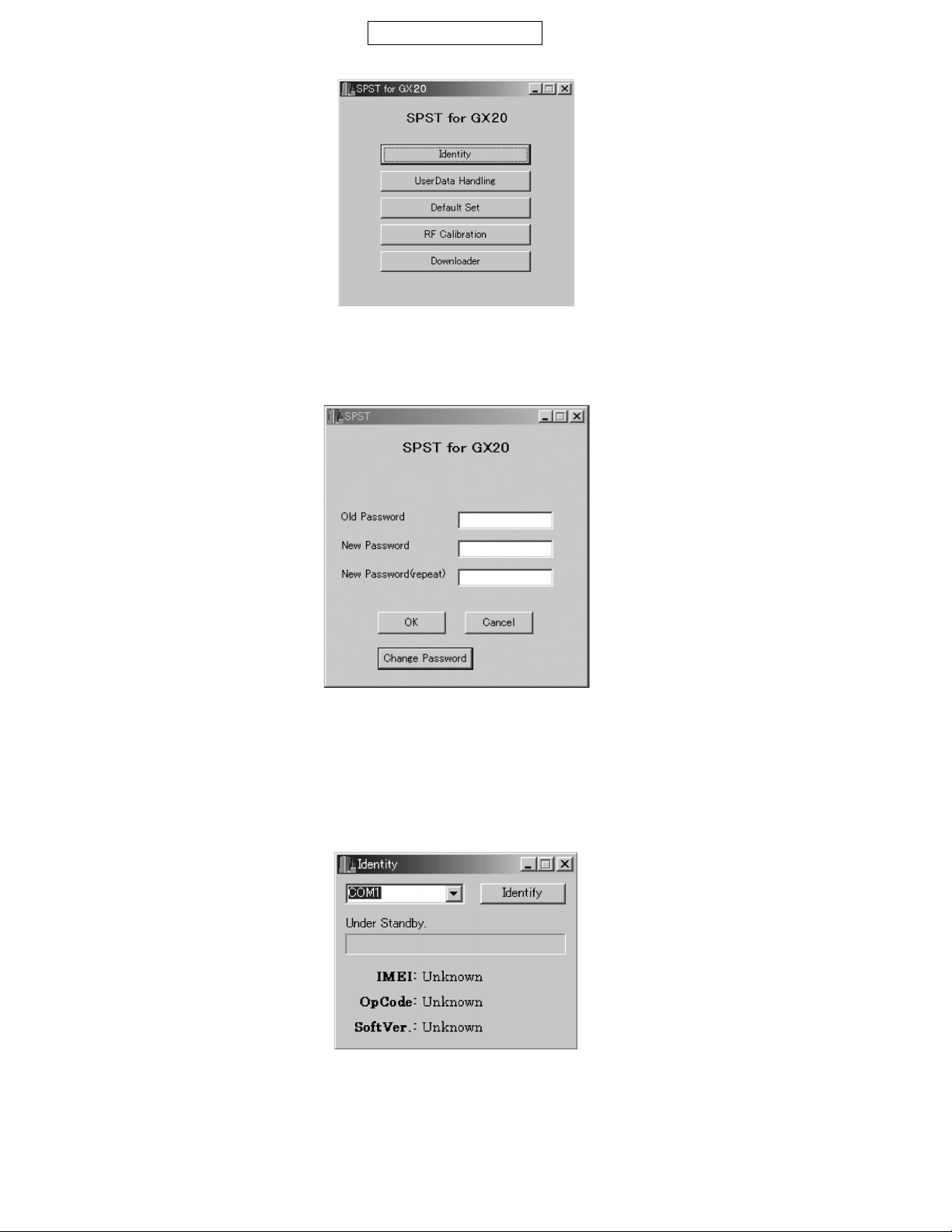
1. Outline
This document provides user information required to install and use GX20 Program Support Tool (SPST).
2. System requirements
• IBM PC compatible personal computer (standard COM1 serial port (115,200 bps) and USB required)
Supporting OS: Windows 98/98SE/2000/XP (except for Windows 95/ME/NT)
(English, German, Italian, Spanish, French and Chinese versions)
• Data cable
• Full charged battery
<During RF adjustment>
• RF test instrument: CMU200
• GPIB interface: National Instruments USB-GPIB cable
Model No.: NI GPIB-USB-B
• The battery should be fully charged.
3. Introduction
GX20
3.1. Functions
SPST offers five key functions:
1. Software download
2. User data transfer (processes all data at once but not individually)
3. RF calibration
4. Default setting
5. Identification
SPST functions as a launcher for these independent software programs.
3.2. Installation
The SPST software is distributed in CD-ROM format.
1) Use Windows Explorer and copy “UpgradingTool.zip” and “SPST.zip” to the desktop.
2) Unzip and install “UpgradingTool.zip” following the procedures below.
3) Unzip the “SPST.zip”.
Hereinafter, procedures are carried out in the SPST folder.
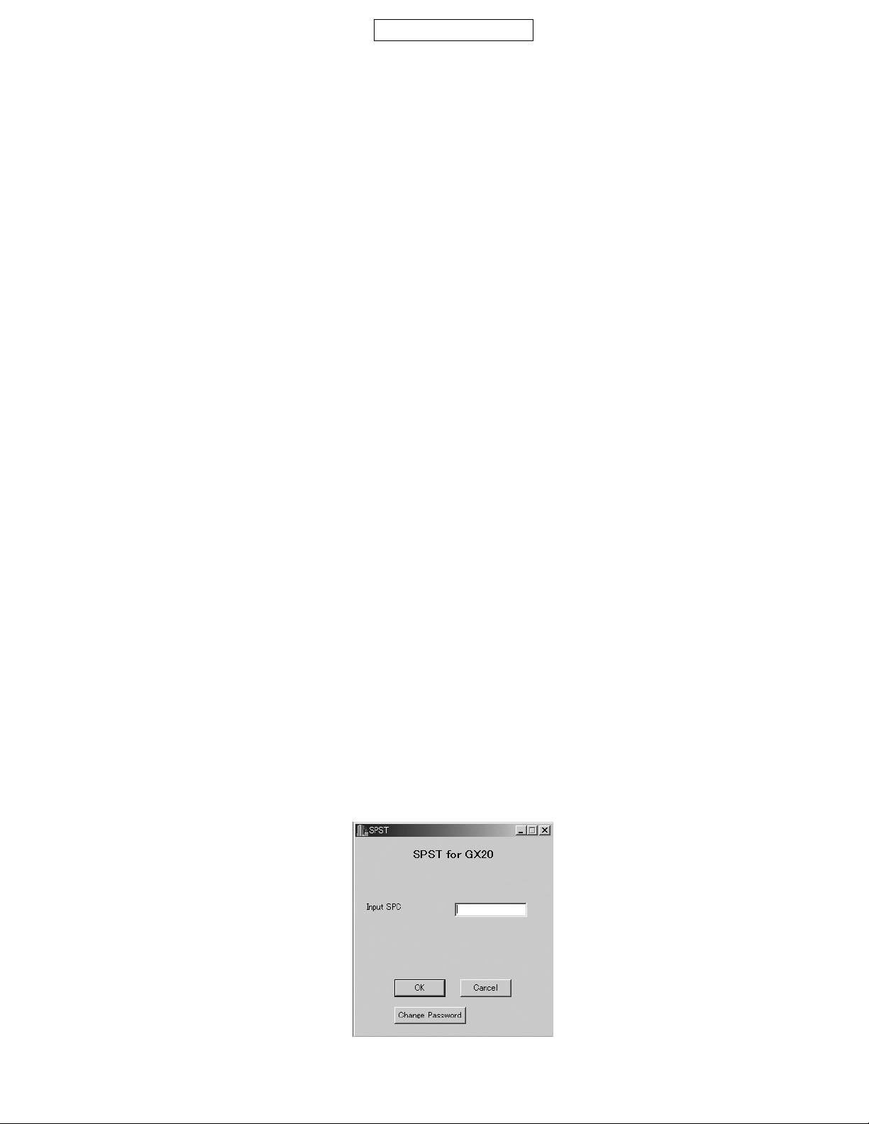
3.2.1 Starting up
Connect GX20 to an operable serial port of the PC with the supplied data cable. Connect the AC charger to the Data cable.
Execute the GX20 SPST.exe program in the SPST folder.
1) The SPC input screen appears. Input SPC (2968) and press “OK”.
If you do not know SPC, press “Cancel” to close.
Figure 1
2 – 1
Page 8
GX20
2) If SPC is correct, the following screen appears.
The software for each function is independent and thus multi-bootable. However, you can only activate single software at a time. To start snother
software, exit the current one.
3) Click the “Change Password” button in Step 1. The screen below appears and you can change SPC.
CONFIDENTIAL
Figure 2
3.3. Functions
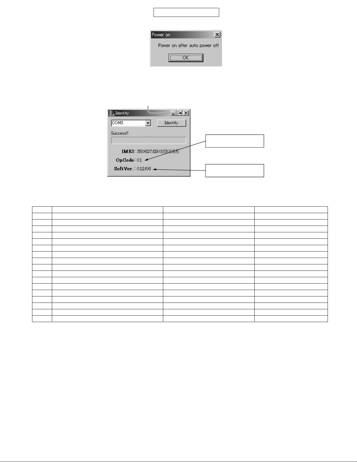
3.3.1 Identification
SPST downloads and displays the main data configured in GX20.
<Operation>
1) On the SPST startup screen, press “Identity”.
2) Connect PC and MS with a Data cable.
3) Remove the SIM card and turn on the phone. → Regular display.
4) Select the COM port.
5) Press “Get Identity”. → The information will be displayed.
Figure 3
Figure 4
2 – 2
Page 9
CONFIDENTIAL
6) IMEI will be displayed, and the following dialog box appears.
7) Make sure GX20 is turned off and press the power key.
8) Press “OK” when **** appears on the GX20 display.
9) Make sure “Success!!” appears. Check the data and exit.
GX20
Figure 5
Refer to the attachment 1
for the operator code.
Software version: 012
IMEISV: 06
Figure 6
Attachment 1 Operator Code Chart
No. Operator name Country Model name
01 Vodafone UK Post-Paid UK A4TQGX20E
02 Airtel Post-Paid Spain A4TQGX20S
03 SFR Post-Paid France A4TQGX20F
04 Vodafone Omnitel Post-Paid Italy A4TQGX20T
05 D2 Post-Paid Germany A4TQGX20G
06 Vodafone NL Post-Paid Netherlands(Holland) A4TQGX20H
08 Vodafone Ireland Post-Paid Ireland A4TQGX20R
10 Vodafone Greece Post-Paid Greece A4TQGX20D
11 Vodafone Hungary Post-Paid Hungary A4TQGX20B
12 Vodafone Australia Post-Paid Australia A4TQGX20A
13 Vodafone New Zealand Post-Paid New Zealand A4TQGX20Z
14 Vodafone Sweden Post-Paid Sweden A4TQGX20W
15 Vodafone Egypt Post-Paid Egypt A4TQGX20Q
16 Vodafone Malta Post-Paid Malta A4TQGX20L
17 Swisscom Post-Paid Switzerland A4TQGX20C
48 Vodafone PT Pre-Paid Portugal A4TQGX20PP
50 Vodafone UK Pre-Paid UK A4TQGX20EP
2 – 3
Page 10
GX20
CONFIDENTIAL
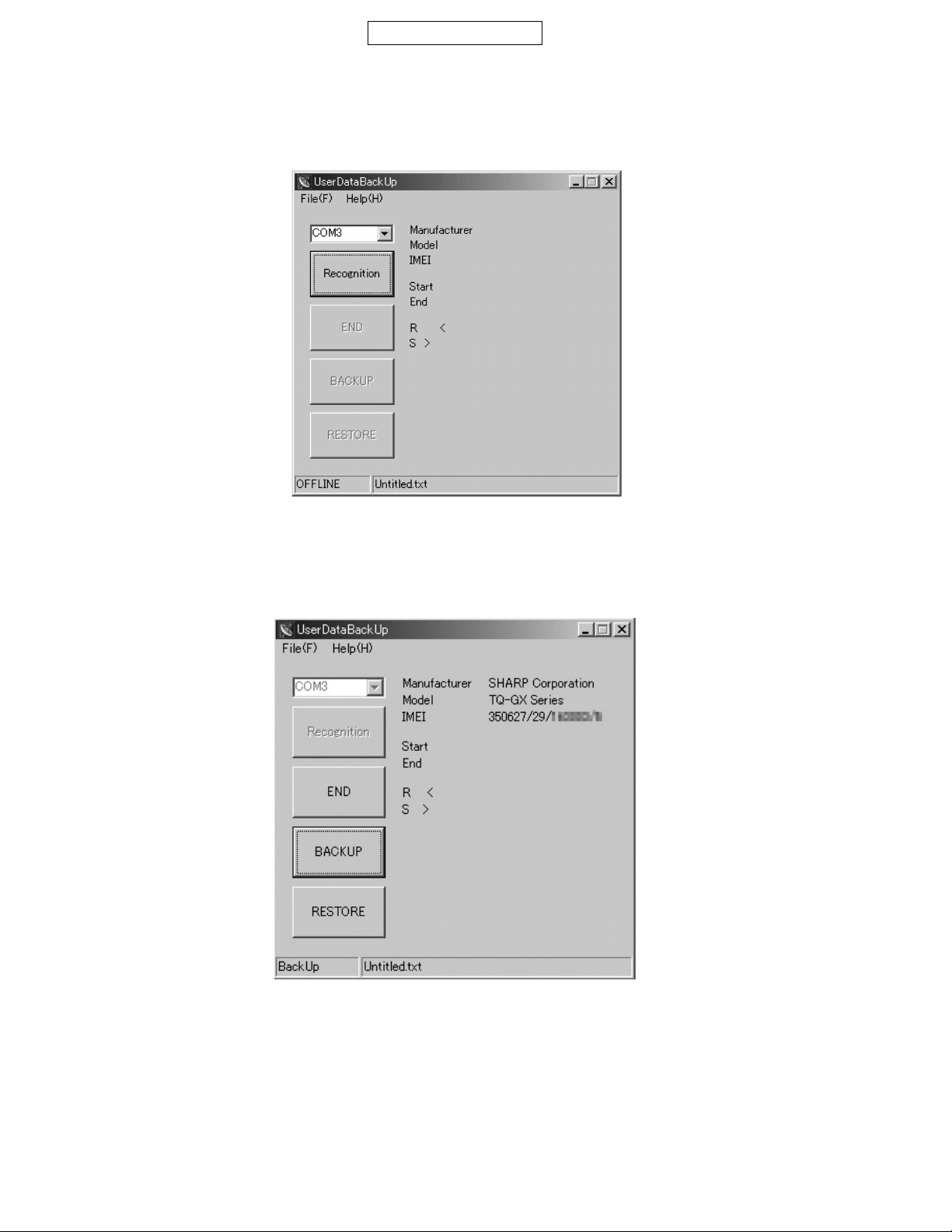
3.3.2 User data transfer
SPST saves and downloads all the following user data.
1) Connect PC and MS with a Data cable and turn on MS.
2) Activate the software.
Figure 7
a) Select the COM port. You cannot specify the communication protocol. (115 kbps)
b) Press “Recognition”.
Do not press “Recognition” until “InsertSIM” appears.
3) Press either “BACKUP”, “RESTORE” or “END”.
Figure 8
2 – 4
Page 11
CONFIDENTIAL
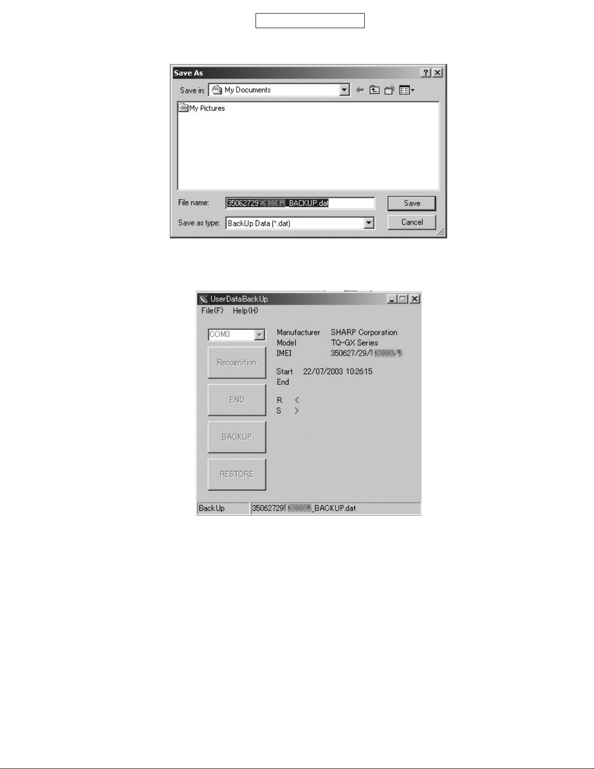
4) If “BACKUP” is pressed, the dialog box for file selection appears. Select the file and press “Save”.
Figure 9
The buttons are grayed out during the process.
GX20
Firue 10
2 – 5
Page 12
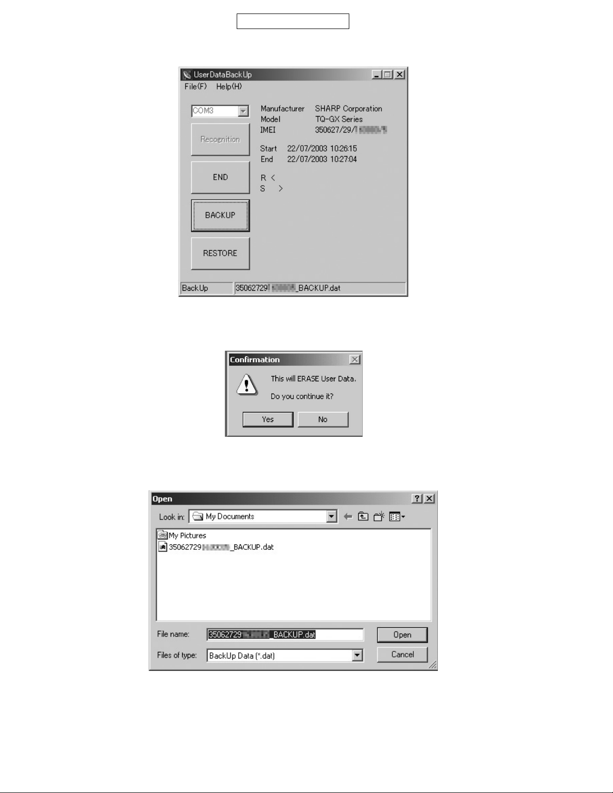
GX20
When they return to black, the process is complete. Press “END” to exit.
5) If “RESTORE” is pressed, the following confirmation dialog box appears. Press “OK” to confirm.
CONFIDENTIAL
Figure 11
Figure 12
The dialog box for file selection appears. Select the file and press “Open”.
Figue 13
2 – 6
Page 13
The buttons are grayed out during the process.
The process is complete when the buttons turn black.
CONFIDENTIAL
GX20
Figure 14
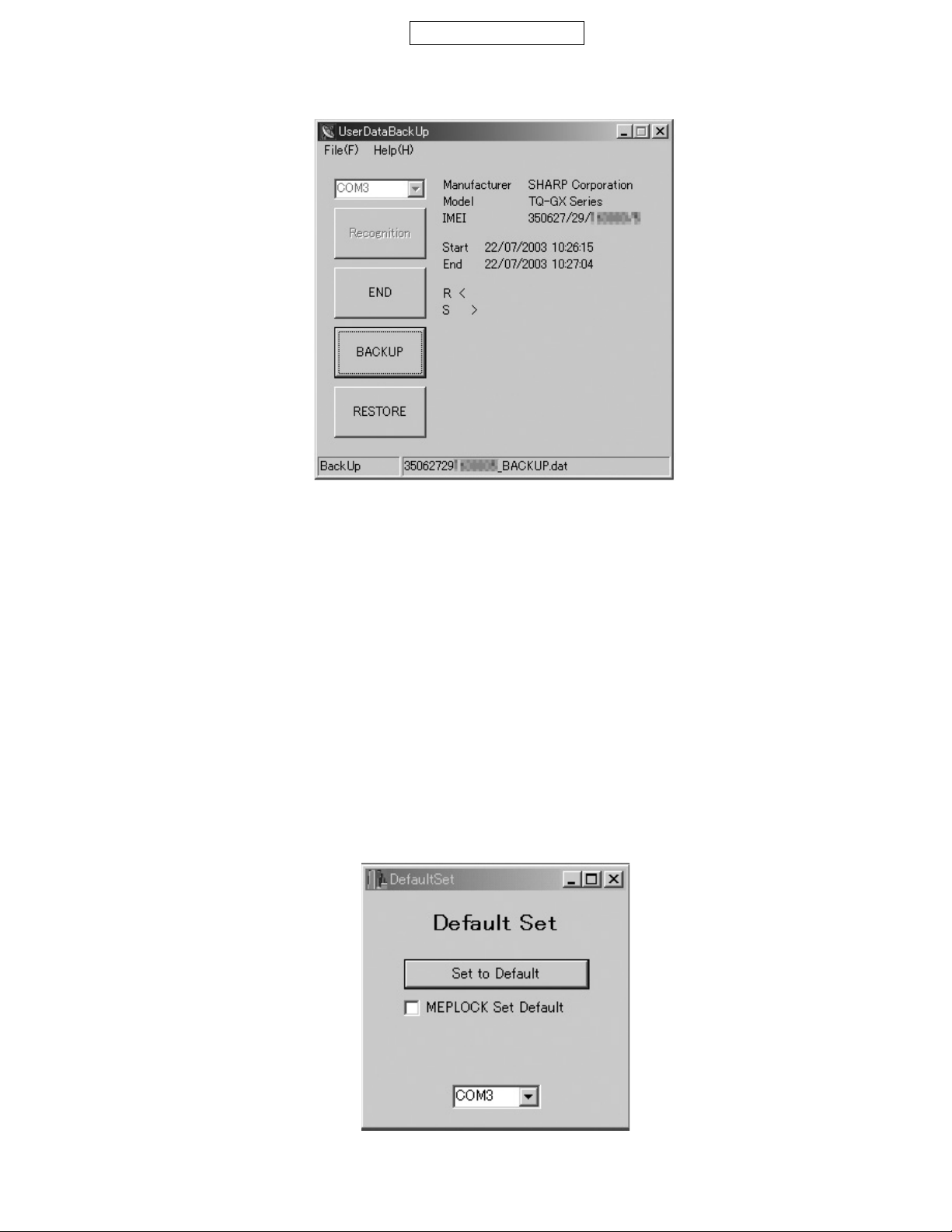
3.3.3 Default setting
You can reset settings to the factory default. The following will be performed:
1. All user data in the file system is deleted.
2. All WAP settings return to the default.
3. All values set by users return to the default.
4. 1) MEPLOCK setting remains unchanged.
When “MEPLOCK Set Default” is unchecked:
MEPLOCK remains disabled if canceled after shipment. Check “MEPLOCK Set Default” to activate it.
2) MEPLOCK setting returns to the factory default.
Check “MEPLOCK Set Default”. Even if canceled after shipment, MEPLOCK is activated.
(MEPLOCK is not activated when units are shipped to some countries and remains disabled. Check the country code.)
<Procedure>
1) Connect the cable to the phone.
2) Press the power button to enter the standby mode.
3) Click the “Set to Default” button.
Figure 15
2 – 7
Page 14
GX20
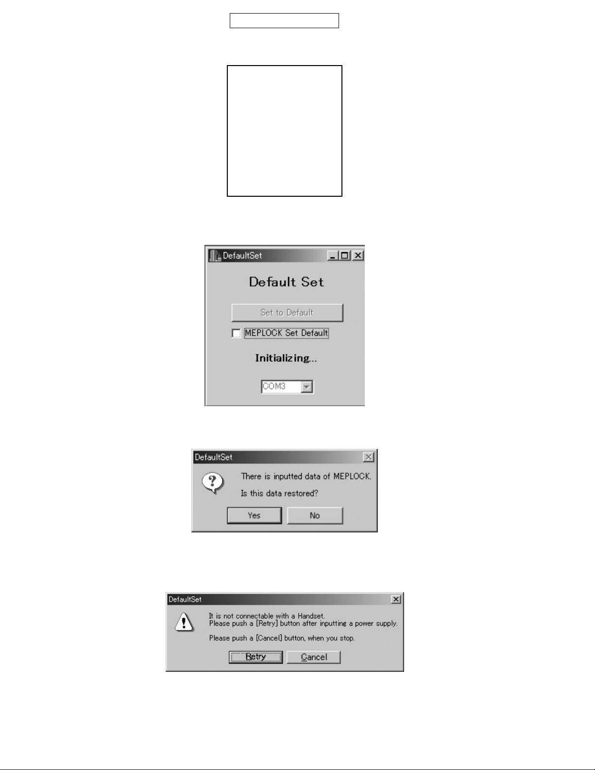
4) Click the “OK” button, The display changes as follows:
CONFIDENTIAL
H/W CHECK
ROM VERSION : 002
GX20 Diag Version. 1.3
CVS A07-005-0094-GX20
BLCD (256): 091 +001
BLCD (64k): 077
Check the version. It takes approx. 35 seconds for initialization.
∗ GX20 ∗
Figure 16
Figure 17
5) When MEPLOCK data exists, the screen below appears asking if the data should be restored. If there is no data, the screen in 8) appears.
Figure 18
6) Select [Yes]. After the following screen, turn on the phone power and click the [Retry] button.
To cancel the operation, click the [Cancel] button.
Figure 19
2 – 8
Page 15
CONFIDENTIAL
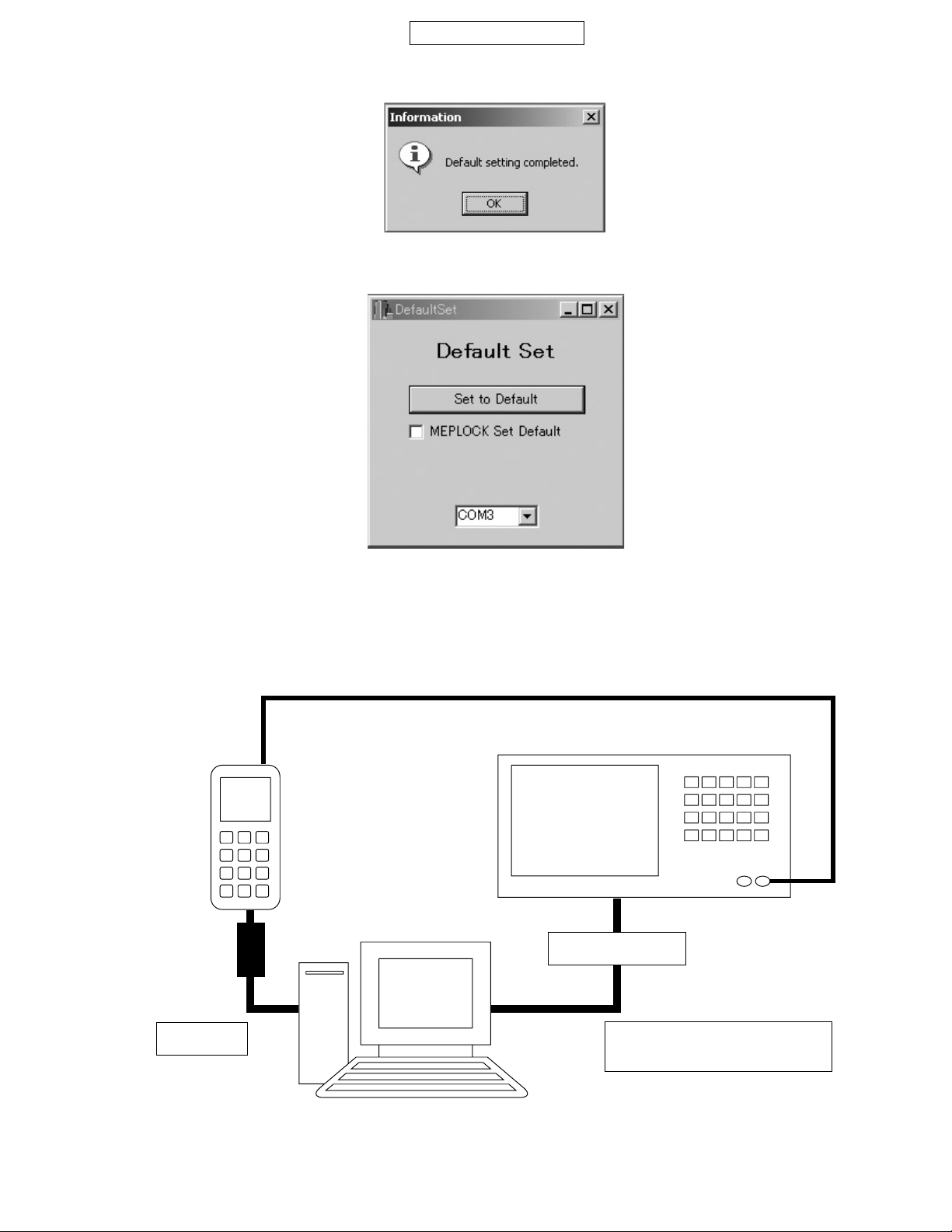
7) The screen below is displayed after initialization and the phone turns off.
Figure 20
8) Click the [OK] button. After the following screen, disconnect the cable.
GX20
The setting is completed.
3.3.4 RF Adjustment Tool
1) Tool layout
MS
Figure 21
GSM tester
GPIB cable
Data cable
Cable loss should be adjusted
according to the input value.
PC
Figure 22
2 – 9
Page 16
GX20
2) Preparation
• Connect PC and GSM tester with a GPIB cable.
• Connect PC and MS with a Data cable. (Use a full charged battery or one close.)
• Connect an antenna input/output cable of GSM tester to MS.
3) Default setting for the program.
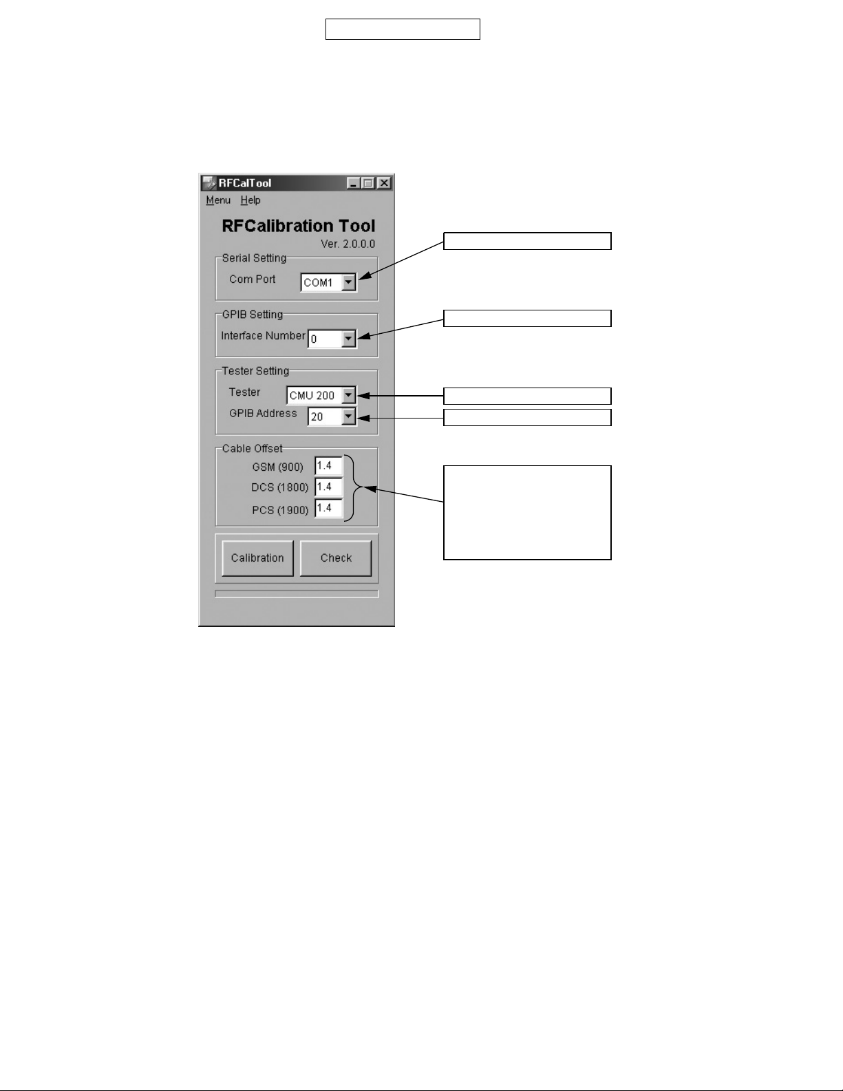
• Activate the program and set defaults.
CONFIDENTIAL
1) Select the COM port.
2) Set the GPIB No.
3) Select the test instrument.
4) Set the GPIB address.
Figure 23
5) Set the cable loss. For the
supplied cables
(YA00-0988-03), set:
GSM 0.60
DCS 0.95
PCS 0.96
2 – 10
Page 17
CONFIDENTIAL
4) RF adjustment
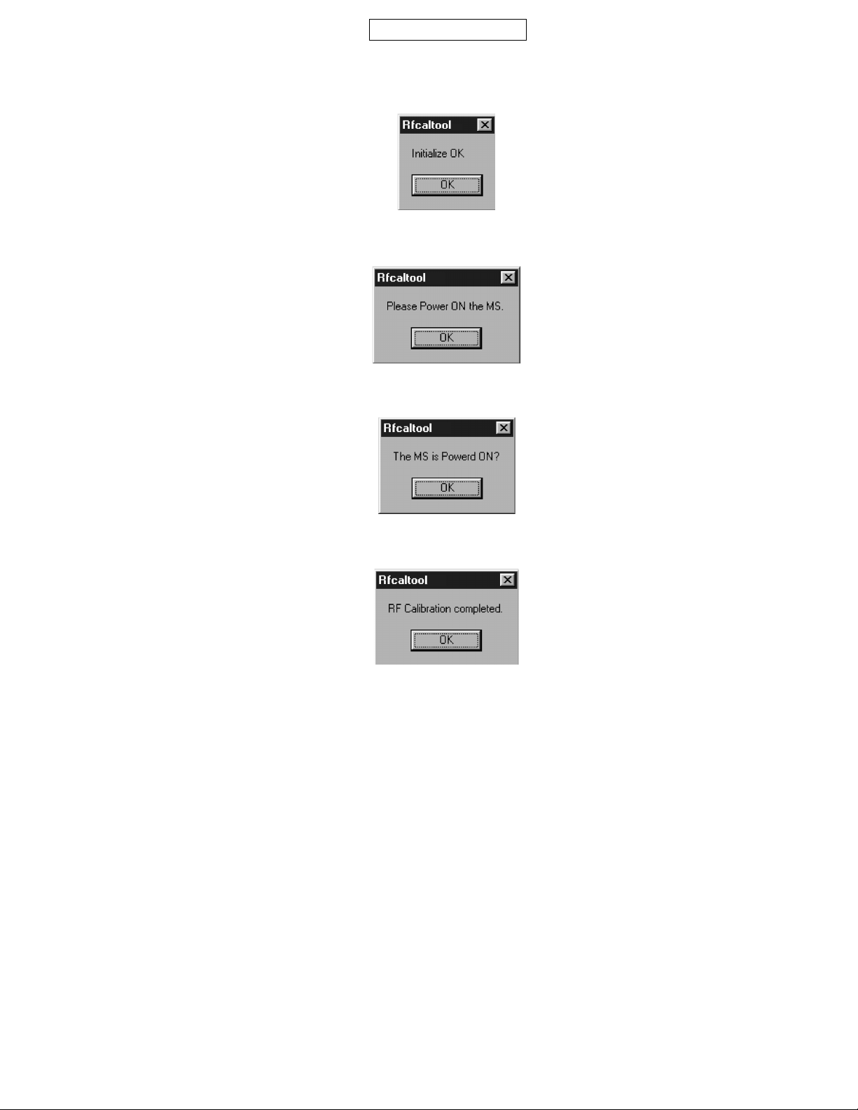
1. Press “Calibration”.
2. When initialization is complete, press “OK”.
3. Turn on the phone and press “OK”.
4. Make sure the phone is turned on and press “OK”. (Adjustments start.)
GX20
Figure 24
Figure 25
5. Press “OK”.
6. The startup screen appears.
Figure 26
Figure 27
2 – 11
Page 18
GX20
CONFIDENTIAL
5) RF performance check
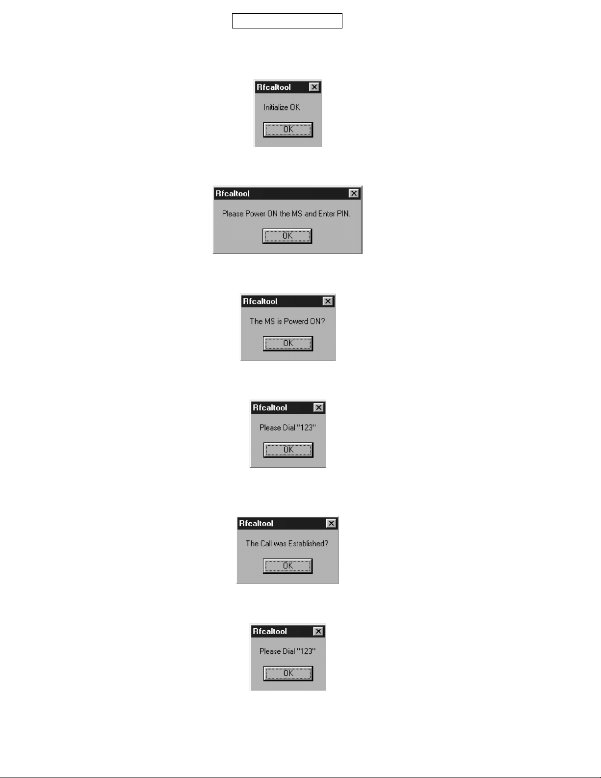
Press “Check”.
1. When initialization is complete, press “OK”.
2. Turn on the phone, enter the PIN code and press “OK”.
3. Make sure that the phone is in the idle mode and press “OK”.
Figure 28
Figure 29
Figure 30
4. Press the keys 1, 2, 3 and Send and press “OK”.
Figure 31
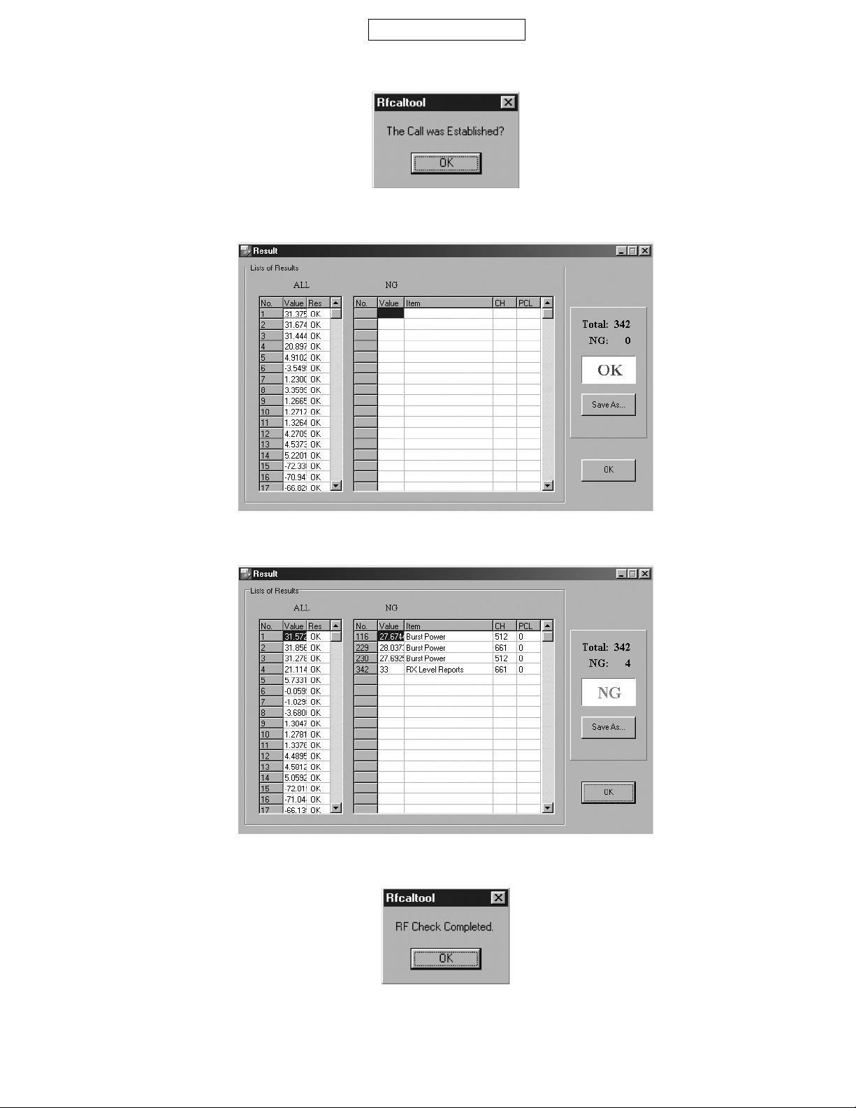
5. Make sure the terminal display is “In Call” and press “OK”.
(RF performance check starts.)
Figure 32
6. The following message appears during the check. Press the keys 1, 2, 3 and Send again and press “OK”.
Figure 33
2 – 12
Page 19
CONFIDENTIAL
7. Make sure the terminal display is “In Call” and press “OK”.
Figure 34
8. RF performance check is complete. Press “Save As…”and name the file to save the result. Press “OK” to exit.
GX20
The following will be displayed in case of failure.
9. Press “OK”.
Figure 35
Figure 36
10.The startup screen appears.
Figure 37
2 – 13
Page 20

GX20
Attachment 2
Whole inspection list by RF performance check.
Band Send-
Recei
GSM Tx 1 Sending output 37CH PCL5
band 2 Sending output 975CH PCL5
No. Item to be inspected Chan-
ing/
ve
3 Sending output 124CH PCL5
4 Sending output 37CH PCL11
5 Sending output 37CH PCL19
6 Frequency deviation 37CH PCL5
7 Frequency deviation 975CH PCL5
8 Frequency deviation 124CH PCL5
9 Phase error (RMS) 37CH PCL5
10 Phase error (RMS) 975CH PCL5
11 Phase error (RMS) 124CH PCL5
12 Phase error (Peak) 37CH PCL5
13 Phase error (Peak) 975CH PCL5
14 Phase error (Peak) 124CH PCL5
15 Mod_spectrum –800 37CH PCL5
16 Mod_spectrum –600 37CH PCL5
17 Mod_spectrum –400 37CH PCL5
18 Mod_spectrum –250 37CH PCL5
19 Mod_spectrum –200 37CH PCL5
20 Mod_spectrum +200 37CH PCL5
21 Mod_spectrum +250 37CH PCL5
22 Mod_spectrum +400 37CH PCL5
23 Mod_spectrum +600 37CH PCL5
24 Mod_spectrum +800 37CH PCL5
25 Mod_spectrum –800 975CH PCL5
26 Mod_spectrum –600 975CH PCL5
27 Mod_spectrum –400 975CH PCL5
28 Mod_spectrum –250 975CH PCL5
29 Mod_spectrum –200 975CH PCL5
30 Mod_spectrum +200 975CH PCL5
31 Mod_spectrum +250 975CH PCL5
32 Mod_spectrum +400 975CH PCL5
33 Mod_spectrum +600 975CH PCL5
34 Mod_spectrum +800 975CH PCL5
35 Mod_spectrum –800 124CH PCL5
36 Mod_spectrum –600 124CH PCL5
37 Mod_spectrum –400 124CH PCL5
38 Mod_spectrum –250 124CH PCL5
39 Mod_spectrum –200 124CH PCL5
40 Mod_spectrum +200 124CH PCL5
41 Mod_spectrum +250 124CH PCL5
42 Mod_spectrum +400 124CH PCL5
43 Mod_spectrum +600 124CH PCL5
44 Mod_spectrum +800 124CH PCL5
45 Mod_spectrum –800 37CH PCL11
46 Mod_spectrum –600 37CH PCL11
47 Mod_spectrum –400 37CH PCL11
48 Mod_spectrum –250 37CH PCL11
49 Mod_spectrum –200 37CH PCL11
50 Mod_spectrum +200 37CH PCL11
51 Mod_spectrum +250 37CH PCL11
52 Mod_spectrum +400 37CH PCL11
53 Mod_spectrum +600 37CH PCL11
54 Mod_spectrum +800 37CH PCL11
55 Mod_spectrum –800 37CH PCL19
56 Mod_spectrum –600 37CH PCL19
57 Mod_spectrum –400 37CH PCL19
58 Mod_spectrum –250 37CH PCL19
59 Mod_spectrum –200 37CH PCL19
60 Mod_spectrum +200 37CH PCL19
CONFIDENTIAL
nel
PCL
Band Send-
Recei
Rx 110 Reception sensitivity 37CH PCL5
DCS Tx 115 Sending output 699CH PCL0
band 116 Sending output 512CH PCL0
No. Item to be inspected Chan-
ing/
ve
61 Mod_spectrum +250 37CH PCL19
62 Mod_spectrum +400 37CH PCL19
63 Mod_spectrum +600 37CH PCL19
64 Mod_spectrum +800 37CH PCL19
65 Switch_Spectrum –1800 37CH PCL5
66 Switch_Spectrum –1200 37CH PCL5
67 Switch_Spectrum –600 37CH PCL5
68 Switch_Spectrum –400 37CH PCL5
69 Switch_Spectrum +400 37CH PCL5
70 Switch_Spectrum +600 37CH PCL5
71 Switch_Spectrum +1200 37CH PCL5
72 Switch_Spectrum +1800 37CH PCL5
73 Switch_Spectrum –1800 975CH PCL5
74 Switch_Spectrum –1200 975CH PCL5
75 Switch_Spectrum –600 975CH PCL5
76 Switch_Spectrum –400 975CH PCL5
77 Switch_Spectrum +400 975CH PCL5
78 Switch_Spectrum +600 975CH PCL5
79 Switch_Spectrum +1200 975CH PCL5
80 Switch_Spectrum +1800 975CH PCL5
81 Switch_Spectrum –1800 124CH PCL5
82 Switch_Spectrum –1200 124CH PCL5
83 Switch_Spectrum –600 124CH PCL5
84 Switch_Spectrum –400 124CH PCL5
85 Switch_Spectrum +400 124CH PCL5
86 Switch_Spectrum +600 124CH PCL5
87 Switch_Spectrum +1200 124CH PCL5
88 Switch_Spectrum +1800 124CH PCL5
89 Switch_Spectrum –1800 37CH PCL11
90 Switch_Spectrum –1200 37CH PCL11
91 Switch_Spectrum –600 37CH PCL11
92 Switch_Spectrum –400 37CH PCL11
93 Switch_Spectrum +400 37CH PCL11
94 Switch_Spectrum +600 37CH PCL11
95 Switch_Spectrum +1200 37CH PCL11
96 Switch_Spectrum +1800 37CH PCL11
97 Switch_Spectrum –1800 37CH PCL19
98 Switch_Spectrum –1200 37CH PCL19
99 Switch_Spectrum –600 37CH PCL19
100 Switch_Spectrum –400 37CH PCL19
101 Switch_Spectrum +400 37CH PCL19
102 Switch_Spectrum +600 37CH PCL19
103 Switch_Spectrum +1200 37CH PCL19
104 Switch_Spectrum +1800 37CH PCL19
105 Burst Timing 37CH PCL5
106 Burst Timing 975CH PCL5
107 Burst Timing 124CH PCL5
108 Burst Timing 37CH PCL11
109 Burst Timing 37CH PCL19
111 Reception sensitivity 975CH PCL5
112 Reception sensitivity 124CH PCL5
113 Floor sensitivity 2 37CH PCL5
114 Reception level report 37CH PCL5
117 Sending output 855CH PCL0
118 Sending output 699CH PCL5
119 Sending output 699CH PCL15
120 Frequency deviation 699CH PCL0
121 Frequency deviation 512CH PCL0
122 Frequency deviation 885CH PCL0
nel
PCL
2 – 14
Page 21

Band Send-
ing/
Recei
ve
CONFIDENTIAL
No. Item to be inspected Chan-
nel
123 Phase error (RMS) 699CH PCL0
124 Phase error (RMS) 512CH PCL0
125 Phase error (RMS) 885CH PCL0
126 Phase error (Peak) 699CH PCL0
127 Phase error (Peak) 512CH PCL0
128 Phase error (Peak) 855CH PCL0
129 Mod_spectrum –800 699CH PCL0
130 Mod_spectrum –600 699CH PCL0
131 Mod_spectrum –400 699CH PCL0
132 Mod_spectrum –250 699CH PCL0
133 Mod_spectrum –200 699CH PCL0
134 Mod_spectrum +200 699CH PCL0
135 Mod_spectrum +250 699CH PCL0
136 Mod_spectrum +400 699CH PCL0
137 Mod_spectrum +600 699CH PCL0
138 Mod_spectrum +800 699CH PCL0
139 Mod_spectrum –800 512CH PCL0
140 Mod_spectrum –600 512CH PCL0
141 Mod_spectrum –400 512CH PCL0
142 Mod_spectrum –250 512CH PCL0
143 Mod_spectrum –200 512CH PCL0
144 Mod_spectrum +200 512CH PCL0
145 Mod_spectrum +250 512CH PCL0
146 Mod_spectrum +400 512CH PCL0
147 Mod_spectrum +600 512CH PCL0
148 Mod_spectrum +800 512CH PCL0
149 Mod_spectrum –800 855CH PCL0
150 Mod_spectrum –600 855CH PCL0
151 Mod_spectrum –400 855CH PCL0
152 Mod_spectrum –250 855CH PCL0
153 Mod_spectrum –200 855CH PCL0
154 Mod_spectrum +200 855CH PCL0
155 Mod_spectrum +250 855CH PCL0
156 Mod_spectrum +400 855CH PCL0
157 Mod_spectrum +600 855CH PCL0
158 Mod_spectrum +800 855CH PCL0
159 Mod_spectrum –800 699CH PCL5
160 Mod_spectrum –600 699CH PCL5
161 Mod_spectrum –400 699CH PCL5
162 Mod_spectrum –250 699CH PCL5
163 Mod_spectrum –200 699CH PCL5
164 Mod_spectrum +200 699CH PCL5
165 Mod_spectrum +250 699CH PCL5
166 Mod_spectrum +400 699CH PCL5
167 Mod_spectrum +600 699CH PCL5
168 Mod_spectrum +800 699CH PCL5
169 Mod_spectrum –800 699CH PCL15
170 Mod_spectrum –600 699CH PCL15
171 Mod_spectrum –400 699CH PCL15
172 Mod_spectrum –250 699CH PCL15
173 Mod_spectrum –200 699CH PCL15
174 Mod_spectrum +200 699CH PCL15
175 Mod_spectrum +250 699CH PCL15
176 Mod_spectrum +400 699CH PCL15
177 Mod_spectrum +600 699CH PCL15
178 Mod_spectrum +800 699CH PCL15
179 Switch_Spectrum –1800 699CH PCL0
180 Switch_Spectrum –1200 699CH PCL0
181 Switch_Spectrum –600 699CH PCL0
182 Switch_Spectrum –400 699CH PCL0
183 Switch_Spectrum +400 699CH PCL0
184 Switch_Spectrum +600 699CH PCL0
PCL
GX20
Band Send-
Recei
Rx 224 Reception sensitivity 699CH PCL0
PCS Tx 229 Sending output 661CH PCL0
band 230 Sending output 512CH PCL0
(CMU
200 232 Sending output 661CH PCL5
only) 233 Sending output 661CH PCL15
No. Item to be inspected Chan-
ing/
ve
185 Switch_Spectrum +1200 699CH PCL0
186 Switch_Spectrum +1800 699CH PCL0
187 Switch_Spectrum –1800 512CH PCL0
188 Switch_Spectrum –1200 512CH PCL0
189 Switch_Spectrum –600 512CH PCL0
190 Switch_Spectrum –400 512CH PCL0
191 Switch_Spectrum +400 512CH PCL0
192 Switch_Spectrum +600 512CH PCL0
193 Switch_Spectrum +1200 512CH PCL0
194 Switch_Spectrum +1800 512CH PCL0
195 Switch_Spectrum –1800 855CH PCL0
196 Switch_Spectrum –1200 855CH PCL0
197 Switch_Spectrum –600 855CH PCL0
198 Switch_Spectrum –400 855CH PCL0
199 Switch_Spectrum +400 855CH PCL0
200 Switch_Spectrum +600 855CH PCL0
201 Switch_Spectrum +1200 855CH PCL0
202 Switch_Spectrum +1800 855CH PCL0
203 Switch_Spectrum –1800 699CH PCL5
204 Switch_Spectrum –1200 699CH PCL5
205 Switch_Spectrum –600 699CH PCL5
206 Switch_Spectrum –400 699CH PCL5
207 Switch_Spectrum +400 699CH PCL5
208 Switch_Spectrum +600 699CH PCL5
209 Switch_Spectrum +1200 699CH PCL5
210 Switch_Spectrum +1800 699CH PCL5
211 Switch_Spectrum –1800 699CH PCL15
212 Switch_Spectrum –1200 699CH PCL15
213 Switch_Spectrum –600 699CH PCL15
214 Switch_Spectrum –400 699CH PCL15
215 Switch_Spectrum +400 699CH PCL15
216 Switch_Spectrum +600 699CH PCL15
217 Switch_Spectrum +1200 699CH PCL15
218 Switch_Spectrum +1800 699CH PCL15
219 Burst Timing 699CH PCL0
220 Burst Timing 512CH PCL0
221 Burst Timing 855CH PCL0
222 Burst Timing 699CH PCL5
223 Burst Timing 699CH PCL15
225 Reception sensitivity 512CH PCL0
226 Reception sensitivity 855CH PCL0
227 Floor sensitivity 2 699CH PCL0
228 Reception level report 699CH PCL0
231 Sending output 810CH PCL0
234 Frequency deviation 661CH PCL0
235 Frequency deviation 512CH PCL0
236 Frequency deviation 810CH PCL0
237 Phase error (RMS) 661CH PCL0
238 Phase error (RMS) 512CH PCL0
239 Phase error (RMS) 810CH PCL0
240 Phase error (Peak) 661CH PCL0
241 Phase error (Peak) 512CH PCL0
242 Phase error (Peak) 810CH PCL0
243 Mod_spectrum –800 661CH PCL0
244 Mod_spectrum –600 661CH PCL0
245 Mod_spectrum –400 661CH PCL0
246 Mod_spectrum –250 661CH PCL0
nel
PCL
2 – 15
Page 22

GX20
Band Send-
ing/
Recei
No. Item to be inspected Chan-
nel
ve
247 Mod_spectrum –200 661CH PCL0
248 Mod_spectrum +200 661CH PCL0
249 Mod_spectrum +250 661CH PCL0
250 Mod_spectrum +400 661CH PCL0
251 Mod_spectrum +600 661CH PCL0
252 Mod_spectrum +800 661CH PCL0
253 Mod_spectrum –800 512CH PCL0
254 Mod_spectrum –600 512CH PCL0
255 Mod_spectrum –400 512CH PCL0
256 Mod_spectrum –250 512CH PCL0
257 Mod_spectrum –200 512CH PCL0
258 Mod_spectrum +200 512CH PCL0
259 Mod_spectrum +250 512CH PCL0
260 Mod_spectrum +400 512CH PCL0
261 Mod_spectrum +600 512CH PCL0
262 Mod_spectrum +800 512CH PCL0
263 Mod_spectrum –800 810CH PCL0
264 Mod_spectrum –600 810CH PCL0
265 Mod_spectrum –400 810CH PCL0
266 Mod_spectrum –250 810CH PCL0
267 Mod_spectrum –200 810CH PCL0
268 Mod_spectrum +200 810CH PCL0
269 Mod_spectrum +250 810CH PCL0
270 Mod_spectrum +400 810CH PCL0
271 Mod_spectrum +600 810CH PCL0
272 Mod_spectrum +800 810CH PCL0
273 Mod_spectrum –800 661CH PCL5
274 Mod_spectrum –600 661CH PCL5
275 Mod_spectrum –400 661CH PCL5
276 Mod_spectrum –250 661CH PCL5
277 Mod_spectrum –200 661CH PCL5
278 Mod_spectrum +200 661CH PCL5
279 Mod_spectrum +250 661CH PCL5
280 Mod_spectrum +400 661CH PCL5
281 Mod_spectrum +600 661CH PCL5
282 Mod_spectrum +800 661CH PCL5
283 Mod_spectrum –800 661CH PCL15
284 Mod_spectrum –600 661CH PCL15
285 Mod_spectrum –400 661CH PCL15
286 Mod_spectrum –250 661CH PCL15
287 Mod_spectrum –200 661CH PCL15
288 Mod_spectrum +200 661CH PCL15
289 Mod_spectrum +250 661CH PCL15
290 Mod_spectrum +400 661CH PCL15
291 Mod_spectrum +600 661CH PCL15
292 Mod_spectrum +800 661CH PCL15
293 Switch_Spectrum –1800 661CH PCL0
294 Switch_Spectrum –1200 661CH PCL0
295 Switch_Spectrum –600 661CH PCL0
CONFIDENTIAL
PCL
Band Send-
No. Item to be inspected Chan-
ing/
Recei
ve
296 Switch_Spectrum –400 661CH PCL0
297 Switch_Spectrum +400 661CH PCL0
298 Switch_Spectrum +600 661CH PCL0
299 Switch_Spectrum +1200 661CH PCL0
300 Switch_Spectrum +1800 661CH PCL0
301 Switch_Spectrum –1800 512CH PCL0
302 Switch_Spectrum –1200 512CH PCL0
303 Switch_Spectrum –600 512CH PCL0
304 Switch_Spectrum –400 512CH PCL0
305 Switch_Spectrum +400 512CH PCL0
306 Switch_Spectrum +600 512CH PCL0
307 Switch_Spectrum +1200 512CH PCL0
308 Switch_Spectrum +1800 512CH PCL0
309 Switch_Spectrum –1800 810CH PCL0
310 Switch_Spectrum –1200 810CH PCL0
311 Switch_Spectrum –600 810CH PCL0
312 Switch_Spectrum –400 810CH PCL0
313 Switch_Spectrum +400 810CH PCL0
314 Switch_Spectrum +600 810CH PCL0
315 Switch_Spectrum +1200 810CH PCL0
316 Switch_Spectrum +1800 810CH PCL0
317 Switch_Spectrum –1800 661CH PCL5
318 Switch_Spectrum –1200 661CH PCL5
319 Switch_Spectrum –600 661CH PCL5
320 Switch_Spectrum –400 661CH PCL5
321 Switch_Spectrum +400 661CH PCL5
322 Switch_Spectrum +600 661CH PCL5
323 Switch_Spectrum +1200 661CH PCL5
324 Switch_Spectrum +1800 661CH PCL5
325 Switch_Spectrum –1800 661CH PCL15
326 Switch_Spectrum –1200 661CH PCL15
327 Switch_Spectrum –600 661CH PCL15
328 Switch_Spectrum –400 661CH PCL15
329 Switch_Spectrum +400 661CH PCL15
330 Switch_Spectrum +600 661CH PCL15
331 Switch_Spectrum +1200 661CH PCL15
332 Switch_Spectrum +1800 661CH PCL15
333 Burst Timing 661CH PCL0
334 Burst Timing 512CH PCL0
335 Burst Timing 810CH PCL0
336 Burst Timing 661CH PCL5
337 Burst Timing 661CH PCL15
Rx 338 Reception sensitivity 661CH PCL0
339 Reception sensitivity 512CH PCL0
340 Reception sensitivity 810CH PCL0
341 Floor sensitivity 2 661CH PCL0
342 Reception level report 661CH PCL0
nel
PCL
Troubleshooting list according to the results of RF performance check.
Test item Check parts for GSM Check parts for DCS Check parts for PCS
Tx Sending output IC831, IC881, FL811, FL801 IC831, IC881, FL816, FL801 IC831, IC881, FL816, FL801
Frequency deviation TCX951 TCX951 TCX951
Phase error VCO971, IC901, VCO851 VCO971, IC901, VCO851 VCO971, IC901, VCO851
Mod_spectrum VCO971, IC901, VCO851 VCO971, IC901, VCO851 VCO971, IC901, VCO851
Switch_spectrum VCO971, IC901, VCO851 VCO971, IC901, VCO851 VCO971, IC901, VCO851
Burst Timing IC881 IC881 IC881
Rx Reception sensitivity FL801, FL901 FL801, FL902 FL801, FL903
Floor sensitivity FL801, FL901 FL801, FL902 FL801, FL903
Reception level report FL801, FL901 FL801, FL902 FL801, FL903
2 – 16
Page 23
CONFIDENTIAL
3.3.5 Software download
1) Overview
This document describes the specification of the Flash-downloading tool (Upgrading Tool) used for the user service.
2) Purpose of this document
The aim of this document is to provide a sufficient description of the GX20 Upgrading Tool for readers.
3) Scope
This document covers the description of the Flash-downloading tool specification for the user service.
4) Operating environment
Operating environment for the Upgrading Tool
OS: Windows 98, 98SE, 2000 or XP
Downloadable file: Only Motorola format is available for downloading.
Communication mode: Asynchronous mode
Data length: 8 bit
Parity bit: None
Stop bit length: 1 bit
Operating environment for the loading loader
Phone: GX20
Communication mode: Asynchronous mode
Data length: 8 bit
Parity bit: None
Stop bit length: 1 bit
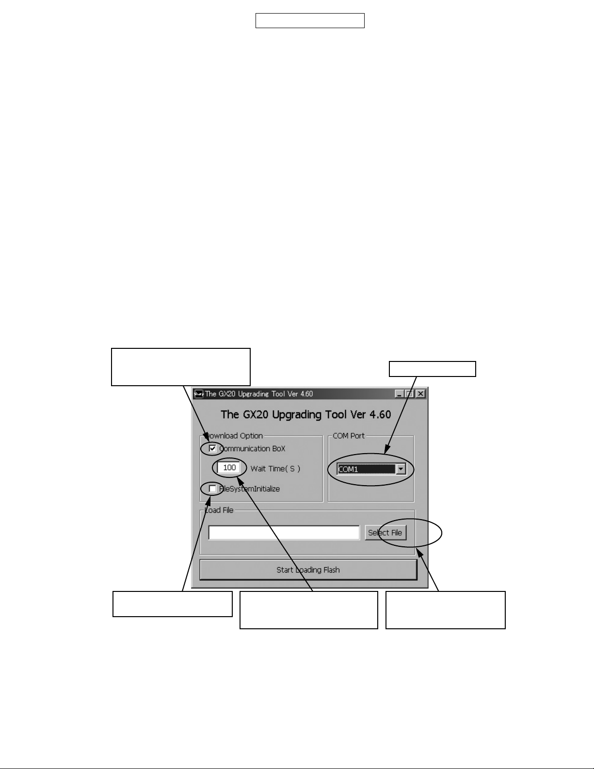
1) Description of the screens.
1) Activation
You can start the application either from the short cut on your desktop or Start menu.
2) The Upgrading Tool (on the PC)
GX20
Check here if you wish to use
"Communication Box Ver. 2G".
Note 1)
Check here if you wish
to initialize the file system.
Available when
"Communication Box Ver. 2G"
is set. Note 2)
COM port list box
Click this button to display
the dialog for selecting a
file to download.
Figure 38
2 – 17
Page 24
GX20
Note 1)
If using “Communication Box Ver. 2G”, the only the phone connected to No.1 cable is controlled on your PC.
Note2)
The time displayed in this dialog indicates a margin of processing time taken for data to be downloaded to the phones that are connected to cable
No.2 to No.10 of the “Communication Box Ver. 2G”. If an error occurs, increase this margin time. See the section 3.3.5.2 (3) “Using the Communication Box Ver. 2G” on page 2-20 for details.
[Caution!]
• If you wish to download using “Communication Box Ver. 2G”, power on from No.10 to No.1 after “Sending Sync Byte…/Press Power Button”
message has appeared.
• Use a fully charged battery and remove the check from “Communication Box” if using a Data cable for the downloading operation.
• Start downloading after the phone has been properly turned off in order to clear the Backup RAM.
• If you select “FileSystem Initialize” for the download, user’s data stored in the phone will be deleted. Care should be taken for this performance.
3) The loading loader (on the phone side)
The progress indication of the operation and error status are displayed on the phone.
The following are example screens.
CONFIDENTIAL
1. Initial screen
Flash Loader 3.10
Appears if the loading loader is
successfully expanded. (the version
of the loading loader software is
displayed). The mobile light will be
turned on to red until the write
operation is complete.
Flash Loader 3.10
COMPLETE!
2. Deleting the Flash 3. Writing the data
Flash Loader 3.10
Flash Loader 3.10
P ERASING ...
##########
Indicates a program data.
In case of the data area,
"D ERASEING" is displayed.
Indicates that the Flash is being
erased. "#" disappears as the
erasing operation proceeded.
5. SUM value is indicated Note 1)
Flash Loader 3.10
SUMCHECK END
WRITING ...
Indicates that data is being written
into the phone.
During this operation, the mobile
light stays purple.
6. Error screen Note 2)4. Writing data is completed
Flash Loader 3.10
ERS_ERROR!
SUM = XXXX h
ADR = 1000000
STR = A0
Indicates that the program data is
successfully loaded and the mobile
light will blink green light.
Note 1)
You can check if the loaded program data is correct or not by comparing the SUM values displayed on the PC side and the phone as shown on the
screen 5. If both SUM values are the same, it means the correct program data has been loaded. Please check the SUM value quickly since this display will disappear very soon if using the Data cable.
Note 2)
The screen 6 shows an example of one error occurred while in Flash erasing operation.
“ADR” and “STR” only appear for Flash-oriented errors. Other errors are described latter in section 3. (see pages 2-22, 2-23)
SUM value is displayed few
seconds after the program data has
been successfully loaded.
The value is displayed at "XXXX".
This screen appears when an error
occurs and the mobile light will blink
yellow.
ADR: Address where the error occurs.
STR: Flash Status information.
2 – 18
Page 25

CONFIDENTIAL
2) Operational specification
1) Selecting a file.
Press “Select File” button to open the dialog. Select a file you wish to download.
You can only select the file with Motorola format.
Figure 39 The dialog screen to select the file
2) Selecting a COM Port.
Select the COM Port that connects the PC and the phone (or “Communication Box Ver. 2G”) from COM Port box on the screen. You can choose
from COM1 to 9.
GX20
Figure 40 COM Port selecting screen
2 – 19
Page 26
GX20
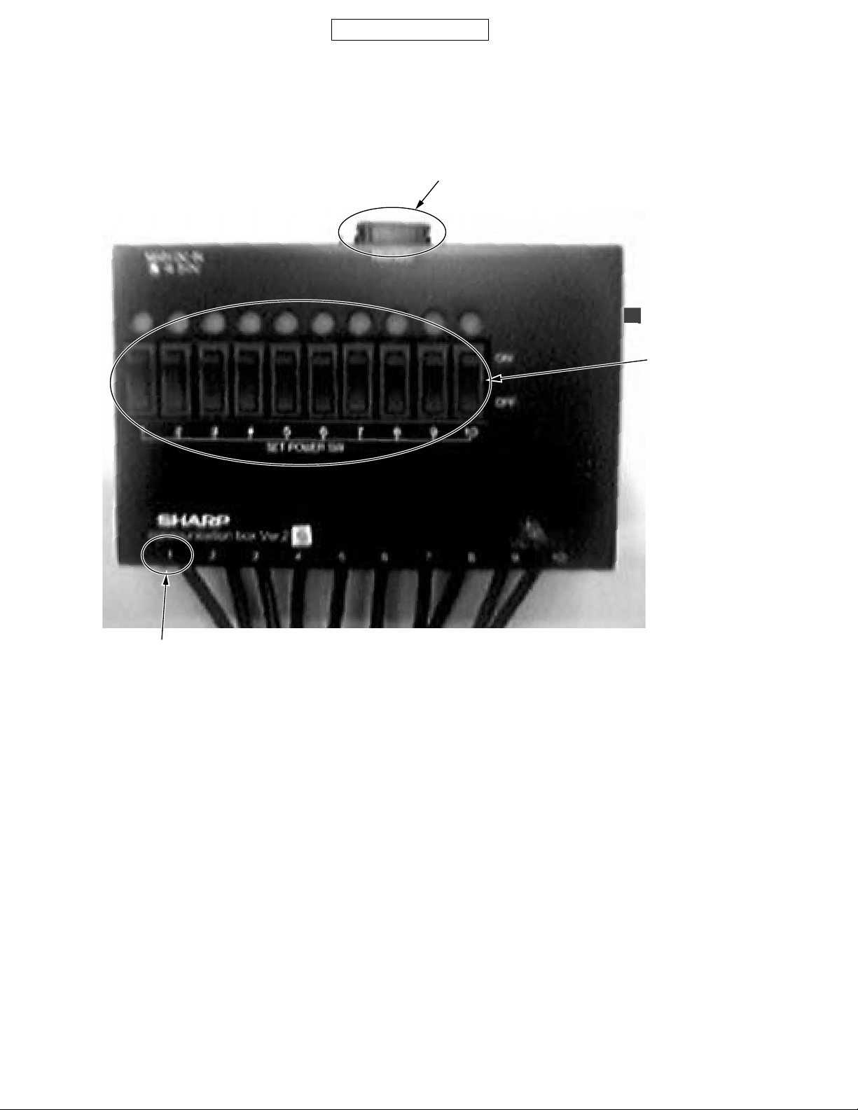
3) Using the Communication Box.
Check the dialog box “Use Communication Box Ver. 2G” displayed on your PC if using “Communication Box Ver. 2G”.
You can specify the wait time from 0 to 999 seconds since the access latency differs depending on the phone if using “Communication Box Ver.
2G”. (Default value is set to 100 seconds).
CONFIDENTIAL
Serial connection port
Power On/Off
button.
Set to OFF for
the initial status.
Cable 1.
Figure 41 Image of Communication Box Ver. 2G
[Caution]
Cable 1 is used for the handshaking between the PC and the phone. Make sure that cable is properly connected to the phone while the handshaking if using “Communication Box Ver. 2G”.
Switch on the power buttons from No.10 to No.1 when “Sending Sync Byte…/Press Power Button” message appears. You may turn on the power
switch as necessary.
2 – 20
Page 27
CONFIDENTIAL
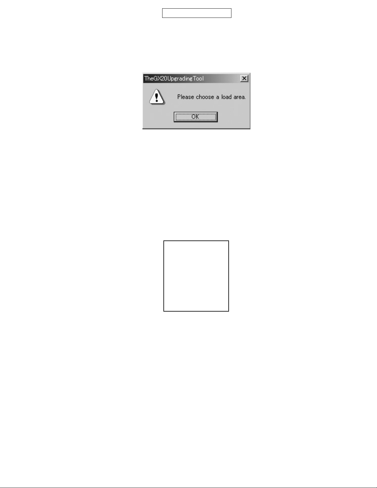
4) Starting the download.
Press [Start Loading Flash] button after you finish selecting the file to download.
Downloading operation starts. The message as below appears if no file is selected.
• Select “File System Initialize” if you wish to initialize the file system only. In this case, you can download the program by pressing the
[Start Loading Flash] button without selecting a downloading file.
Figure 42
[Using a Data cable]
If using a Data cable for the downloading operation, press Power button of the phone after [Please remove AC charger, when you use PCcableSending Sync Byte…/Press Power Button!] information message has appeared. The loading loader starts being expanded.
[Using “Communication Box Ver. 2G”]
If using “Communication Box Ver. 2G”, switch on the power button of the Box from No.10 to No.1 after [Please remove AC charger, when you use
PCcableSending Sync Byte…/Press Power Button!] information message has appeared. The loading loader starts expanding.
[Caution]
If using a Data cable, [Keep Power Button! ] message will appear after the power button of the phone is pressed. Keep pressing the button until this
message disappears. The above-mentioned message disappears and the following screen will appear after the expansion of the loading loader
has been completed.
GX20
Flash Loader 3.00
Figure 43
5) Completing the download
If the program data is successfully downloaded, [Download completed] message appears and then, the SUM value of the data loaded into the
Flash is displayed. If the operation is not properly completed, the error message will appear. Refer to pages 2-22, 2-23 [Table of Error messages]
for details of error messages.
[Caution!]
After the downloading operation is ended, SUM value is displayed on the phone.
You can check if the program data is successfully downloaded or not by comparing the SUM values displayed on the phone and the PC. Please
check the SUM value quickly since this display will disappear very soon if using the Data cable (it will disappear in about 7 seconds).
If both values are not the same, the program data may not be successfully downloaded. Please start downloading all over again.
2 – 21
Page 28

GX20
6) Matters to be attended to the downloading operation.
[If using a Data cable:]
1. Make sure to remove the AC charger from the Data cable. Otherwise it may cause the charging application to be activated and downloading operation cannot be operated properly.
2. Use a fully charged battery for the downloading operation.
3. If the battery is not charged enough, the downloading operation may not be completed. Make sure to charge the battery fully before
downloading.
4. If the downloading operation is cancelled or interrupted due to an error condition, remove the battery once and then, start over the operation.
5. Start downloading after the phone has been properly turned off in order to clear the back-up RAM.
6. If you select “FileSystem Initialize” for the download, user’s data stored in the phone will be deleted. Care should be taken for this performance.
7. If the power saving mode is set on your PC, the download may fail depending on PCs. Please cancel the power saving mode when performing the download.
[If using “Communication Box Ver. 2G”:]
1. Switch on the Power button of the Box starting from No.10 to No.1 when “Sending Sync Byte…/Press Power Button” message appears.
If the button 1 is switched on first, it results in failure of the downloading operation on phhones that are connected to the cable 2 to 10.
CONFIDENTIAL
2. The time to be taken for erasing the program data differs depending on the phones.
If failed for the erasing operation at 100 seconds wait time, increase “Wait Time”. However it takes more time to finish downloading.
3. Start downloading after turning off the phone in order to clear the back-up RAM.
4. If you select “FileSystem Initialize” for the download, user’s data stored in the phone will be deleted. Care should be taken for this performance.
5. If the power saving mode is set on your PC, the download may fail depending on PCs. Please cancel the power saving mode when performing the download.
3) Table of Error messages
1) Error messages for the Upgrading Tool (on PC side)
No. Displayed Message Description
1 Unable to open file File open error
2 Unable to receive Sync Byte Communication error
3 Cannot communicate to port Serial setting error
4 RAM Loader not responding to commands Communication error
5 RAM Loader cannot understand commands Communication error
6 Unable to program flash Flash operation error
7 Unable to reconfigure port Serial setting error
8 Select File Error Wrong file is selected.
Failed to open MOT file to download.
Could not be synchronized with Boot ROM
Wrong serial port was selected.
No response from the downloaded loading loader.
Received undefined response from the loading loader.
Failed to write or erase the Flash ROM.
Selected COM Port is still in use.
The file you select is not applicable for the upgrading.
Choose another file to download.
2 – 22
Page 29

CONFIDENTIAL
2) Table of the Loading loader error messags (on the phone side)
No. Display Message Description
1 COMPLETE! Indicates that the downloading operation is completed.
2 ERASE READY Appears while waiting for the erase operation to be ready.
3 WRITE READY Appears while waiting for the program data to be ready.
4 BRT CHANGING Appears while changing the baud rate.
5 P ERASING ... Appears while erasing the program data.
6 WRITING ... Appears while loading the program data.
7 FLASH ERS OK! Indicates that the program data is successfully erased.
8 SUMCHECK ... Appears while calculating the written data of SUM value.
9 SUMCHECK END Indicates that the calculation of the SUM value of the written data is completed.
10 SUM = XXXX h Indicates the SUM value of the written data.
11 SUM ERROR! Serial communication error (Check SUM error).
12 PARITYERR! Serial communication error (Parity bit error).
13 FRAMINGERR! Serial communication error (Framing error).
14 OVERFLOW! Serial communication error (Buffer overflow error).
15 ERS_REC_ERROR Serial communication error (Failed to receive the erase record).
16 BRT_REC_ERROR Serial communication error (Failed to receive the change record of baud rate).
17 DAT_REC_ERROR Serial communication error (Failed to receive the data record).
18 ADR_REC_ERROR Serial communication error (Failed to receive the address record).
19 END_REC_ERROR Serial communication error (Failed to receive the end record).
20 HDR_ERROR! Serial communication error (Received the undefined record).
21 ODD_ERROR! Serial communication error (Odd error).
22 SEQ_ERROR! Indicates that the Flash operation was failed (Sequence error).
23 VPP ERROR! Indicates that the Flash operation was failed (VppLow error).
24 PRT_ERROR! Indicates that the Flash operation was failed (Protect error).
25 ERS_ERROR! Indicates that the Flash operation was failed (Erase error).
26 WRT ERROR! Indicates that the Flash operation was failed (Write error).
27 ERASE CHK ERR Indicates that an error occurred while verifying the erase.
28 WRITE CHK ERR Indicates that error occurred while writing data.
29 ADR = XXXXXXXX Indicates the Flash address where the error occurred.
30 STR =XX Indicates the Flash status when the error occurred.
GX20
• From No.1 to No.10 are information messages. These messages are displayed in the normal operation.
From No.11 to 33 are error messages. Regarding to the messages from No.22 to 28, they indicate the errors that have occurred on Flash.
Address (No.29) and status information (No.30) are also displayed at the same time.
2 – 23
Page 30
GX20
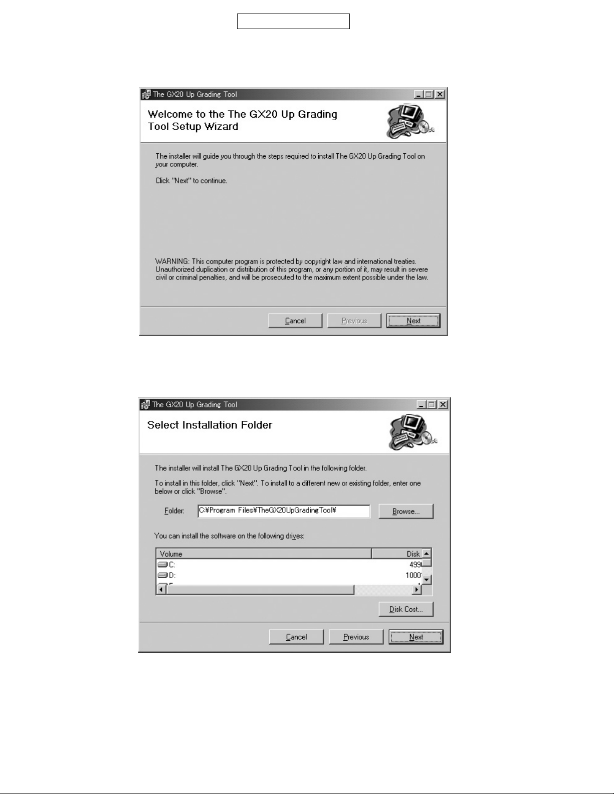
4) Installation / Un-installation
1) Installation
Execute “setup.exe” and activate the setup wizard.
CONFIDENTIAL
Select a folder you wish to install to.
Figure 44
Figure 45
2 – 24
Page 31

The confirmation screen appears. Select [Next].
CONFIDENTIAL
GX20
The Up Grading Tool is being installed.
Figure 46
Figure 47
2 – 25
Page 32

GX20
The installation is complete.
CONFIDENTIAL
Figure 48
The icon of the Up Grading Tool as shown below is configured on your desktop.
You can also activate this application selecting “The GX20 Up Ggrading Tool” from Start menu.
Figure 49 The icon of theUp Grading Tool icon
2) Un-installation
Execute “setup.exe” and activate the setup wizard.
Running “setup.exe” on the PC un-installs the preloaded program.
Check here
Figure 50
2 – 26
Page 33

The preloaded program is being un-installed.
CONFIDENTIAL
GX20
The un-installation is complete.
Figure 51
Figure 52
2 – 27
Page 34

GX20
CONFIDENTIAL
3.3.6 Matters to be attended to the Installation /Uninstallation
• If installing the Up Ggrading Tool to the PC that the tool has been already installed, uninstall the preloaded tool first then start installing the program
again.
• If you are performing the Up Ggrading Tool on Windows 98, 98SE and Me operation system, a message may appear asking you to restart up the
operation system during the installation. In this case, please restart your operation system according to the instruction. Even if such massages do
not appear, restart your operation system after the installation has been completed.
Note)
If you are using Windows 98 and trying to activate the Up Grading Tool without restarting the operation system, the following message may appear.
In this case, you need to restart your operation system for the proper operation of the Up Grading Tool.
Figure 53
Attachment 3 Reset Tool for the phone code
<Description>
Reset the phone code to “0000”.
<Operation>
1) Connect the Reset tool to the cable.
2) Execute “PWDinit.exe”.
3) Press the power key to access the idle mode. (“InsertSIM” is displayed.)
4) Press “Set to Default”.
5) Enter “2968” and press “OK”.
Figure 54
Figure 55
2 – 28
Page 35

CONFIDENTIAL
6) Press “Reset”. The following confirmation message appears.
Figure 56
7) Press “Yes” .
Figure 57
8) When initialization is complete, the dialog box below appears. Press “OK” to turn off the phone.
GX20
Figure 58
2 – 29
Page 36

GX20
[2] SHARP RF Test tool manual
1. Requirements
• PC with COM port
• Mouse
• GX20 Data Cable
• PWB repair jig
CONFIDENTIAL
Figure 59 PWB repair jig
2. Setup
1. Set PWB and make connections as shown in Figures 62 and 63.
Make sure connections are correct at the points shown in Figure 64.
2. Connect PC and GX20 with Data Cable.
3. Turn on the phone.
4. Start RF Test Tool.
5. Select a COM port to which Data Cable is connected.
6. Press the “Initialize & Read Data” Button.
7. Figure 61 appears.
8. Click OK to proceed.
Figure 60
Figure 61
2 – 30
Page 37

PWB
CONFIDENTIAL
GX20
Setting Pin
Hook
Hook
Figure 62 PWB installation
Black
Red
Setting Pin
Hook
Setting Pin
PC
Data Cable
Figure 63 Connections
2 – 31
Page 38

GX20
CONFIDENTIAL
Points
Figure 64 Contact points
Push
Figure 65 Turning power on
2 – 32
Page 39

CONFIDENTIAL
3. Tests
3.1. BAND Select & Channel
Select a band and a channel to test. Settings are applied to all tests.
Band selection
[Procedure]
1. Select a band. (GSM, DCS or PCS)
2. Select or enter a channel using Channel bar or Input box.
3.2. TX test
Test burst transmission.
TX frequency of selected channels Current PCL (Read only)
GX20
Input box
Channel bar
Figure 66
PCL bar
Data patterns
Figure 67
[Procedure]
1. Select a band and channel. (see 3.1)
2. Select PCL (Power Control Level) using PCL bar.
3. Select Data pattern.
4. Click TX ON to start burst transmission.
(You can check each part in this state.)
5. Click TX OFF to end burst transmission.
* Data pattern (TSC 5) includes Training Sequence GSM 5, and other part is pseudo random data.
TX ON/OFF button
This indicator appears during
burst transmission.
2 – 33
Page 40

GX20
GX20 TX power Table (Target power during calibration, supply voltage: 3.7[V])
GSM DCS/PCS
PCL TX Power [dBm] PCL TX Power [dBm]
5 31.6 0 28.6
6 30.0 1 27.0
7 29.0 2 26.0
8 27.0 3 24.0
9 25.0 4 22.0
10 23.0 5 20.0
11 21.0 6 18.0
12 19.0 7 16.0
13 17.0 8 14.0
14 15.0 9 12.0
15 13.0 10 10.0
16 11.0 11 8.0
17 9.0 12 6.0
18 7.0 13 4.0
19 5.0 14 2.0
CONFIDENTIAL
3.3. RX test
The phone receives burst signals in this test.
15 0.0
RX frequency of selected channels
Current RX Gain (Read only)
RX Gain Setting bar
RX ON/OFF button
This indicator appears while
Sniff ON/OFF
Figure 68
[Procedure]
1. Select a channel and band. (see 3.1)
2. Select RX Gain using RX Gain Setting bar.
3. Choose Sniff ON or OFF.
4. Click RX ON to start receiving burst signals.
5. From GSM tester, send burst signals in the specified channel.
(You can check each part in this state.)
6. Click RX OFF to end receiving burst signals.
* In this test, the reception timing cannot be synchronized with burst signals from Signal Generator or GSM tester.
* The standard RX Gain Setting is:
(Input power at the antenna connector of the phone) + (RX Gain) = –16 dBm
Excessive Input power or RX Gain may cause damage to the phone.
receiving burst signals.
2 – 34
Page 41

CONFIDENTIAL
3.4. RSSI Measure
The phone notifies you of input power value at the antenna connector.
GX20
Estimated Power
Input box
(Integer only)
Measure button
Figure 69
[Procedure]
1. Connect the phone and GSM tester (or Signal Generator) with RF cable.
2. Select a band and channel. (see 3.1)
3. Send signals (*) from GSM tester.
4. Enter the value of input power from GSM tester in integers (from –10 to –110) considering RF cable loss.
5. Press the Measure button.
6. The result appears in Measured Power box.
* The signal type from GSM tester must be either of two:
1. Continuous sine wave (without modulation) with the frequency as follows:
(Frequency of the measured channel) + 67.708kHz.
(Ex. channel: GSM 37ch → the result: 942.467708 MHz)
Power: –110 to –10 dBm
2. BCCH signal of the measured channel
Power: –110 to –10 dBm
Result
When the phone is properly calibrated, the error between “Estimated Power” and “Measured Power” is less than 2dB.
Measured power box
4. Termination
Turn off the phone to ensure proper operations.
5. Trouble imfomation
When switching DCS and PCS, change the channel number as well. Or the band does not change properly.
Example: If you change DCS 512 CH to PCS 512 CH, the band remains DCS.
2 – 35
Page 42

GX20
CONFIDENTIAL
[3] Adjustment procedures after replacement of the parts
Be sure to make adjustments to the parts as shown in the table below.
1. Adjustment to
camera temperature
IC105
IC307
Camera FPC a’ssy
Main display
External display
1. Adjustment procedures of camera temperature
1. Place a thermometer near the unit to be adjusted. Make sure the room temperature is over 0°C.
2. Attach the battery pack and then connect the Data cable.
3. Access the normal mode by holding down the “End/Power” key.
4. Send the [AT+XDIAG] command to receive the response [DIAGREADY].
5. Send the [PWRFON] command to receive the response [OK].
6. Send the [PWRDOWN] command to power off.
7. Hold down the "End/Power" key to display "****".
8. Press the "3" key to display "H/W CHECK *GX20*".
Then the test mode is started.
9. Access the TEMP ADJ mode by pressing the “ ” key, and push the “1” (1. CAM TEMP) key.
10.Temperature detected by the sensor is displayed after “Temp:”. Compare the displayed value to the room temperature.
Enter the difference as a corrected value with the “ ” key if the displayed value is higher, and use the “ ” key if it is lower.
The corrected value is displayed after “Correct:”.
11.Press the “#” key. The corrected value is registed.
12.Press the “0” key to access the initial screen of the function test mode.
13.Press the "End/Power" key to power off.
14.Connect the Data cable and then hold down the "End/Power" key to display "****".
15.Press the "2" key to display "Function Mode *GX20*".
16.Send the [PWRFOFF] command to receive the response [OK].
17.Send the [PWRDOWN] command to power off.
18.Hold down the "End/Power " key to check for the startup in the normal mode.
19.Hold down the "End/Power" key to power off.
2. Adjustment to
battery temperature
3. Main display flicker
adjustment
4. External display
contrast adjustment
5. White defect
correction
2. Adjustment procedures of battery temperature
1. Perform steps 1 – 8 of “Camera temperature adjustment procedure”.
2. Access the TEMP ADJ mode by pressing the “ ” key, and push the “2” (2.BAT TEMP) key.
3. Perform steps 10 – 19 of “Camera temperature adjustment procedure”.
2 – 36
Page 43

CONFIDENTIAL
g
)
GX20
3. Main display flicker adjustment procedure
1. Attach the battery pack.
2. Access the manual testmode.
3. Access the manual testmodeF81 (LCD Setting) by pressing the “8”, “1” and “Right Soft” keys in this order.
4. Press the “2” (2. VCOM Adjust) key.
5. Adjust the flickers on the screen to the minimum by pressing the “ ” and the “ ” keys. Make sure visually they are minimized at a distance of
about 20 cm from the inverter fluorescent lamp. (Fine adjustments to the DC voltage between display electrodes)
Enlargement
(Add a black line at every one line)
58
radationpatterns with a black line between each line of thepatterns(monochromepattern
8
6. Press the “Centre” key twice. The corrected value is registered.
7. Press the “End/Power” key to exit this mode.
Figure 70
Current set value
4. External display contrast adjustment
1. Attach the battery pack and then connect the Data cable.
2. Hold down the "End/Power" key for startup in the normal mode.
3. Send the [AT+XDIAG] command to receive the response [DIAGREADY].
4. Send the [PWRFON] command to receive the response [OK].
5. Send the [PWRDOWN] command to power off.
6. Hold down the "End/Power" key to display "****".
7. Press the "3" key to display "H/W CHECK *GX20*" and then to access the test mode.
8. Press the "8" key to show the following pattern on the external display.
Current set value
Den: 075
8 gradation pattern (Monochrome pattern)
Figure 71
9. Use “ “ or “ “ key to adjust the gradation pattern by comparing it with the other one already adjusted at the plant.
10.Press the “Centre” key to show [Save OK.] on the external display.
Then the adjusted value is entered.
11.Press the "0 key to access the initial screen of the function test mode.
12.Press the "End/Power" key to power off.
13.Connect the Data cable and then hold down the "End/Power" key to display "****".
14.Press the "2" key to display "Function Mode *GX20*".
15.Send the [PWRFOFF] command to receive the response [OK].
16.Send the [PWRDOWN] command to power off.
17.Hold down the "End/Power" key to check for startup in the normal mode.
18.Hold down the "End/Power" key to power off.
2 – 37
Page 44

GX20
CONFIDENTIAL
5. Procedures of white defect correction
1. Attach the battery pack and then connect the Data cable.
2. Access the normal mode by holding down the “End/Power” key.
3. Send the [AT+XDIAG] command to receive the response [DIAGREADY].
4. "Function Mode *GX20*"is shown on the display.
5. Cover the camera front to block off light completely.
6. Transmit the [WHC00840120000000] command.
7. Response will be received if the transmission is completed after 20 to 30 seconds. Be sure to continue to block off light during this process.
<Response to be received>
• In case of [LDDEVPRMOK]: aaaabbb will be received.
aaaa: the number of white defects
bbb: the maximum level of dark current
• In case of [LDDEVPRMNG]: 000000 will be received.
This indicates light was not blocked completely. Go back to step 6.
8. Send the [WH] command.
9. After receiving th response [OK], send the [POWDOWN] command.
10.Power off and then remove the Data cable.
* White defect correction
White defects indicate pixel defects in the image detected by the light sensor. These appear as white spots even when light is completely blocked
off (even on a black background). White defect correction solves this problem.
2 – 38
Page 45

[4] Test points
TP106
TP107
TP109
TP110
TP111
TP138
TP141
TP167
TP168
TP171
TP176
TP177
TP202
TP203
TP205
TP206
TP209
TP404
TP211
TP212
TP213
TP214
TP215
TP216
TP217
TP218
TP410
TP413
TP416
TP418
TP419
TP420
TP421
TP422
TP424
TP425
TP426
TP428
TP429
TP430
TP175
TP207
TP208
TP405
TP406
TP407
TP411
TP414
TP415
TP412
MAIN PWB-A (REAR SIDE)
CONFIDENTIAL
GX20
Figure 72 TEST POINT
TP No. Signal name TP No. Signal name TP No. Signal name
TP106 JAKMIC TP207 VCORE (1.8V) TP412 Power supply for camera (+13V)
TP107 JAKEAR TP208 VANA (2.45V) TP413 Power supply for camera (-7V)
TP109 CONT2 TP209 VMEM( 2.8V) TP414 13MHzCLK
TP110 SP1 TP211 VCCD (2.5V) TP415 CAMCLK
TP111 SP2 TP212 VEXT_CN (2.5V) TP416 Terminal for LCDC adhesion
TP138 Terminal for STACK MEMORY
adhesion check 1
TP141 Terminal for STACK MEMORY
adhesion check 2
TP213 VINT (3V)
check 1
TP214 VAMP (3V) TP418 Terminal for LCDC adhesion
TP215 VT (2.715V)
TP216 VIR (2.8V) TP419 VOUT (External display)
check 2
TP167 RECIVER_OUTP TP217 POWONKEY TP420 CS
TP168 RECIVER_OUTN TP218 VLCD (1.8V) TP421 SCLK
TP171 AUXADC6 TP404 /LCD_RESET TP422 SI
TP175 AUXADC6 TP405 VPLUS2 TP424 DCLK
TP176 VPP TP406 LEDR TP425 HSYNC
TP177 CINT TP407 LEDG TP426 VSYNC
TP202 3V TP410 Terminal for APPLICATION
TP203 VBACK (3V) TP429 Back light (LED-)
POWER adhesion check 1
TP205 VRTC (1.8V) TP411 Terminal for APPLICATION
TP206 VCAM (3.1V)
POWER adhesion check 2
2 – 39
TP428 Back light (LED+)
TP430 VDD2
Page 46

GX20
KEY PWB-B (FRONT SIDE)
CONFIDENTIAL
TP344
TP308
TP323
TP322
Figure 73 TEST POINT
TP No. Signal name
TP308 VEXT_CN
TP344 DGND
2 – 40
Page 47

KEY PWB-B (REAR SIDE)
TP321
TP348
TP307
TP306
TPB334
TP305
TP328
TP330
TP347
TP329
TPB332
CONFIDENTIAL
TPB336
TPB331
TPB333
TPB335
TP319
TP317
TP309
TP315
TP311
TP324
TP320
GX20
TP313
TP301
TP345
TP346
TP314
Figure 74 TEST POINT
TP No. Signal name TP No. Signal name
TP301 VSIM (2.85V) TP328 KEYPADCOL [1]
TP305 VVIB TP329 KEYPADCOL [2]
TP306 DGND TP330 KEYPADROW [0]
TP307 VVIB TP345 KEY_BL_ON
TP309 TXD TP346 KEY_BL_ON
TP311 ADPDET TP347 JACK_GND
TP313 RXD TP348 DGND
TP314 RTS TPB331 BATT_SENSE
TP315 CTS TPB332 DGND
TP317 VTCXO (2.9V) TPB333 BATT
TP319 VRF (2.9V) TPB334 DGND
TP320 CHGIN TPB335 BATT
TP321 CHGIN TPB336 BATT
TP324 MIC
2 – 41
Page 48

GX20
CONFIDENTIAL
[5] Troubleshooting
1. Power does not turn on.
Connect a battery with voltage of more than 4.0 V. NOTE: If the cause is damage to 4-level memory (IC106), ensure to
upload flash data before operation as initializing user area
may prevent detecting the damaged data.
Manual test mode gained?
YES
Can initialization of only user area (File System) be conducted
by Flash Loader?
YES
Does the normal mode start? 4-level stack memory (IC106) data damaged.
NO
Is the program rewritable? 4-level stack memory (IC106), and IC104 defective.
YES
After restart, the normal mode gained? Program of 4-level stack memory (IC106) transformed.
NO
4-level stack memory (IC106), and IC104 defective.
NO
NO
YES
NO
YES
(To page 2-43)
A
4-level stack memory (IC106), and IC104 defective.
2 – 42
Page 49

CONFIDENTIAL
GX20
(From page 2-42)
More than 3.6 V output at BATT terminal (TPB336)? Battery terminal defective, adhesive foreign matter at contact
Voltage of below 1.6 V applied to SENSE terminal (TPB331)? Battery or battery mounting defective.
Is fuse (FS301) connected? Blowout of fuse (FS301).
More than 3.6 V output at VBAT_S terminal (IC202 4 Pin),
VBAT_AP terminal (Between FS401 and FS402), VBAT_BB
A
NO
YES
NO
YES
NO
YES
NO
battery (CN303) terminal, or bad soldering.
• Relay FPC_A or connector CN201 defective.
• Parts connected to each VBAT line or mounting defective.
terminal (IC202 22 Pin)?
YES
Voltage of below 1.6 V applied to IC102 15 pin BATT_ SENSE
terminal (C188 signal side)?
YES
Is 4-level stack memory (IC106) properly mounted? Defective mounting of 4-level stack memory (IC106).
YES
3.0 V output at VMEM (TP209), and 1.8 V output at VCORE
(TP207), respectively?
YES
3.0 V output at VINT (TP213)? IC205 or jumper (IC205 5 pin to TP213) defective.
NO
NO
NO
NO
Relay FPC_A or connector CN201 defective.
Power supply IC (IC202) defective.
YES
32.768 kHz properly output (at X102 connected to IC104 28
pin)?
Are appearance and mounting of R132, jumper (R132 to
NO
X102 (32 kHz oscillator), R132, jumper (R132 to C149), R147
and C149 defective, or mounting defective.
Or IC104 oscillation circuit defective.
C149), R147, C149, X102 and IC104 properly given?
YES
13 MHz square waves properly output at TP414? IC102, IC103, IC403, jumper (IC102 46 pin to IC104 84 pin)
NO
13 MHz triangle waves input to IC104 142pin? IC104 defective.
NO
13 MHz triangle waves output from IC901 36 pin? Parts of IC901 36 pin to IC104 142 pin defective.
NO
2.9 V output at VTCXO (TP317)? Regulator (IC303) and C318 defective.
YES
YES
YES
YES
NO
and L405 defective or mounting defective.
TCXO (TCX951), IC901 and peripheral circuit defective.
2 – 43
Page 50

GX20
2. Incoming audio cannot be heard.
Phone
CONFIDENTIAL
Signal output at the Back light FPC earpiece contact terminal? Built-in earpiece defective or defective connection between
NO
Signal output at CN402 1 pin and 2 pin? Back light FPC or CN402 defective.
NO
Signal output at TP167/TP168? Defective connection between L103 to CN402 1 pin or L104 to
NO
Signal output at C102? L103 or L104 defective.
NO
Signal output at both ends of C120? Defective parts of L103 to IC102 62 pin and L104 to IC102 61
NO
Voltage of more than 0.5 V applied to C186 (IC102 6 pin side)
?
NO
Voltage of more than 0.5 V applied to JK301 5 pin? Parts of hands free connector JK301 5 pin to IC102 6 pin
YES
YES
YES
YES
YES
YES
YES
TP167 and TP168.
Or defective connection between Back light FPC and CN402.
CN402 2 pin.
pin.
IC102 or PWB defective.
defective or connection of Relay FPC-B with CN306 and
CN202 defective.
NO
Voltage of more than 0.5 V applied to JK301 3 pin? Hands free connector JK301 defective.
YES
NO
Voltage of more than 0.5 V applied to TP106? Parts of hands free connector JK301 3 pin to TP106 defective
YES
or connection of Relay FPC_B with CN306 and CN202 defective.
NO
Voltage of more than 2.4 V applied to Q101 3 pin? Parts of Q101 3 pin to TP106 defective.
NO
Voltage of 3 V applied to Q101 2 pin? Q101 defective.
NO
YES
YES
IC104 defective.
2 – 44
Page 51

CONFIDENTIAL
Hands free kit (Headset)
When replacing the hands free kit, output available? Hands free kit defective.
NO
Signal output at JK301 4 pin? JK301 defective or defective connection.
NO
Signal output at IC101 5 pin? Parts of hands free connector JK301 4 pin to IC101 5 pin
NO
Voltage of 3 V applied to IC101 6 pin? 3 V output at IC209 4 pin?
YES
YES
YES
NO
defective or connection of Relay FPC_B with CN306 and
CN202 defective.
Jumper (TP214 to IC209 4 pin) defective.
YES
GX20
YES
NO
3 V output at IC209 1 pin?
NO
YES
IC209 defective. IC104 defective.
Voltage of 3 V applied to IC101 1 pin? IC104 defective.
YES
Signal output at IC102 63 pin? Parts of IC102 63 pin to IC101 4 pin defective or IC101 defec-
NO
Is the voltage of 0 V applied to IC102 6 pin? IC102 defective or soldering around C186 and R184 defec-
NO
NO
YES
YES
tive.
tive.
Hands free connector JK301 or R184 defective.
2 – 45
Page 52

GX20
Hands free car kit
When replacing the hands free car kit, output available? Hands free car kit defective.
Calling available in the hands free kit mode? Refer to "Hands free kit" in Troubleshooting "Incoming
Incoming/outgoing call available with hands free car kit? Refer to Troubleshooting, "Charging impossible" (see
YES
Does Charge LED light up when connecting hands free
car kit?
NO
YES
NO
YES
CONFIDENTIAL
YES
NO
NO
audio cannot be heard" (see page 2-45).
page 2-49).
YES
More than 5 V applied to CN302 8 pin?
NO
Hands free car kit defective, or CN302 defective.
Voltage of 0 V applied to CN302 12 pin when connecting
hands free car kit?
YES
Voltage of 3 V applied to TP109 regardless of connction to
hands free car kit?
YES
Hands free car kit defective.
Voltage of 0 V applied to CN302 10 pin during a call? Defective parts of CN302 10 pin to IC104 125 pin or IC104
YES
Signal output at CN302 4 pin during a call? Hands free car kit defective.
NO
CN302, L318, R308, V311, jumper (R308 to JK301 6 pin)
or JK301 defective.
3. Audio cannot be sent/recorded.
Phone
Voltage of 0.8 to 1.8 V applied to TP324?
YES
NO
NO
NO
YES
Hands free car kit defective. Or defective parts of IC302
12 pin to IC104 20 pin and IC104 defective.
R104 or IC104 defective.
defective.
(To page 2-47)
B
NO
Voltage of 0.8 to 1.8 V applied to R112 (C129 side)? Parts of C129 to L314 defective.
NO
Voltage of more than 2.4 V applied to Q101 3 pin? Parts of Q101 3 pin to C129 defective.
NO
YES
YES
YES
Q101 defective.
Voltage of 3 V applied to Q101 2 pin?
IC104 defective.
(From page 2-47)
D
NO
2 – 46
Page 53

CONFIDENTIAL
GX20
(From page 2-46)
Voltage of approx. 1 V applied to IC102 54 pin?
Voltage of approx. 1 V applied to IC102 64 pin? IC102 defective.
Voltage of more than 2.4 V applied to Q101 3 pin?
B
NO
NO
YES
YES
YES
NO
C
(To page 2-46)
D
Parts of R110, R111, C126 and jumper (IC102 64 pin to R111)
defective or soldering defective.
Built-in microphone defective.
C
Voltage of more than 0.5 V applied to C186 (IC102 6 pin
side)?
NO
YES
defective connection between microphone and PWB.
Attach the PC board on the microphone side again or replace
the microphone. Then improvement observed?
IC102 defective.
YES
NO
Voltage of more than 0.5 V applied to JK301 5 pin? Parts of hands free connector JK301 5 pin to IC102 6 pin
YES
defective or defective connection between Relay FPC_B and
CN306, CN202.
NO
Voltage of more than 0.5 V applied to JK301 3 pin? Hands free connector JK301 defective.
NO
Voltage of more than 0.5 V applied to TP106? Parts of JK301 3 pin to TP106 defective or defective connec-
NO
Voltage of more than 2.4 V applied to Q101 3 pin?
YES
YES
YES
NO
tion between Relay FPC_B and CN306, CN202.
(To page 2-46)
D
Parts of Q101 3 pin to TP106 defective.
2 – 47
Page 54

GX20
Hands free kit (Headset)
When replacing the hands free kit, output avilable? Hands free kit defective.
NO
Voltage of 1 to 1.9 V applied to JK301 3 pin?
NO
Voltage of 1 to 1.9 V applied to TP106? Parts of L105 to JK301 3 pin defective.
NO
Voltage of more than 2.4 V applied to Q101 3 pin? Parts of Q101 3 pin to L105 defective.
NO
Voltage of 3 V applied to Q101 2 pin?
CONFIDENTIAL
YES
YES
YES
YES
YES
NO
E
Q101 defective.
IC104 defective.
G
E
Voltage of approx. 1 V applied to IC102 44 pin?
NO
Voltage of approx. 1 V applied to IC102 40 pin? IC102 defective.
NO
Voltage of more than 2.4 V applied to Q101 3 pin?
YES
Parts of R107, R108, C113 and L106 defective or soldering
defective.
YES
YES
NO
F
G
F
Voltage of 0 V applied to C186 (IC102 6 pin side)? IC102 defective or soldering around C186 and R184 defec-
NO
JK301 defective or R184 defective.
YES
tive.
2 – 48
Page 55

CONFIDENTIAL
Hands free car kit
When replacing the hands free car kit, output available? Hands free car kit defective.
NO
Calling available in the hands free kit mode? Refer to "Hands free kit" in Troubleshooting "Audio cannot be
YES
Incoming/outgoing call available with hands free car kit? Refer to "Hands Free Car Kit" in Troubleshooting "Incoming
YES
Voltage of 0 V applied to CN302 10pin during a call? Parts of CN302 10 pin to IC104 125 pin defective or IC104
YES
Signal output at CN302 11 pin during a call? Hands free car kit defective.
YES
CN302, L309, V319, C328, jumper (R309 to C328), or JK301
defective.
4. Charging impossible.
YES
NO
NO
NO
NO
sent/recorded." (see page 2-48).
audio cannot be heard" (see page 2-46).
defective.
GX20
Start the test mode, using a batterry fully charged with a specified battery charger. Check that the battery voltage is more
than 4.15 V.
Does “Red of mobile light (LED405)” turn on/off when press
“1” key by manual testmode F45 (LED setting)?
YES
Is the temperature shown in the procedure "2.BAT TEMP" of
manual testmode F42 (Temp Adjust) correct? (Measuring tolerance: ± 5 deg)
YES
Is the battery voltage of 4.15 to 4.25 V shown in the procedure
manual testmode F80 (Voltage control)?
YES
Startup in the normal mode, using a battery with the voltage of
3.3 to 3.8 V.
When inserting AC Charger in External Connector, is the voltage of approx. 5.2 V applied to IC202 7 pin?
YES
When inserting AC Charger in External Connector, is the voltage of approx. 5.2 V applied to TP321?
YES
Approx. 15 sec after inserting AC Charger in External Connector, does the voltage of TPB333 and TPB335 increase by
more than 0.05 V?
YES
Battery defective or battery cycle deteriorated.
NO
NO
NO
NO
NO
NO
Q402, R403, and mobile light (LED405) defective.
YES
Is the voltage of 3 V applied to Q402 5 pin when charge LED
(LED405) is ON?
NO
Defective connection jumper (IC104 186 pin to Q402 5 pin).
IC104 Defective.
IC307, R368, CN305, Relay FPC_A, CN201, and IC102
defective.
Defective connection between IC202 5 pin and IC102 4 pin.
IC102 and IC202 defective.
Defective connection between CN302 18 pin and IC202 7 pin.
CN302, CN306, FL303, FL304, FL307, Relay FPC_B, and
CN202 defective.
Defective connection between CN302 18 pin and IC202 7 pin.
CN302, FL303, FL304 and FL307 defective.
Defective connection between IC202 9 pin and Q305 3 pin.
R348, Q305, D303, D306, D309 and IC202 defective.
2 – 49
Page 56

GX20
5. Vibrator does not operate.
CONFIDENTIAL
Vibrator terminals contacting the land?
Dirt or foreign matter detedted at vibrator terminals and the
NO
Vibrator deformed.
(Remove foreign matter or replace parts.)
land?
Check the vibrator during operation.
YES
3 V square waves output between vibrator terminals in synchronization with vibration pattern?
NO
VBAT Voltage applied to IC302 5 pin? Soldering of IC302 defective.
YES
Signals ourput at IC302 1pin in synchronization with vibration
pattern?
NO
Signals output from IC103 19pin in synchronization with vibration pattern?
NO
Voltage of approx. 3 V applied to IC103 7 pin? Are appearance and mounting of jumper (IC103 5 pin to VINT
YES YES
YES
NO
YES
YES
NO
Vibrator defective.
IC302 defective.
CN201, Relay FPC_A and CN305 defective.
Jumper (IC103 5 pin to VINT line), C141 and C142 defective.
NO
line), C141 and C142 properly given?
IC103 or the control signal line to IC104 defective.
6. Clock is reset.
More than 2.5 V output at TP202 when a battery is fitted in the
set?
YES
More than 2.5 V output at TP203 when a battery is fitted in the
set?
YES
More than 1.5 V output at TP203 when a battery is not fitted in
the set?
YES
More than 1.2 V output at TP205 when a battery is not fitted in
the set?
YES
IC104 defective.
NO
NO
NO
NO
Regulator IC201 defective.
Voltage detecter IC204 or Q201 defective.
Defective mounting of back-up battery holder.
NO
Back-up battery holder properly mounted in Relay FPC_B?
YES
• Insufficient back-up battery capacity.
• Back-up battery defective.
• Back-up battery holder defective.
• Relay FPC_B disconnected or CN202 defective.
Regulator IC203 defective.
2 – 50
Page 57

CONFIDENTIAL
7. Speaker does not operate.
* When ring tones sound but only key touch tones do not, "Keypad Tones" are set to OFF.
* When the ring tone volume is set to “Silent”, Voice Memo is not played back.
Do speaker terminals contact with the land? Speaker defective.
YES
Resistance of 8 ohms available between the speaker terminals?
YES
Signal output at the speaker land on the Relay FPC_A? Speaker defective.
NO
Signal output at TP110/TP111? R172, R173 and CN201 defective or Relay FPC_A break-
NO
YES
VBAT_AP Voltage applied to IC103 15pin?
NO
VBAT_AP voltage applied to Relay FPC_A of R182? Relay FPC_A and CN305 defective.
YES
Does the speaker function after replacing R182? R182 defective.
NO
NO
YES
YES
NO
YES
Speaker defective.
ing defective.
GX20
NO
Voltage of approx. 3 V applied to IC103 7 pin? Jumper (IC103 5 pin to VINT line) defective.
YES
Signal output at IC103 12 pin? R122, R123 or IC103 defective.
NO
NO
YES
IC103 defective or control signal line to IC104 defective.
2 – 51
Page 58

GX20
8. Movie, Voice Memo cannot be played back.
Speaker
CONFIDENTIAL
Key pad tones and incoming-call ring tones normally ? Refer to Troubleshooting, "Speaker does not operate." (see
YES
When normally starting playback on the playback screen, is
the capacity bar changed?
YES
Ringer Volume set to "Silent"? Cancel "Silent". Then the tones normally output?
NO NO
Signal output at IC102 63 pin? Parts of IC102 63 pin to IC103 14, 13 pin defective or solder-
NO
NO
NO
YES
YES
page 2-51).
IC104 or IC106 defective.
Nondefective.
YES
ing defective.
IC102 defective.
Hands free kit (Headset)
When replacing the hands free kit, output available? Hands free kit defective.
NO
When normally starting playback on the playback screen, is
the capacity bar changed?
YES
NO
IC104 or IC106 defective.
YES
Ringer Volume set to "Silent"? Cancel "Silent". Then the tones normally output?
NO NO
YES
Nondefective.
YES
Refer to "Hands free kit" in Troubleshooting "Incoming audio
cannot be heard" (see page 2-45).
2 – 52
Page 59

9. Back light does not turn on.
CONFIDENTIAL
GX20
Do the keypad tones and ring tone sound from the speaker? Jumper (TPB333 to CN305 36, 37 pin) or Relay FPC_A,
YES
Voltage of VBAT_AP applied to FS401? Jumper (CN201 2 pin to FS401) defective or defective mount-
YES
Voltage of VBAT_AP applied to IC404 6 pin? Apparance, mounting and continuity properly given to FS401
YES
NO
NO
NO
CN305, CN201 defective.
ing.
Defective mounting or blowout of FS401.
NO
(Fuse)?
YES
C465 and C466 defective.
Only external display back light.
Which display does not light up? Main or external?
Only main display back light
or both displays' back lights.
Is the main display back light set to ON? ON Setting by the following menu.
YES
NO
NO
(To page 2-54)
H
Settings → Phone settings → Main display → Back light
Does the back light turn on?
YES
Nondefective.
When the external display
back light does not light up.
(To page 2-54)
H
Are appearance and mounting of CN402 properly given? CN402 defective.
YES
Dirt and foreign matter detected at the back light FPC terminal? Back light FPC properly inserted in CN402?
YES
NO
NO
Back light FPC defective or CN402 defective.
NO
Clean the back light FPC and insert it again. Then does it light
up?
YES
Nondefective.
Voltage of 13 to 24 V applied between TP428 to TP429? Back light FPC defective.
NO
YES
IC104 or Jumper (IC104 42 pin to IC404 4 pin) defective and
defective mounting.
NO
Does the back light slightly light up as the auxiliary light? Is the pulse shape sent to IC404 4 pin? (Don’t hold to Low?)
YES
NO
YES
IC404, L410, L411 and D413 defective.
Voltage of 3 V applied to Q404 gate (G) terminal? IC104 defective.
NO
YES
Voltage of less than 10 mV applied to Q404 drain (D) (R453
side) terminal?
YES
R453, R437 and IC404 defective.
NO
2 – 53
Q404 defective. (0.95 mV at drain terminal)
Page 60

GX20
CONFIDENTIAL
(From page 2-53)
Is the external display back light set to ON? ON Setting by the following menu.
Voltage of 3 V applied to Q403 gate (G) terminal? Defective connection between IC104 112 pin and Q403 gate
LED401, LED402 or Q403 defective.
H
YES
YES
NO
NO
NO
Settings → Phone settings → External display → Back light
Does the back light turn on?
YES
Nondefective.
(G) or IC104 defective.
2 – 54
Page 61

CONFIDENTIAL
10. "No Service" display and receiving/transmitting do not function.
10.1. "No Service" display and receiving/transmitting do not function in the EGSM band.
[Checkpoints for GSM tester transmission]
Fixed line: During input of –70 dBm.
GX20
After replacing the main PWB unit with normal one, transmission with GSM tester possible?
NO
After replacing FPC (flexible printed circuit) with normal
NO
one, transmission with GSM tester possible?
YES
YES
IC104, IC102, CN201, CN202, or PWB defective.
FPC defective.
[Checkpoints in RF Test Tool]
[Transmitting System]
Is transmission possible using RF Test Tool?
YES
Voltage applied to VCO971 7 pin? IC202, IC303, Q304, or Q308 defective.
Is VCO971 frequency fixed at 4 times as the EGSM-band
transmitting frequency + 80 MHz (or 82 MHz)?
IQ Signal input to IC901 20, 21, 22, and 23 pins? IC104, IC102, or PWB defective.
Voltage applied to VCO851 11 pin? Q304 or Q309 defective.
EGSM-Band Transmitting frequency input to IC831 1 pin? VCO851, IC901, or IC993 defective.
EGSM-Band Transmitting frequency input to FL801 11
pin?
EGSM-Band Transmitting frequency input to J801 1 pin? IC991, IC992, IC993, FL801 or FL817 defective.
NO
YES
YES
YES
YES
YES
YES
YES
NO
NO
NO
NO
NO
NO
NO
IC901, VCO971, FL971, TCX951, or IC304 defective.
FL811, R811, IC831, IC881, or IC992 defective.
J801 defective.
[Receiving System]
Fixed line: During input of –70 dBm.
Voltage applied to VCO971 7 pin? IC202, IC303, Q304, or Q308 defective.
YES
Is VCO971 frequency fixed at 4 times as the EGSM band
receiving frequency?
YES
EGSM-Band Receiving frequency signal applied to IC901
10 and 11 pins?
NO
EGSM-Band Receiving frequency signal output from
FL801 7 pin?
NO
EGSM-Band Receiving frequency signal input to FL801 9
pin?
NO
NO
NO
YES
YES
YES
IC901, VCO971, FL971, TCX951, or IC304 defective.
IC104, IC102, IC901, or PWB defective.
FL901 defective.
IC991, IC992, IC993, or FL801 defective.
J801 or FL817 defective.
2 – 55
Page 62

GX20
CONFIDENTIAL
10.2. "No Service" display and receiving/transmitting do not function in the DCS/PCS band.
[Checkpoints for GSM tester transmission]
Fixed line: During input of –70 dBm.
After replacing the main PWB unit with normal one, transmission with GSM tester possible?
NO
After replacing FPC (flexible printed circuit) with normal
NO
one, transmission with GSM tester possible?
YES
YES
IC104, IC102, CN201, CN202, or PWB defective.
FPC defective.
[Checkpoints in RF Test Tool]
[Transmitting System]
Is transmission possible using RF Test Tool?
YES
Voltage applied to VCO971 7 pin? IC202, IC303, Q304, or Q308 defective.
Is VCO971 frequency fixed at twice as the DCS (PCS)band transmitting frequency + 80 MHz (or 82 MHz)?
IQ Signal input to IC901 20, 21, 22, and 23 pins? IC104, IC102, or PWB defective.
Voltage applied to VCO851 11 pin? Q304 or Q309 defective.
DCS (PCS)-Band Transmitting frequency input to IC831 8
NO
YES
YES
YES
YES
NO
NO
NO
NO
NO
IC901, VCO971, FL971, TCX951, or IC304 defective.
VCO851, IC901, or IC993 defective.
pin?
YES
DCS (PCS)-Band Transmitting frequency input to FL801 1
pin?
YES
DCS (PCS)-Band Transmitting frequency input to J801 1
NO
NO
FL811, R811, IC831, IC881, or IC992 defective.
IC991, IC992, IC993, FL801 or FL817 defective.
pin?
YES
J801 defective.
[Receiving System]
Fixed line: During input of –70 dBm.
Voltage applied to VCO971 7 pin? IC202, IC303, Q304, or Q308 defective.
YES
Is VCO971 frequency fixed at twice as the DCS (PCS)band receiving frequency?
YES
DCS (PCS)-Band Receiving frequency signal applied to
IC901 7 and 8 (4 and 5) pins?
NO
DCS (PCS)-Band Receiving frequency signal output from
FL801 5 (3) pin?
NO
DCS (PCS)-Band Receiving frequency signal input to
FL801 9 pin?
NO
NO
NO
YES
YES
YES
IC901, VCO971, FL971, TCX951, or IC304 defective.
IC104, IC102, IC901, or PWB defective.
FL901 (FL903) defective.
IC991, IC992, IC993, or FL801 defective.
J801 or FL817 defective.
2 – 56
Page 63

11. Main display does not function.
CONFIDENTIAL
GX20
Is main display to CN404 surely inserted? Connector insertion defective.
YES
Clean the connector CN404 contact point and insert the main
display again. Does it function?
YES
Does the display function after replacement? Main display defective.
NO
More than 3.6 V output at VBAT_S terminal (IC202 4 pin),
VBAT_AP terminal (FS402 to FS401) and VBAT_BB terminal
NO
NO
YES
NO
Connector insertion part soiled.
Refer to Troubleshooting, "Power does not turn on."
(see page 2-42).
(IC202 22 pin)?
YES
Voltage of 2.8 V ± 0.1 V applied to TP209? Refer to Troubleshooting, “Power does not turn on.”
YES
More than 3.0 V ± 0.1 V applied to TP213? Refer to Troubleshooting, “Power does not turn on.”
YES
More than 1.8 V ± 0.1 V applied to TP218? Regulator IC207 or jumper (TP218 to IC207 5 pin) defective.
YES
13 MHz output at clock TP414? Refer to Troubleshooting, “Power does not turn on.”
YES
3.0 V ± 0.1 V output at LCD_RST (TP404)?
Are appearance and mounting of C417, C473 and R413 prop-
NO
NO
NO
NO
NO
(see page 2-42).
(see page 2-42).
(see page 2-42).
IC104 Defective.
Defective mounting of C417, C473 and R413.
erly given?
YES
Voltage of 3.0 V ± 0.1 V applied to CN404 34 pin, 37 pin and
38 pin?
Are appearance and mounting of jumper (CN404 34 pin to
NO
CN404, jumper (CN404 34 pin to VINT line), jumper (CN404
37 pin to VINT line), C447 and C453 defective or defective
mounting.
VINT line), jumper (CN404 37 pin to VINT line), C447 and
C453 properly given?
YES
3.0 V ± 0.1 V output at the liquid crystal reset (CN404 33 pin
and C470)?
NO
Display controller (IC403) and C470 defective or defective
mounting.
Are appearance and mounting of C470 properly given?
YES
Approx. 62 Hz of signal given to TP426?
Proper appearance and mounting given to C469, C471, C472,
NO
Display controller (IC403), C469, C471, C472 and C474
defective or defective mounting.
and C474?
YES
Normal voltage applied to the following terminal?
TP430: Approx. 10 V
Or are appearance and mounting of C450, C451, C452,
NO
Main display, CN404, C450, C451, C452, C454, C455, C457,
C458, C459, C460, C461 and Jumper (CN404 49 pin to 51
pin) defective.
C454, C455, C457, C458, C459, C460, C461 and Jumper
(CN404 49 pin to 51 pin) properly given?
YES
Main display defective.
Or defective mounting of connector CN404.
2 – 57
Page 64

GX20
12. External display does not function.
CONFIDENTIAL
Does the main display function? Refer to Troubleshooting, “Power does not turn on.”
YES
Is the external display set to ON? ON Setting by the following menu:
NO
NO
(see page 2-42).
Settings → Phone settings → External display → External display On/Off.
YES
Is external display to CN401 surely inserted? Connector insertion defective.
YES
Clean the connector CN401 contact point and insert the external display again. Does it function?
YES
Voltage of 3 V ± 0.1 V applied to CN401 27pin?
Proper appearance and mounting given to the jumper (CN401
NO
NO
NO
Connector insertion part soiled.
Jumper (CN401 27 pin to VINT Line) defective or defective
mounting.
27pin to VINT)?
YES
3.0 V ± 0.1 V output at LCD_RST (CN401 8 pin)? IC104, C417, C473 and R413 defective or defective mounting.
YES
Proper appearance and mounting given to C426, C427 and
C428?
NO
NO
C426, C427, C428 and CN401 defective or external display unit
defective.
Electric potential on the both ends of C426, C427and C428
normal?
Square waves output?
C426: Square waves of approx. 3 V
C427: Square waves of approx. 6 V
C428: Square waves of approx. 9 V
YES
Voltage of approx 11.8 V output at CN401 29pin (TP419)?
Voltage of V0 to V4 output?
NO
C418, C419, C420, C421, C423, CN401 and IC403 defective.
Control signal line to IC403, or external display unit defective.
V0 (C418): Approx. 8.56 V
V1 (C419): Approx. 7.33 V
V2 (C420): Approx. 6.11 V
V3 (C421): Approx. 2.42 V
V4 (C423): Approx. 1.20 V
YES
* The backlight turns off. After a while, the voltage at TP419 becomes approx. 9 V.
External display unit defective.
2 – 58
Page 65

13. Camera does not function.
CONFIDENTIAL
GX20
Does the camera flexible unit operate after replacement? Camera unit defective.
YES
Voltage of 2.5 V applied to TP211? Regulator IC208 or jumper (IC208 5 pin to TP211) defective.
YES
Voltage of 2.5 V applied to camera (CA1001) 2 pin? Jumper (CN101 8 pin to TP211) and CN101 defective.
YES
Voltage of 3.0 V applied to TP213? Regulator IC205 or Jumper (IC205 5 pin to TP213) defective.
YES
Voltage of 3.0 V applied to camera (CA1001) 41 pin? Jumper (CN101 12 pin to TP211) and CN101 defective.
YES
Voltage of 3.1 V applied to TP206? Voltage of 3.0 V applied to IC206 1 pin?
YES
NO
NO
NO
NO
NO
NO
Defective disconnection of Camera unit.
Defective disconnection of Camera unit.
IC104 defective.
NO
YES
Regulator IC206 defective.
Voltage of 3.1 V applied to camera (CA1001) 32 pin? Jumper (CN101 3 pin to TP206) and CN101 defective.
YES
NO
Defective disconnection of Camera unit.
IC402 or peripheral circuit defective.
IC403 or control signal line defective.
NO
Voltage of 13 V applied to TP412? Is the strobe LED normally operating?
YES
NO
YES
IC402 or peripheral circuit defective.
C184 and C411 defective.
NO
Voltage of 13 V applied to camera (CA1001) 30 pin? Are appearance and mounting of C184 and C411 properly
YES
NO
given?
YES
Jumper (CN101 10 pin to TP412) and CN101 defective.
Defective disconnection of Camera unit.
IC402 or peripheral circuit defective.
IC403 or control signal line defective.
NO
Voltage of –7 V applied to TP413? Is the strobe LED normally operating?
NO
YES
To the next page
YES
IC402 or peripheral circuit defective.
2 – 59
Page 66

GX20
From the previous page
YES
Voltage of –7 V applied to camera (CA1001) 31 pin? Are appearance and mounting of C177, C413 and R410 prop-
YES
CONFIDENTIAL
C177, C413 and R410 defective.
NO
erly given?
Jumper (CN101 5 pin to TP413) and CN101 defective.
Defective disconnection of Camera unit.
NO
YES
CAM_CLK(TP415) normally output? IC403 defective.
YES
IC104, parts of control signal lines and CN101 defective.
NO
2 – 60
Page 67

CONFIDENTIAL
14. Strobe light does not light up.
Execute the AT command (STROBOR1, STROBOG1and
STROBOB1) and then check which color does not light up
among Red, Green and Blue.
Red only
Which color does not light up?
Blue, green or three colors
Voltage of 4.35 V ± 0.75 V output at TP405? Voltage of 4.35 V ± 0.75 V output at CN201 5 pin?
YES
J
Parts of Relay FPC_A and CN201 defective or soldering
defective or CN201 5 pin connection defective.
YES
GX20
NO
Defective connection between Q201 5 pin to TP405.
Voltage of VBAT_AP applied to IC402 4, 46 pin? Q401, L402, D404 and R404 defective, or defective mounting.
NO
Apparance, mounting and continuity properly given to FS402
(Fuse)?
YES
3 V output at IC406 4 pin? IC406 and peripheral circuit defective or defective mounting.
YES
Does the camera normally function? IC402 defective.
NO
Defective control signal line between IC402 to IC403 defective.
Or IC402, IC403 defective.
YES
NO
NO
YES
Defective mounting or blowout of FS402.
NO
J
Does it light up with the AT command (STROBOR2)? Defective connection between CN201 4 pin to IC402 10 pin.
NO
Voltage of VBAT_AP applied to CN201 2 pin? Parts of Relay FPC_A and CN201 defective or soldering
NO
Parts of Relay FPC_A and CN201 defective or soldering
defective or CN201 2 pin connection defective.
YES
YES
Or IC402 defective.
defective or CN201 4 pin connection defective.
2 – 61
Page 68

GX20
15. SIM Card is not recognized.
CONFIDENTIAL
Can SIM card be recognized after replacement? SIM card defective or undesignated SIM card used.
NO
2.8 V Output at Q208 5 pin? IC104 defective.
YES
2.85 V Output at SIM power supply IC202 18 pin? IC202 or Q208 defective.
YES
Do Jumper (IC104 196 pin to CN202 24 pin) and jumper
(IC104 177 pin to CN202 25 pin)regularly output pulse
YES
NO
NO
NO
IC104 defective.
waves?
YES
Does TP301 (SIM power source) output 2.85 V?
Are appearance and mounting of jumper (CN306 17 pin to
NO
Relay FPC_A or CN306 and CN202 defective.
Or jumper (CN306 17 pin to CN301 1 pin) and C303 defective.
CN301 1 pin) and C303 properly given?
YES
Do CN301 3 pin and 6 pin regularly output pulse waves?
Are appearance and mounting of jumper (CN306 14 pin to
NO
Relay FPC_A or CN306 and CN202 defective.
Or jumper (CN306 14 pin to CN301 6 pin) and R305 defective.
CN301 6 pin) and R305 properly given?
YES
Does SIM reset signal CN301 2 pin output 3.0 V?
Are appearance and mounting of R363 properly given?
YES
Are appearance and mounting of SIM card connector (CN301)
properly given?
YES
NO
NO
Relay FPC_A or CN306 and CN202 defective.
Or R363 and IC104 defective.
SIM card connector (CN301) defective or defective mounting.
IC104 defective.
2 – 62
Page 69

16. IrDA Communications unavailable
CONFIDENTIAL
GX20
Set the specified distance and angle necessary for IrDA com-
Check in the IRDA test mode.
munications.
2.8 V output at Q207 2 pin? IC104 defective.
YES
Does IrDA power source TP216 output 2.8 V? Q207 defective.
YES
2.8 V output at UN101 6 pin? Soldering of UN101 6 pin defective.
YES
Do transmitting signals (UN101 5 pin) regularly output pulse
waves?
YES
NO
NO
NO
NO
R150 defective.
NO
Are appearance and mounting of R150 properly given?
YES
IC104 defective.
Jumper (VINT line to UN101 1 pin) and C170 defective.
NO
3.0 V output at VCC (UN101 1 pin)? Are appearance and mounting of jumper (VINT line to UN101
YES
NO
1 pin) and C170 properly given?
YES
IC104 defective.
Less than 0.2 V applied at SD signal (UN101 3 pin)? IC104 defective.
YES
Do receiving signals (UN101 4 pin) regularly output pulse
waves?
YES
Are appearance and mounting of UN101 properly given? Infrared port (UN101) defective or defective mounting.
YES
After replacement of Infrared port (UN101), communications
available?
YES
NO
NO
NO
NO
Infrared port (UN101) defective.
IC104 defective.
Infrared port (UN101) defective.
2 – 63
Page 70

GX20
CONFIDENTIAL
[6] Specification for function test
• Outline
AT commands are used for the function test mode.
To enter the general mode, send the command “AT+XDIAG”.
Then the machine can accept all key test functions (see “All Key Test and Others” on page 2-76) and further commands from the computer.
KEY Layout
Left Soft
Side
Centre
Up
Side
Down
Send End/Power
"Vodafone live!"
123
ABC DEF
456
GHI JKL MNO
789
PQRS TUV WXYZ
0
• Logic of signals
1)Setting function (AT Command: AT+XDIAG)
Asynchronous (Consisting of 115200bps, data length 8, start 1, stop 1, and Parity None).
2)After shifting to Function Test
Incoming/Outgoing serial signals should be as follows.
Right Soft
#
ST D0 D1 D2 D3 D4 D5 D6 D7 PB SP
ST: Start bit
D0-D7:Data bit
PB: Parity bit
SP: Stop bit
After AT+XDIAG
1. Synchro systemAsynchronous (Consisting of data length 8, start 1, stop 1, and Parity None)
• Signal protocol
1. The personal computer requests a response from a mobile machine to establish communications.
2. When keys are pressed, appropriate key codes are transmitted serially.
3. ASCII Characters (only capitals in the case of alphabet) are used for incoming/outgoing serial signals. At the end, return codes (0Dh, 0Ah)
are added.
4. Once making a request, the personal computer cannot make another request until the mobile machine returns a certain response. Timeout does not occur.
H
L
2 – 64
Page 71

CONFIDENTIAL
• Basic procedure (when using Hyper terminal)
Flow chart
Connect the phone to PC.
Turn on the phone.
Open Hyper terminal.
Send “AT+XDIAG” with 115200 bps and proper “ASCII setting”.
The phone is in the All key test mode. *
Send further commands to check the phone.
* : Keys are disabled if you enter the All Key test mode by AT command. To avoid this, perform steps on page 2-76.
GX20
2 – 65
Page 72

GX20
(Details)
1. Connect the phone to the computer via a data cable.
2. Turn on the phone.
3. Open Hyper terminal. (Start → Program → Accessory → Communication → Hyper terminal)
4. Enter the name and choose the desired icon. Then click “OK”.
CONFIDENTIAL
5. Choose the appropriate COM port for network and click “OK”.
Figure 75
Figure 76
2 – 66
Page 73

CONFIDENTIAL
6. Adjust the port settings and click “OK”.
7. From the file menu, select “Properties” and click the Settings tab.
GX20
Figure 77
Figure 78
2 – 67
Page 74

GX20
8. Click “ASCII setting” and check “Send line ends with line feeds” and “Echo typed characters locally”.
9. Click “OK” for “ASCII setting” and “Properties” to exit.
CONFIDENTIAL
Figure 79
Figure 80
2 – 68
Page 75

CONFIDENTIAL
10. Send “AT+XDIAG”
• You will see AATT++XXDDIIAAGG instead of AT+XDIAG as shown below by the Local echo mode, although you input AT+XDIAG.
• After sending you will receive “OK”, and the machine should enter the All key test mode (see “All Key Test and Others” on page 2-76).
GX20
Figure 81
11. You can now send commands. (See example below for the “BATVAL” command.)
Figure 82
2 – 69
Page 76

GX20
CONFIDENTIAL
1. Basic Operation Test
<Startup and initial condition>
Fit a battery or a dummy battery in the set. Hold down the “End/Power” key to start up in the general mode.
Then enter AT+XDIAG without pressing any key. → Start up in the general function test mode. (3 sec. until startup)
• Back light lights up in the standby mode.
• After startup, “Function Mode * GX20 *” is displayed.
Serial Signal Format for Basic Operation Test
Item
Main display
Back light
Red LED STROBOR 0
Green LED STROBOG 0
Blue LED STROBOB 0
External display back
light
Key back light
LED
Measuring
RTC clock
Battery voltage check
RTC Test
(Writing)
RTC Test
(Reading)
Temperature
A/D Adjustment
Temperature
check
Incoming Serial Signal Outgoing Serial Signal
Command n Response
LED 0
BKLED 0
KLED 0
OUT32K 1
BATVAL None Okn.nn Reading down to the last two digits
RTCWR yymm
RTCRD None RTC yymmddhhmmss Reading time of day
TMPAD 4
TMP n TMPnxx: Temperature
1
2
1
2
1
2
1
1
1
0
ddhh
mmss
3
2
1
Contents Test Method
OFF
Main display back light
(Brightness 4) ON
Main display standby ON
STROBORn Red OFF
STROBOGn Green OFF
STROBOBn Blue OFF
BKLEDn External display back light OFF.
KLEDn OFF
OUT32Kn 32 kHz Output (MON Output)
OK Writing time of day
ADSETOK
TMPADH <Readout AD
value>
TMPADL <Readout AD
value>
TMPADRDY
NG: Except 0 – 50 ºC
OFF
Main display back light
(Brightness 4) ON.
Main display standby ON.
Red strobe light ON
(IC402 control).
Red strobe light ON
(IC104 control).
Green strobe light ON
(IC402 control).
Green strobe light ON
(IC 103 control).
Blue strobe light ON
(IC402 control).
External display back light ON.
ON
32 kHz Stop (Returned to ALT1)
of voltage.
“yymmddhhmmss” to RTC.
“yymmddhhmmss” from RTC.
Adjustment mode ended. *2
2.2 V Measurement started.
0.4 V Measurement started.
Adjustment mode started.
Temperature readout. (0 °C min.)
n=1: Camera
n=2: Battery
Checking for the main display back
light *1
LED0: Display back light OFF
LED1: ON (Brightness 4)
LED2: Standby ON
Checking for the red strobe light *1
STROBOR0: OFF
STROBOR1: Strobe light ON
STROBOR2: Charge LED ON
Checking for the green strobe light
*1
STROBOG0: OFF
STROBOG1: Strobe light ON
STROBOG2: Incoming LED ON
Checking for the blue strobe light
*1
STROBOB0: OFF
STROBOB1: Strobe light ON
Checking for the external display
back light *1
BKLED0: OFF
BKLED1: LED ON
Checking for the key back light *1
KLED0: OFF
KLED1: LED ON
Checking frequency of the real
time clock.
Normal: When OUT32K1 is transmitted, TP109 frequency is 32.768
kHz ±1.11 kHz.
Reading the voltage of the battery
power line. BATVAL is transmitted,
“OK” and the voltage value are
returned.
Writing time to the clock.
When RTCWR yymmddhhmmss is
transmitted, yy (year), mm
(month), mm (hour), and ss
(minute) are written. (Writing yy=03
for 2003)
Reading time of the clock. When
RTCRD is transmitted, time of day
is read out.
Refer to the “Adjustment procedures after replacement of parts”
on pages 2 – 36 to 2 – 38.
Reading temperature measured by
the temperature sensor.
When TMP is transmitted, TM and
temperature are returned. In case
of other than 0 – 50 °C, “NG” is
returned.
2 – 70
Page 77

CONFIDENTIAL
Item
Temperature
correction
IrDA Test IRDA 1
IrDA Jig
Mode
Vibrator Test VIB 1
Melody Test MELO 2
Memory test
(SRAM)
Memory test
(PSRAM)
POWER OFF PWRDOWN None OK POWER OFF POWER OFF when PWRDOWN is
Incoming Serial Signal Outgoing Serial Signal
Command n Response
TMPADJ 4nn
3nn
2nn
1nn
2
3
4
5
6
IRDACH 1
2
3
4
5
6
0
1
0
MEMCHK1 00000
00000
07FF
FE5
MEMCHK2 00370
00000
3703
FE5
TMPADJ4nn
TMPADJ3nn
TMPADJ2nn
TMPADJ1nn
OK
NG aa
NG NODATA
OK
VIBn Asynchronous drive. (Always ON)
MELOn 1 kHz playback from Jack.
MEMCHK1 OK
MEMCHK1 NG 0000
0000dddd
MEMCHK2 OK
MEMCHK2 NG 0037
0000dddd
Contents Test Method
Battery side -nn ºC. (Not cumulative subtraction)
Battery side +nn ºC. (Not cumulative addition)
Camera side -nn ºC. (Not cumulative subtraction)
Camera side +nn ºC. (Not cumulative addition)
“nn”: To input difference from the
present temperature.
Cumulative addition is unavailable
for more than one transmission.
1: 2.4 kbps
2: 9.6 kbps
3: 19.2 kbps
4: 38.4 kbps
5: 57.6 kbps
6: 115.2 kbps
“OK” if “5A” is detected.
If values other than “5A” are
detected, they are returned.
Data cannot be received.
1: 2.4 kbps
2: 9.6 kbps
3: 19.2 kbps
4: 38.4 kbps
5: 57.6 kbps
6: 115.2 kbps
IrDA Jig mode entered.
After that commands are rejected.
Stop.
1 kHz playback from SP.
Stop.
Addresses (00000000 to
0007FFFE) are checked.
For NG, the address “00000000”
and the readout data “dddd” are
returned.
(dddd: Production Process No)
Addresses (00370000 to 003
703FE) are checked.
For NG, the address “00370000”
and the readout data “dddd” are
returned. (dddd: Production Process No)
Correcting difference between the
ambient temperature and the temperature read by the sensor. Comparing the ambient temperature
and the temperature read by the
sensor to transmit the corrected
value.
TMPADJ15: To raise temperature
by 5 °C.
TMPADJ25: To reduce temperature by 5 °C.
* When the same commands are
transmitted several times, corrected vales are not added.
Provide the set in the IrDA jig
mode to the other end of the line to
perform the transmitting/receiving
test. When IRDA is transmitted, the
set in the IrDA jig mode receives
signals and returns “5A”. Detecting
“5A”, the tested set returns “OK” to
the personal computer.
When values are other than “5A”,
“NG aa” is returned. If data cannot
be received, NG NODATA is
returned. *3
When IRDACH5 is transmitted,
using the command to set the IrDA
jig mode, the jig mode starts.
Reset, or disconnect the power
from the set, to release the jig
mode. *3
Checking vibrator operation.
When VIB1 is transmitted, the
vibrator operates continuously;
when VIB2 is transmitted, it stops
operation.
Checking melody playback. *4
Checking read/write of 4Mbit
SRAM.
Checking read/write of 16 Mbit.
Smartcombo RAM.
transmitted.
GX20
[Note]
In the test mode clock setting is reset; after finishing the test, if necessary, reset the current
time by selecting [Date&Time] in [Settings] in the normal mode.
2 – 71
Page 78

GX20
* 1: The LED test is also available in the manual test mode F45.
<Startup>
1. Fit a battery in the set to start the manual test mode.
2. Press the keys “4” → “5” → “Right Soft” to start the manual test mode F45 (LED Setting).
3. Press the following keys for ON/OFF operation.
Key Description Contents
“0” OFF All LEDs OFF
“1” Charge LED ON/OFF Charge LED (Also used as the strobe light: RED)
“2” Incoming call LED ON/OFF MA2 LED (Also used as the strobe light: GREEN)
“3” Key LED ON/OFF Key LED (LED301 to LED316: GREEN)
“4” Main display back light ON/OFF Main display back light (Back light FPC: WHITE) *a
“5” External display back light ON/OFF External display back light (LED401, 402: WHITE)
“6” Changing the strobe light color Changing the strobe LED color (7 colors) *b
“7” Changing full output time of strobe light Changing full output time of strobe LED *c
“”
“#” Changing flash mode Changing brightness according to flash modes *d
“Centre” End Shifting from this mode to the initial screen
* a : Every time a key is pressed, the operation, “Stanb-by → Brightness 1 → 2 → 3 → 4 → OFF”, is repeated.
* b : With every pressing of the key, color changes repeatedly in the order of "Blue → Green → Light Blue → Red → Purple
→ Yellow → White"
* c : With every pressing of the key, setting time changes repeatedly in the order of "400ms → 800ms → 300ms".
* d : With every pressing of the key, flash mode changes repeatedly in the order of "Macro pre-flash → Normal pre-flash →
Spot light → OFF".
4. Press the "Centre" key twice to return to the initial screen of the manual test mode.
5. Press the “End/Power” key to finish operation.
* 2: Only when performing the TMPAD4 command or turning power OFF/ON, A/D adjusted values are reflected in temperature.
* 3: The IrDA test is also available in the manual test mode F13.
<Startup in the jig mode>
Provide a set other than the tested set, which has been confirmed to operate normally. Use this set as the IrDA receiver.
1. Fit a battery in the set to start the manual test mode.
2. Press the keys, “1” → “3” → “Right Soft” to start the manual test mode F13 (IrDA Test).
3. Press the key “Left Soft” (S1: Test Device Mode).
* The infinite loop mode for the IrDA data stand-by is started. After finishing the test, remove the battery.
<Startup in the test mode>
Data are transmitted/received by using the tested set.
1. Fit a battery in the set to start the manual test mode.
2. Press the keys, “1” → “3” → “Right Soft”, to start the manual test mode F13 (IrDA Test).
3. Direct the IrDA window of the tested set to that of the jig set.
4. Press the key “0” (0: Check IrDA) to transmit data automatically.
5. When “OK” is displayed, transmitting/receiving is normally completed. When “NG No Data” is displayed, transmitting/receiving is
abnormally ended.
6. Press the "Centre" key twice to return to the initial screen of the manual test mode.
7. Press the “End/Power” key to finish operation.
* 4: The melody playback test is also available in the manual test mode F51.
<Startup>
1. Fit a battery in the set to start the manual test mode.
2. Press the keys, “5” → “1” → “Right Soft”, to start the manual test mode F51 (Melody Test).
3. Press the following keys to switch operations.
Strobe light ON with full output Lighting the strobe LED with full output for the setting time as
CONFIDENTIAL
specified in "7" above.
Key Description Contents
“”
“”
“0” Ring tone playback.
“Right
Soft”
Selecting melody tone. Select the next melody by toggling.
Selecting melody tone. Select the preceding melody by toggling.
Playback/Stop.
Key touch tone output. Toggle the key touch tone between ON and OFF.
If the final melody is selected, further selection is unavailable.
If the default melody is selected, further selection is unavailable.
Toggle the selected ring tone between playback and stop.
Default: –16 dB
0: Stop 1: Playback
0: Stop 1: Output (DTMF: –16dB)
2 – 72
Page 79

CONFIDENTIAL
Key Description Contents
“”
“”
“Centre” End Shifting from this mode to the initial screen.
4. Press the key “Centre” to return to the initial screen with the display, “Diag Param Saving”.
5. Press the “End/Power” key to finish operation.
2. Camera Adjustment/Test
Serial Signal Format for Camera Adjustment/Test
Volume control. Turn up the volume by 1 level.
During playback of ring tone: Ring tone is changed.
During key touch tone output: Incoming audio volume is
changed.
Volume control. Turn down the volume by 1 level.
During playback of ring tone: Ring tone is changed.
During key touch tone output: Incoming audio volume is
changed.
GX20
Item
Dark current
correction
and white
flaw check.
White flaw
correction *1WH(Including ini-
Camera ON/
OFF
Shutter ON/
OFF
Zoom
ON/OFF
Incoming Serial Signal Outgoing Serial Signal
Command n Response
WHC
(Including initialization)
tialization)
CAM 6
SHT 2
ZOOM 2
Contents Test Method
Swwx
yyyzaaa
bbb
Recommended
value:
00840
12000
0000
None OK White flaw correction. Refer to the “Adjustment proce-
5
4
3
2
1
0
1
0
1
0
In the case of OK.
AAAA, BBB
AAAA: Number of white
flaws
BBB: Max. level
In the case of NG.
COUNT NG (More than
2000 white flaws)
000000: Insufficient light
shielding
CAMn ON (QQVGA Macro pre-flash
SHT n Shutter ON (Full output [White] 400
ZOOM n ZOOM ON (4 x Zoom)
S: Mode (0 to 3)
Recommended value: 0
ww: Dividing ratio (00 to 16)
Recommended value: 08
x: Average number (0 to 4)
Recommended value: 4
yyy: Thresholddetection
frequency (000 to 255)
Recommended value: 012
z: G Data mode (0 to 3) *1
Recommended value: 0
aaa: Stabilized frame number
immediately after startup
Recommended value: 000
bbb: Frame rate to be corrected
Recommended value: 000
[White])*3
ON (QQVGA full output [White])*2
ON (QQVGA Normal pre-flash
[White]) *3
D’ont support
ON (VGA)
ON (QQVGA)
OFF
mS) *4
Shutter ON
Shutter OFF
ZOOM ON (2 x Zoom)
ZOOM OFF
*ZOOM only available for CAM,
CAM4, or CAM5
Refer to the “Adjustment procedures after replacement of parts”
on pages 2 – 36 to 2 – 38.
dures after replacement of parts”
on pages 2 – 36 to 2 – 38.
Checking photography.
To switch to the other mode, power
off and then send the command
again.
Shutter ON/OFF operation.
When SHT 1 or 2 is transmitted,
the shutter turns ON; when SHT0
(to fix the screen) is transmitted,
the shutter is released.
Changing zoom.
When ZOOM 1 is transmitted, the
double size image is displayed;
when ZOOM 2 is transmitted, the
original state is returned.
* 1: Be sure to check white flaw (WHC command) before performing white flaw correction (WH command).
* 2: CAM5 Full output of flash is given 0.5 sec after the camera startup and then lights out.
* 3: CAM4,6 Pre-flash 0.5 sec after the camera startup.
* 4: SHT2 After full output, pre-flash also lights out.
2 – 73
Page 80

GX20
3. Display Test
Serial Signal Format for Main Display Test
CONFIDENTIAL
Item
Checking
main display
Gradation
display
* For VCOM adjustment (flicker adjustment), refer to "the Adjustment Procedures for Replacement of Parts".
Serial Signal Format for External Display Test
Item
Checking the
rear liquid
crystal display
* For contrast adjustment of the external display, refer to "the Adjustment procedures after replacement of parts" on pages 2-36 to 2-38.
Incoming Serial Signal Outgoing Serial Signal
Command n Response
LCDDISP 3
2
1
0
SGRA 1
0
Incoming Serial Signal Outgoing Serial Signal
Command n Response
SUBLCD 1
0
LCDDISPn VCOM adjustment pattern.
OK VCOM adjustment pattern dis-
OK RGB display: Vertical tripartition
Contents Test Method
Color gradation.
Black display.
White display.
played on the main display.
White display.
Contents Test Method
(RGB from the left).
RGB display: Horizontal tripartition
(RGB from the top).
* 256-color mode display.
Checking for the main display.
LCDDISP3: VCOM adjustment
pattern.
LCDDISP2: Color gradation display.
LCDDISP1: All black display.
LCDDISP0: All white display.
8-gradation pattern displayed.
Send the signal for flicker adjustment.
Checking RGB display available.
2 – 74
Page 81

4. Audio Test
Serial Signal Format for Audio Test
CONFIDENTIAL
GX20
Item
Audio system
power source
and codec
loop-back
test.
H/S Detection EAR None EARON•EAROFF Detection of hands free insertion. Detecting that the hands free is
Incoming Serial Signal Outgoing Serial Signal
Command n Response
PCMLP 4xx
3xx
2xx
1xx
0
PCMLPnxx
(xx: Volume level)
Contents Test Method
Mic to JackEar path check.
JackMic to Earpiece check.
Jack to Jack path check.
Mic to Earpiece path check.
Path release (Finished)
Loop-back test for codec IC.
Ex.: xx=20 (when the volume level
is 5)
PCMLP120: Checking that signals
from the main unit microphone
(TP324) are transmitted to the
main unit earpiece (between
TP167 and TP168). (In case that
the volume level is 20)
(Other cases.)
PCMLP220: Inputting the signal
from headset microphone (TP106)
to check that it is output at the
headset earpiece (TP107).
PCMLP320: Between the hands
free microphone and the main unit
earpiece.
PCMLP420: Between the main unit
microphone and the hands free
earpiece.
PCMLP000: Exiting from the loopback.
connected to the hands free connector.
When “EAR” is transmitted:
“EARON” is returned if the hands
free is connected, and “EAROFF”
returned if not connected.
Gain Table during “Mic to Earpiece” and “JackMic to Earpiece” Path Check.
xx
00 0x1F Mute Mute
03 0x12 –18.0 dB VOLUME 1
07 0x10 –15.0 dB VOLUME 2
11 0x0D –10.5 dB VOLUME 3
15 0x08 –3.0 dB VOLUME 4
20 0x03 +4.5 dB VOLUME 5
Gain Table during “Jack to Jack” and “Mic to JackEar” Path Check.
xx
00 0x1F Mute Mute
03 0x0F –13.5 dB VOLUME 1
07 0x0C –9.0 dB VOLUME 2
11 0x09 –4.5 dB VOLUME 3
15 0x06 0 dB VOLUME 4
20 0x03 +4.5 dB VOLUME 5
Table Value of
Audio Volume
Table Value of
Audio Volume
DAC Output Gain (dB)
DAC Output Gain (dB)
Equivalent to Volume
Position for User Setting
Equivalent to Volume
Position for User Setting
2 – 75
Page 82

GX20
CONFIDENTIAL
5. All Key Test and Others
<Startup and initial condition>
1) Fit a battery or a dummy battery in the set. Hold down the “End/Power” key to start up in the general mode.
2) Connect the Data cable and send the [AT+XDIAG] command to receive the response [DIAGREADY].
3) Send the [PWRFON] command to receive the response [OK].
4) Send the [PWRDOWN] command to power off.
5) Hold down the “End/Power” key to display “****”.
6) Press the “3” key to display “H/W CHECK *GX20*” and then to access the test mode.
• After the test mode is started, the Data cable can be removed.
• The back light is on for standby.
<Ending the test>
The [PWRFON] command is executed to enter the special mode; in the case of restart, the test mode is started with the display "****". Startup is
unavailable in the normal mode. After ending the test, follow the procedures below.
1) Press the “End/Power” key with the all key test initial screen displayed to power off.
2) Connect the Data cable and hold down the “End/Power” key to display "****".
3) Press the “2” key to display “Function Mode *GX20*”.
4) Send the [PWRFOFF] command to receive the response [OK].
5) Send the [PWRDOWN] command to power off.
6) Hold down the “End/Power” key and check for the startup in the normal mode.
7) Hold down the “End/Power” key to power off.
Key Contents
“Send” Vibrator operation. “VIBRATOR” Displayed. Stop the vibrator with the key “0” to return to the all key test mode initial screen.
“”
””
“Centre” Full-rate codec loop-back. “CODEC INT” displayed.
“0” Return to the all key test initial screen.
“1” Display check mode. Display is as shown below.
Playback melody at max. volume (MERODY1 in the normal condition). “MELODY” displayed.
Press the key “ ” to set the volume to the minimum, and the key “#”, to the maximum, respectively.
Stop melody with the key “0” to return to the all key test mode initial screen.
Playback the ringer at max. volume (Ringer1 in the normal condition). “RINGER” displayed.
Press the key “ ” to set the volume to the minimum, and the key “#”, to the maximum, respectively.
Stop melody with the key “0” to return to the all key test mode initial screen.
Stop loop-back with the key “0” to return to the all key test mode initial screen.
(The main display back light MAX; the external display back light Off; the key back light On; the mobile light Off.)
LCD CHECK ∗ GX-20 ∗
ROM VERSION : ∗∗∗
GX20 Diag Version ∗∗∗
CVS Ver. A∗∗_∗∗∗_∗∗∗∗_GX20
BLCD (256) : 089+004
BLCD (64K) : 075
“1”: All White → All Red → All Green → All Blue → All Black → Color gradation → (Returning to white.)
“2”: First pressing of the key for white pre-flash of the strobe light. 400 ms full output given after the second pressing (Back to
pre-flash).
“3”: Press this key for white pre-flash of the mobile light. The same state is remained until the “0” key is pressed. Press the
key furthermore to change flash colors in the order of “White → Red → Green → Blue → Light blue → Purple → Yellow →
(Back to white).
“0”: Press this key to turn off the mobile light and the key back light and then to access the all key test initial screen.
“8”: Press this key to turn on the external display back light with “H/W CHECK Den: 075” displayed. Every pressing of the
“Side-Up” changes the screen in the order of “All white → All red → All green → All blue → All black → Color gradation →
VCOM adjustment pattern → (Back to all white)”. Press the “Side-Down” to reverse the order.
“2” IrDA Check (115 kbps). Press the key “0” to return to the initial screen. Time out: 1 sec.
“3” Display changed to CHG CHECK. Press the key “0” to return to the initial screen.
“4“ Press this key to change the main display to the flickering check pattern. Press the “0” key to return to the all key test initial
AC Charger is inserted to turn on the red LED.
screen.
2 – 76
Page 83

CONFIDENTIAL
Key Contents
“8” External display contrast check. Press the key “0” to return to the initial screen. To thickness is reflected in the general mode.
*
“”
“”
“0” To return to the all key test initial screen.
“Centre“ To write in the contrast SRAM. (“SaveOK” displayed on the external display.)
“6” Camera turns ON to display camera image. (Optical axis at the left end)
Press the key “Left Soft“ to repeat the operation of “2 x ZOOM → 4 x ZOOM → Standard”.
Press the key “Centre“ to repeat the operation of the shutter ON/OFF.
Press the key “0“ to return to the all key test initial screen.
“9” Red LED ON. Display is shown below. Back light remains ON. Key back light ON.
RTC contents are displayed at the time the key “9” is pressed. Clock does not tick.
To increase the contrast by one level. (Write operation not performed)
(Other set value is changed to obtain the equation, “256-color setting= 65 k-color setting +14”.)
To decrease the contrast by one level. (Write operation not performed)
(Other set value is changed to obtain the equation, “256-color setting= 65 k-color setting +14”.)
KEY CHECK ∗ GX-20 ∗
ROM VERSION : ∗∗∗
GX20 Diag Version ∗∗∗
CVS Ver. A∗∗_∗∗∗_∗∗∗∗_GX20
BLCD (256) : 089+004
BLCD (64K) : 075
2003/**/** **: **: **
GX20
Press all keys except the key “0” in random order. The first pressing of the key brings white display and red LED OFF.
Every pressing makes a bleep. Opening/closing flip also makes a bleep. With flip closed, green LED ON.
Press the key “ ” to sound melody. (When pressing the next key, melody stops.)
Press the key “ ” so sound ringer at max volume. (When pressing the next key, ringer stops.)
Press the key “0” before pressing all keys to return to the all key test initial screen.
When pressing all keys except the key “0”, ringer sounds at max. volume. Green LED for incoming call blinks and the screen
display becomes black.
When closing the flip, the ringer stops sounding. (Thereafter the ringer does not sound.) After that open/close the flip to make
a bleep. Close it to turn on green LED.
Press the key “0” to stop ringer, to turn off green LED for incoming call, and to return to the all key test initial screen.
“#” Sum check.
Press the key “0” to return to the all key test initial screen.
SUM CHECK ∗ GX-20 ∗
ROM VERSION : ∗∗∗
GX20 Diag Version ∗∗∗
CVS Ver. A∗∗_∗∗∗_∗∗∗∗_GX20
BLCD (256) : 089+004
BLCD (64K) : 075
SUM : ∗∗∗∗
2 – 77
Page 84

GX20
CONFIDENTIAL
Key Contents
“”
Shifting to the mode for temperature correction.
TEMP ADJ
1. CAM TEMP
2. BAT TEMP
0. EXIT
“1” (Selecting the camera side) or “2” (Selecting the battery side) “0” Exit
TEMP ADJ (BAT)
Temp.
: +23 Deg..
Correct : --05 Deg.
"
" KEY
"
" KEY
“ ”: +1 ºC Correction in the correction mode.
“ ”: -1 ºC Correction in the correction mode.
“#”: Determination of corrected value.
TEMP is not updated automatically.
Press the key “0” to return to the all key test initial screen.
Note) Display: No temperature correction during the all key test; Display in the user contrast setting default condition.
* : Display in the external display contrast adjustment mode
: +1 Deg..
: --1 Deg..
6. Initializing Flash User Domain (Manual Test Mode F99)
Only use the troubleshooting procedure, “Power does not turn on” (page 2 - 42).
Take care that the user setting data will be lost in this operation.
Before starting this mode, be sure to backup the user data, referring to “SOFTWARE DOWNLOAD.”
<Startup>
1. Fit a battery in the set to start the manual test mode.
2. Press the keys, “9” → “9” → “Right Soft”, to start the manual test mode F99 (User Function).
3. When “Select Init Area: ” is displayed on the screen, enter “1” and press the key “Right Soft”.
4. “EE_FORMAT START” is displayed on the screen.
5. When initialization ended, [FINISHED PLEASE ANY KEY] is displayed on the lower part of the screen.
6. Press any key to return to the F99 initial screen.
7. Press the “Centre” key.
8. Press the “End/Power” key to finish operation.
After initialization, start up in the general mode.
2 – 78
Page 85

Standard
position
Standard
position
Case RF, shield (cover)
Fixing tape
Separator
Service label
SIM card connector
(SIM card connector end face)
(External connector end face)
Note:
Do not put the fixing
tape on the service
label.
Standard
position
(Corner)
Standard
position
(Corner)
Sensor, Moisture
Back Cabinet (Key)
CONFIDENTIAL
OZ/IQ/YO/CalcGX20Service ManualTQGX20MarketE
CHAPTER 3. DISASSEMBLY AND REASSEMBLY
GX20
[1] Servicing Concerns
1. General
1. Before servicing, you must warn the user that the repair may clear
the information stored in the memory.
2. Before storing or transporting the circuit board, put it into the conductive bag or wrap it in aluminium foil.
(C-MOS IC may be damaged by electrostatic charges.)
3. In order not to stain cosmetic parts such as a cabinet, especially
clear window parts for main and external display panels by finger
print or whatever, please cover your finger by finger sack.
Also, please take care about surface of main and external display
panels not to stamp finger print.
4. To prevent oxidation which cause connection problem, please do
not touch any terminal on electric board, microphone, vibrator, earpiece and speaker.
If you have to touch there, please cover your finger by finger sack.
If you touch those parts, please clean by soft dry cloth.
Also, please do not touch shield case on electric board directly without finger sack, otherwise performance of the phone may decline
because of oxidation.
5. Since FPC is sensitive, please handle FPC careful so that you will
not make any damage.
6. Please do not wet the moisture sensor.
Once the sheet is wet, red ink is supposed to run. In this case,
please replace the sheet with new one.
Please take care about your sweat.
7. Be sure to remove the Li-Ion battery from mobilephone.
8. Take sufficient care on static electricity of integrated circuits and
other circuits by using static electricity prevention bands when ser-
vicing.
• SOLDERING SPECIFICATION
Soldering iron must be set to 350° C for 5 seconds.
• Diagram for Service Label Position
Before attaching the cabinet, remove and throw out the service
label with IMEI Number written on it as shown in the illustration. If it
is not removed or it is put on the other position, the handset may be
damaged.
2. For disassembling
1. Please do not remove the board of base band section by pulling
external interface connector, otherwise you will make damage to
the board.
2. Shield case is attached on shield case holder without clearance.
When you remove it, please take care not to remove together with
shield case holder. If you remove shield case holder together, you
can not attach it again because it is attached by solder and in such
a case, you should have taken electric pattern on the board as well.
3. For reassembling
1. Please make sure that all cosmetic parts have no scratch and
clean.
2. Please make sure that you can open and close handset smoothly
and hear tick sound of hinges.
3. Please make sure that external display cushion can not be seen
from the window.
4. Please make sure that main screen display panel is placed in
proper position without inclination.
5. Please make sure that all three battery terminals protrude evenly.
6. Please make sure that the pawl of aerial is upside.
• FASTENING TORQUE (Referential Value)
• Back Cabinet (Key)/
Front Cabinet (Key)
• Back Cabinet (Display)/
Front Cabinet (Display)
The value is for reference when an electric screwdriver (HIOS
CL4000) is used.
14.7 ± 2.0 N • cm
(1.5 ± 0.2 Kgf • cm)
• STANDARD POSITION OF ATTACHMENT
When replacing the following labels (marked with ), be sure to
put new ones on the specified positions.
[Sensor, Moisture]
3 – 1
Page 86

GX20
Sheet,
Sensitivity decrease prevention
Standard
position
Main PWB-A
Standard
position
Standard
position
Standard
position
Standard
position
Standard
position
Standard
position
Spacer, Driver
Protect Sheet,
Main PWB
Main PWB-A
(Front Side)
Standard
position
Standard
position
Standard
position
External
Display
Holder Ass'y
Sheet, Light Leak
Prevention
CONFIDENTIAL
Standard
position
Standard
position
Tape, Mg Holder
Sheet, FPC
Fix A
Standard
position
Cushion, Battery
[Cushion, Battery]
Standard
position
Back Cabinet (key)
Standard
position
Cushion, Magnet
Holder, Mg
Standard
position
Sheet, Shade
Standard
position
Standard
position
[Sheet, Shade]
[Sheet, Sensitivity decrease prevention]
Holder, Mg
Standard
position
Standard
position
[Tape, Mg Holder/Cushion, Magnet/Sheet, FPC Fix A/Cushion,
Main PWB Spacer A
Application range
Spacer A,
Main PWB
Standard
position
Application
range
[Spacer A, Main PWB/Spacer B, Main PWB/Sheet, FPC Fix B]
Standard
position
LED]
Main PWB Spacer B
Application range
Cushion, LED
Main PWB-A
(Rear Side)
Spacer B,
Main PWB
Standard
position
Sheet, FPC
Fix B
[Protect Sheet, Main PWB/Spacer, Driver]
[Sheet, Light Leak Prevention]
3 – 2
Page 87

CONFIDENTIAL
Main PWB-A
(Rear Side)
Standard
position
Standard
position
Standard
position
Spacer,
External Display
FPC
Cushion,
Main Connector
External Display Holder Ass'y
(Front side view)
External Display Holder Ass'y
(Rear side view)
Tape2, External
Display Holder
Tape1, External
Display Holder
Standard
position
Standard
position
Standard
position
Standard
position
Standard
position
Standard
position
GX20
Electrostatic Sheet,
Side keys
Standard
position
Electrostatic
Sheet,
Side keys
Standard
position
Standard
position
Standard
position
Spacer,
Key PWB
Standard
position
[Cushion, Main Connector/Spacer, External Display FPC]
Front Cabinet (key)
[Spacer, Key PWB/Electrostatic Sheet, Side keys]
Spacer, Relay
FPC_B
Standard
position
Standard
position
[Spacer, Relay FPC_B]
Main PWB-A
(Front Side)
[Tape1, External Display Holder/Tape2, External Display
Holder]
Sheet,
Reinforcement
External Display
(Front side view)
Standard
position
[Sheet, Reinforcement/Spacer,External Display L/Spacer,Exter-
Standard
position
nal Display R]
Spacer,
External
Display L
External Display
(Rear side view)
Standard
position
Spacer,
External
Display R
Standard
position
3 – 3
Page 88

GX20
Back Cabinet
(Display)
[Cushion, Reinforcement]
CONFIDENTIAL
Application
range
Cushion,
Reinforcement
Standard
position
Driver Sheet
Application range
Sheet, Driver
Front Cabinet
(Display)
[Cushion, Driver/Sheet, Driver]
Standard
position
Cushion,
Driver
3 – 4
Page 89

CONFIDENTIAL
[2] Disassembly and reassembly
• To reassemble, follow the reverse procedure.
STEP REMOVAL PROCEDURE FIGURE
1 Back Cabinet
(Key) Ass’y
2 Key PWB-B 1.Socket...................
1.Battery Cover........
2.Li-Ion Battery.........
3.Screw Cover..........
4.Screw....................
5.Hook.....................
2.Solder....................
3.Hook.....................
(A1)x1
(A2)x1
(A3)x2
(A4)x4
(A5)x5
(B1)x2
(B2)x7
(B3)x4
1
2
GX20
(A1) x 1
(A2) x 1
(A3) x 2
(A4) x 2
Ø1.7x5mm
(A4) x 2
Ø1.7x5mm
Back Cabinet (Key)
Ass'y
(A5) x 5
Back Cabinet (Display) A'ssy
Figure 1
Relay FPC_A
PWB-C
(B1) x 1
Relay FPC_B
PWB-D
(B2) x 1
(B2) x 2
Relay FPC_C
PWB-E
(B1) x 1
Flexible PWB,
Side Switch
Key PWB-B
PWB-I
(B2) x 2
(B2) x 2
Cover, Jack
Keys, Side
(Hands Free)
Cover, External Connector
(B3) x 4
Electrostatic
plate (Inside) *
Back Cabinet (Display) A'ssy
Figure 2
* Be careful not to deform the electrostatic plate (PSLDC3348AFZZ)
used to eliminate static electricity when installing/removing the key
PWB.
3 – 5
Page 90

GX20
CONFIDENTIAL
STEP REMOVAL PROCEDURE FIGURE
3 Back Cabinet
(Display) Ass’y
4 Main PWB-A 1.Solder....................
1.Screw Cover..........
2.Screw....................
3.Hook.....................
2.Sheet....................
3.Socket...................
4.Hook.....................
(C1)x4
(C2)x4
(C3)x11
(D1)x3
(D2)x2
(D3)x6
(D4)x2
3
4
(C3) x 2
Main PWB-A
(C2) x 2
Ø1.7x5mm
(C1) x 2
(C3) x 7
Back Cabinet (Display)
Ass'y
(C3) x 2
(C2) x 2
Ø1.7 x 4.5 mm,
Black
(C1) x 2
(D4) x 1
(D3) x 1
(D3) x 3
(D1) x 3
Figure 3
Back Light FPC Ass'y
(D2) x 1
Main PWB-A
Figure 4
External Display/
External Display Holder
(D4) x 1
(D3) x 2
Main Display
(D2) x 1
Main Display/
Main Display Holder
3 – 6
Page 91

- MEMO -
CONFIDENTIAL
GX20
3 – 7
Page 92

GX20
OZ/IQ/YO/CalcGX20Service ManualTQGX20MarketE
CHAPTER 4. DIAGRAMS
[1] Block diagram
[Main]
CONFIDENTIAL
RF I/F
GPO_3
EP100
EARPIECE
MIC100
MICROPHONE
JK301
HANDS FREE
CONNECTOR
V-ANA
E
A
IRXP
IRXN
QRXP
QRXN
VINT
ITXP
ITXN
QTXP
QTXN
VOUT****
VIN****
D
AUXADC[1:6]
F
GPO_3
VSIM
VCORE
VANA
VMEM
(Not use)
(Not use)
E
+
-
MVBAT
VT
RAMPDAC
AFCDAC
IC102
Filter
I Receive
ADC
QReceive
ADC
PGA
SIM
LDO
DIGITAL
Core LDO
ANALOG
LDO
TCXO
LDO
MEMORY
LDO
RTC
LDO
REF
BUFFER
GPIO_7(Jack det)
VANA
VCORE
VMEM
AD6521ACA
ANALOG BASEBAND
RAMP
DAC
Voltage
Reference
Battery
Voltage
Divider
ROWX
I Transmit
DAC
Q Transmit
DAC
Filter
Filter
Filter
ADC
AFC
DAC
IDAC
AUX
ADC
Power-UP
Sequencing
And
Protection
Logic
PWRONKEY
Filter
Filter
PGA
CLKON,GPO_1(TXON)
GPO_2(BS2),GPO_9(RFON)
GPO_16(BS0),GPO_17(BS1)
GSMK
MOD
Power
Ranping RAM
Filter
DAC
Filter
Control
Registers
IC202
ADP3408ACP
POWER
SUPPLY
GATEIN
Battery
Charge
Controller
CHGIN
Baseband
Serial
Port
Voiceband
Serial
Port
Auxiliary
Serial
Port
BATT+
PWRONOIN
CLKON,GPIO_24(SIMEN)
High(VMEM)
GPO_2(CHGEN)
GPIO_10(EOC)
GPIO_6(CHRDET)
BATSNS
GATEDR
ISENSE
GPO_18(SYNTHEN)
GPO_20(SYNTHDATA)
GPO_21(SYNTHCLK)
BSDO,BSOFS
BSDI,BSIFS
GPO_0 (RXON)
GPO_1 (TXON)
GPO_5 (ARSM)
GPO_6 (ATSM)
ASDO,ASFS
ASDI
CSDO,CSFS
CSDI
GPO_29(RESET)
CLKOUT_GATE
CLKOUT (13MHz)
VINT
2.6V
detect
nRESET
PWRON
External
Circuit For
Charging
CLKIN
(13MHz)
AD6529
IC104
DIGITAL BASEBAND
HSL/
Trace
MCU Subsystem
SBUS
BOOT
ROM
Serial
number
MCU
ARM7T
52MHz
MMI
GPIO
DISPLAY
RTC
KEYPAD
BMC
SIM
USC
UART
USB 1.1
Fast IrDA
MMC/SD
USC5(CTS)
10
USC4(RTS)
2
USC3(GPIO_28,CD)
USC0(ADP/GSPda_TX/DAICLK)
9
15
4
EXTERNAL CONNECTOR
6
11
CN302
USC2(TXD)
USC1(RXD)
14
7
KEYPADROW[4:0]
KEYPADCOL[4:0]
GPIO_36(ADPDET)
USC 6(CONT2/GSPdb_RX/DAIRESET)
12
13
GPIO_37(Genie_SW)
GPIO_35(CONT1/DTR)
V-EXT_CN
(2.5V)
5
1
KEYPAD:5X5
IC306
TK71635S
REG15 for
LODER
16
3
Q305
8
5.2V/600mA
From AC/DC CHAGER
Figure 1 MAIN BLOCK DIAGRAM (1/2)
4 – 1
POWER ON
KEY
GPIO_12
KEYPAD
BACK LIGHT
SIMDATAIO
VSIM
SIMCLK
GPIO_23(RESET)
CN301
SIM CARD
CONNECTOR
3V 0NLY
BATT+
IC205
R1160N301B
VINT:3.0V
REG8
Controlled by VMEN
Li-Ion
BATTERY
720mAh
FLIP KEY
IC204
R3111Q251C
VOLTAGE
DETECTOR
REG10
IC201
XC6209B302MR
HIGH SPEED LDO
REGULATOR
GPIO_11
VRTC 1.8V
Q201
2.5V DET
BAT100
BACK-UP
BATTERY
REG1
Page 93

CONFIDENTIAL
GX20
z)
BAND
HSL/
Trace
em
S
MCU
ARM7TDMI
MHz
MI
IO
LAY
TC
PAD
MC
M
SC
RT
B1.1
IrDA
C/SD
1.8V
REG14
IC203
RQ5RW18B
VBACK 3.0V
Y
VSIM
VCORE
VMEM
VINT
VRTC
VDDUSB
VMC
VEXT
BSPORT
VSPORT
Cipher
Coprocessor
Viterbi
Coprocessor
Cache
16k byte
CLK
&
BS GEN
HOUSE-KEEPING
System DMA
General Timers
IRQ-CTRL & RAU
VMEM 2.8V
When JTAGEN=H,
automaticaly
SPORT-0
SPORT-1
PLL
IDMA
DSP
ADSP-218x
78MHz
DMA and BUS
ARBITRATION
Internal
SRAM
(2Mbit)
COMMS-SYSTEM
GPIO_18 TCK
GPIO_19 TMS
GPIO_20 TDI
GPIO_21 TDO
JTAG I/F
DSP Subsystem
Cache RAM
(4k word)
PM (16k word)
DM (16k word)
RBUS 2M
MicroSM
Slow Clocking
A-SPORT
Synth i/f
X102
32kHz
CRYSTAL
OSCIN
OSCOUT
PBUS
Cipher
Engine
WDT
Peripheral PLL
Peripheral Subsystem
ADDRESS & DATA BUS/GPIO(INT)
LEDA
4Mbit(X16)
nRAMCS2
GPIO_8
Q207
SD
UN101
INFRARED PORT
SRAM
eGSPa
GPIO_1(RXD)
GPIO_0(TXD)
SC-RAM
64Mbit(X16)
nRAMCS1
JTAGEN
EBUS
RBUS 2M
Internal
SRAM
(2Mbit)
V-INT: 3.0V
GPIO_8(Hardware revison monitor[0])
GPIO_16(Hardware revison monitor[1])
GPIO_17(Hardware revison monitor[2])
nWE,nRD,nDISPLAYCS2,
ADD[19:17],ADD[2:1],D[15:0]
Controlled by VMEN
IC208
XC6209B252MR
Q205
nRD,nWE,GPO_25(RSP),nWAIT,
GPIO_33(LCDINT),DATA[15:0],
GPO_10(BUFOFF)
nDISPLAYCS1
LED
(BLUE)
LED
(GREEN)
LED
(RED)
GPO_19
nAUXCS2
nWE,nRD,ADD[1] DATA[7:0],
GPIO_15(RESET),
GPIO_38(INT)
nROMCS1,nRAMCS1,
nRAMCS2,nGPCS1
ADD[22:1],DATA[15:0]
nWE,nRD,nUB,nLB,
GPIO_14(WP),nRESET
FLASH2
64Mbit(X16)
nGPCS1
IC106
LRS1B24 4-LEVEL STACK MEMORY
GPIO_47
GPIO_34
GPO_7
V-CCD:2.5V
REG7
V-INT:3.0V
GPIO_39
SE_D0, SE_LD2,
SE_CK
VBAT
IC402
IX3053AF
POWER MANAGEMENT
(BD6010 Rohm)
FLASH1
64Mbit(X16)
nROMCS1
IP part
RESET
INT
CAMP
CAMN
CS
D
GPIO_3
EQ3
GPO_11(E_AMP)
CA1001
CAMERA UNIT
DSP part
VDD2
VDD1
IC207
R116018B
CAM_CK
RESET
IC403
DISPLAY CONTROLLER
LR38863
CS
DISPLAY DRIVER IC
LCD001
EXTERNAL DISPLAY
MAIN
DISPLAY
BACKLIGHT
B
EXTERNAL
C
DISPLAY
BACKLIGHT
IC103
YMU759B
SOUND
(MA2)
HP_OUT
IC209
TK11130C
AUXADC2
REG17
AUXADC5
3.0V
A
B
13V
CCD
sensor
V-Driver
ADD
IC206
TK1131C
REG9
REG11
Controlled by VMEM
LCD100
MAIN DISPLAY
(CGS module)
VDDPLL
VDDCORE
NJM2871F03
IC101
NJM2149R
SPEAKER AMP.
IC105
TEMP.SENSOR
LM20BIM7
For CAMERA
TEMP.SENSOR
LM20BIM7
For BATTERY
3.1V
V-LCD:1.8V
CLKOUT(13MHz)
GPIO_4
GPO_23
CLKOUT(13MHz)
SP100
SPEAKER
V-INT:3.0V
IC302
Bias
IC307
REG13
MO100
VIBRATOR
C
-7V
VBAT
IC404
LT1937
DC-DC
3.0V
F
VT
Figure 2 MAIN BLOCK DIAGRAM (2/2)
4 – 2
Page 94

GX20
CONFIDENTIAL
[RF]
SYNTHDATA
SYNTHCLK
+B(VTCXO)
BS0
BS1
BS2
RAMPDAC
SYNTHEN
ITXN
ITXP
QTXN
QTXP
TCXOOUT
AFCDAC
28,30,31,32,41,46
TCX951
26MHz
VCTCXO
1
+B(VRF)
LOGIC
35
39
37
20
21
22
23
36
4
3
38
2
1/2
IC991 NL27WZ08
IC992 TC7W00FK
IC993 NL27WZ08
SERIAL DATA
INTERFACE
I&Q
MOD
90DEG
SHIFT1/2
1/2
1/2
RF
IC901
HD155148TF
PHASE
DETECTOR
RF SYNTHESIZER
1
1
4
+B(VRF)
QRXN
QRXP
IRXP
IRXN
LOOP
FILTER
2,13,16,18,47,56
1,3,6,9,12,14,19
29,34,40,45,48,51
24
25
26
27
33
IF SYNTHESIZER
IFVCO
EGSM 975CH - 4CH 656MHz
5CH - 124CH 640MHz
DCS 512CH - 665CH 640MHz
666CH - 885CH 656MHz
PCS 512CH - 810CH 640MHz
PGA PART
PGA
1/2
1/2
1/2
90DEG
SHIFT
90DEG
SHIFT
90DEG
SHIFT
4
5
11
LNA
1
8
LNA
7
5
LNA
4
Figure 3 RF BLOCK DIAGRAM (1/2)
4 – 3
Page 95

CONFIDENTIAL
GX20
TxVCO
EGSM 880.2MHz - 914.8MHz
DCS 1710.2MHz - 1784.8MHz
PCS 1850.2MHz - 1909.8MHz
17
LOOP
FILTER
Tx VCO
VCO851
15
43,44
ER
FL971
4
50493
11
10
8
746
BALUN
2,5
4
6
SAW FILTER
FL901
SAW FILTER
FL902
+B(VTXVCO)
11 3, 7
9
1
2
1,3,5
2
1,3,5
+B(VTXVCO)
+B(VBAT)
3,6
7
5
1
2,4,6,8
10,12
LOOP
FILTER
1
RF VCO
VCO971
RFVCO
Tx EGSM 3848.8MHz - 3979.2MHz
Rx EGSM 3700.8MHz - 3839.2MHz
8
1
+B(VSYNTH)
5
DCS 3580.4MHz - 3733.6MHz
PCS 3860.4MHz - 3979.6MHz
DCS 3610.4MHz - 3759.6MHz
PCS 3860.4MHz - 3979.6MHz
7
2,4,6,8
GSM Rx
DCS Rx
2
9
IC831
PF08123B
RF POWER AMP.
4,9,10
5,6,7
1,2,15,16
5
4
AUTO
POWER
CONTROL
12 13
R811
1
4
6
3
1
6
2,5
DIRECTIONAL
COUPLER
FL811
6,10,12
FL801
RF SWITCH
IC881
8
HD155173
11,14
R816
4
2,32,3
ATTATT
1
DIRECTIONAL
COUPLER
FL816
4
1
2,5
DCS/PCS Tx
GSM Tx
11 1
53
2,4,8
97
1
FL817
ESD DEVICE
EGSM Band
Tx 880.2MHz - 914.8MHz
Rx 925.2MHz - 959.8MHz
DCS Band
Tx 1710.2MHz - 1784.8MHz
Rx 1805.2MHz - 1879.8MHz
PCS Band
Tx 1850.2MHz - 1909.8MHz
Rx 1930.2MHz - 1989.8MHz
RF
CONNECTOR
1
3
3,4
AERIAL
2
J801
5
4
6
4
SAW FILTER
FL903
2
1,3,5
PCS Rx
Figure 4 RF BLOCK DIAGRAM (2/2)
4 – 4
Rx LINE
Tx LINE
CONTROL LOGIC LINE
Page 96

GX20
- MEMO -
CONFIDENTIAL
4 – 5
Page 97

CONFIDENTIAL
OZ/IQ/YO/CalcGX20Service ManualTQGX20MarketE
CHAPTER 5. SCHEMATIC DIAGRAM AND WIRING SIDE OF P.W.BOARD
GX20
[1] Notes on schematic diagram
•Resistor:
To differentiate the units of resistors, the symbols K and M are used.
The symbol K means 1000 ohm and the symbol M means 1000
kohm. The resistor without any symbol is an ohm resistor.
• Capacitor:
To indicate the unit of capacitor, the symbol is used.
The symbol P means pico-farad and the unit of the capacitor without such a symbol is microfarad. As to electrolytic capacitor, the
expression “capacitance/withstand voltage” is used.
(CH), (RH), (UJ): Temperature compensation
(ML): Mylar type
(S): Styrol type
(PP): Polypropylene type
[2] Types of transistor and LED
B
(3)
(G)
E
(1)
(S)
2SA1955 A
2SA1989 SR
2SC4617 R
2SK3019
MCH3443
RT1N144 U
TOP
VIEW
C
(2)
(D)
1
D
D
G
3
CPH6311
FDG311 N
TOP
VIEW
6
(S)
D
D
(D)
S
4
(G)
1
2
3
TOP
VIEW
EMD6
EMD9
EMD12
EMG9
UM6K1
• The indicated voltage in each section is the one measured by Digital Multimeter between such a section and the chassis with no signal given.
• Conditions: SIM card inserted, power on, in stand-by mode
(opened)
• Schematic diagram and Wiring Side of P.W. Board for this model
are subject to change for improvement without prior notice.
• Parts marked with “ ” are important for maintaining the safety of
the set. Be sure to replace these parts with specified ones for maintaining the safety and performance of the set.
6
(G)
5
(D)
4
(S)
1
(G)
2
(S)
3
(G)
FDC6322 C
TOP
VIEW
6
(D)
5
(S)
4
(D)
(2)
1
3
1
VIEW
3
EMH11
TOP
6
2
(3)
(1)
4
TOP VIEW
1SS388
1SS405
RB160M30
RB520S30
RB521S30
RB551V30
TOP VIEW
YPY1105C
TOP VIEW
CUS01
TOP VIEW
NSCW335T
TOP VIEW
HN2S01FU
TOP VIEW
GM56271A
TOP VIEW
RD22SL
RSB6.8S
5 – 1
Page 98

GX20
[3] Waveforms of circuit
RF UNIT PLL_IC SERIAL COMMUNICATION
CONFIDENTIAL
1
TCXOEN
(STAND-BY)
IC304 1Pin
2
RFON_B
(STAND-BY)
R351
(Q304 5Pin)
5
SYNTHDATA
(STAND-BY)
IC901 39Pin
6
SYNTHEN
(STAND-BY)
IC901 35Pin
3
TXON_B
(Talking)
R352
(Q304 4Pin)
4
SYNTHCLK
(STAND-BY)
IC901 37Pin
7
QTXN
(Talking)
C924
(IC901 22Pin)
8
QTXP
(Talking)
C924
(IC901 23Pin)
5 – 2
Page 99

CONFIDENTIAL
GX20
9
ITXN
(Talking)
C923
(IC901 20Pin)
10
ITXP
(Talking)
C923
(IC901 21Pin)
13
IRXN
(Talking)
IC901 27Pin
14
IRXP
(Talking)
IC901 26Pin
11
QRXN
(Talking)
IC901 24Pin
12
QRXP
(Talking)
IC901 25Pin
15
BS0(GSM)
(Talking)
IC993 1Pin
16
BS1(GSM)
(Talking)
IC993 2Pin
5 – 3
Page 100

GX20
CONFIDENTIAL
17
BS2(GSM)
(Talking)
IC992 1Pin
18
BS0(DCS)
(Talking)
IC993 1Pin
21
CLKIN
(Stand-by)
C148
(IC104 142Pin)
22
CLKOUT
(Stand-by)
Jumper
(IC104 84Pin
–IC102 46Pin)
19
BS1(DCS)
(Talking)
IC993 2Pin
20
BS2(DCS)
(Talking)
IC992 1Pin
23
OSCIN
(32 kHz)
(Stand-by)
R147
(IC104 49Pin)
24
DCLK
(Stand-by)
TP424
5 – 4
 Loading...