

Page 1
CONFIDENTIAL
CHAPTER 6. OTHERS
[1] Function table of IC
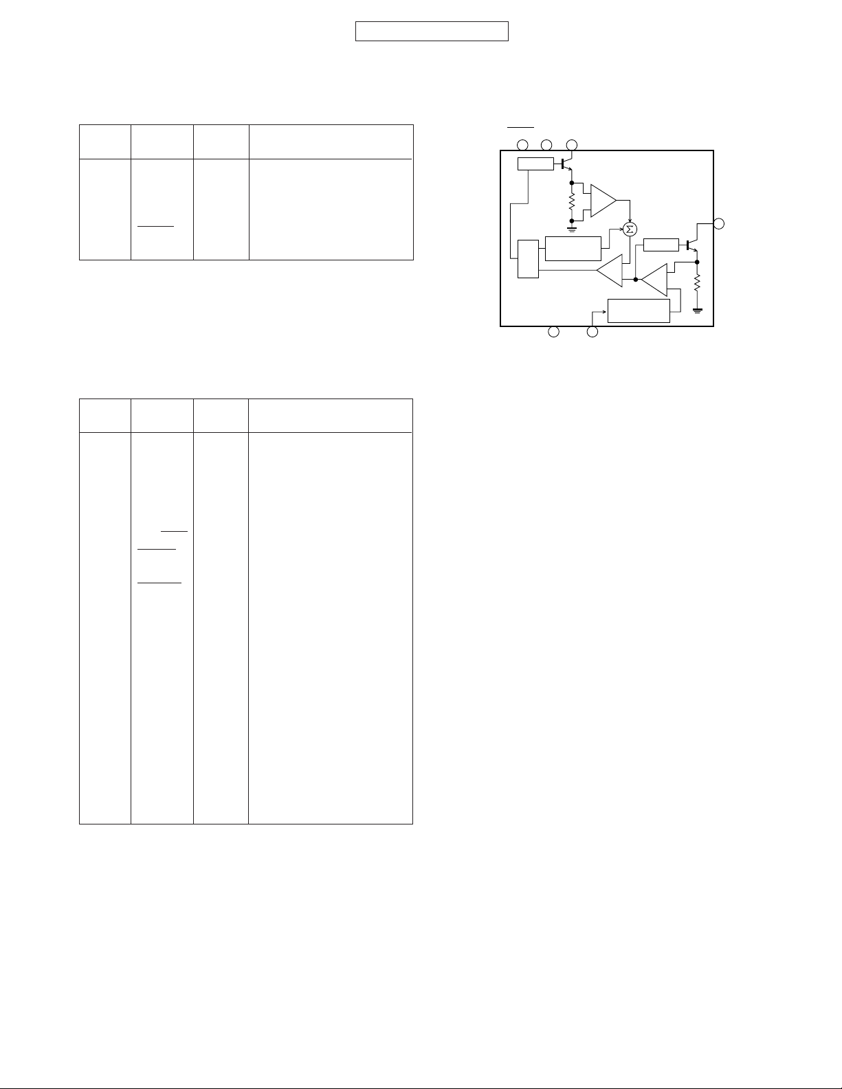
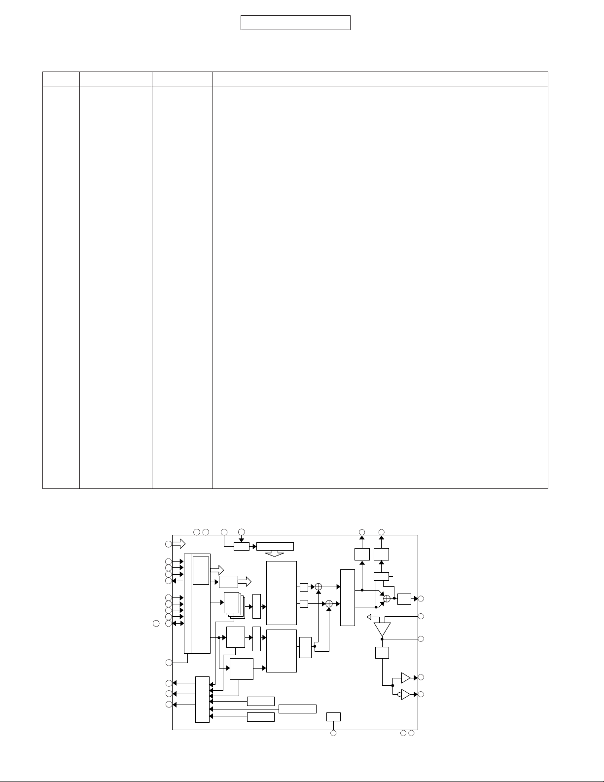
IC001 VHILT1932++-1R (LT1932): DC - DC
Pin No.
Terminal Input/
name Output
Description of terminal
1 SW Output LED voltage output
5 6 1
DRIVER
2 GND – Ground
3 LED – LED ground
4 RSET Input LED current setting
5 SHDN Input Chip enable
6 VIN Input Input
Q
IC002 VHIADM8830+-1L (ADM8830): CHARGE PUMP REGULATOR
Pin No.
Terminal Input/
name Output
1 VCC Input
Description of terminal
Positive supply voltage input
2 VOUT Output Voltage doubler output
3 LDO_IN Input Voltage regulator input
4
+5 VOUT
Output +5.1 V output pin
5 +5 VIN Input +5.1 V input pin
6 LDO_ Input Control logic input
ON/OFF
7 SHDN Input Digital input
8 SCAN/ Input Drive mode input
BLANK
9 CLKIN Input External clock input
10 +15 V Output +15.3 V output pin
OUT
11 C3– Input External capacitor
12 C3+ Input External capacitor
13 C2– Input External capacitor
14 C2+ Input External capacitor
15 C4– Input External capacitor
16 C4+ Input External capacitor
17 –10 V Output –10.2 V output pin
OUT
18 GND – Devide ground pin
19 C1– Input External capacitor
20 C1+ Input External capacitor
SWVINSHDN
1.2MHz
S
OSCILLATOR
R
GND RSET
Q1
+
x5
+
+
A2
-
LED CURRENT
REFERENCE
42
+
DRIVER
A1
GX10
3
LED
Q2
-
+
6 – 1
Page 2
GX10
CONFIDENTIAL
IC003 VHIADD8502+-1L (ADD8502): GRAYSCALE GENERATOR
Pin No.
Terminal Input/
name Output
Description of terminal
1 VL – Power supply (logic)
2 DIN Input Serial data
3 SCK Input Serial clock
4 CS-LD Input Load
5 CM Input Logic control
6 CV4 Input Logic control V4
7 REV1 Input Logic control 1
8 NC – Not used
9 NC – Not used
10 COM Output Common output
11 COM_M Input Common system Vref
12 NC – Not used
13 GND – Ground
14 V4 Output V4 voltage
15 V3 Output V3 voltage
16 V2 Output V2 voltage
17 V1 Output V1 voltage
18 V0 Output V0 voltage
19 VDD – Power supply
20 NC – Not used
21 REV2 Input Ref output select
22 GS2 Input Power save select 2
23 GS1 Input Power save select 1
24 PSK Input Power down
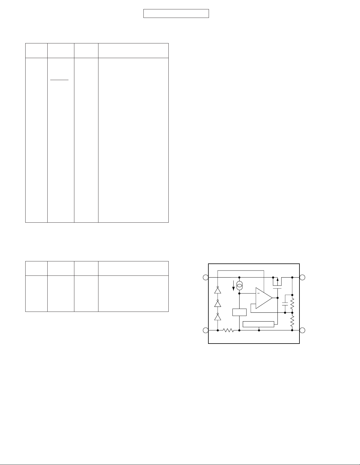
IC004 RH-IX2933AFZZL (IX2933AF): REGULATOR
Pin No.
In this unit, the terminal with asterisk mark (*) is (open) terminal which is not connected to the outside.
Terminal Input/
name Output
Description of terminal
1 VOUT Output Output
2 GND – Ground
3 VDD Input Input
4 CE Input Chip enable
5* NC – Not used
VDD
CE
3
+
VREF
CURRENT LIMIT
4
1
2
VOUT
GND
6 – 2
Page 3

CONFIDENTIAL
IC005 (LR38821A): TFT DISPLAY CONTROLLER (1/3)
Pin No.
In this unit, the terminal with asterisk mark (*) is (open) terminal which is not connected to the outside.
Terminal name
1 Dummy4 Input/Output Not used
2* NC – Not used
3 GND – Ground
4* NC – Not used
5 GND – Ground
6 VDD CORE – Power supply
7 PWM Output PWM output signal
8* NC – Not used
9 NCS Input Device select signal
10 VDD IO – Power supply
11 Dummy3 – Not used
12 VDD IO – Power supply
13* NC – Not used
14 B5 Output LCD panel B output signal
15 B4 Output LCD panel B output signal
16 B3 Output LCD panel B output signal
17 GND – Ground
18 TEST1 Input Test terminal
19 TEST SCMD Input Test terminal
20 NWR Input Host write strobe signal
21* NC – Not used
22* NC – Not used
23 B2 Output LCD panel B output signal
24 B1 Output LCD panel B output signal
25 B0 Output LCD panel B output signal
26 LS Output Data transmission signal
27* XOUT Output Oscillating circuit output
28 VDD IO – Power supply
29 GND – Ground
30 TST SCEN Input T est terminal
31 NRD Input Host read strobe signal
32 RS Input Register select signal
33 GND – Ground
34 DCLK Output Data sampling clock (display clock)
35 GS2 Output Gray scale switch signal
36 GS1 Output Gray scale switch signal
37 PS2 Output Power save signal (for source driver)
38 XIN Input Oscillating circuit input/external clock input signal
39* NC – Not used
40 NRES Input Master reset
41* NC – Not used
42* NC – Not used
43* NC – Not used
44 DB0 Input/Output Data bus
45 PS1 Output Power save signal (for source driver)
46 G5 Output LCD panel G output signal
47 G4 Output LCD panel G output signal
48 G3 Output LCD panel G output signal
49 DB1 Input/Output Data bus
50 DB2 Input/Output Data bus
51 DB3 Input/Output Data bus
52 DB4 Input/Output Data bus
53 VDD CORE – Power supply
54 GND – Ground
55 VDD IO – Power supply
56 G2 Output LCD panel G output signal
Input/Output
Description of terminal
GX10
6 – 3
Page 4

GX10
CONFIDENTIAL
IC005 (LR38821A): TFT DISPLAY CONTROLLER (2/3)
Pin No.
In this unit, the terminal with asterisk mark (*) is (open) terminal which is not connected to the outside.
Terminal name
57 DB5 Input/Output Data bus
58 VDD IO – Power supply
59 GND – Ground
60 VDD CORE – Power supply
61 G1 Output LCD panel G output signal
62 G0 Output LCD panel G output signal
63 R5 Output LCD panel R output signal
64 R4 Output LCD panel R output signal
65 DB6 Input/Output Data bus
66 DB7 Input/Output Data bus
67 DB8 Input/Output Data bus
68 DB9 Input/Output Data bus
69 R3 Output LCD panel R output signal
70 R2 Output LCD panel R output signal
71 R1 Output LCD panel R output signal
72* R0 Output LCD panel R output signal
73* PSD Output Power save signal (for power IC)
74 ECK Output Power save signal (for power IC)
75 CV4 Output Power save signal (for gray scale IC)
76 SE_DI Input Data input for four-wire serial IF
77 DB10 Input/Output Data bus
78 DB11 Input/Output Data bus
79 DB12 Input/Output Data bus
80* BNC Input Synchronous/asynchronous bus switch signal
81 GND – Ground
82 GSP Output Gate start signal
83 GMODE Output Gate output switch signal
84 SHD Output Power IC ON/OFF control terminal
85 VDD IO – Power supply
86 REV1 Output Polarity reverse control signal
87 SE_DO Output Data output for three-wire/four-wire serial IF
88 DB13 Input/Output Data bus
89 DB14 Input/Output Data bus
90 DB15 Input/Output Data bus
91* NC – Not used
92* NC – Not used
93 SPL Output Sampling start signal
94 ALW Output Write all mode switch signal
95 GCS1 Output Vertical scan start position setting signal
96 GND – Ground
97 REV2 Output Polarity reverse control signal
98 SE_CK Output Control clock for three-wire/four-wire serial IF
99* SE_LD2 Output Load signal for four-wire serial IF
100* NC – Not used
101 VDD IO – Power supply
102 Dummy2 – Not used
103 VDD IO – Power supply
104* NC – Not used
105 GCK Output Gate shift clock
106 GCS2 Output Vertical scan start position setting signal
107 VDD CORE – Power supply
108 PSK Output Power save signal (for gray scale IC)
109 SE_LD1 Output Load signal for three-wire serial IF
110 GND – Ground
11 1* NC – Not used
112 Dummy1 – Not used
Input/Output
Description of terminal
6 – 4
Page 5
CONFIDENTIAL
IC005 (LR38821A): TFT DISPLAY CONTROLLER (3/3)
109110111112
99101 100
SE_LD
2
DB13
VDD
IO
DB2
NC
313233
NRD
NCS NC
SE_LD
1
K
SE_DOREV1
SE_DIDB10
65666768
DB6DB7DB8
57585960
DB5
49505152
DB1
NC
TST
SCEN
SCMD
VDD
PSKGND NC
CORE
9798
REV2SE_C
GND GCS1 ALW SPL
VDD
IO
ECK
CV4
BNC
394041424344
NRES
NC PS2
2930
VDD
GND
IO
GND
TEST1NWR TEST
VDD
PWM
CORE
GCS2
GCK
GMODE
SHD
737475767778
PSD R0 R1
XIN
XOUT
B3
GND NC
Dummy
1
VDD
IO
DB15
79
DB12
DB9
CORE
DB4
DB0
GND
NC
Dummy
3
NC
NC
DB14
DB11
GNDVDD
DB3
NC
RS
NC
VDD
IO
103104105106107108
VDD
IO
NC
8182838487 8586888990
R2
R5
VDD
G2 GND
IO
G3
GS1 GS2 DCLK
B1
B0LS
B5
B4
NC VDD
GND NC
102
Dummy
2
919293949596
NC
80
BNCGNDGSP
69707172
R3
61626364
G1G0R4
53545556
VDD
CORE
45464748
PS1G5G4
3435363738
232425262728
B2
1213141516171819202122
IO
1234567891011
Dummy
4
1234567891011
GX10
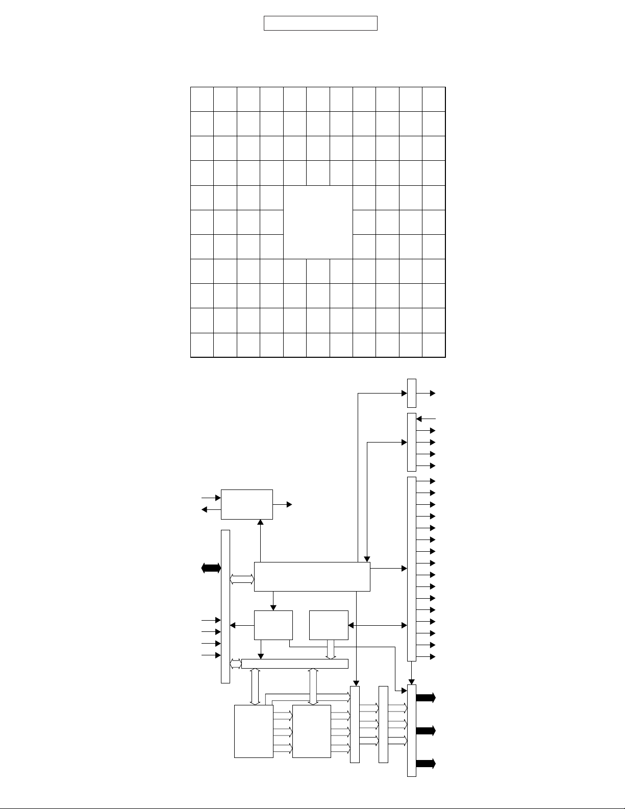
L
K
J
H
G
F
E
D
C
B
A
XIN
XOUT
DB[15:0]
RS
NRD
NWR
NCS
Clock Generator
HOST Interface
Controller
Master Clock (MCK)
Register
Bas
Memory Interface
Address
Generator
PWM
PWM
SE_DI
SE_DO
SE_LD1
SIOLCD Panel Interface
SE_LD2
SE_CK
DCLK
LS
SPL
PS[2:1]
GCK
GSP
REV[2:1]
GCS[2:1]
GS[2:1]
GMODE
Timing Generator
ALW
PSK
CV4
PSD
ECK
SHD
Display
Memory
Color
Palatte
6 – 5
Selector
CDE
R[5:0]
G[5:0]
B[5:0]
Page 6
GX10
CONFIDENTIAL
IC101 VHINJ287130-1L (NJM2871F03): 3.0 V REGULATOR
Pin No.
Terminal Input/
name Output
Description of terminal
1 CONT Input Control
2 GND – Ground
3N
B
– Noise bypass
4 VOUT Output Output
5 VIN Input Input
VIN
CONT
GND
5
Thermal
1
Bandgap
Reference
2
Protection
IC102 (AD6521ACA): ANALOG BASEBAND (1/2)
Pin No.
In this unit, the terminal with asterisk mark (*) is (open) terminal which is not connected to the outside.
Terminal name
Input/Output
Description of terminal
1 DVDD1 – Digital core power supply (1.6V AVDD1/2).
2 DGND1 – Digital ground.
3* IDACREF Output Current DAC bias resistor connection, rset.
4 AUXADC4 Input Auxiliary A/D converter input 4. (MVBAT)
5 AUXADC2 Input Auxiliary A/D converter input 2. (Camera thermal sensor)
6 AUXADC1 Input Auxiliary A/D converter input 1. (Jack detection)
7 REFOUT Input/Output Buffered reference output/external bias voltage input.
8 REFCAP Output Reference filter capacitor connection.
9 AVDD2 – Auxiliary analog power supply (2.4V to 2.6V).
10 AFCDAC Output Automatic frequency control signal output.
11 TDO Output Test data output.
12 TDI Input Test data input.
13 AGND4 – Analog substrate ground.
14* IDACOUT Output Current DAC output for battery charging.
15 AUXADC3 Input Auxiliary A/D converter Input 3. (Battery sense)
16 AUXADC5 Input Auxiliary A/D converter Input 5. (Battery thermal sensor)
17 AUXADC6 Input Auxiliary A/D converter Input 6.
18 AGND2 – Auxiliary analog ground.
19*
NC (REFCAP2)
Output Reserved for reference filter capacitor.
20 QRXN Input Differential analog input for quadrature receive signal.
21 TCK Input Test clock.
22 TMS Input Test mode select.
23 QTXN Output Differential analog output for quadrature transmit signal.
24 QRXP Input Differential analog input for quadrature receive signal.
25 VSDO Output Voiceband serial port data output.
26 VSFS Output Voiceband serial port input/output framing signal.
27 QTXP Output Differential analog output for quadrature transmit signal.
28 IRXN Input Differential analog input for in-phase receive signal.
29 VSDI Input Voiceband serial port data input.
30 BSOFS Output Baseband serial port output framing signal.
31 ITXN Output Differential analog output for in-phase transmit signal.
32 IRXP Input Differential analog input for in-phase receive signal.
33 BSDO Output Baseband serial port data output.
34 BSIFS Output Baseband serial port input framing signal.
35 ITXP Output Differential analog output for in-phase transmit signal.
36 AVDD1 – Baseband Analog Power Supply (2.4V to 2.6V).
37 DVDD2 – Digital Interface Power Supply
(The greater of DVDD1 or DVDD3 or AVDD3-0.2V, to maximum 3.3V).
38 BSDI Input Baseband serial port data input.
39 AGND1 – Baseband analog ground.
40 VINAUXN Input Differential voiceband auxiliary input.
41 ASDI Input Auxiliary serial port data input.
42 ASFS Input Auxiliary serial port input/output framing signal.
4
VOUT
3
NB
6 – 6
Page 7

CONFIDENTIAL
IC102 (AD6521ACA): ANALOG BASEBAND (2/2)
Pin No.
In this unit, the terminal with asterisk mark (*) is (open) terminal which is not connected to the outside.
Terminal name
43 RAMPDAC Output Power ramping control signal output.
44 VINAUXP Input Differential voiceband auxiliary input. (Jack mic audio input)
45 ASDO Output Auxiliary serial port data output.
46 MCLK Input Master clock input.
47 ARSM Input Advance baseband receive state machine.
48 RXON Input Baseband receive section power-on input.
49 DGND3 – Digital ground.
50c BUZZER Output Buzzer output.
51 AGND3 – Voiceband analog ground.
52 AVDD3 – Voiceband analog power supply (2.4 V to 2.7 V).
53* NC (MICCAP) Output Reserved for microphone.
54 VINNORP Input Differential voiceband normal input. (Mic audio input)
55 RESET Input Active low reset signal input.
56 MCLKEN Output Master clock enable.
57 ATSM Input Advance baseband transmit state machine.
58 TXON Input Baseband transmit section power-on input.
59 DVDD3 – Digital core power supply (1.6 V to AVDD1/2).
60 VOUTAUXN Output Differential voiceband auxiliary output.
61 VOUTNORN Output Differential voiceband normal output. (Earpiece audio output)
62 VOUTNORP Output Differential voiceband normal output. (Earpiece audio output)
63 VOUTAUXP Output Differential voiceband auxiliary output. (Jack Earpiece audio output)
64 VINNORN Input Differential voiceband normal input.
Input/Output
Description of terminal
GX10
6 – 7
Page 8
GX10
CONFIDENTIAL
IC103 VHIYMU759B+-1L (YMU759B): SOUND
Pin No.
In this unit, the terminal with asterisk mark (*) is (open) terminal which is not connected to the outside.
Terminal name
Input/Output
Description of terminal
1 CLKI Input Clock input terminal (2 – 20 MHz)
2 EXT1 Output External control terminal 1
3 /IRQ Output Interrupt output terminal
4 /RST Input Hardware reset input terminal
5 IFSEL Input CPU I/F select; L: serial I/F, H: parallel I/F
6 PLLC – Built-in PLL capacitor terminal
7 VDD – Power supply
8 VSS – Ground
9 VREF – Analog reference voltage terminal
10*
HPOUT-L/MONO
Output Headphone output Lch
11* HPOUT-R Output Headphone output Rch
12 EQ1 – Equalizer terminal 1
13 EQ2 – Equalizer terminal 2
14 EQ3 – Equalizer terminal 3
15 SPVDD – Analog power supply for speaker amplifier (Typ + 3.6 V)
16 SPVSS – Analog ground for speaker amplifier
17 SPOUT1 Output Speaker terminal 1
18 SPOUT2 Output Speaker terminal 2
19 EXT2 Output External control terminal 2
20 D7 Input/Output Parallel I/F data bus 7
21 D6 Input/Output Parallel I/F data bus 6
22 D5 Input/Output Parallel I/F data bus 5
23 D4 Input/Output Parallel I/F data bus 4 (Not connected when IFSEL terminal at L)
24 D3 Input/Output Parallel I/F data bus 3 (Not connected when IFSEL terminal at L)
25 D2 Input/Output Parallel I/F data bus 2 (Not connected when IFSEL terminal at L)
26 D1 Input/Output Parallel I/F data bus 1 (Not connected when IFSEL terminal at L)
27 D0 Input/Output Parallel I/F data bus 0 (Not connected when IFSEL terminal at L)
28 /WR Input Parallel I/F write pulse (Not connected when IFSEL terminal at L)
29 SDIN (/CS) Input IFSEL terminal = L serial I/F data input
IFSEL terminal = H parallel I/F chip select input
30 SYNC (A0) Input IFSEL terminal = L serial I/F data read signal
FSEL terminal = H parallel I/F address signal
31 SCLK (/RD) Input IFSEL terminal = L serial I/F bit clock input
IFSEL terminal = H parallel I/F read pulse
32* SDOUT Output Serial I/F data output (external pull-up resistor required)
HPOUT-L/
HPOUT-R
Vol R
VREF
11
HP
MONO
10
HP
Vol L
Select Mono
+-
SP
Vol
EQ
Vol
16 159
SPVSS
SPVDD
12
13
14
17
18
EQ1
EQ2
EQ3
SPOUT1
SPOUT2
/RST
SCLK
SYNC
SDIN
SDOUT
/WR
20 ~ 27
D0~D7
IFSEL
/IRQ
EXT1
EXT2
PLLC
687
Register
FM
FIFO
x1
ADPCM
CLKI
1
PLL
Seq
FIFO
ADPCM
Waveform
FIFO
Timing Generator
Sequencer
(Fs = 49.7 kHz)
Sequencer
(Fs = 4 or 8 kHz)
LED control
TIMER
FM
Synthesizer
Number of
voices: 16
ADPCM
Playback
Vibrator control
Vol
Vol
LPF
Rch
16-bit
Lch
DAC
Vol
&
VREF
VREF
VDD
VSS
4
31
Power
30
Down
29
Control
32
SELECT
29
/CS
30
A0
28
CPU I/F
31
/RD
5
3
2
19
Mix & Select
6 – 8
Page 9

CONFIDENTIAL
IC104 (AD6526XCA): DIGITAL BASEBAND (1/3)
Pin
Terminal
No. Name Name
1 A1 GPO05 Output ARMSM
2 A2 VDDRTC – RTC power supply 1.8 V
3 A3 OSCIN Input 32.768 kHz crystal input - inverted (GND if no crystal)
4 A4 KEYPADCOL3 Output Key matrix (COL3)
5 A5 KEYPADROW4 Input Key matrix (ROW4)
6 A6 KEYPADROW0 Input Key matrix (ROW0)
7 A7 GPO22 Output Back light control
8 A8 GPIO15 Output Sub-screen display RAM select
9 A9 GPIO13 Input Charge detect
10 A10 GPIO09 Output IrDA power ON
11 A11 GPIO06 Input Camera INT
12 A12 GND09 – Ground (7 periphery and 4 core)
13 A13 USC3 Input USC pin (ADP detect)
14 A14 USC2 Output USC pin (TXD)
15 B1 GPO00 Output Receiver on RxOn
16 B2 PWRON Output Power on/off control
17 B3 OSCOUT Output 32.768 kHz oscillator output and feedback to crystal
18 B4 KEYPADCOL2 Output Key matrix (COL2)
19 B5 KEYPADROW3 Input Key matrix (ROW3)
20 B6 GND11 – Ground (7 periphery and 4 core)
21 B7 GPIO17 Output Sub-screen display data output
22 B8 GPIO14 Output Sub-screen display serial clock
23 B9 GPIO12 Output Reset (sound)
24 B10 VEXT2 – External device power supply 3 V
25 B11 GPIO05 Input IRQ (sound)
26 B12 GPIO02 Output Camera reset
27 B13 USC6 Input USC pin (CONT2)
28 B14 VEXT1 – External device power supply 3 V
29 C1 GPO06 Output ATSM
30 C2 GPO01 Output Tx on
31 C3 KEYPADCOL4 Output Key matrix (COL4)
32 C4 KEYPADCOL0 Output Key matrix (COL0)
33* C5 GPO23 Input/Output (Not used)
34 C6 VEXT3 – External device power supply 3 V
35 C7 GPIO11 Output Flash memory write protect
36 C8 VCC4 – Core power supply voltage 1.8 V
37 C9 GPIO10 Output Flash memory Vpp
38 C10 GPIO07 Output Camera power on
39 C11 GPIO03 Output IrDA TXD
40 C12 USC5 Output USC pin (CTS)
41 C13 GND08 – Ground (7 periphery and 4 core)
42 C14 USC0 Input USC pin (ADP)
43 D1 CLKOUT Output 13 MHz clock output
44 D2 CLKOUTGATE Input Hardware CLKOUT on/off Switching
45 D3 VSSRTC – RTC power supply return (Ground)
46 D4 KEYPADROW2 Input Key matrix (ROW2)
47 D5 VEXT4 – External device power supply 3 V
48 D6 GPIO16 Output Sub-screen display chip select
49 D7 GND10 – Ground (7 periphery and 4 core)
50 D8 GPIO08 Input (CONT1)
51 D9 GPIO04 Input Flip SW detection
52 D10 GPIO01 Input IrDA RXD
53 D11 GPIO00 Output Screen display reset
54 D12 USC1 Input USC pin (RXD)
55 D13 GPO20 Output Sirial data (RF)
56 D14 GPO19 Output A0 (sound)
In this unit, the terminal with asterisk mark (*) is (open) terminal which is not connected to the outside.
Signal
Input/Output
Function
GX10
6 – 9
Page 10

GX10
CONFIDENTIAL
IC104 (AD6526XCA): DIGITAL BASEBAND (2/3)
Pin
Terminal
No. Name Name
57 E1 GPO24 Output Reset output analog baseband RESET
58 E2 ASDI Input Auxiliary serial port data input
59 E3 VPEG1 – AD6521 interface power supply 2.8 V
60 E4 KEYPADCOL1 Output Key matrix (COL1)
61 E11 USC4 Output USC pin out (RTS)
62 E12 GPO18 Output Enable (RF)
63 E13 GPO16 Output
64 E14 GPO11 Output Back light SW
65 F1 ASDO Output Auxiliary serial port data output
66 F2 ASFS Output Auxiliary serial port framing signal
67 F3 BSDO Output Baseband serial port data output
68 F4 KEYPADROW1 Input Key matrix (ROW1)
69 F11 GPO21 Output Serial clock (RF)
70* F12 GPO10 Output (Not used)
71 F13 GPO08 Output Camera A18
72 F14 GPO07 Output Charge enable
73 G1 BSIFS Output Baseband serial port input framing signal
74 G2 BSDI Input Baseband serial port data input
75 G3 VSDI Input Voiceband serial port data input
76 G4 BSOFS Output Baseband serial port output framing signal
77 G11 GPO17 Output DCS SEL (BS1)
78 G12 GPO03 Output Audio bias control
79 G13 GPO02 Output PCS SEL (BS2)
80 G14 CLKON Output Oscillator power control signal (on/off)
81 H1 VCC1 – Core power supply voltage 1.8 V
82 H2 VSFS Output Voiceband serial port framing signal
83 H3 VSDO Output Voiceband serial port data output
84 H4 ADD00 Output Processor address bus
85 H11 GPO09 Output RF enable
86 H12 GPO04 Output Key back light control
87 H13 GPIO19 Input JTAG test mode select (TMS)
88 H14 GPIO18 Output JTAG test clock (TCK)
89 J1 GND01 – Ground (7 periphery and 4 core)
90 J2 ADD02 Output Processor address bus
91 J3 ADD01 Output Processor address bus
92 J4 ADD03 Output Processor address bus
93 J11 GPIO21 Output JTAG test data output (TDO)
94 J12 GPIO20 Input JTAG test data input (TDI)
95 J13 SIMDATAOP Input/Output SIM data output/input
96 J14 GPIO22 Input End of charge
97 K1 GND02 – Ground (7 periphery and 4 core)
98 K2 ADD05 Output Processor address bus
99 K3 ADD04 Output Processor address bus
100 K4 ADD06 Output Processor address bus
101 K11 JTAGEN Input JTAG enable
102 K12 SIMCLK Output SIM clock
103 K13 GPIO24 Output SIM supply enable
104 K14 VCC3 – Core power supply voltage 1.8 V
105 L1 ADD08 Output Processor address bus
106 L2 VMEM1 –
107 L3 ADD09 Output Processor address bus
108 L4 ADD07 Output Processor address bus
109 L5 ADD10 Output Processor address bus
110 L6 GND04 – Ground (7 periphery and 4 core)
111 L7 DATA05 Input/Output Processor data bus
112 L8 GND05 – Ground (7 periphery and 4 core)
Signal
Input/Output
Function
GSM SEL (BS0)
Memory power supply 3 V
In this unit, the terminal with asterisk mark (*) is (open) terminal which is not connected to the outside.
6 – 10
Page 11

CONFIDENTIAL
IC104 (AD6526XCA): DIGITAL BASEBAND (3/3)
Pin
Terminal
No. Name Name
113 L9 VSIM – SIM power supply 2.8 V
114 L10 GPIO23 Output SIM reset
115 L11 GND07 – Ground (7 periphery and 4 core)
116 L12 CLKIN Input 13 MHz system clock input (Auto Detect)
117 L13 nGPCS1 Output 16M bit flash chip select
118* L14 GPIO32 Input (Not used)
119 M1 ADD11 Output Processor address bus
120 M2 ADD12 Output Processor address bus
121 M3 ADD18 Output Processor address bus
122 M4 ADD21 Output Processor address bus
123 M5 nDISPLAYCS Input/Output 4 M bit SRAM/sound/screen display controler chip select
124 M6 DATA02 Input/Output Processor data bus
125 M7 DATA04 Input/Output Processor data bus
126 M8 DATA08 Input/Output Processor data bus
127 M9 DATA10 Input/Output Processor data bus
128 M10 DATA13 Input/Output Processor data bus
129 M11 nRD Input/Output Processor read strobe
130 M12 nGPCS0 Output Camera chip select
131 M13 nROMCS Output 64 M bit flash chip select
132 M14 nRAMCS Output 16 M bit PSRAM chip select
133 N1 ADD13 Output Processor address bus
134 N2 ADD15 Output Processor address bus
135 N3 ADD17 Output Processor address bus
136 N4 ADD20 Output Processor address bus
137 N5 VMEM2 –
138 N6 DATA00 Input/Output Processor data bus
139 N7 DATA03 Input/Output Processor data bus
140 N8 DATA07 Input/Output Processor data bus
141 N9 VMEM3 –
142 N10 DATA12 Input/Output Processor data bus
143 N11 DATA15 Input/Output Processor data bus
144 N12 nHWR Output Processor high write strobe
145 N13 VMEM4 –
146 N14 nRESET Input System reset input
147 P1 ADD14 Output Processor address bus
148 P2 ADD16 Output Processor address bus
149 P3 GND03 – Ground (7 periphery and 4 core)
150 P4 ADD19 Output Processor address bus
151 P5 ADD22 Output Processor address bus
152 P6 DATA01 Input/Output Processor data bus
153 P7 VCC2 – Core power supply voltage 1.8 V
154 P8 DATA06 Input/Output Processor data bus
155 P9 DATA09 Input/Output Processor data bus
156 P10 DATA11 Input/Output Processor data bus
157 P11 DATA14 Input/Output Processor data bus
158 P12 GND06 – Ground (7 periphery and 4 core)
159 P13 nLWR Output Processor low write strobe
160 P14 nWE Output Processor write strobe (nWR)
In this unit, the terminal with asterisk mark (*) is (open) terminal which is not connected to the outside.
Signal
Input/Output
Function
Memory power supply 3 V
Memory power supply 3 V
Memory power supply 3 V
GX10
6 – 11
Page 12
GX10
CONFIDENTIAL
IC105, IC307 VHILM20BIM7-1L (LM20BIM7): TEMPERATURE SENSOR
Pin No.
In this unit, the terminal with asterisk mark (*) is (open) terminal which is not connected to the outside.
Terminal Input/
name Output
Description of terminal
1* NC – Not used
2 GND – Ground
3 VO Output Output
4 V+ Input Input
5 GND – Ground
(TOP VIEW)
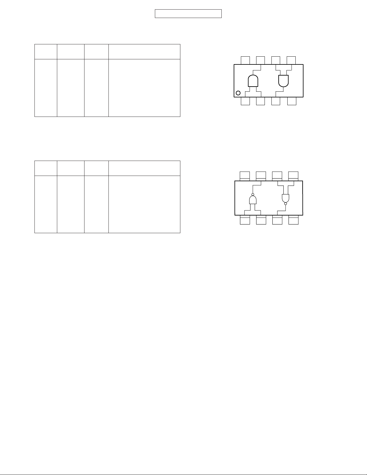
IC107, IC108, IC110 VHITC7SZ32A-1L (TC7SZ32AFE): LOGIC
Pin No.
Terminal Input/
name Output
Description of terminal
1 A Input Input
2 B Input Input
3 GND – Ground
4 Y Output Output
5 VCC – Power supply
(TOP VIEW)
13542
13542
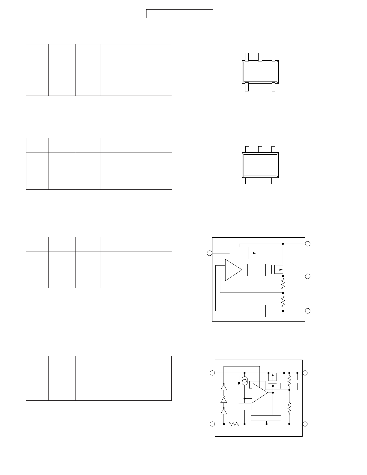
IC201 VHIXC620925-1L (XC6209B252MR): HIGH SPEED LDO REGULATOR
IC306 VHIXC620439-1L (XC6204B392MR): HIGH SPEED LDO REGULATOR
Pin No.
In this unit, the terminal with asterisk mark (*) is (open) terminal which is not connected to the outside.
Terminal Input/
name Output
Description of terminal
1 VIN Input Input
2 VSS – Ground
3 CE Input Chip enable
4* NC – Not used
5 VOUT Output Output
CE
3
ON/OFF
Control
+
Each ciruit
Current
Limit
Voltage
Reference
IC203 VHIRQ5RW18B-1L (RQ5RW18B): 1.8 V REGULATOR
Pin No.
Terminal Input/
name Output
Description of terminal
1 GND – Ground
2 VDD – Power supply
3 VOUT Output Output
4 CE Input Chip enable
VDD
2
+
-
VREF
3
1
5
2
VOUT
VIN
VOUT
VSS
6 – 12
CE
4
CURRENT LIMIT
1
GND
Page 13
CONFIDENTIAL
+
-
1
2
3
CE
VSS
VIN
ON/OFF
Control
Current
Limit
Voltage
Reference
Each ciruit
5
VOUT
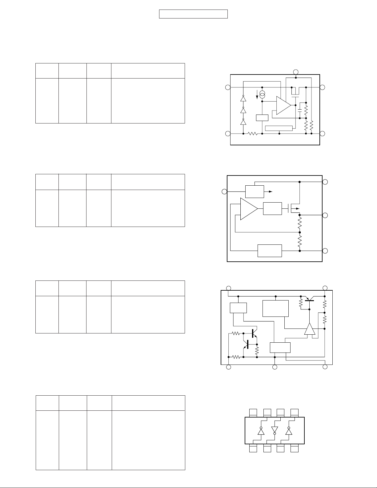
IC205 VHIR116030B-1L (R1160N301B): REGULATOR
IC302 VHIR116030B-1L (R1160N301B): REGULATOR
[Refer to the“Schematic diagram”on page 5 - 24.]
Pin No.
IC302 VHIXC620930-1L (XC6209B302MR): HIGH SPEED LDO REGULATOR
Pin No.
In this unit, the terminal with asterisk mark (*) is (open) terminal which is not connected to the outside.
Terminal Input/
name Output
Description of terminal
1 VDD Input Input
2 GND – Ground
3 CE Input Chip enable
4 ECO Input
High speed/low consumption
selector switch
5 VOUT Output Output
[Refer to the“Schematic diagram”on page 5 - 24.]
Terminal Input/
name Output
1 VIN Input Input
2 VSS – Ground
3 CE Input ON/OFF Control
4* NC – Not used
5 VOUT Output Output
Description of terminal
1
VDD
-
+
VREF
3
CE GND
CURRENT LIMIT
ECO
GX10
4
VOUT
5
2
IC206 VHITK11131C-1R (TK11131C): REGULATOR
-+
VOUT
4
3
NP
Pin No.
Terminal Input/
name Output
Description of terminal
1 CONT Input Control
2 GND – Ground
3 NP – Capacitor
4 VOUT Output Output
5 VIN Input Input
VIN
5
1
CONT
Control
Circuit
320 k
500 k
Over Heat &
Over Current
Protection
Bandgap
Reference
2
GND
IC301 VHITC7WH04K-1R (TC7WH04FK): LOGIC
Pin No.
Terminal Input/
name Output
1 1A Input Input 1
Description of terminal
2 3Y Output Output 3
3 2A Input Input 2
4 GND – Ground
5 2Y Output Output 2
6 3A Input Input 3
7 1Y Output Output 1
8 VCC – Power supply
VCC 1Y 3A 2Y
8765
1234
1A 3Y 2A GND
(TOP VIEW)
6 – 13
Page 14

GX10
CONFIDENTIAL
IC303, IC304 VHITK11129C-1R (TK11129CSIL): 2.9 V REGULATOR
Pin No.
Terminal Input/
name Output
Description of terminal
1 CONT Input Control
2 GND – Ground
3 NP – Capacitor
4 VOUT Output Output
5 VIN Input Input
VIN
5
Control
Circuit
500 k
Constant
Current
Source
Over Heat &
Over Current
Protection
Bandgap
Reference
VOUT
4
1
CONT
IC305 VHIR3111Q25-1L (R3111Q251C): VOLTAGE DETECTOR
Pin No.
TIn this unit, the terminal with asterisk mark (*) is (open) ter-
minal which is not connected to the outside.
Terminal Input/
name Output
Description of terminal
1 OUT Output Output
2 VDD – Power supply
3* NC – Not used
4 VSS – Ground
VSS
2
IC831 VHIPF08123B-1L (PF08123B): RF POWER AMP.
Pin No.
Terminal name
Input/Output
Description of terminal
1 Pin GSM Input Input power from TXVCO (GSM)
2 Vapc Input Power control voltage from APCIC
3 Vdd1 – Power supply
4 Pout GSM Output Output power (GSM)
5 Pout DCS Output Output power (DCS)
6 Vdd2 – Power supply
7 Vctl Input Band select switch
8 Pin DCS Input Input power from TXVCO (DCS)
9 GND – Ground
VREF
2
GND
3
NP
+
1
OUT
-
4
GND
Pin DCS
Pin GSM
Vctl
7
8
1
Bias circuit
23
Vapc
Vdd2
6
Vdd1
6 – 14
5
Pout DCS
Pout GSM
4
Page 15

CONFIDENTIAL
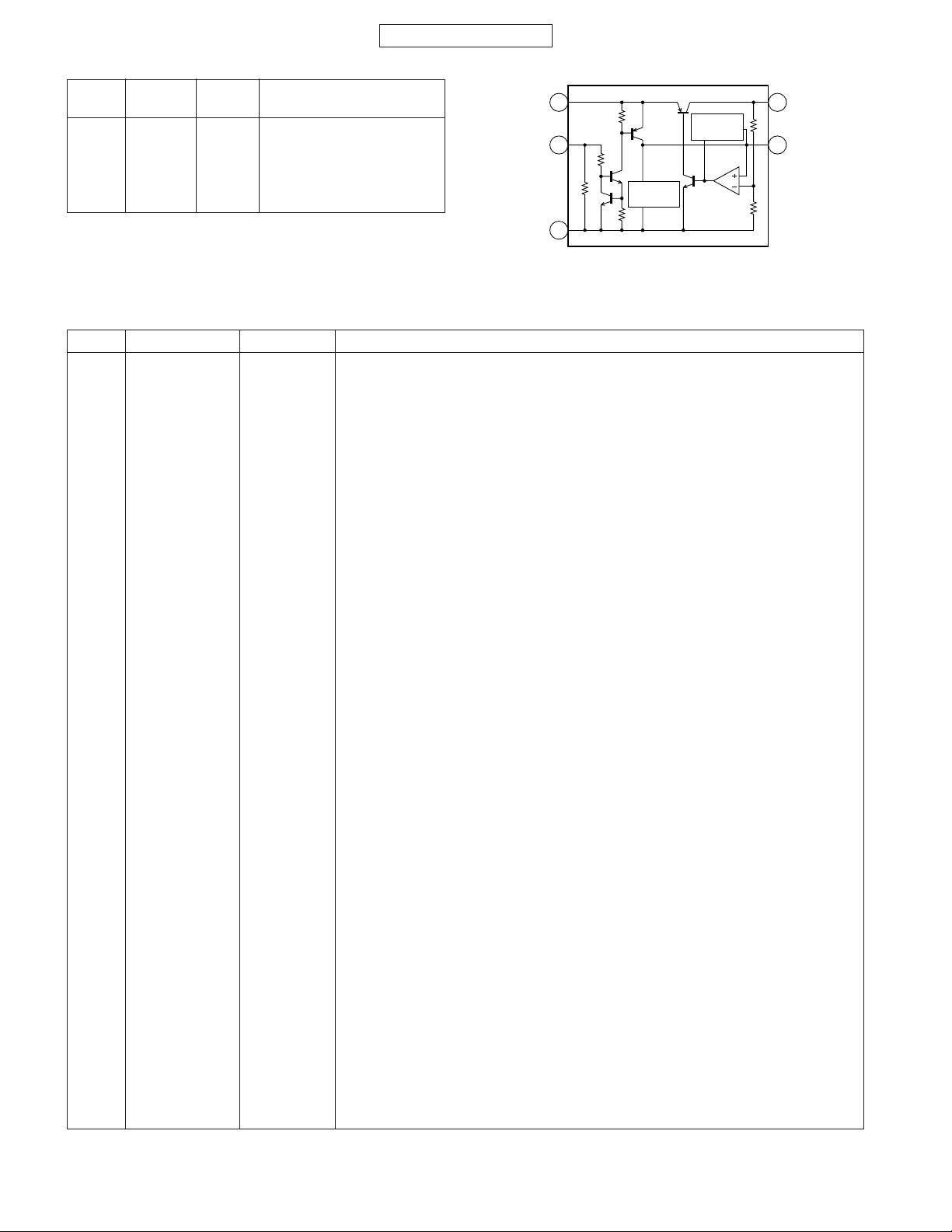
IC881 VHIHD155173-1L (HD155173): AUTO POWER CONTROL
Pin No.
Terminal name
1 VAPC1 Output APC voltage output terminal (GSM900)
2 IN1(-) Input Output amp negative terminal (GSM900)
3 IN(+) Input Output amp positive terminal
4 VCC1 Input Power supply
5 DACin Input DAC voltage input terminal
6 AMPIB Input DAC amp input terminal
7 AMPO Output DAC amp output terminal
8 Mode SW Input Mode switch
9 VCC2 Input Power supply
10 PS Input Power save switch
11 GND2 – Ground
12 RFin1 Input GSM900 signal input terminal
13 RFin2 Input DCS/PCS signal input terminal
14 GND1 – Ground
15 IN2(-) Input Output amp negative terminal (DCS/PCS)
16 VAPC2 Output APC voltage output terminal (DCS/PCS)
Input/Output
Description of terminal
GX10
6 – 15
Page 16

GX10
CONFIDENTIAL
IC901 VHIHD155148-1L (HD155148TF): RF
Pin No.
Terminal name
1 GNDLNA – Ground for LNA bias
2 VCCLNA Input VCC for LNA transistor and LNA bias
3
4 PCSLNAI Input Positive input for LNA transistor (PCS)
5 PCSLNAIB Input Negative input for LNA transistor (PCS)
6
7 DCSLNAI Input Positive input for LNA transistor (DCS)
8 DCSLNAIB Input Negative input for LNA transistor (DCS)
9
10 GSMLNAI Input Positive input for LNA transistor (GSM)
1 1 GSMLNAIB Input Negative input for LNA transistor (GSM)
12
13 VCCLNA Input VCC for LNA transistor and LNA bias
14 GNDOPLL – Ground for OPLL
15 VCOIN Input TXVCO signal input
16 VCCOPLL Input VCC for OPLL and phase comparator
17 PLLOUT Output Current output to control and modulate TXVCO
18
19
20 IINB Input Negative input of I signal for modulator
21 IIN Input Positive input of I signal for modulator
22 QINB Input Negative input of Q signal for modulator
23 QIN Input Positive input of Q signal for modulator
24 QOUTB Output Negative output of Q channel
25 QOUT Output Positive output of Q channel
26 IOUTB Output Negative output of I channel
27 IOUT Output Positive output of I channel
28 VCCIFVCO Input VCC for IFVCO and IFVCO buffer and divider
29 GNDIFVCO – Ground for IFVCO buffer an divider
30 VCCOSC Input VCC for IFVCO
31 TCXOCONT – TCXOOUT frequency (GND: 26 MHz/VCC: 13 MHz)
32 VCCIFSYN Input VCC for IF synthesizer and TCXOOUT buffer (13 MHz/26 MHz)
33 CPIFSYN Output Charge pump output of IF synthesizer
34 GNDIFSYN – Ground for IFsynthesizer and TCXOOUT buffer (13 MHz/26 MHz)
35 LE Input Load enable for serial data
36 TCXOOUT Output TCXO output for base band
37 CLK Input Clock for serial data
38 TCXOIN Input TCXO input for IF and RF synthesizer
39 SDATA Input Serial data
40 GNDRFSYN – Ground for RF synthesizer and TCXO input buffer (26 MHz)
41 VCCRFSYN Input VCC for RF synthesizer and TCXO input buffer (26 MHz)
42 BANDSW Output Band select or frequency select switch for RFVCO
43 FLOCK Output Fast lock control for RF synthesizer
44 CPRFSYN Output Charge pump output of RF synthesizer
45 GNDBB – Ground for base band
46 VCCBB Input VCC for base band
47 VCCRFLO Input VCC for RF local buffer and divider
48 GNDRFLO – Ground for RF local buffer and divider
49 RFLOINB Input Negative input for RF local
50 RFLOINB Input Positive input for RF local
51 GNDMIX – Ground for direct conversion mixer
52 CAPQB Output Capacitor for Q channel LPF (Negative output)
53 CAPQ Output Capacitor for Q channel LPF (Positive output)
54 CAPIB Output Capacitor for I channel LPF (Negative output)
55 CAPI Output Capacitor for I channel LPF (Positive output)
56 VCCMIX Input VCC for direct conversion mixer
GNDDUM,GNDPCS
GNDPCSB,GNDDCS
GNDDCSB,GNDGSM
GNDGSMB,GNDDUM
VCCIQ/ADDAC
GNDIQ/ADDAC
Input/Output
– Ground for emitter of LNA transistor (PCS)
– Ground for emitter of LNA transistor (PCS,DCS)
– Ground for emitter of LNA transistor (DCS,GSM)
– Ground for emitter of LNA transistor (GSM)
Input VCC for IQ modulator and offset canceling AD/DAC
– Ground for IQ modulator and offset canceling AD/DAC
Description of terminal
6 – 16
Page 17
CONFIDENTIAL
1234
8765
VCC 1Y 2B 2A
1A 1B
(TOP VIEW)
2Y GND
IC991, IC993 VHINL27WZ08-1R (NL27WZ08): LOGIC
Pin No.
IC992 VHITC7W00FK-1R (TC7W00FK): LOGIC
Pin No.
Terminal Input/
name Output
Description of terminal
1 1A Input Input 1
2 1B Input Input 1
3 2Y Output Output 2
4 GND – Ground
5 2A Input Input 2
6 2B Input Input 2
7 1Y Output Output 1
8 VCC – Power supply
Terminal Input/
name Output
Description of terminal
1 1A Input Input 1
2 1B Input Input 1
3 2Y Output Output 2
4 GND – Ground
5 2A Input Input 2
6 2B Input Input 2
7 1Y Output Output 1
8 VCC – Power supply
VCC
1Y 2B 2A
87645
1
23
1A
1B
2Y
GX10
GND
6 – 17
Page 18

GX10
— MEMO —
CONFIDENTIAL
6 – 18
Page 19

CONFIDENTIAL
PARTS GUIDE
DIGITAL MOBILE PHONE
MODEL GX10
(INTERNAL MODEL NAME:
E : For U.K. S : For Spain
F : For France H : For Netherlands
G : For Germany P : For Portugal
T : For Italy R : For Ireland
EP : For U.K. (Prepaid)
GX10
TQ-GX10E/F/G/T/S/H/P/R/EP)
“HOW TO ORDER REPLACEMENT PARTS”
To have your order filled promptly and correctly, please furnish the following information.
1.MODEL NUMBER2.REF. No. 3.PART NO.4.DESCRIPTION
MARK: NOT REPLACEMENT ITEM
Explanation of capacitors/resistors parts codes
Capacitors
VCC ....................... Ceramic type
VCK........................ Ceramic typ e
VCT........................ Semiconductor type
VC • • MF ............... Cylindrical type (without lead wire)
VC • • MN............... Cylindrical type (without lead wire)
VC • • TV................ Square type (without lead wire)
VC • • TQ ............... Square type (without lead wire)
VC • • CY ............... Square type (without lead wire)
VC • • CZ ............... Square t ype (without lead wi re)
VC • • • • • • • • • J .. The 13th character represents capacity difference.
("J" ±5%, "K" ±10%, "M" ±20%, "N" ±30%,
"C" ±0.25 pF, "D" ±0.5 pF, "Z" +80-20%.)
If there are no indications for the electrolytic capacitors, error is ±20%.
Resistors
VRD ....................... Carbon-film type
VRS........................ Carbon-film type
VRN ....................... Metal-film type
VR • • MF ............... Cylindrical type (without lead wire)
VR • • MN............... Cylindrical type (without lead wire)
VR • • TV................ Square type (without lead wire)
VR • • TQ ............... Square type (without lead wire)
VR • • CY ............... Square type (without lead wire)
VR • • CZ ............... Square type (w ithout lead wire)
VR • • • • • • • • • J .. The 13th character represents error.
("J" ±5%, "F" ±1%, "D" ±0.5%.)
If there are no indications for other parts, the resistors are ±5%
carbon-film type.
NOTE:
Parts marked with “ ” are important for maintaining the safety of the set.
Be sure to replace parts with specified ones for maintaining the safety and performance of the set.
Page 20

GX10
CONFIDENTIAL
PARTS CODE NO. PARTS CODE
DESCRIPTIONNO.
INTEGRATED CIRCUITS
IC001 VHILT1932++-1R DC-DC,LT1932
IC002 VHIADM8830+-1L Charge Pump Regulator,
IC003 VHIADD8502+-1L Grayscale Generator,ADD8502
IC004 RH-IX2933AFZZL Regulator,IX2933AF
IC005 ———— Not Replacement Item,This parts
IC101 VHINJ287130-1L 3.0V Regulator,NJM2871F03
IC102 ———— Not Replacement Item,This parts
IC103 VHIYMU759B+-1L Sound,YMU759B
IC104 ———— Not Replacement Item,This parts
IC105 VHILM20BIM7-1L Temperature Sensor,LM20BIM7
IC106 ———— Not Replacement Item,This parts
IC107,108 VHITC7SZ32A-1L Logic,TC7SZ32AFE
IC110 VHITC7SZ32A-1L
IC201 VHIXC620925-1L High Speed LDO Regulator,
IC202 VHIAD340818-1L Power Supply,ADP3408ACP
IC203 VHIRQ5RW18B-1L
IC205 VHIR116030B-1L Regulator,R1160N301B
IC206 VHITK11131C-1R Regulator,TK11131C
IC301 VHITC7WH04K-1R Logic,TC7WH04FK
IC302 VHIR116030B-1L Regulator,R1160N301B
or
VHIXC620930-1L High Speed LDO Regulator,
IC303,304 VHITK11129C-1R 2.9V Regulator,TK11129CSIL
IC305 VHIR3111Q25-1L Voltage Detector,R3111Q251C
IC306 VHIXC620439-1L High Speed LDO Regulator,
IC307 VHILM20BIM7-1L Temperature Sensor,LM20BIM7
IC831 VHIPF08123B-1L RF Power Amp.,PF08123B
IC881 VHIHD155173-1L Auto Power Control,HD155173
IC901 VHIHD155148-1L RF,HD155148TF
IC991 VHINL27WZ08-1R
IC992 VHITC7W00FK-1R Logic,TC7W00FK
IC993 VHINL27WZ08-1R Logic,NL27WZ08
ADM8830
is supplied with Cabinet parts
104
is supplied with Cabinet parts
104
is supplied with Cabinet parts
104
is supplied with Cabinet parts
104
Logic,TC7SZ32AFE
XC6209B252MR
1.8V Regulator,RQ5RW18B
XC6209B302MR
[Refer to the “Schematic
diagram” on page 5-24.]
XC6204B392MR
Logic,NL27WZ08
TRANSISTORS
Q001 VS2SK3019//-1+ FET,2SK3019
Q101 VSEMD9+++++-1R Digital,PNP/NPN,EMD9
Q103,104 VSRT1N144U/-1+ Digital,NPN,RT1N144 U
Q203 VSRT1N144U/-1+ Digital,NPN,RT1N144 U
Q204 VS2SA1989SR-1+ Silicon,PNP,2SA1989 SR
Q205 VS2SA1955A/-1+ Silicon,PNP,2SA1955 A
Q206 VSMCH6613++-1R FET,MCH6613
Q207 VSEMD6+++++-1R Digital,PNP/NPN,EMD6
Q208 VSEMD12++++-1R Digital,PNP/NPN,EMD12
Q301 VSUM6K1////-1- FET,UM6K1
Q302 VS2SK3019//-1+ FET,2SK3019
Q303 VSRT1N234U+-1L Digital,NPN,RT1N234 U
Q304 VSEMG9+++++-1R Degital,PNP/NPN,EMG9
Q305 VSCPH6311++-1R FET,CPH6311
Q306 VS2SK3019//-1+ FET,2SK3019
Q307 VS3LP02M+++-1L FET,3LP02 M
Q308,309 VS2SA1955A/-1+ Silicon,PNP,2SA1955 A
DIODES
D001 VHDRB521S30-1- Silicon,RB521S30
D002 VHECRZ24+++-1R Zener,24V,CRZ24
D101~103 VHD1SS388//-1+ Silicon,1SS388
D201,202 VHERSB6R8S+-1L Zener,6.8V,RSB6.8S
D301,302 VHDHN2S01FU-1L Silicon,HN2S01FU
D303 VHDRB160M30-1L Silicon,RB160M30
D304 VHDMA2ZD02/-1- Silicon,MA2ZD02
D305 VHD1SS388//-1+ Silicon,1SS388
D308 VHERSB6R8S+-1L Zener,6.8V,RSB6.8S
DESCRIPTION
LED001 VHPCW215TBS-1L LED,White,CW215TBS
LED101 VHPCL165UR/-1- LED,Red/Green,CL165UR
LED301~310 VHPPY1103CF-1L LED,Green,PY1103CF
UN301 VHPGP2W01100FR Infrared Port
FILTERS
FL303 RFILN0018AFZZN Ferrite Beads
FL304 RFILN1005YCZZN Common Mode Filter
FL307 RFILN0018AFZZN Ferrite Beads
FL801 RFILR0209AFZZL RF Switch
FL811 RFILR0214AFZZL
FL816 RFILR0215AFZZL Directional Coupler
FL831 RFILN0020AFZZN Ferrite Beads
FL901 RFILR0206AFZZL SAW Filter
FL902 RFILR0207AFZZL SAW Filter
FL971 RFILR0631AFZZL Balun
Directional Coupler
COILS
L001 RCILC0379AFZZL Choke,10 µH
L003 VPBFMS33JR65MT 33 nH
L103,104 RCILZ1088YCZZ- Ferrite Beads
L105~108 RCILZ1088YCZZ- Ferrite Beads
L189 RCILZ0387AFZZN Ferrite Beads
L301 RCILZ0315AFZZT Ferrite Beads
L303 RCILZ0315AFZZT Ferrite Beads
L305~316 RCILZ1088YCZZ- Ferrite Beads
L318,319 RCILZ1088YCZZ- Ferrite Beads
L823 VPCAMT33S0000- 3.3 nH
L861 RCILZ0305AFZZT Ferrite Beads
L901,902 VPBZNT82D0000- 8.2 nH
L903,904 VPBZNT27S0000- 2.7 nH
L951 RCILZ1088YCZZ- Ferrite Beads
L971 RCILZ0305AFZZT Ferrite Beads
VARIABLE RESISTORS
V201 VHV10080MAB-1N Varistor 650 pF,8V
V203 VHV10080MAB-1N Varistor 650 pF,8V
V301 VHV10080MBB-1N Varistor,100 pF,8V
V302 VHV10270MBB-1N Varistor,15 pF,27V
V303 VHV10080MBB-1N Varistor,100 pF,8V
V304,305 VHV10270MBB-1N Varistor,15 pF,27V
V306,307 VHV10080MBB-1N Varistor,100 pF,8V
V308 VHV10270MBB-1N Varistor,15 pF,27V
V309~312 VHV10080MBB-1N Varistor,100 pF,8V
V313~318 VHV10080MBB-1N Varistor,100 pF,8V
V319 VHV10080MBB-1N Varistor,100 pF,8V
VIBRATORS
TCX951 RTCOX0025AFZZL TCXO,26 MHz
X101 RCRSC0058AFZZL Crystal,32 kHz
ARRAY PARTS
R014~017 RR-DZ1133AFZZN Array,0 ohm
R104 RMPTR4103ACZZN Array,10 kohm
R153 RMPTR4221ACZZN Array,220 ohms
R155 RMPTR4221ACZZN Array,220 ohms
R164 RMPTR4221ACZZN
R166 RMPTR4221ACZZN
R811 RR-TZ1118AFZZR Array,10 dB
R816 RR-TZ1118AFZZR Array,10 dB
R923 RR-DZ1133AFZZN Array,0 ohm
Array,220 ohms
Array,220 ohms
CAPACITORS
C001 VCKYCZ1AB104KT 0.1 µF,10V
C002 VCKYCY0JB225KT 2.2 µF,6.3V
C003 RC-KZ1269AFZZT 1 µF,25V
C004,005 VCKYCY0JB105KT 1 µF,6.3V
C008 VCKYCZ1AB104KT 0.1 µF,10V
C009 VCKYCY0JB225KT 2.2 µF,6.3V
C010 VCKYCZ1AB104KT 0.1 µF,10V
C011~013 VCKYCY0JB225KT 2.2 µF,6.3V
C014 VCKYCZ1AB104KT 0.1 µF,10V
C015 RC-KZ1300AFZZN 1 µF,16V
C016 VCKYCZ1CF104ZT 0.1 µF,16V
C017 VCKYCY1AB104KT 0.1 µF,10V
– 1 –
Page 21

CONFIDENTIAL
GX10
NO. PARTS CODE
C018,019 RC-KZ1300AFZZN 1 µF,16V
C020 VCKYCY0JB105KT 1 µF,6.3V
C021 RC-KZ1300AFZZN 1 µF,16V
C022 VCKYCZ1AB104KT 0.1 µF,10V
C024 VCKYCZ1AB104KT 0.1 µF,10V
C027,028 VCCCCZ1EH101JT 100 pF (CH),25V
C101,102 VCCCCZ1EH470JT 47 pF (CH),25V
C103 VCKYCZ1AB104KT 0.1 µF,10V
C104 VCKYTV0JB106KT 10 µF,6.3V
C108 VCKYTV0JB106KT 10 µF,6.3V
C109,110 VCKYCZ1AB104KT 0.1 µF,10V
C109A VCCCCZ1EH101JT 100 pF (CH),25V
C111 VCKYCZ1EB102KT 0.001 µF,25V
C112 VCKYCZ1AB104KT 0.1 µF,10V
C113 VCKYCZ1EB102KT 0.001 µF,25V
C114 VCCCCZ1EH470JT 47 pF (CH),25V
C115 VCKYCZ1AB104KT 0.1 µF,10V
C116,117 VCCCCZ1EH470JT 47 pF (CH),25V
C118 VCKYCZ1CB103KT 0.01 µF,16V
C119~122 VCCCCZ1EH470JT 47 pF (CH),25V
C125 VCKYCY1AB105KT 1 µF,10V
C126 VCKYCZ1AB104KT 0.1 µF,10V
C128 VCKYCZ1AB104KT 0.1 µF,10V
C131 VCKYCZ1AB104KT 0.1 µF,10V
C132 VCKYTV0JB106KT 10 µF,6.3V
C133~135 VCKYCZ1AB104KT 0.1 µF,10V
C136 VCCCCZ1EH221JT 220 pF (CH),25V
C137 VCKYCZ1AB473KT 0.047 µF,10V
C138 VCKYCZ1AB104KT 0.1 µF,10V
C139 VCKYCY1AB105KT 1 µF,10V
C140 VCKYCZ1EB102KT 0.001 µF,25V
C141 VCKYTV0JB475KT 4.7 µF,6.3V
C142,143 VCKYCZ1AB104KT 0.1 µF,10V
C145 VCKYCZ1AB104KT 0.1 µF,10V
C146 VCKYCZ1EB102KT 0.001 µF,25V
C148 VCCCCZ1EH3R0CT 3 pF (CH),25V
C149 VCKYCZ1AB104KT 0.1 µF,10V
C150 VCCCCZ1EH3R0CT 3 pF (CH),25V
C151~163 VCKYCZ1AB104KT 0.1 µF,10V
C166 VCKYCZ1AB104KT 0.1 µF,10V
C168,169 VCKYCZ1AB104KT 0.1 µF,10V
C170 VCKYCZ1EB102KT 0.001 µF,25V
C172~174 VCKYCZ1AB104KT 0.1 µF,10V
C176 VCKYCY1AB105KT 1 µF,10V
C179 VCKYCZ1EB102KT 0.001 µF,25V
C180,181 VCCCCZ1EH470JT 47 pF (CH),25V
C182,183 VCCCCZ1EH470JT 47 pF (CH),25V
C184,185 VCCCCZ1EH470JT 47 pF (CH),25V
C186~188 VCKYCZ1AB104KT 0.1 µF,10V
C210 VCKYTQ0JB106KT 10 µF,6.3V
C211 VCKYCZ1AB104KT 0.1 µF,10V
C212 VCKYCY1AB105KT 1 µF,10V
C213 VCKYCZ1AB104KT 0.1 µF,10V
C214 VCKYCY1AB105KT 1 µF,10V
C215 VCKYCZ1AB104KT 0.1 µF,10V
C216 VCKYTV0JB106KT 10 µF,6.3V
C218 VCKYCZ1CB103KT 0.01 µF,16V
C219 VCKYCY1AB105KT 1 µF,10V
C220 VCKYCZ1AB104KT 0.1 µF,10V
C221,222 VCKYCY1AB105KT 1 µF,10V
C223 RC-KZ1297AFZZT 4.7 µF,4V
C224,225 VCKYCZ1AB104KT 0.1 µF,10V
C227 RC-KZ1297AFZZT 4.7 µF,4V
C228 VCKYCY1AB224KT 0.22 µF,10V
C229~231 VCKYCY0JB225KT 2.2 µF,6.3V
C232,233 VCKYCZ1AB104KT 0.1 µF,10V
C234 VCKYCZ1EB472KT 0.0047 µF,25V
C236~240 VCCCCZ1EH101JT 100 pF (CH),25V
C303 VCKYCZ1AB104KT 0.1 µF,10V
C304 VCCCCZ1EH470JT 47 pF (CH),25V
C306 VCCCCZ1EH470JT 47 pF (CH),25V
C316 VCKYCZ1AB104KT 0.1 µF,10V
C317 VCKYCY1AB105KT 1 µF,10V
C318A,B RC-KZ1297AFZZT 4.7 µF,4V
or
C318 VCKYTV0JB106KT 10 µF,6.3V
C319 VCKYCZ1AB104KT 0.1 µF,10V
C320,321 VCKYCZ1CB103KT 0.01 µF,16V
C322,323 VCKYCY1AB105KT 1 µF,10V
C326 VCCCCZ1EH470JT 47 pF (CH),25V
C328 VCKYCY1AB105KT 1 µF,10V
DESCRIPTION
[Refer to the “Schematic
diagram” on page 5-24.]
NO.
C330,331 VCKYCY1AB105KT 1 µF,10V
C332 VCKYTQ0JB106KT 10 µF,6.3V
C333 VCKYTV0JB475KT 4.7 µF,6.3V
C334,335 VCKYCZ1EB102KT 0.001 µF,25V
C337~339 VCKYCZ1AB104KT 0.1 µF,10V
C347,348 VCKYCZ1AB104KT 0.1 µF,10V
C349 VCKYCY0JB225KT 2.2 µF,6.3V
C350 VCKYCZ1CB103KT 0.01 µF,16V
C362 VCKYCZ1CB103KT 0.01 µF,16V
C501 VCKYCZ1EB102KT 0.001 µF,25V
C502,503 VCKYCZ1AB104KT 0.1 µF,10V
C504 VCKYTV0JB106KT 10 µF,6.3V
C505,506 VCKYCY0JB225KT 2.2 µF,6.3V
C507 VCKYCZ1AB104KT 0.1 µF,10V
C801~804 VCCCCZ1EH470JT 47 pF (CH),25V
C811 VCCCCZ1EH1R5CT 1.5 pF (CH),25V
C824 VCCCCZ1EH1R0CT 1 pF (CH),25V
C831 VCCCCZ1EH271JT 270 pF (CH),25V
C832 VCCCCZ1EH470JT 47 pF (CH),25V
C833 VCCCCZ1EH101JT 100 pF (CH),25V
C834 VCCCCZ1EH220JT 22 pF (CH),25V
C835 RC-SZ1157AFZZL 150 µF,6.3V,Tantalum,
C836 VCCCCZ1EH470JT 47 pF (CH),25V
C857 VCCCCZ1EH100DT 10 pF (CH),25V
C859 VCCCCZ1EH470JT 47 pF (CH),25V
C860 VCCCCZ1EH220JT 22 pF (CH),25V
C861 VCKYCZ1EB102KT 0.001 µF,25V
C871 VCCCCZ1EH101JT 100 pF (CH),25V
C872 VCKYTV1EB123KT 0.012 µF,25V
C873 VCKYCZ1EB102KT 0.001 µF,25V
C881,882 VCCCCZ1EH101JT 100 pF (CH),25V
C883 VCKYCZ1EB471KT 470 pF,25V
C884 VCCCCZ1EH101JT 100 pF (CH),25V
C885 VCKYCZ1CB103KT 0.01 µF,16V
C886 VCCCCZ1EH470JT 47 pF (CH),25V
C887 VCCCCZ1EH220JT 22 pF (CH),25V
C889 VCKYCY0JB225KT 2.2 µF,6.3V
C901 VCKYCZ1CB103KT 0.01 µF,16V
C902 VCCCCZ1EH1R0CT 1 pF (CH),25V
C905 VCKYCZ1CB103KT 0.01 µF,16V
C906 VCCCCZ1EH470JT 47 pF (CH),25V
C907,908 VCCCCZ1EH220JT 22 pF (CH),25V
C910 VCCCCZ1EH0R5CT 0.5 pF (CH),25V
C921,922 VCKYCZ1CB103KT 0.01 µF,16V
C923,924 VCCCCZ1EH221JT 220 pF (CH),25V
C941~943 VCKYCZ1CB103KT 0.01 µF,16V
C944 VCKYCY1HB182KT 0.0018 µF,50V
C945 VCCCCZ1EH271JT 270 pF (CH),25V
C946 VCKYCZ1CB103KT 0.01 µF,16V
C947 VCCCCZ1EH220JT 22 pF (CH),25V
C952 VCCCCZ1EH101JT 100 pF (CH),25V
C954,955 VCKYCZ1AB104KT 0.1 µF,10V
C956 VCKYCY0JB225KT 2.2 µF,6.3V
C971 VCKYCZ1AB104KT 0.1 µF,10V
C973 RC-KZ1305AFZZN 0.0082 µF,25V
C974 RC-KZ1304AFZZN 0.001 µF,25V
C975 VCCCCZ1EH151JT 150 pF (CH),50V
C976,977 VCKYCZ1CB103KT 0.01 µF,16V
C978,979 VCCCCZ1EH3R0CT 3 pF (CH),25V
C980,981 VCKYCY1HB222JT 0.0022 µF,50V
C982 VCKYCZ1CB103KT 0.01 µF,16V
C992,993 VCKYCZ1CB103KT 0.01 µF,16V
PARTS CODE
DESCRIPTION
Electrolytic
RESISTORS
VRS-CY1JB000JT
VRS-CZ1JB000JT 0 ohm,Jumper,0.5×1.0mm
R002 VRS-CZ1JB103JT 10 kohm,1/16W
R003 VRS-CZ1JB112JT 1.1 kohms,1/16W
R004 VRS-CZ1JB105JT 1 Mohm,1/16W
R006 VRS-CZ1JB474JT 470 kohms,1/16W
R013 VRS-CZ1JB104JT 100 kohm,1/16W
R023 VRS-CZ1JB105JT 1 Mohm,1/16W
R027 VRS-CZ1JB513JT 51 kohms,1/16W
R030 VRS-CZ1JB104JT 100 kohm,1/16W
R106 VRS-CZ1JB102JT 1 kohm,1/16W
R107 VRS-CZ1JB122JT 1.2 kohms,1/16W
R108 VRS-CZ1JB222JT 2.2 kohms,1/16W
R109,110 VRS-CZ1JB122JT 1.2 kohms,1/16W
R111 VRS-CZ1JB222JT 2.2 kohms,1/16W
R112 VRS-CZ1JB122JT 1.2 kohms,1/16W
R122 VRS-CZ1JB683JT 68 kohms,1/16W
0 ohm,Jumper,0.8×1.55mm,Green
– 2 –
Page 22

GX10
CONFIDENTIAL
PARTS CODE NO. PARTS CODE
R123 VRS-CZ1JB183JT 18 kohms,1/16W
R128 VRS-CZ1JB332JT 3.3 kohms,1/16W
R129 VRS-CZ1JB102JT 1 kohm,1/16W
R130 VRS-CZ1JB221JT 220 ohms,1/16W
R131 VRS-CZ1JB270JT 27 ohms,1/16W
R133 VRS-CZ1JB106JT 10 Mohm,1/16W
R141 VRS-CZ1JB101JT 100 ohm,1/16W
R142~144 VRS-CZ1JB474JT 470 kohms,1/16W
R146 VRS-CZ1JB101JT 100 ohm,1/16W
R148 VRS-CZ1JB101JT 100 ohm,1/16W
R149 VRS-CZ1JB471JT 470 ohms,1/16W
R151,152 VRS-CZ1JB221JT 220 ohms,1/16W
R154 VRS-CZ1JB221JT 220 ohms,1/16W
R157,158 VRS-CZ1JB474JT 470 kohms,1/16W
R159~162 VRS-CZ1JB221JT 220 ohms,1/16W
R168 VRS-CZ1JB221JT 220 ohms,1/16W
R170 VRS-CZ1JB221JT 220 ohms,1/16W
R172,173 VRS-CY1JB1R0JT 1 ohm,1/16W
R177 VRS-CZ1JB104JT 100 kohm,1/16W
R183 VRS-CZ1JB103JT 10 kohm,1/16W
R186 VRS-CZ1JB103JT 10 kohm,1/16W
R195 VRS-CZ1JB104JT 100 kohm,1/16W
R210 VRS-CZ1JB474JT 470 kohms,1/16W
R211 VRS-CZ1JB683JT 68 kohms,1/16W
R212 VRS-CZ1JB103JT 10 kohm,1/16W
R215 VRS-CZ1JB822JT 8.2 kohms,1/16W
R216 VRS-CZ1JB474JT 470 kohms,1/16W
R218 VRS-CZ1JB331JT 330 ohms,1/16W
R219 VRS-CZ1JB122JT 1.2 kohms,1/16W
R222,223 VRS-CZ1JB474JT 470 kohms,1/16W
R227 VRS-CZ1JB102JT 1 kohm,1/16W
R232 VRS-CZ1JB1R0JT 1 ohm,1/16W
R305 VRS-CZ1JB203JT 20 kohms,1/16W
R308~310 VRS-CZ1JB101JT 100 ohm,1/16W
R311 VRS-CZ1JB330JT 33 ohms,1/16W
R312~317 VRS-CZ1JB101JT 100 ohm,1/16W
R319,320 VRS-CZ1JB101JT 100 ohm,1/16W
R326 VRS-CZ1JB103JT 10 kohm,1/16W
R332~334 VRS-CZ1JB474JT 470 kohms,1/16W
R335~344 VRS-CZ1JB471JT 470 ohms,1/16W
R346 VRS-CZ1JB474JT 470 kohms,1/16W
R348 RR-NZ1103AFZZN 0.18 ohms,1/2W
R349,350 VRS-CZ1JB222JT 2.2 kohms,1/16W
R351,352 VRS-CZ1JB122JT 1.2 kohms,1/16W
R353,354 VRS-CZ1JB474JT 470 kohms,1/16W
R356 VRS-CZ1JB752JT 7.5 kohms,1/16W
R363 VRS-CZ1JB102JT 1 kohm,1/16W
R366 VRS-CZ1JB474JT 470 kohms,1/16W
R368 VRS-CZ1JB471JT 470 ohms,1/16W
R369 VRS-CZ1JB1R0JT 1 ohm,1/16W
or
VRS-CZ1JB000JT 0 ohm,Jumper, 0.5×1.0mm
R370 VRS-CZ1JB000JT 0 ohm,Jumper, 0.5×1.0mm
or
Not Mount [Refer to the “Schematic
R503,504 VRS-CZ1JB101JT 100 ohm,1/16W
R507 VRS-CY1JB2R2JT 2.2 ohms,1/16W
R812 VRS-CZ1JB470JT 47 ohms,1/16W
R817 VRS-CZ1JB470JT 47 ohms,1/16W
R851 VRS-CZ1JB470JT 47 ohms,1/16W
R852 VRS-CZ1JB101JT 100 ohm,1/16W
R853 VRS-CZ1JB470JT 47 ohms,1/16W
R854 VRS-CZ1JB101JT 100 ohm,1/16W
R855,856 VRS-CZ1JB680JT 68 ohms,1/16W
R857 VRS-CZ1JB560JT 56 ohms,1/16W
R858 VRS-CZ1JB181JT 180 ohms,1/16W
R859 VRS-CZ1JB560JT 56 ohms,1/16W
R871 VRS-CZ1JB470JT 47 ohms,1/16W
R872 VRS-CZ1JB330JT 33 ohms,1/16W
R881 VRS-CZ1JB103JT 10 kohm,1/16W
R882 VRS-CZ1JB223JT 22 kohms,1/16W
R883 VRS-CZ1JB822JT 8.2 kohms,1/16W
R885,886 VRS-CZ1JB103JT 10 kohm,1/16W
R887 VRS-CZ1JB104JT 100 kohm,1/16W
R901 VRS-CZ1JB100JT 10 ohm,1/16W
R905 VRS-CZ1JB100JT 10 ohm,1/16W
R911 VRS-CZ1JB470JT 47 ohms,1/16W
R941,942 VRS-CZ1JB100JT 10 ohm,1/16W
R944 VRS-CZ1JB472JT 4.7 kohms,1/16W
R953 VRS-CZ1JB100JT 10 ohm,1/16W
DESCRIPTIONNO.
[Refer to the “Schematic
diagram” on page 5-24.]
diagram” on page 5-24.]
DESCRIPTION
R955 VRS-CZ1JB103JT 10 kohm,1/16W
R972 VRS-CZ1JB152JT 1.5 kohms,1/16W
R973 VRS-CZ1JB332JT 3.3 kohms,1/16W
R974 VRS-CZ1JB472JT 4.7 kohms,1/16W
OTHER CIRCUITRY PARTS
ANT801 QCNTA0132AFZZN Terminal,Aerial
BAT100 RDNTL0015AFZZ Battery,Back-up
CN001 QCNCW937HAFPZL Socket,8Pin
CN002 QCNCWUF51AFZZL Socket,51Pin
CN101 QCNCMYF34AFZZN Plug,34Pin
CN201 QCNCWUF45AFZZL Socket,45Pin
CN202 QCNCWUF39AFZZL Socket,39Pin
CN301 QSOCZ9169AFZZR SIM Card Connector
CN302 QSOCN1801AFZZL External Connector
CN303 QCNTA0121AFZZN Contact Battery
CN305 QCNCMXP40AFZZN Plug,40Pin
CN306 QCNCMYF40AFZZN Plug,40Pin
EP100 RPHOD0035AFZZ Earpiece
FS001 QFS-L631AAFNZN Fuse,0.63A
FS301 QFS-L1036YCZZN Fuse,2.5A
J801 QCNCW927AAFZZR Test Connector
JK301 QJAKM0223AFZZL Hands Free Connector
LCD001 RLCUB0031AFZZ Sub-Screen Display
LCD100 RLCUB0032AFZZ Main-Screen Display
MIC100 RMICC0207AFZZ Microphone
MO1 RMOTV0548AFZZ Vibrator
SP1 RSPA00014AF8P Speaker
VCO851 RUNTZ0831AFZZR Tx VCO
VCO971 RUNTZ0832AFZZR RF VCO
CABINET PARTS
101 DCABAV923AFS1 Front Cabinet Ass’y
101- 1 ———— Front Cabinet
101- 2 GCABC2982AFSA
101- 2 GCABC2982AFNA Front Cabinet (Key),Display
101- 3 RUNTZ0840AFZZ Hinge
102 DCABBV923AFS1 Back Cabinet (Display) Ass’y
102- 1 ———— Back Cabinet
102- 2 TLABZ2595AFZZ Sensor,Moisture
103 DCABDV923AFS1 Back Cabinet (Key) Ass’y
103- 1 ———— Back Cabinet (Key),Display
103- 2 GCOVH1329AFSA
103- 3 PCUSS0902AFZZ Cushion,Battery
103- 4 PFILW0120AFZZ Filter,IR
103- 5 QANTH0195AFSA Aerial
103- 6 TLABZ2595AFZZ Sensor,Moisture
103- 7 GCOVH1337AFZZ Cover, Aerial
104 DKENDV923AFS1 Board Unit [E]
104 DKENDV923AFS2 Board Unit [G]
104 DKENDV923AFS3 Board Unit [T]
104 DKENDV923AFS4 Board Unit [F]
104 DKENDV923AFS5 Board Unit [S]
104 DKENDV923AFS6 Board Unit [H]
104 DKENDV923AFS7 Board Unit [R]
104 DKENDV923AFS8 Board Unit [EP]
104 DKENDV923AFS9 Board Unit [P]
104- 1(PWB-A) ———— Main (Not Replacement Item)
104- 2(PWB-B) ———— Key (Not Replacement Item)
104- 3 GCOVH1333AFZZ
104- 4 LHLDB1190AFZZL Holder,Back-up Battery
104- 5 LHLDZ1881AF01 Main-Screen Display Holder
104- 6 LHLDZ1882AF01 Sub-Screen Display Holder
104- 7 PCUSS0898AFZZ Cushion,Sub-Screen Display
104- 8 PCUSS0903AFZZ Cushion A,Camera
104- 9 PSHEZ1382AFZA Tape,Main-Screen Display
104-10 PSHEZ1416AFZZ Tape
104-11 PSHEZ1577AFZZ W Face B
104-12 PSHEZ1578AFZZ Protect Sheet,Camera
104-13 PSHEZ1590AFZZ Protect Sheet,Sub-Screen
(Display),Display (Not
Replacement Item)
Front Cabinet (Key),Display
(Old Parts)
(New Parts)
(Display),Display (Not
Replacement Item)
(Not Replacement Item)
Cover,Jack (Hands free)
Cover,Vibrator
Ass’y
Ass’y
Display
– 3 –
Page 23

CONFIDENTIAL
GX10
NO. PARTS CODE
104-14 PSLDM3809AFZZN Case RF,Shield (Frame)
104-15 PSLDM3854AFZZN Case BB,Shield (Frame)
104-16 PSLDM3855AFZZ Case BB,Shield (Cover)
104-17 PSLDM3857AFZZ Case RF,Shield (Cover)
104-19 PSPAZ0697AFZZ Spacer,FPC,A
104-20 PSPAZ0698AFZZ Spacer,FPC,B
104-21 PSPAZ0699AFZZ Spacer,FPC,C
(LCD001)
104-22
104-23
104-24(PWB-G)RUNTK0669AFZZ
104-25(PWB-C)RUNTK0695AFZZ Relay FPC_A
104-26(PWB-D)RUNTK0671AFZZ Relay FPC_B
104-27(PWB-E) RUNTK0672AFZZ Back Light FPC Ass’y
104-28(PWB-F) RUNTK0689AFZZ Relay FPC_C
105 GCOVA2476AFSA Cap,Aerial
106 GCOVA2477AFSA Main-Screen Display Screw
107 GCOVA2478AFSA Main-Screen Display Screw
108 GCOVD1119AFSG Key Screw Cover
109 GCOVH1328AFZZ Cover,Hinge
110 GCOVH1330AFSA Cover,External Connector
111 GCOVH1331AFSA Top Screw Cover
112 JKNBZ2318AFSA Button,Side
113 JKNBZ2319AFSA Button,10 Key
114 JKNBZ2320AFSA Key,Menu
115 JKNBZ2322AFSA Key,Left Soft
116 JKNBZ2323AFSA Key,Right Soft
117(BAT100) RDNTL0015AFZZ Battery,Back-up
118(MIC100) RMICC0207AFZZ Microphone
119(MO1) RMOTV0548AFZZ Vibrator
120(EP100) RPHOD0035AFZZ Earpiece
121(SP1) RSPA00014AF8P Speaker
122 TLABZ2595AFZZ Sensor,Moisture
123 TSPC-4125AFZZ Label,Specifications [E]
123 TSPC-4126AFZZ Label,Specifications [G]
123 TSPC-4127AFZZ Label,Specifications [T]
123 TSPC-4128AFZZ Label,Specifications [F]
123 TSPC-4129AFZZ Label,Specifications [S]
123 TSPC-4130AFZZ Label,Specifications [H]
123 TSPC-4133AFZZ Label,Specifications [R]
123 TSPC-4135AFZZ Label,Specifications [P]
123 TSPC-4137AFZZ Label,Specifications [EP]
124(PWB-H) RUNTK0673AFZZ Flexible PWB,Side Switch
124(PWB-H) RUNTK0702AFZZ Flexible PWB,Side Switch
125 PCUSS0920AFZZ Cushion, water tight
126 PCUSS0936AFZZ Cushion, Radiate sheet
127 PSHEZ1575AFZZ Sheet, Radiation
601 LX-BZ1051AFZZ Screw,ø1.6×3.8mm,Black
602 LX-EZ0195AFZZ Screw,ø1.7×5mm
RLCUB0031AFZZ Sub-Screen Display
(LCD100)
RLCUB0032AFZZ Main-Screen Display
DESCRIPTION
Camera FPC Ass’y
Cover,L
Cover,R
(Old Parts)
(New Parts)
NO.
16 TGANE1239AFZZ Guarantee [E] [R] [EP]
17 TCADZ0254AFZZ Sheet, Supplement(QOS) [E]
17 TCADZ0255AFZZ Sheet, Supplement(QOS) [G]
17 TCADZ0256AFZZ Sheet, Supplement(QOS) [T]
17 TCADZ0257AFZZ Sheet, Supplement(QOS) [S]
17 TCADZ0260AFZZ Sheet, Supplement(QOS) [P]
18 TINSP0254AFZZ Guide, Driver [P Only]
PARTS CODE
DESCRIPTION
[R] [EP]
P.W.B. ASSEMBLY
PWB-A ———— Main (Supplied as Cabinet
PWB-B ———— Key (Supplied as Cabinet
PWB-C RUNTK0695AFZZ
PWB-D RUNTK0671AFZZ Relay FPC_B
PWB-E RUNTK0672AFZZ Back Light FPC Ass’y
PWB-F RUNTK0689AFZZ Relay FPC_C
PWB-G RUNTK0669AFZZ Camera FPC Ass’y
PWB-H RUNTK0673AFZZ Flexible PWB,Side Switch
PWB-H RUNTK0702AFZZ Flexible PWB,Side Switch
Parts 104)
Parts 104)
Relay FPC_A
(Old Parts)
(New Parts)
ACCESSORIES/PACKING PARTS
1 GFTAB1396AFSA Cover,Battery
2 RADPT7203AF01 AC Charger [F] [G] [H] [S] [T] [P]
2 RADPT8201AF01 AC Charger [E] [R] [EP]
3 RUNTZ0817AFZZ Hands Free
4 SPAKA2802AFZZ Packing Add.
5 SPAKC7387AFZZ
5 SPAKC7604AFZZ Packing Case [E] [R]
6 SPAKP1284AFZZ Polyethylene Bag,Unit
7 SPAKP1252AFZZ Polyethylene Bag,AC Charger
8 SSAKA0233AFZZ Polyethylene Bag,CD-
9 SSAKA5003CCZZ Polyethylene Bag,User Guide
10 SSAKH0329AFZZ Polyethylene Bag,Battery Cover
11 TINSE1675AFZA User Guide [E] [R] [EP]
11 TINSF0022AFZZ User Guide [F]
11 TINSG0107AFZA User Guide [G]
11 TINSI0035AFZA User Guide [T]
11 TINSP0253AFZZ User Guide [P]
11 TINSZ1425AFZA User Guide [S]
11 TINSZ1426AFZA User Guide [H]
12 UBATI0130AF01 Rechargeable Li-ion Battery
13 UDSKA0014AF01 CD-ROM(Except for [H])
14 TLABZ2793AFZZ
15 ———— Label,Case
16 TGANE1241AFZZ Guarantee [P]
16 TGANI1071AFZZ Guarantee [T]
16 TGANZ1098AFZZ Guarantee [S]
16 TGANZ1099AFZZ Guarantee [H]
Packing Case [F] [G] [H] [S]
[T] [P]
ROM(Except for [H])
Sheet, Security [E Only]
[EP]
– 4 –
Page 24

GX10
CONFIDENTIAL
A
B
C
D
602x2
126
117
(BAT100)
122
103-2
103-3
103-6
123
127
103-4
119
(MO1)
108x2
602x2
103-7
104-17
105
121
(SP1)
103-1
103
103-5
104-3
104
104-22
(LCD001)
104-25
(PWB-C)
104-13
104-7
104-11
104-6
104-11
104-19
104-20
104-20
104-21
102
104-15
104-12
102-1
102-2
601x3
104-16
104-19
104-1
(PWB-A)
104-19
104-20
E
F
G
110
118
(MIC100)
104-4
116
114
104-14
113
115
112
104-2
(PWB-B)
124
(PWB-H)
125
109
104-26
(PWB-D)
104-28
(PWB-F)
104-27
(PWB-E)
104-5
104-9
101
104-8
104-10
104-24
(PWB-G)
104-23
(LCD100)
120
(EP100)
101-3x2
101-1
602x2
101-2
H
602
602
107
111
106
123
45
6
Figure 1 CABINET EXPLODED VIEW
– 5 –
Page 25

Packing method
CONFIDENTIAL
GX10
GFTAB1396AFSA
14.
1.
RADPT7203AF01
2.
RADPT8201AF01
2.
RUNTZ0817AFZZ
3.
SPAKA2802AFZZ
4.
SPAKC7387AFZZ
5.
SPAKC7604AFZZ
5.
SPAKP1284AFZZ
6.
SPAKP1252AFZZ
7.
SSAKA0233AFZZ
8.
SSAKA5003CCZZ
9.
SSAKH0329AFZZ
10.
TINSE1675AFZA
11.
TINSF0022AFZZ
11.
TINSG0107AFZA
11.
TINSI0035AFZA
11
TINSP0253AFZZ
11.
TINSZ1425AFZA
11.
TINSZ1426AFZA
11.
UBATI0130AF01
12.
UDSKA0014AF01
13.
Cover, Battery
AC Charger [F] [G] [H] [S] [T] [P]
AC Charger [E] [R] [EP]
Hands free
Packing Add
Packing Case [F] [G] [H] [S] [EP]
Packing Case [E] [R] [T] [P]
Polyethylene Bag, Unit
Polyethylene Bag, AC Charger
Polyethylene Bag, CD-ROM(Except for [H])
Polyethylene Bag, User guide
Polyethylene Bag, Battery Cover
User guide [E] [R] [EP]
User guide [F]
User guide [G]
User guide [T]
User guide [P]
User guide [S]
User guide [H]
Rechargeable Li-ion battery
CD-ROM(Except for [H])
15.
16.
16.
16.
16.
16.
17.
17.
17.
17.
17.
18.
10
1
TLABZ2793AFZZ
TGANE1241AFZZ
TGANI1071AFZZ
TGANZ1098AFZZ
TGANZ1099AFZZ
TGANE1239AFZZ
TCADZ0254AFZZ
TCADZ0255AFZZ
TCADZ0256AFZZ
TCADZ0257AFZZ
TCADZ0260AFZZ
TINSP0254AFZZ
11,
16,17,18
Sheet, Security [E Only]
Label, Case
Guarantee [P]
Guarantee [T]
Guarantee [S]
Guarantee [H]
Guarantee [E] [R] [EP]
Sheet, Supplement(QOS) [E] [R] [EP]
Sheet, Supplement(QOS) [G]
Sheet, Supplement(QOS) [T]
Sheet, Supplement(QOS) [S]
Sheet, Supplement(QOS) [P]
Guide, Driver [P Only]
15 [H, EP Only]
9
Phone
3
2
13
6
7
8
3
12
15
4
1
– 6 –
2
14
5
Page 26

GX10
CONFIDENTIAL
COPYRIGHT 2002 BY SHARP CORPORATION
©
ALL RIGHTS RESERVED.
No part of this publication may be reproduced,
stored in a retrieval system, or transmitted in
any form or by any means, electronic, mechanical,
photocopying, recording, or otherwise, without
prior written permission of the publisher.
SHARP CORPORATION
Communication Systems Group
Quality & Reliability Control Center
Higashihiroshima, Hiroshima 739-0192, Japan
A0211-PDF • KS • KJ • J
 Loading...