

GP2S09/GP2S24/GP2S26/GP2S27
GP2S09/GP2S24/
GP2S26/GP2S27
■ Features ■ Applications
1. Compact and thin
GP2S09
GP2S24
: Compact DIP long lead type
: Compact DIP type
GP2S26: Flat lead type
GP2S27: Mini-flat package type
2. Optimum detection distance: 0.6 to 0.8mm
3. Visible light cut-off type
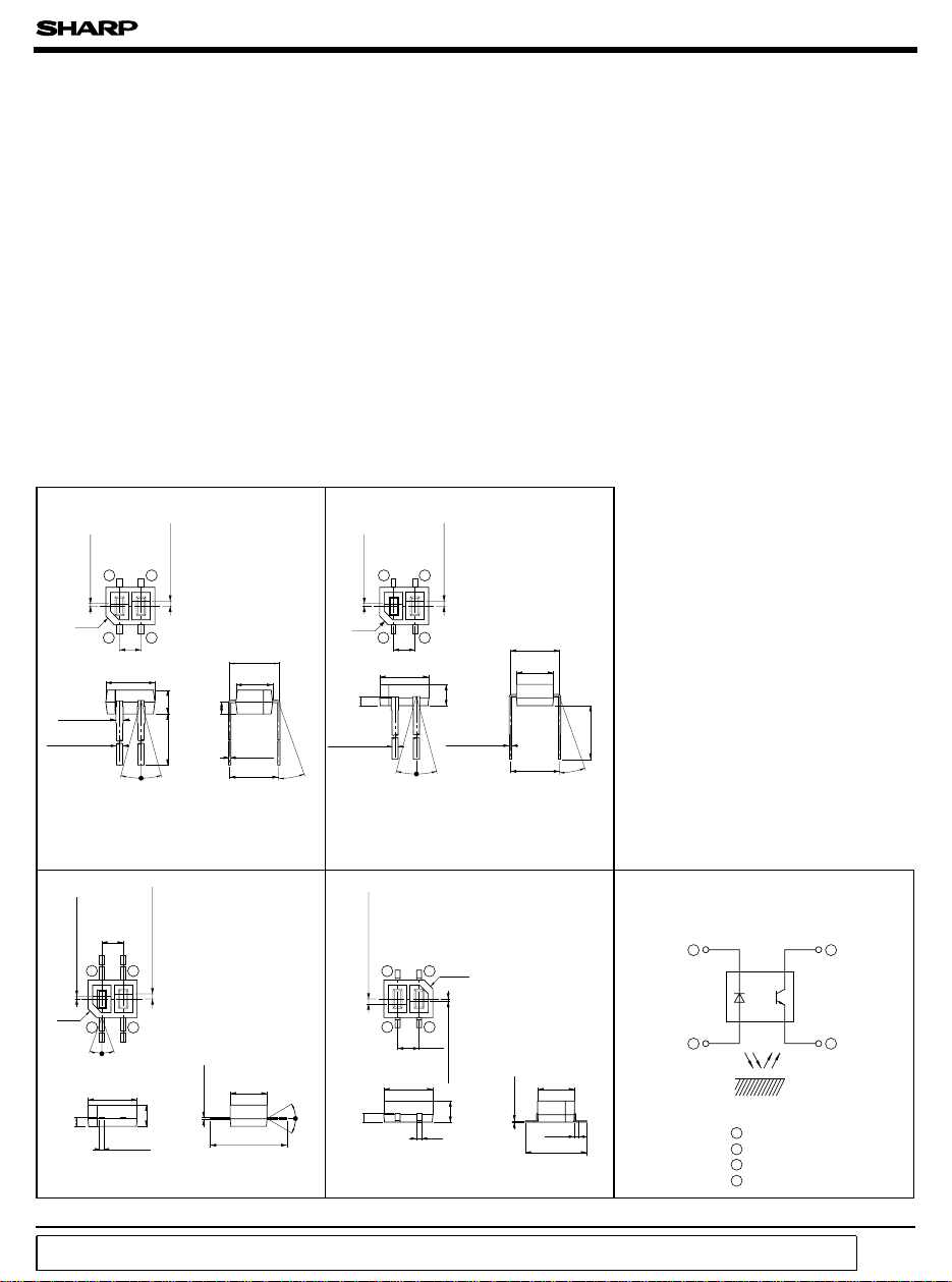
■ Outline Dimensions
GP2S09
+0.2
- 0.1
±15˚
21
+ 0.2
- 0.1
34
2
1.7
Detector center
)
0.4
(
❈4.0
3.0
0.15
±
1.7
0.8
1.0
±
4 - 0.2
12.5
(
Detector center
)
0.4
(
0.2-0.1
3.0
+
0.15
13.0
±0.2
+0.2
- 0.1
+ 0.3
- 0
)
4.0
θ: 0 to 20˚
+0.2
- 0.1
±
1.0
Emitter center
)
0.2
(
C0.7
1
1.75
4.0
)
4-(0.6
+ 0.2
4 -0.5
- 0.1
∗Tolerance:± 0.15mm
∗( ): Reference dimensions
∗The dimensions indicated by ❈ refer
to those measured from the lead base.
GP2S26 GP2S27
1.75
Emitter center
)
43
0.2
(
C0.7
± 20 ˚
0.2
+
0.4
- 0.1
0.75
0.4
∗Tolerance:± 0.15mm
∗( ): Reference dimensions
GP2S24
Emitter center
)
0.2
(
C0.7
0.75
4 - 0.4
θ
∗Tolerance:±0.15mm
∗( ): Reference dimensions
∗The dimensions indicated by ❈ refer
Detector center
)
0.4
(
0.75
± 30˚
43
21
1.75
+ 0.2
4.0
-
0.1
+ 0.2
- 0.1
± 15 ˚
to those measured from the lead base.
12
34
1.75
+
0.2
4.0
-
0.1
0.4
∗Tolerance:±0.15mm
∗( ): Reference dimensions
1. Cassette tape recorders, VCRs
2. Floppy disk drives
3. Various microcomputerized control equip ment
Detector center
)
0.4
(
± 0.2
❈4.0
+ 0.2
3.0
- 0.1
1.7
+ 0.2
4 - 0.15
- 0.1
C0.7
Emitter center
)
0.2
(
1.7
(
4.0
θ : 0 to 20˚
0.2-0.1
+
0.15
3.0
5.0
1.0-0
+
)
3.5
θ
+
0.2
-
0.1
(
)
0.4
MAX.
Subminiature
Photointerrupter
(
Unit : mm
Internal connection diagram
(
Common to 4 models
1
1 Anode
2 Emitter
3 Collector
4 Cathode
)
34
2
)
“ In the absence of confirmation by device specification sheets, SHARP takes no responsibility for any defects that occur in equipment using any of SHARP's devices, shown in catalogs,
data books, etc. Contact SHARP in order to obtain the latest version of the device specification sheets before using any SHARP's device.”
GP2S09/GP2S24/GP2S26/GP2S27
■ Absolute Maximum Ratings
Parameter Rating Unit
Forward current 50 mA
Input
Reverse voltage 6 V
Power dissipation 75 mW
Collector-emitter voltage 35 V
Output
Emitter-collector voltage 6 V
Collector current 20 mA
Collector power dissiipation 75 mW
Total power dissipation 100 mW
Operating temperature - 20 to + 85 ˚C
Storage temperature - 40 to + 100 ˚C
∗1
Soldering temperature 260 ˚C
∗1 Within 5 seconds (Soldering areas for each model are shown below
GP2S09, GP2S24
The hatched area more than
∗2
away from the lower
1mm
edge of package as shown
in the figure below.
∗2
1mm
4mm∗2 GP2S09:
Symbol
I
F
V
R
P
V
CEO
V
ECO
I
C
P
C
P
tot
T
opr
T
stg
T
sol
)
GP2S26
Soldering area:Soldering area:
The hatched area more than
2.0mm away from the both
edges of package as shown
in the figure below.
■ Electro-optical Characteristics
Parameter Symbol Conditions MIN. TYP. MAX. Unit
Input
Forward voltage V
Reverse current I
Output Collector dark current I
∗3
Transfer
characteristics
∗3 The condition and arrangement of the reflective object are shown below.
∗4 Without reflective object
Collector current I
Response time
∗4
Leak current I
Rise time t
Fall time t
F
R
CEO
C
r
f
LEAK
(
Ta = 25˚C
2.0mm2.0mm
)
GP2S27
Soldering area
The hatched area more than
0.5mm away from the both
edges of package as shown
in the figure below.
0.5mm
0.5mm
(
Ta= 25˚C
IF= 20mA - 1.2 1.4 V
VR=6V - - 10 µA
VCE= 20V - 10
-9
-7
10
A
IF= 4mA, VCE= 2V 20 45 120 µ A
VCE= 2V, IC= 100µ A
=1kΩ, d= 1mm
R
L
- 20 100 µs
- 20 100 µs
IF= 4mA, VCE= 2V - - 0.1 µ A
)
The ranking of collector current shall be classified into the following 6 ranks.
(
GP2S09, GP2S24, GP2S26, GP2S27
Rank
∗5
A
B
C
A or B
B or C
A, B or C
Collector-current IC (µ A
20 to 42
34 to 71
58 to 120
20 to 71
34 to 120
20 to 120
)
∗5 GP2S24 and GP2S26 and GP2S27 don't
have A rank.
)
Test Condition and
Arrangement for
Collector Current
Al evaporation
1mm-thick glass

GP2S09/GP2S24/GP2S26/GP2S27
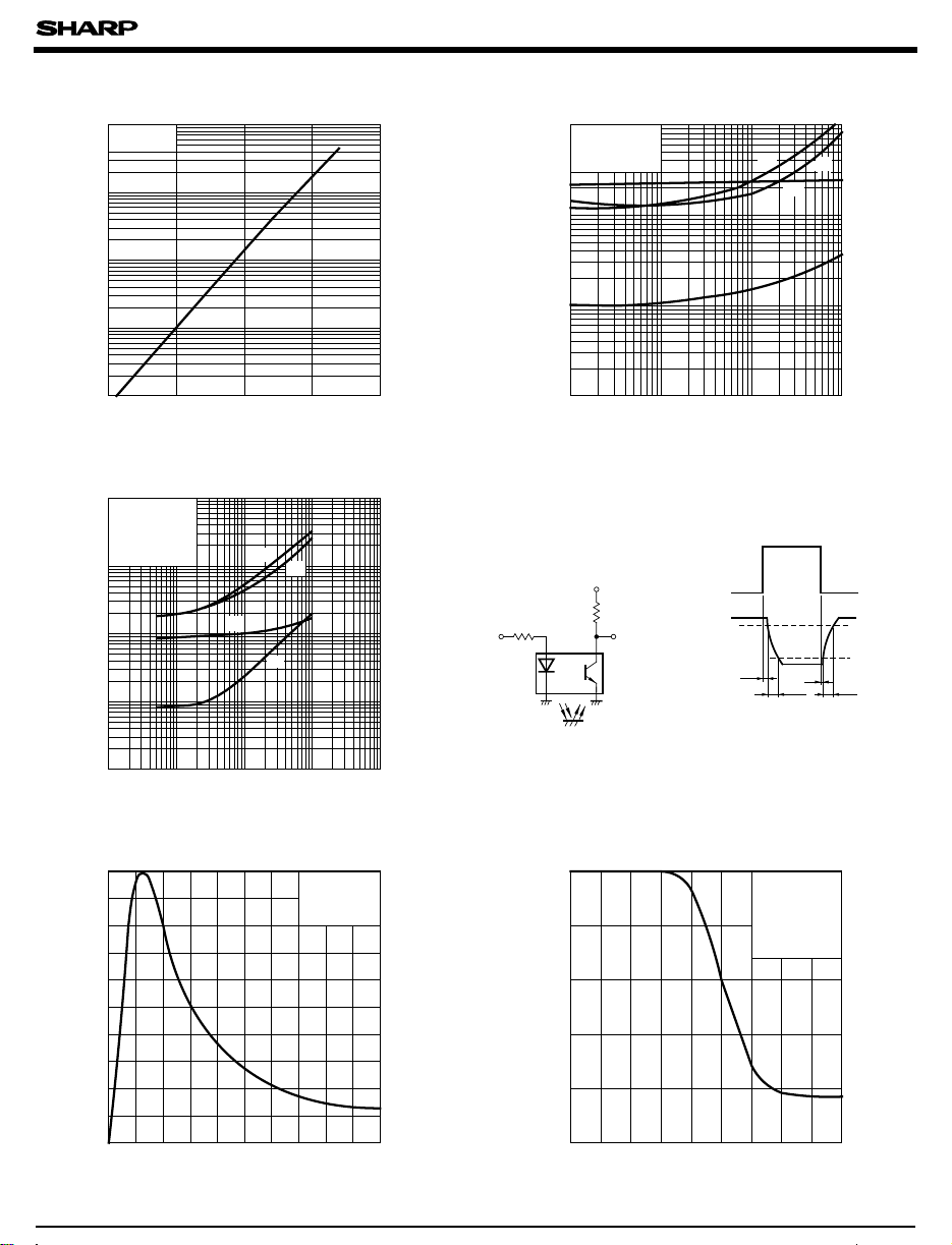
Fig. 1 Forward Current vs.
Ambient Temperature
60
50
)
mA
40
(
F
30
20
Forward current I
10
0
- 25 0 25 50 75 85 100
Ambient temperature Ta (˚C
)
Fig. 3 Forward Current vs.
Forward Voltage Forward Current
500
200
100
)
mA
50
(
F
20
10
5
Forward current I
2
1
Ta= 75˚C
50˚C
25˚C
0
0.5 1 1.5 2 2.5 3
Forward voltage VF (V
)
0˚C
- 25˚C
Fig. 5 Collector Current vs.
Collector-Emitter Voltage
350
Ta=
25˚C
300
)
250
µA
(
C
200
150
100
Collector current I
50
0
2468100
Collector-emitter voltage VCE (V
I
F
10mA
= 15mA
7mA
4mA
2mA
12
)
Fig. 2 Power Dissipation vs.
Ambient Temperature
120
P
tot
100
)
P, P
80
mW
(
60
Power dissipation P
C
40
20
0
025-25
Ambient temperature T
Fig. 4 Collector Current vs.
700
VCE=2V
= 25˚C
T
a
600
)
500
µ A
(
C
400
300
200
Collector current I
100
0
51015 25300
Forward current IF (mA
Fig. 6 Relatlve Collector Current vs.
Ambient Temperature
120
100
)
%
(
C
80
60
40
Relatlve collector current I
20
0
025-25
Ambient temperature T
50 10075
(˚C
a
20
)
50 10075
(˚C
a
85
)
IF= 4mA
V
CE
)
=2V
GP2S09/GP2S24/GP2S26/GP2S27
Fig. 7 Collector Dark Current vs.
Ambient Temperature
-6
10
VCE= 20V
5
2
)
A
-7
(
10
5
CEO
2
-8
10
5
2
-9
10
Collector dark current I
5
2
-10
10
0
5025
75
Ambient temperature Ta (˚C
100
)
Fig. 9 Response Time vs. Load Resistance
(GP2S24/ GP2S26/GP2S27
1000
V
=2V
CE
500
I
= 100 µA
C
200
T
= 25˚C
100
)
50
µ s
(
20
10
5
Response time
2
a
t
r
t
f
t
d
t
s
1
0.5
0.2
0.1
0.1 1 10 100 1000
Load resistance RL (kΩ
)
)
Fig.10 Relative Collector Current vs.
Distance between Sensor and
Al Evaporation Glass
100
80
)
%
(
60
IF= 4mA
V
=2V
CE
T
= 25˚C
a
Fig. 8 Response Time vs. Load Resistance
100
V
=2V
CE
= 100 µA
I
C
50
= 25˚C
T
a
20
)
10
µ s
(
5
2
1
Response time
0.5
0.2
0.1
0.01
0.02
0.2 0.5 1 2 5 10
0.1
0.05
Load resistance RL (kΩ
Test Circuit for Response Time
V
Input
CC
R
R
D
L
Output
Input
Output
t
Fig.11 Relative Collector Current vs.
Card Moving Distance (1
100
80
)
%
(
60
t
r
t
s
d
I
VCE=2V
d= 1mm
T
(
GP2S09
t
d
)
t
s
t
r
)
= 4mA
F
= 25˚C
a
)
t
f
10%
90%
t
f
40
Relative collector current
20
0
012 45
Distance between sensor and Al evaporation glass d (mm
3024
40
Relative collector current
20
0
)
Card moving distance L(mm)
61357

GP2S09/GP2S24/GP2S26/GP2S27
Fig.12 Relative Collector Current vs.
Card Moving Distance (2
100
80
)
%
(
60
40
Relative collector current
20
0
-2 0 2 4
Card moving distance L(mm)
)
IF= 4mA
V
=2V
CE
d= 1mm
= 25˚C
T
a
6-1 1 3 5
Test Condition for Distance & Detecting Position
Characteristics (EX : GP2S24
Correspond to Fig.10
d
Correspond to Fig.11
Test condition
= 4mA
I
F
VCE= 2V
d= 1mm
OMS card
White
L= 0
+
Al evaporated glass
Black Black
Lmm
d
--
Fig.13-a Frequency Response Fig.13-b Frequency Response
=2V
= 100 µA
= 25˚C
1kΩ
)
(GP2S24/ GP2S26/ GP2S27
0
)
dB
(
-5
V
R
= 10kΩ
-10
L
Voltage gain A
-15
0
)
dB
(
-5
V
-10
Voltage gain A
-15
(GP2S09
V
CE
I
C
T
a
= 10kΩ
R
L
)
d
Correspond to Fig.12
Test condition
= 4mA
I
F
V
= 2V
CE
d=1mm
OMS card
White
L= 0
+
)
=2V
V
CE
I
= 100µA
C
T
= 25˚C
a
1kΩ
Lmm
-20
2
2
10
3
5
10
Frequency f (Hz
2
5
Fig.14 Spectral Sensitivity
(Detecting Side
100
80
)
%
(
60
40
Relative sensitivity
20
0
600 700 800 900 1000 1200
)
Wavelength λ (nm
4
2
10
)
T
= 25˚C
a
5
5
10
-20
2
10
●
Please refer to the chapter
3
10
4
10
Frequency f (Hz
10
)
“ Precautions for Use”.
5
6
10
1100
)
 Loading...