

GP2L09/GP2L24/GP2L26
GP2L09/GP2L24
Subminiature, High Sensitivity
Photointerrupter
GP2L26
■ Features ■ Applications
1. Compact and thin
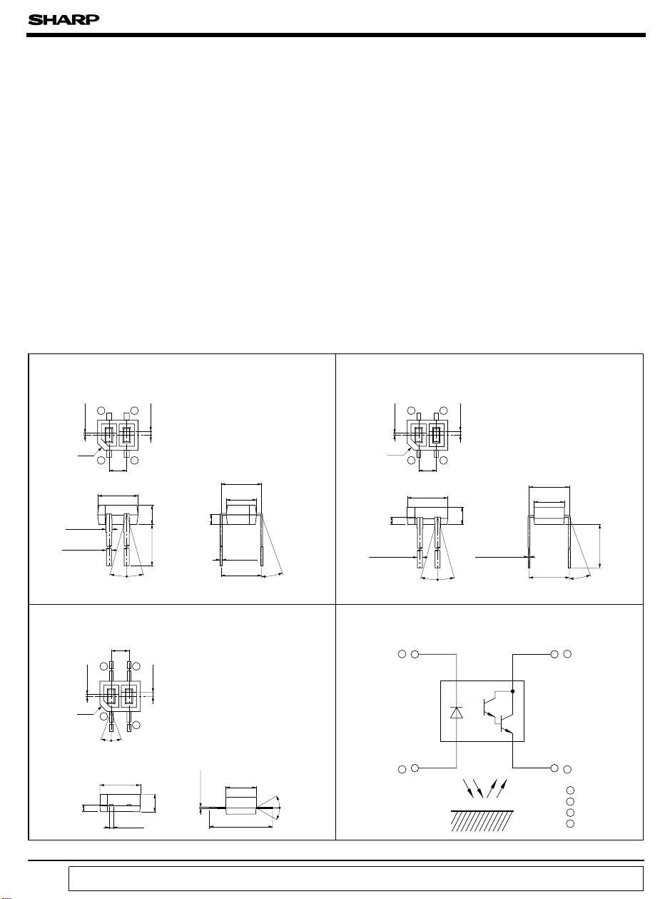
GP2L09: Compact DIP, long lead type
GP2L24: Compact DIP type
GP2L26: Flat lead type
2. Optimum detection distance: 0.6 to 0.8mm
3. High sensitivity
: MIN. 0.5mA at IF= 4mA
(I
C
)
4. Visible light cut-off type
■ Outline Dimensions
GP2L09
+0.2
- 0.1
2
+0.2
- 0.1
Detector center
)
∗
Tolerance:± 0.15mm
0.4
(
( )
∗
: Reference dimensions
∗The dimensions indicated by ❈ refer
to those measured from the lead base.
0.15
0.15
±
1.7
1.0
1.0
±
12.5
Detector center
)
0.4
(
∗Tolerance:± 0.15mm
∗( ): Reference dimensions
2
0.2-0.1
+
0.15
1.7
❈4.0
3.0
0.8
4- 0.2
θ : 0 to 20˚
3.0
13.0
±
0.2
0.2
+ 0.2
- 0.1
+ 0.3
- 0
(
)
4.0
+
0.2
-
0.1
±
1.0
GP2L26
Emitter center
)
0.2
(
C0.7
4-(0.6
+ 0.2
4- 0.5
- 0.1
Emitter center
)
0.2
(
C0.7
0.75
43
1
1.75
+ 0.2
4.0
- 0.1
)
± 15˚
1.75
43
1
± 20˚
4.0
0.4
θ
± 30˚
1. Cassette tape recorders, VCRs
2. Floppy disk drives
3. Various microcomputerized control equip ment
GP2L24
4
Emitter center
)
0.2
(
C0.7
1
1.75
+0.2
4.0
- 0.1
0.75
+0.2
4 - 0.4
- 0.1
±15˚
Internal connection diagram
(
Common to 3 models
4
1
3
2
(
Unit : mm
Detector center
)
∗Tolerance:± 0.15mm
0.4
(
∗( ): Reference dimensions
∗
The dimensions indicated by ❈ refer
to those measured from the lead base.
± 0.2
0.2
❈4.0
+
0.2
3.0
-
0.1
1.7
+ 0.2
4 - 0.15
- 0.1
(
)
4.0
θ
θ:0 to 20˚
)
3
2
1 Anode
2 Emitter
3 Collector
4 Cathode
)
1.0-0
+
3.5
“ In the absence of confirmation by device specification sheets, SHARP takes no responsibility for any defects that occur in equipment using any of SHARP's devices, shown in catalogs,
data books, etc. Contact SHARP in order to obtain the latest version of the device specification sheets before using any SHARP's device.”
GP2L09/GP2L24/GP2L26
■ Absolute Maximum Ratings
Parameter Symbol Rating Unit
Forward current I
Input
Reverse voltage V
Power dissipation
Collector-emitter voltage V
Output
Emitter-collector voltage V
Collector current I
Collector power dissipation
Total power dissipation P
Operating temperature
Storage temperature T
∗1
Soldering temperature
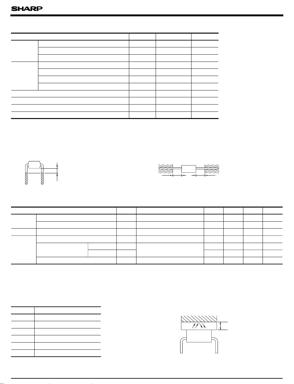
∗1 Within 5 seconds (Soldering areas for each model are shown below.
GP2L09, GP2L24
Soldering area
The hatched area more than 1mm
away from the lower edge of
package as shown in the drawing
below.
∗2
∗2 GP2L09: 4mm
∗2
1mm
F
R
P75
CEO
ECO
C
P
C
tot
T
opr
stg
T
sol
)
- 25 to + 85 ˚C
- 40 to + 100 ˚C
GP2L26
Soldering area
The hatched area more
than 2.0mm away from
the both edge of package
as shown in the drawing
below.
■ Electro-optical Characteristics
Parameter Symbol Conditions MIN. TYP. MAX. Unit
Input
Forward voltage I
Reverse current I
Output Collector dark current I
∗3
Transfercharacteristics
∗3 The condition and arrangement of the reflective object are shown in the right drawing.
∗4 Without reflective object
Collector current I
Response time
∗4
Leak current I
Rise time t
Fall time t
F
R
CEO
C
r
f
LEAK
IF= 20mA - 1.2 1.4 V
VR=6V - - 10 µA
= 10V, I
V
CE
VCE= 2V, IF= 4mA 0.5 3.0 15.0 mA
V
= 2V, IC= 10mA
CE
= 100Ω , d= 1mm
R
L
IF= 4mA, VCE= 5V - - 5.0
(
Ta= 25˚C
)
50 mA
6V
mW
35 V
6V
50 mA
75 mW
100 mW
260 ˚C
=0
2.0mm
- - 1x 10
2.0mm
F
- 80 400
- 70 400
(
Ta= 25˚C
-6
)
A
µ s
µ s
µA
The ranking of collector current shall be
classified into the following 6 ranks.
(
GP2L09, GP2L24, GP2L26
Rank Collector current IC (mA
∗5
A 0.5 to 1.9
B 1.45 to 5.4
C 4.0 to 15.0
A or B 0.5 to 5.4
B or C 1.45 to 15.0
A, B or C
∗5 GP2L24 and GP2L26 don't
have A rank.
0.5 to 15.0
)
)
Test Condition for Collector Current
Al evaporation
1mm-thick glass

GP2L09/GP2L24/GP2L26
Fig. 1 Forward Current vs.
Ambient Temperature
60
50
)
mA
40
(
F
30
20
Forward current I
10
0
- 25 0 25 50 75 85 100
Ambient temperature Ta (˚C
Fig. 3 Peak Forward Current vs.
Duty Ratio
Pulse width <=100 µ s
-2
10
Ta= 25˚C
10
Duty ratio
2000
)
1000
mA
(
FM
500
200
100
Peak forward current I
50
20
-3
2
10
52525
Fig. 5 Collector Current vs.
Forward Current
25
20
)
mA
(
C
15
10
Collector current I
5
0
2.5 5.0 7.5 10.0 12.50
Forward current IF (mA
Fig. 2 Power Dissipation vs.
Ambient Temperature
120
P
tot
100
)
P, P
80
mW
(
Power dissipation P
)
C
75
60
40
20
0
025-25
Ambient temperature T
50 10075
(˚C
a
85
)
Fig. 4 Forward Current vs.
Forward Voltage
500
200
)
100
mA
(
50
F
20
10
Forward current I
5
2
-1
1
1
0
Ta= 75˚C
50˚C
0.5 1.0 1.5 2.0 2.5 3.0
Forward voltage VF (V
25˚C
)
0˚C
-
25˚C
Fig. 6 Collector Current vs.
Collector-emitter Voltage
V
T
)
=2V
CE
= 25˚C
a
15.0
16
14
)
12
10
8
6
4
2
0
IF= 15mA
2468100
mA
(
C
Collector current I
P
(MAX.
c
10mA
7mA
4mA
2mA
Collector-emitter voltage V
CE
T
= 25˚C
a
)
(V
12
)

GP2L09/GP2L24/GP2L26
Fig. 7 Relative Collector Current vs.
Ambient Temperature
150
125
)
%
(
100
75
50
Relative collector current
25
0
025-25
Ambient temperature Ta (˚C
= 4mA
I
F
V
CE
50 10075
)
Fig. 9-a Response Time vs.
Load Resistance
(
Input
Output
GP2L09
t
r
t
f
t
d
t
s
)
t
d
1000
500
200
)
100
µ s
(
50
20
10
Response time
5
2
1
Input R
D
V
=2V
CE
= 10mA
I
C
T
= 25˚C
a
10 20 50 100 200 500 1000 1 10 100 1000 1000
Load resistance RL (Ω
Test Circuit for Response Time
V
CC
R
L
Output
Fig. 8 Collector Dark Current vs.
Ambient Temperature
-4
10
5
=5V
10
)
A
(
10
CEO
10
10
10
Collector dark current I
-10
10
-11
10
-5
5
-6
5
-7
5
-8
5
-9
5
5
-25 0
VCE= 10V
25 10050 75
Ambient temperature Ta (˚C
)
Fig. 9-b Response Time vs.
Load Resistance
)(
)
µ s
(
1000
500
200
100
50
VCE=2V
I
= 10mA
C
= 25˚C
T
a
GP2L24/GP2L26
t
r
t
f
20
10
t
d
5
Response time
2
t
s
1
0.5
0.2
0.1
Load resistance R
)
(Ω
L
)
Fig.10 Relative Collector Current vs.
Distance between Sensor and
Al Evaporation Glass
100
80
)
%
(
60
10%
90%
t
s
t
t
r
f
40
Relative collector current
20
IF= 4mA
=2V
V
CE
= 25˚C
T
a
0
012 45
Distance between sensor and Al evaporation glass
3
d (mm
)

GP2L09/GP2L24/GP2L26
Fig.11 Relative Collector Current vs.
Card Moving Distance(1
100
80
)
%
(
60
40
Relative collector current
20
0
-1 1 3 5
024
Card moving distance L(mm)
)
= 4mA
I
F
V
=2V
CE
d= 1mm
= 25˚C
T
a
6
7 531-1
Test Condition for Distance & Detecting
Position Characteristics
Lmm
)
d
GP2L24
d
Correspond to Fig.12
Test condition
= 4mA
I
F
V
CE
d = 1mm
OMS card
White
+
L=0
/
= 2V
)
(EX.: GP2L24
Correspond to Fig.10
Correspond to Fig.11
Test condition
I
= 4mA
F
VCE= 2V
d = 1mm
d
OMS card
White
+
L= 0
Al evaporation
Black
-
Fig.14 Frequency Response (GP2L24 GP2L26 Fig.15 Spectral Sensitivity (Detecting Side
Fig.12 Relative Collector Current vs.
Card Moving Distance(2
100
)
80
%
(
60
40
Relative collector current
20
0
Card moving distance L(mm)
Fig.13 Frequency Response
0
)
dB
(
-5
3
5
10
RL=1kΩ
2
Frequency f (Hz
Black
Lmm
-
-10
Voltage gain Av
-15
-20
2
2
10
)
IF= 4mA
V
=2V
CE
d= 1mm
= 25˚C
T
a
420-2
VCE=2V
I
=10mA
C
T
= 25˚C
a
5
10
10Ω
5
)
2
(
GP2L09
100Ω
4
2
5
10
)
6
)
5
0
)
dB
(
-5
-10
Voltage gain Av
-15
-20
2
10
=1kΩ
R
L
3
10
Frequency f (kHz
IF= 10mA
V
=2V
CE
T
= 25˚C
a
100Ω
4
10
10Ω
5
10
)
6
10
100
80
)
%
(
60
40
Relative sensitivity
20
0
600 700 800 900 1000 1200
Wavelength λ (nm
Ta= 25˚C
)
1100

GP2L09/GP2L24/GP2L26
■ Precautions for Use
(1)
In order to stabilize power supply line, connect a by-pass capacitor of more than 0.01µF bet-
ween Vcc and GND near the device.
(2)
In this product, the PWB is fixed with a resin cover, and cleaning solvent may remain inside
the case; therefore, dip cleaning or ultrasonic cleaning are prohibited.
(3)
Remove dust or stains, using an air blower or a soft cloth moistened in cleaning solvent.
However, do not perform the above cleaning using a soft cloth with cleaning solvent in the
marking portion.
In this case, use only the following type of cleaning solvent used for wiping off:
Ethyl alcohol, Methyl alcohol, Isopropyl alcohol, Freon TE, Freon TF, Diflon solvent S3-E
When the cleaning solvents except for specified materials are used, please consult us.
(4)
As for other general cautions, refer to the chapter “ Precautions for Use ”.
 Loading...