

Page 1
GP2L01/GP2L01F
GP2L01/GP2L01F
High Sensitivity, Long Focal
Distance Type
Photointerrupter
■ Features
1. Long focal distance
2. High current transfer ratio
GP2L01 CTR: MIN. 30%
GP2L01F CTR: MIN. 25%
}
at I
2. Visible light cut-off type: GP2L01F
■ Applications
1. Copiers, printers
2. Automatic vending machines, ticket vend ing machines
3. Optoelectronic switches, optoelectronic
counters
= 10mA
F
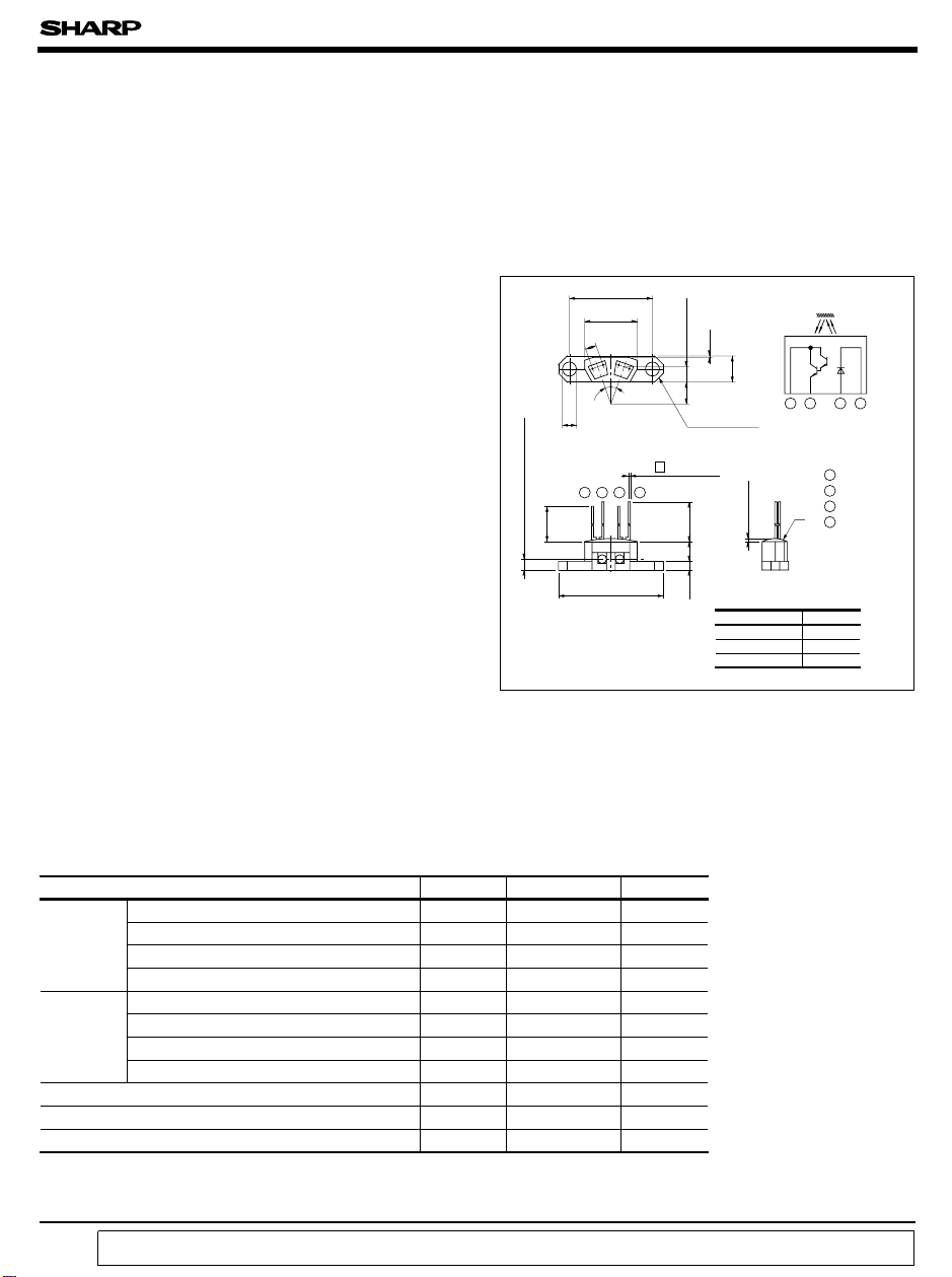
■ Outline Dimensions
±
0.2
19.0
12.0
)
2 -(2.54
2 - 19.5 ˚
±
0.2
2- φ 3.2
4- 0.45
1.0
Detector center
±
)
2.5
16.0
(
1234
24.0
(
Unit : mm
)
3.5
(
2 -
)
5.0
(
4 - C2.0
±
0.2
1.0
±
17.0
4.52.0
Internal connection
diagram
0.3
6.0
1 Cathode
MAX.
0.7
❈ Protrusion of resin for fixing
∗Unspecified tolerances shall be as follows;
Dimensions(d
d<= 6.0 ± 0.1
6.0<d<= 18.0 ± 0.2
18.0<d<= 24.0 ± 0.25
∗( ): Reference dimensions
2 Anode
3 Emitter
❈
4 Collector
)
Tolerance
)
1234
■ Absolute Maximum Ratings
(
Ta = 25˚C
)
Parameter Symbol Rating Unit
Input
Forward current I
∗1
Peak forward current I
Reverse voltage V
F
FM
R
50 mA
1A
6V
Power dissipation P 75 mW
Collector-emitter voltage V
Output
Emitter-collector voltage V
Collector current I
Collector power dissipation P
Operating temperature
Storage temperature T
∗2
Soldering temperature T
∗1 Pulse width<=100 µs, Duty ratio= 0.01
∗2 For 3 seconds
“ In the absence of confirmation by device specification sheets, SHARP takes no responsibility for any defects that occur in equipment using any of SHARP's devices, shown in catalogs,
data books, etc. Contact SHARP in order to obtain the latest version of the device specification sheets before using any SHARP's device.”
CEO
ECO
C
C
T
opr
stg
sol
35 V
6V
40 mA
75 mW
- 25 to + 85 ˚C
- 40 to + 100 ˚C
260 ˚C
Page 2
GP2L01/GP2L01F
■ Electro-optical Characteristics
Parameter Symbol Conditions MIN. TYP. MAX. Unit
Forward voltage V
Input
Peak forward voltage V
Reverse current I
Output Collector dark current I
∗3
Collector
Transfer
characteristics
Current
Response time
∗4
Leak current I
∗3 Test method : A reflective object shall be an OMS test card (white) specified by Sharp, and be 5.0mm away from the sensor.
∗
4 Wihtout reflective object
GP2L01
GP2L01F 2.5 - 25
Rise time
Fall time t
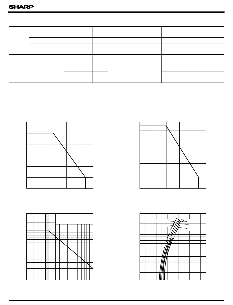
Fig. 1 Forward Current vs.
Ambient Temperature
60
50
)
mA
40
(
F
30
20
Forward current I
10
0
- 25 0 25 50 75 85 100
Ambient temperature Ta (˚C
)
Fig. 3 Peak Forward Current vs. Duty Ratio
IF= 20mA - 1.2 1.4 V
F
FMIFM
R
CEO
Ic I
t
r
f
LEAK
= 0.5A - 3.0 4.0 V
VR=3V - - 10
VCE= 10V - - 10
= 10mA, VCE=2V
F
IC= 10mA, VCE= 2V, RL= 100Ω
d= 5mm
IF= 10mA, VCE=2V
3--
- 80 400
- 70 350
- - 100
Fig. 2 Collector Power Dissipation vs.
Ambient Temperature
80
75
70
)
mW
60
(
C
50
40
30
20
Collector power dissipation P
10
0
- 25 0 25 50 75 85 100
Ambient temperature Ta (˚C
Fig. 4 Forward Current vs. Forward Voltage
)
(
Ta= 25˚C
-6
)
µA
A
mA
mA
µs
µs
µA
2000
)
1000
mA
(
500
FM
200
100
Peak forward current I
50
20
- 3
2
10
Pulse width <=100 m s
Ta= 25˚C
- 2
52525
10
Duty ratio
- 1
10
1
500
200
)
100
mA
(
50
F
20
10
5
Forward current I
2
1
0
0.5 1.0 1.5 2.0 2.5 3.0
Ta= 75˚C
50˚C
Forward voltage VF (V
25˚C
0˚C
)
- 25˚C
Page 3

GP2L01/GP2L01F
Fig. 5 Collector Current vs. Forward Current Fig. 6 Collector Current vs.
Collector-emitter Voltage
25
VCE=2V
T
= 25˚C
a
20
)
mA
(
C
15
10
Collector current I
5
0
5101520250
Forward current IF (mA
)
Fig. 7 Relative Collector Current vs.
Ambient Temperature
125
= 10mA
I
F
V
=2V
CE
100
)
%
(
75
50
Relative collector current
25
0
025-25
50 10075
Ambient temperature Ta (˚C
30
)
30
)
mA
(
25
IF= 20mA
20
C
15mA
P
(MAX.
C
15
10mA
10
Collector current I
5
0
12 34 50
Collector-emitter voltage V
Fig. 8 Collector Dark Current vs.
Ambient Temperature
-4
10
5
VCE= 10V
-5
10
5
)
A
(
-6
10
5
CEO
-7
10
5
-8
10
5
-9
10
5
Collector dark current I
-10
10
5
-11
10
- 25 0 25 10050 75
Ambient temperature Ta (˚C
Ta= 25˚C
)
5mA
610987
)
(V
CE
)
Fig. 9 Response Time vs. Load Resistance
1000
500
200
)
100
µ s
(
50
20
10
Response time
=2V
V
CE
I
= 10mA
C
T
= 25˚C
a
5
2
1
10 20 50 100 200 500 1000
5
Load resistance R
(Ω
L
t
r
t
f
t
d
t
s
)
Input R
Test Circuit for Response Time
V
CC
R
D
L
Output
Output
Input
t
d
10%
90%
t
s
t
t
r
f
Page 4

GP2L01/GP2L01F
Fig.10 Frequency Response
V
0
)
dB
(
-5
V
-10
Voltage gain A
-15
-20
2
25 2 255
10
=1kΩ
R
L
3
10
Frequency f (Hz
100Ω
4
10
CE
I
= 10mA
C
T
= 25˚C
a
10Ω
5
10
)
Fig.12 Relative Collector Current vs.
Card Moving Distance
100
IF= 10mA
V
)
80
%
(
60
40
Relative collector current
20
CE
d= 5mm
T
a
=2V
2
=2V
= 25˚C
Fig.11 Relative Collector Current vs.
Distance between GP2L01(F) and Test Card
100
80
)
%
(
60
40
Relative collector current
20
5
0
0246810
13 5 79
Distance between
GP2L01(F
I
= 10mA
F
=2V
V
CE
= 25˚C
T
a
)
and test card d (mm
)
Distance Characteristic Test Conditions
Correspond to Fig.11
SHARP OMS TEST CARD
(
)
White
Correspond to Fig.12
SHARP OMS TEST CARD
Black White
d
-+
0
GP2L01
(
GP2L01F
)
d
0
-10 -8 -6 -4 -2 0
Card moving distance L(mm)
2
4
Fig.13 Collector Current vs. Illuminance (Reference
100
50
20
)
10
mA
(
C
5
2
1
Collector current I
0.5
0.2
0.1
100 200 1000 2000 5000
Illuminance under fluorescent lamp (1x
PT431
PT431F
500
Test condition
Light source: White fluorescent lamp
Sharp FLR-40SW/M
= 2V, Ta= 25˚C
V
CE
(
Note) Comparison between outputs of
transparent resin molded type photo transistor (PT431) and visible light
cut-off type (PT431F
)
)
)
●
Please refer to the chapter
Card moving direction
(
GP2L01
(
GP2L01F
Distance= L
)
“Precautions for Use” .
)
 Loading...