

Page 1
GP1A15
GP1A15
High Sensing Accuracy Type OPIC
Photointerrupter
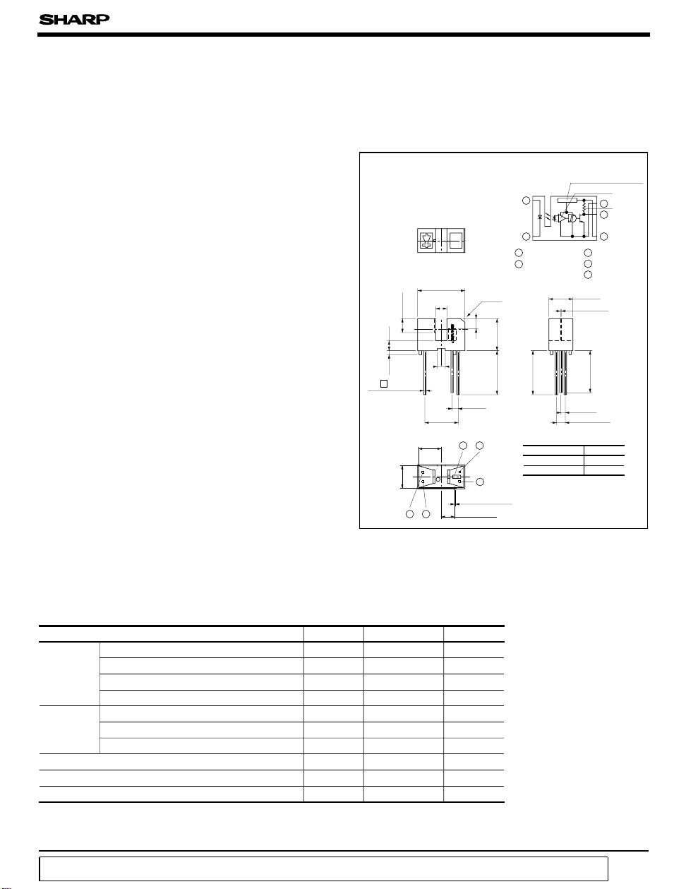
■ Features ■ Outline Dimensions
1. High sensing accuracy
(slit width : 0.25mm
2. Built-in schmidt trigger circuit
3. Low threshold input current
(I
: MAX. 10mA
FLH
4. Low level supply current
(I
: MAX. 5mA
CCL
5. Operating supply voltage V
6. TTL and CMOS compatible output
■ Applications
1. Floppy disk drives
2. Copiers, printers, facsimiles
3. Opetoelectronic switches, optoelectronic
counters
)
)
0.25
)
: 4.5 to 17V
CC
2.5
2 - 0.7
5-0.45
*“ OPIC” (Optical IC) is a trademark of the SHARP Corporation.
An OPIC consists of a light-detecting element and signal processing circuit integrated onto a single chip.
+ 0.1
±
-
3.7
0.2
5.26
12.0
0
+ 0.2
-
0.1
)
1A15
(
1.5
43
2 - φ 0.7
±
3.5
C0.5
)
5
0.1
0.15
+0-
2.0
+ 0.3
-
3.0
2.3
0.1
(
8.8
±
0.1
5.5
12
(
Unit : mm
Internal connection
diagram
1
23
1 Anode
2 Cathode
8.0
MIN.
MIN.
12.0
-
11.0
3
*Unspecified tolerances shall be as follows;
Dimensions(d
6.0< d<=12.0 ± 0.25
*( ): Reference dimensions
±
0.1
Voltage regulator
5
4
3 V
CC
4 V
O
5 GND
6.0
±
0.05
0.25
Slit width
(
Both sides of
emitter and
detector
MIN.
10.5
(
)
1.27
)
2 -(2.54
)
Tolerance
d<=6.0 ± 0.15
)
Amp.
(
10kΩ
)
)
■ Absolute Maximum Ratings
(
Ta= 25˚C
)
Parameter Symbol Rating Unit
Input
Forward current I
*1
Peak forward current I
Reverse voltage V
F
FM
R
50 mA
1A
6V
Power dissipation P 75 mW
Supply voltage V
Output
Output current I
Power dissipation P
Operating tamperature T
Storage temperture T
*2
Soldering temperature T
*1 Pules width
*2 For 5 seconds
“ In the absence of confirmation by device specification sheets, SHARP takes no responsibility for any defects that occur in equipment using any of SHARP's devices, shown in catalogs,
data books, etc. Contact SHARP in order to obtain the latest version of the device specification sheets before using any SHARP's device.”
<=100µs, Duty ratio = 0.01
opr
stg
sol
- 0.5 to + 17 V
CC
O
O
- 25 to + 85 ˚C
- 40 to + 100 ˚C
50 mA
250 mW
260 ˚C
Page 2
GP1A15
■ Electro-optical Charcateristics
Parameter Conditions MIN. TYP. MAX. Unit
Input
Forward voltage I
Reverse current V
Operating supply voltage 4.5 - 17 V
Low level output voltage V
Output
High level output voltage V
Low level supply current I
High level supply current I
*3
“ Low→High” threshold input current
*4
Transfer
charac-
teristics
*3 I
represents forward current when output goes from low to high.
FLH
represents forward current when output goes from high to low.
*4 I
FHL
Hysteresis stands for I
Hysteresis
“ Low→High” propagation delay time
“ High→Low” propagation delay time
Rise time t
Response time
Fall time t
.
FHL/IFLH
Symbol
V
V
I
I
FHL/IFLH
t
t
■ Recommended Operating Conditions
Parameter Symbol
Low level output current
Forward current I
I
OL
Operating temperature
Ta= 0 to + 70˚C
F
= 10mA - 1.15 1.4 V
F
F
I
CCLVCC
CCHVCC
FLH
PLH
PHL
=3V - - 10 µA
R
R
CC
= 16mA, VCC= 5V, IF= 0 - 0.15 0.4 V
OLIOL
OHVCC
= 5V, IF= 10mA 4.9 - - V
= 5V, IF= 0 - 2.5 5.0 mA
= 5V, IF= 10mA - 1.0 3.0 mA
VCC=5V
0.2 2.5 10 mA
0.55 0.75 0.95 -
-
r
f
VCC=5V
I
=10mA
F
R
=280Ω
L
-
- 0.1 0.5
- 0.05 0.5
MIN. MAX. Unit
- 16.0 mA
12.5 20.0 mA
(
Ta= 25˚C
39
515
)
µs
Fig. 1 Forward Current vs. Ambient
Temperature
50
)
mA
40
(
F
30
20
Forward current I
10
0
0
Ambient temperature Ta (˚C
)
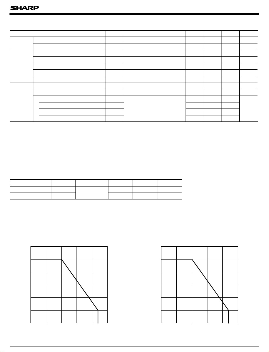
Fig. 2 Output Power Dissipation vs.
Ambient Temperature
300
)
250
mW
(
O
200
150
100
50
Output power dissipation P
0
100755025
85- 25
- 25
0
25 50 75 100
Ambient temperature Ta (˚C
85
)
Page 3

GP1A15
Fig. 3 Low Level Output Current vs.
Ambient Temperature
60
)
50
mA
(
OL
40
30
20
Low level output current I
10
0
- 25 85
0
25 50 75 100
Ambient temperature Ta (˚C
)
Fig. 5 Relative Threshold Input Current vs.
Supply Voltage
1.2
= 25˚C
T
a
I
FLH
I
FHL
/I
I
FLH
FHL
1.0
0.8
0.6
0.4
Fig.4 Forward Current vs. Forward Voltage
500
Ta= 75˚C
50˚C 25˚C
-
0˚C
25˚C
)
mA
(
200
100
50
F
20
10
Forward current I
5
2
1
0 0.5 1.0 1.5 2.0 2.5 3.0
Forward voltage VF (V
)
Fig. 6 Relative Threshold Input Current vs.
Ambient Temperature
1.4
VCC=5V
1.2
I
FLH
1.0
I
0.8
FHL
/I
I
FLH
FHL
I
= 1 at VCC=5V
0.2
FLH
Relative threshold input current
0
0
5
Supply voltage V
)
(V
CC
Fig. 7 Low Level Output Voltage vs.
Low Level Output Current
1.0
0.5
)
V
(
OL
0.2
0.1
0.05
Low level output voltage V
0.02
0.01
Low level output current I
V
T
(mA
OL
=5V
CE
= 25˚C
a
502052
)
0.6
Relative threshold input current
0.4
201510
-25
I
= 1 at Ta= 25˚C
FLH
0
Ambient temperature T
a
(˚C
100755025
)
Fig. 8 Low Level Output Voltage vs.
Ambient Temperature
0.4
)
V
(
0.3
OL
0.2
0.1
Low level output voltage V
100101
0
-25
0
25 50 75 100
Ambient temperature T
V
IOL= 30mA
)
(˚C
a
CC
16mA
=5V
5mA
Page 4

GP1A15
Fig. 9 Supply Current vs. Supply Voltage
6
5
)
mA
(
4
CCL
3
I
CCL
2
Supply current I /ICCH
1
I
CCH
Ta=- 25˚C
25˚C
85˚C
T
=- 25˚C
a
25˚C
85˚C
0
414
268101216
Supply voltage V
)
(V
CC
Fig.11 Rise Time, Fall Time vs.
Load Resistance
0.5
0.4
)
µ s
(
f
,t
r
0.3
0.2
= 10mA
I
F
V
=5V
CC
T
= 25˚C
a
t
r
Fig.10 Propagation Delay Time vs.
Forward Current
7
)
6
µs
(
5
PHL
,t
PLH
4
3
2
1
Propagation delay time t
0
0
10
Forward current IF (mA
20 30
VCC=5V
R
T
)
t
PHL
t
PLH
= 280Ω
L
= 25˚C
a
40 50
Rise time, fall time t
0.1
0
Load resistanc R
t
L
f
(kΩ
520.5
1010.2
)
Test Circuit for Response Time
47Ω
Voltage regulator
Amp.
10kΩ
+ 5V
280Ω
Output
0.01mF
Input
Output
50%
t
PLH
t
PHL
10%
t
r
Input
= tf= 0.01ms
t
r
Z
= 50Ω
O
= 10mA
I
F
■ Precautions for Use
(1) In order to stabilize power supply line, connect a by-pass capacitor of more than 0.01µ F
between Vcc and GND near the device.
(2) As for other general cautions, refer to the chapter “Precautions for Use”.
t
90%
f
V
1.5V
V
OH
OL
 Loading...