GL533
GL533
High Speed Infrared Emitting
Diode for Camera AF
(Automatic Focusing)
■
Features
1. Small spot light diameter for easy beam diaphragming
(TYP. : φ0.6 mm)
2. H
igh positional accuracy of optical axis (accuracy : ± 0.1 mm)
3. High output type (radiant flux Φe : TYP. 13mW)
4. Low peak forward voltage type
(peak forward voltage V
5.
PSD* Equivalent to peak sensitivity wavelength of detectors
: TYP. 2.0V
FM
)
(PD3101F and PD3151F)
(peak emission wavelength : TYP. 940 nm)
PSD* : Position Sensitive Device
■
Applications
1. Cameras
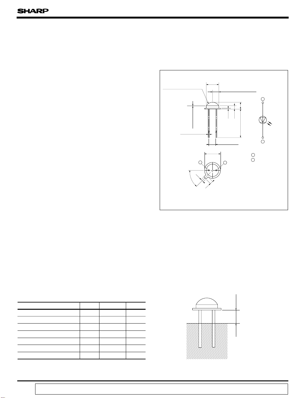
Outline Dimensions
■
Transparent epoxy resin
(Refractive index 1.54)
0.07
Chip top face
position
± 0.1
2 - φ 0.45
1
1.0
45˚
❈ Dimension at lead root
* ( ) : Reference dimensions
4.2
1.0
± 0.1
φ 5.4
Chip position 2.1
0.3
± 0.3
(❈)
2.5
2
1.1
)
2.3
(
)
13.5
(
(Unit : mm)
± 0.1
1
2
1 Anode
2 Cathode
Absolute Maximum Ratings
■
Parameter Symbol Rating Unit
Forward current
*1
Peak forward current
Reverse voltage
Power dissipation
Operating temperature
Storage temperature
*2
Soldering temperature
*1 Pulse width <=100 µ s, Duty ratio=0.01
*2 For MAX. 3 seconds at the position of 1.3 mm from the bottom surface of resin
“ In the absence of confirmation by device specification sheets, SHARP takes no responsibility for any defects that occur in equipment using any of SHARP's devices, shown in catalogs,
data books, etc. Contact SHARP in order to obtain the latest version of the device specification sheets before using any SHARP's device.”
I
F
I
FM
V
R
P 120 mW
T
- 25 to +100
opr
T
- 30 to +100
stg
T
sol
(Ta=25˚C)
80
1
mA
A
6V
˚C
˚C
260 ˚C
1.3mm
Soldering area

GL533
Electro-optical Characteristics
■
Parameter Symbol Conditions MIN. TYP. MAX. Unit
Forward voltage
Peak forward voltage
Reverse current
Radiant flux
Peak emission wavelength
Half intensity wavelength
Terminal capacitance
Response capacitance
(Ta=25 ˚C)
V
F
V
FM
I
R
Φ e
λpI
∆λ I
Ct V
IF= 50mA - 1.3 1.6 V
IFM= 0.5A - 2.0 2.9 V
VR=3V - - 10 µA
= 50mA 8 13 18 mW
I
F
= 20mA - 940 - nm
F
= 20mA - 60 - nm
F
= 0, f= 1MHz - 70 - pF
R
fc - 300 - kHz
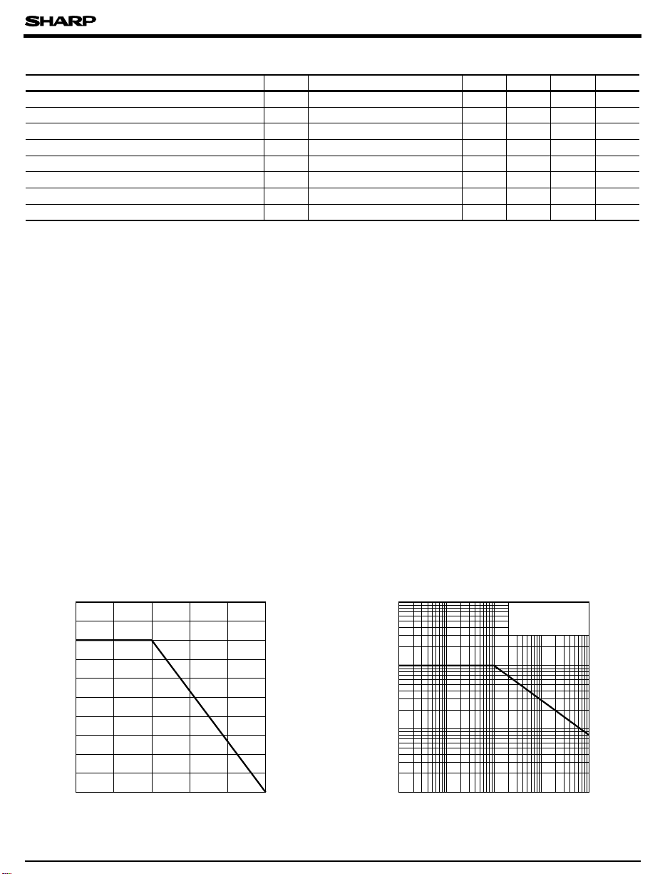
Fig. 1 Forward Current vs. Ambient
Temperature
100
)
mA
(
F
50
Forward current I
0
- 25 0 25 50 75 100
Ambient temperature Ta (˚C
●
Please refer to the chapter "Precautions for Use". (Page 78 to 93)
)
Fig. 2 Peak Forward Current vs. Duty Ratio
-2
10
Duty ratio
Pulse width<=100 µs
Ta= 25˚C
-1
10
10˚
5000
)
mA
(
1000
FM
500
100
50
Peak forward current I
10
-4
10
10
-3
 Loading...