

SERVICE MANUAL
OPERATE
OPEN/CLOSE PLAY STOP SKIP
REW FWD
SERVICE MANUAL
S43Y9DV-SL10H
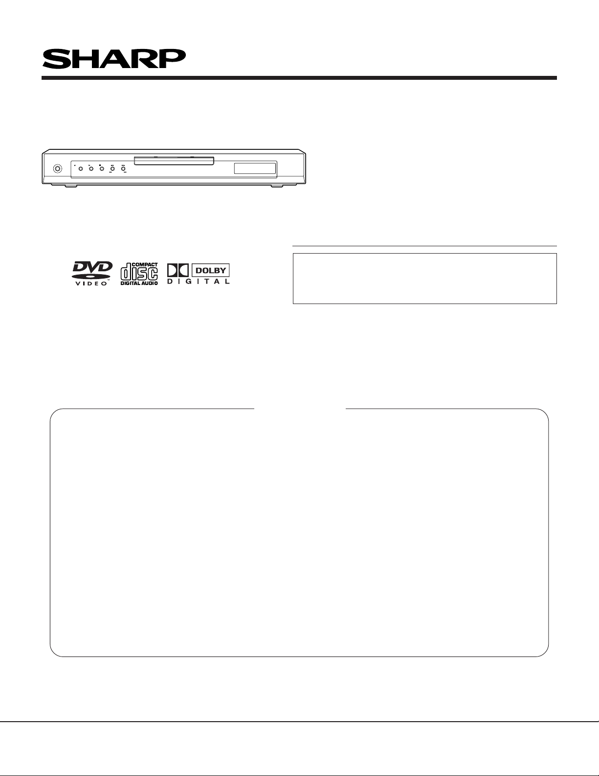
DVD VIDEO PLAYER
DV-SL10H
DV-SL10S(Y)
DVD VIDEO PLAYER
SPECIFICATIONS ............................................................................................................................. 1-1-1
LASER BEAM SAFETY PRECAUTIONS .......................................................................................... 1-2-1
IMPORTANT SAFEGUARDS AND PRECAUTIONS......................................................................... 1-3-1
STANDARD NOTES FOR SERVICING............................................................................................. 1-4-1
MODELS DV-SL10H/DV-SL10S(Y)/DV-SL10S(R)
OPERATING CONTROLS AND FUNCTIONS .................................................................................. 1-5-1
CABINET DISASSEMBLY INSTRUCTIONS ..................................................................................... 1-6-1
TEST MODE ...................................................................................................................................... 1-7-1
TROUBLESHOOTING .......................................................................................................................1-8-1
BLOCK DIAGRAMS........................................................................................................................... 1-9-1
SCHEMATIC DIAGRAMS/ CBA’S AND TEST POINTS ..................................................................1-10-1
WAVEFORMS.................................................................................................................................. 1-11-1
WIRING DIAGRAM ..........................................................................................................................1-12-1
SYSTEM CONTROL TIMING CHARTS .......................................................................................... 1-13-1
IC PIN FUNCTION DESCRIPTIONS ...............................................................................................1-14-1
LEAD IDENTIFICATIONS................................................................................................................ 1-15-1
EXPLODED VIEWS .........................................................................................................................1-16-1
MECHANICAL PARTS LIST ............................................................................................................1-17-1
ELECTRICAL PARTS LIST ............................................................................................................. 1-18-1
MODELS
In the interests of user-safety (Required by safety regulations in some countries) the set should be restored to its
original condition and only parts identical to those specified
be used.
CONTENTS
DV-SL10S(R)
Page
SHARP CORPORATION
This document has been published to be used for
after sales service only.
The contents are subject to change without notice.
1
[ DV -SL10H ]
SPECIFICATIONS
[ DV-SL10S(Y)/DV-SL10S(R) ]
1-1-1
E5752SP
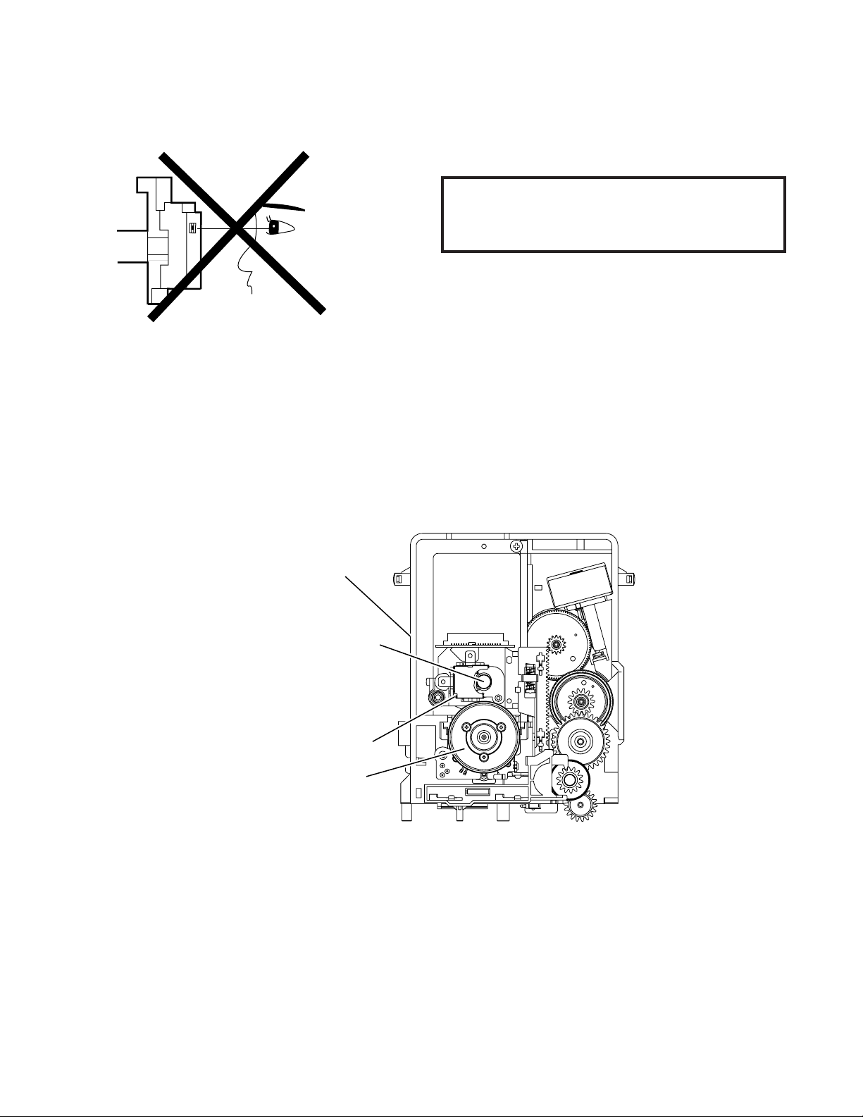
LASER BEAM SAFETY PRECAUTIONS
D
This DVD player uses a pickup that emits a laser beam.
Do not look directly at the laser beam coming
from the pickup or allow it to strike against
your skin.
The laser beam is emitted from the location shown in the figure. When checking the laser diode, be sure to keep your
eyes at least 30cm away from the pickup lens when the diode is turned on. Do not look directly at the laser beam.
Caution: Use of controls and adjustments, or doing procedures other than those specified herein, may result in
hazardous radiation exposure.
rive Mecha Assembly
Laser Beam Radiation
Laser Pickup
Turntable
1-2-1
DVD_LASER
IMPORTANT SAFEGUARDS AND PRECAUTIONS
T
M
T
M
1. IMPORTANT SERVICE NOTES
BEFORE RETURNING THE DVD VIDEO PLAYER
Before returning the DVD video player to the user,
perform the following safety checks.
1. Inspect all lead dress to make certain that leads are
not pinched or that hardware is not lodged between
the chassis and other metal parts in the DVD video
player.
2. Inspect all protective devices such as non-metallic
control knobs, insulation materials, cabinet backs,
adjustment and compartment covers or shields, isolation resistor/capacitor networks, mechanical insulators etc.
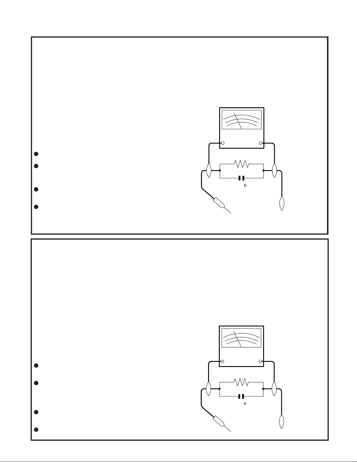
3. To be sure that no shock hazard exists, check for
current in the following manner.
Plug the AC line cord directly into a 230 volt AC outlet
(Do not use an isolation transformer for this test).
Using two clip leads, connect a 1.5k ohm, 10 watt
resistor paralleled by a 0.15µF capacitor in series with
all exposed metal cabinet parts and a known earth
ground, such as a water pipe or conduit.
Use an DVM or VOM with 1000 ohm per volt, or higher,
sensitivity or measure the AC voltage drop across the
resistor (See Diagram).
Move the resistor connection to earth exposed metal
part having a return path to the chassis (metal cabinet,
screw heads, knobs and control shafts, etc.) and
measure the AC voltage drop across the resistor.
Reverse the AC plug on the set and repeat AC voltage
measurements for each exposed part. Any reading of
1.4V rms (this corresponds to 0.7mA rms AC.) or more
is excessive and indicates a potential shock hazard
which must be corrected before returning the DVD
video player to the owner.
SSVM
AC SCALE
2k ohms.
10W
F
0.15
TEST PROBE
O EXPOSED
ETAL PARTS
CONNECT TO
KNOWN EARTH
GROUNG
1. NOTES DE SERVICE IMPORTANTES
AVANT DE RENDRE LE REPRODUCTOR DE VíDEO
DVD
Avant de rendre le reproductor de vídeo DVD à l’utilisateur,
effectuer les vérifications de sécurité suivantes.
1. Vérifier toutes les gaines de fil pour être sûr que les fils
ne sont pas pincés ou que le matériel n’est pas coincé
entre le châssis et les autres pièces métalliques dans le
reproductor de vídeo DVD.
2. Vérifier tous les dispositifs de protection tels que les
boutons de commande non métalliques, les matériaux
d’isolement, le dos du coffret, les couvercles de
compartiment et ajustement ou les boucliers, les
réseaux de résistance / condensateur d’isolement, Ies
isolateurs mécaniques, etc.
3. Pour être sûr qu’il n’y a aucun risque de choc électrique,
vérifier le courant de fuite de la maniére suivante.
Brancher le cordon d’alimentation secteur directement
dans une prise de courant de 230 volts. (Ne pas utiliser
de transformateur d’isolement pour cet essai).
Utiliser deux fils à pinces et connecter une résistance
de 10 watts 1,5 kohm en parallèle avec un condensateur
de 0,15 µF en série avec des pièces du coffret métallique
exposées et une masse de terre connue telle qu’un
tuyau ou un conduit d’eau.
Utiliser un DVM ou VOM avec une sensibilité de 1000
ohms par volt ou plus ou mesurer la chute de tension
CA entre la résistance (voir diagramme).
Déposer la connexion de la résistance à toutes les
pièces métalliques exposées ayant un parcours de
retour au châssis (coffret métallique, tétes de vis, boutons et arbres de commande, etc.) et mesurer la chute
de tension CA entre la résistance. Inverser la fiche CA
(une fiche intermédiaire non polarisée doit être utilisée
à seule fin de faire ces vérifications.) sur l’appareil et
répéter les mesures de tension CA pour chaque piéce
métallique exposée. Toute lecture de 1,4 V rms (ceci
correspond à 0,7 mA rms CA) ou plus est excessive et
signale un danger de choc qui doit être corrigé avant de
rendre le reproductor de vídeo DVD à son utilisateur.
SSVM
AC SCALE
2k ohms.
10W
F
0.15
TEST PROBE
O EXPOSED
ETAL PARTS
CONNECT TO
KNOWN EARTH
GROUNG
1-3-1
E5752IMP
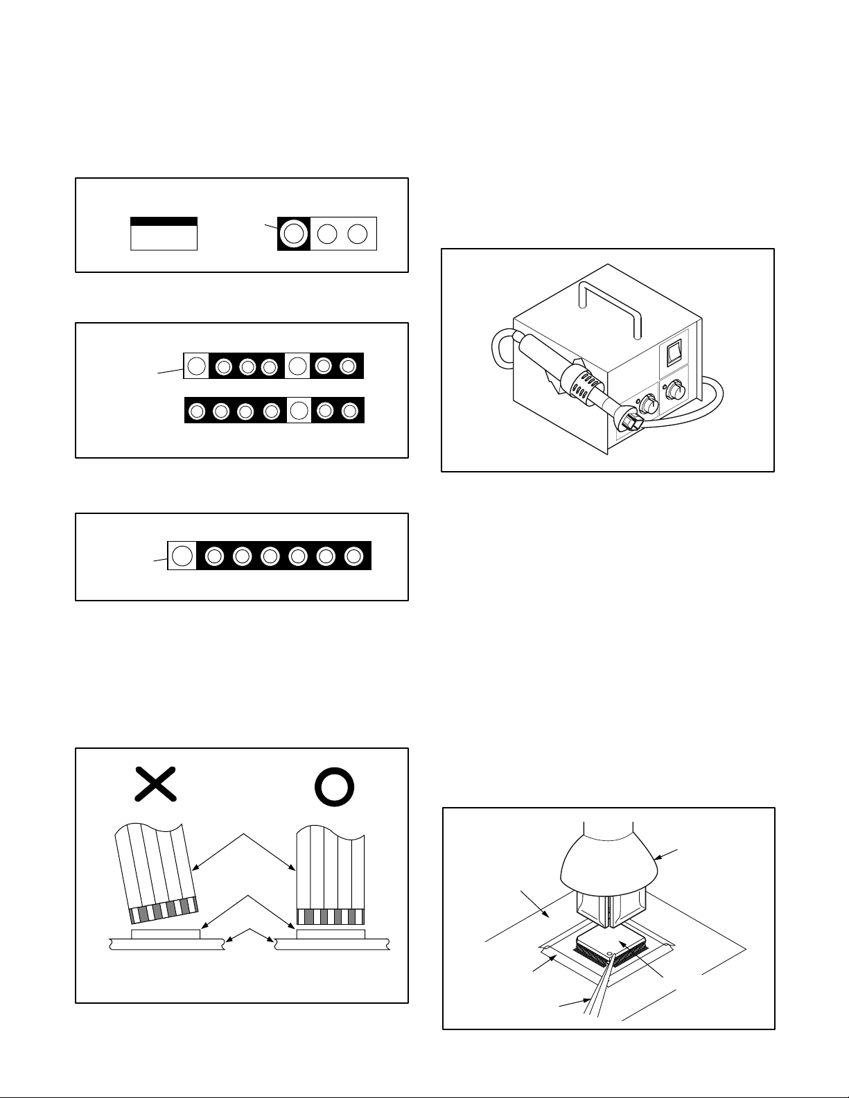
Hot-air
Flat Pack-IC
Desoldering
Machine
CBA
Flat Pack-IC
Tweezers
Masking
Tape
Fig. S-1-2
STANDARD NOTES FOR SERVICING
Circuit Board Indications
a. The output pin of the 3 pin Regulator ICs is indicated
as shown.
Top View
Out
b. For other ICs, pin 1 and every fifth pin are indicated
as shown.
Input
In
Bottom View
5
Pin 1
10
c. The 1st pin of every male connector is indicated as
shown.
Pin 1
Instructions for Connectors
1. When you connect or disconnect the FFC (Flexible
Foil Connector) cable, be sure to first disconnect the
AC cord.
2. FFC (Flexible Foil Connector) cable should be inserted parallel into the connector, not at an angle.
How to Remove / Install Flat Pack-IC
1. Removal
With Hot-Air Flat Pack-IC Desoldering Machine:
(1) Prepare the hot-air flat pack-IC desoldering ma-
chine, then apply hot air to the Flat Pack-IC (about 5
to 6 seconds). (Fig. S-1-1)
Fig. S-1-1
(2)Remove the flat pack-IC with tweezers while apply-
ing the hot air.
(3)Bottom of the flat pack-IC is fixed with glue to the
CBA; when removing entire flat pack-IC, first apply
soldering iron to center of the flat pack-IC and heat
up. Then remove (glue will be melted). (Fig. S-1-6)
(4)Release the flat pack-IC from the CBA using twee-
zers. (Fig. S-1-6)
Caution:
1. Do not supply hot air to the chip parts around the flat
pack-IC for over 6 seconds because damage to the
chip parts may occur. Put masking tape around the
flat pack-IC to protect other parts from damage.
(Fig. S-1-2)
2. The flat pack-IC on the CBA is affixed with glue, so
be careful not to break or damage the foil of each pin
or the solder lands under the IC when removing it.
FFC Cable
Connector
CBA
* Be careful to avoid a short circuit.
1-4-1
DVD_NOTE
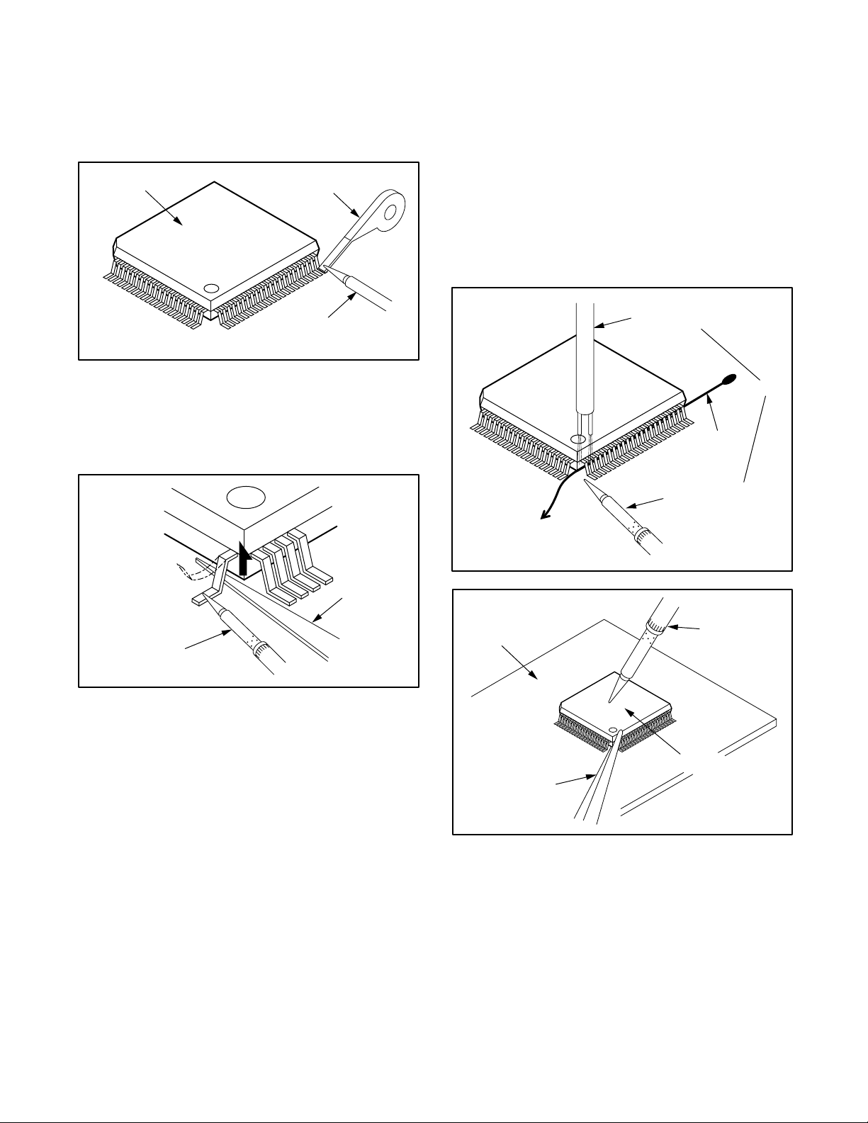
With Soldering Iron:
To Solid
Mounting Point
Soldering Iron
Iron Wire
or
Hot Air Blower
Fig. S-1-5
Fine Tip
Soldeing Iron
CBA
Flat Pack-IC
Tweezers
Fig. S-1-6
(1)Using desoldering braid, remove the solder from all
pins of the flat pack-IC. When you use solder flux
which is applied to all pins of the flat pack-IC, you can
remove it easily. (Fig. S-1-3)
Flat Pack-IC
(2)Lift each lead of the flat pack-IC upward one by one,
using a sharp pin or wire to which solder will not
adhere (iron wire). When heating the pins, use a fine
tip soldering iron or a hot air desoldering machine.
(Fig. S-1-4)
Desoldering Braid
Soldering Iron
Fig. S-1-3
(4)Bottom of the flat pack-IC is fixed with glue to the
CBA; when removing entire flat pack-IC, first apply
soldering iron to center of the flat pack-IC and heat
up. Then remove (glue will be melted). (Fig. S-1-6)
(5)Release the flat pack-IC from the CBA using twee-
zers. (Fig. S-1-6)
Note:
When using a soldering iron, care must be taken to
ensure that the flat pack-IC is not being held by glue.
When the flat pack-IC is removed from the CBA,
handle it gently because it may be damaged if force
is applied.
(3)Bottom of the flat pack-IC is fixed with glue to the
CBA; when removing entire flat pack-IC, first apply
soldering iron to center of the flat pack-IC and heat
up. Then remove (glue will be melted). (Fig. S-1-6)
(4)Release the flat pack-IC from the CBA using twee-
zers. (Fig. S-1-6)
With Iron Wire:
(1)Using desoldering braid, remove the solder from all
pins of the flat pack-IC. When you use solder flux
which is applied to all pins of the flat pack-IC, you can
remove it easily. (Fig. S-1-3)
(2) Affix the wire to a workbench or solid mounting point,
as shown in Fig. S-1-5.
(3)While heating the pins using a fine tip soldering iron
or hot air blower, pull up the wire as the solder melts
so as to lift the IC leads from the CBA contact pads
as shown in Fig. S-1-5.
Fine Tip
Soldering Iron
Sharp
Pin
Fig. S-1-4
1-4-2
DVD_NOTE
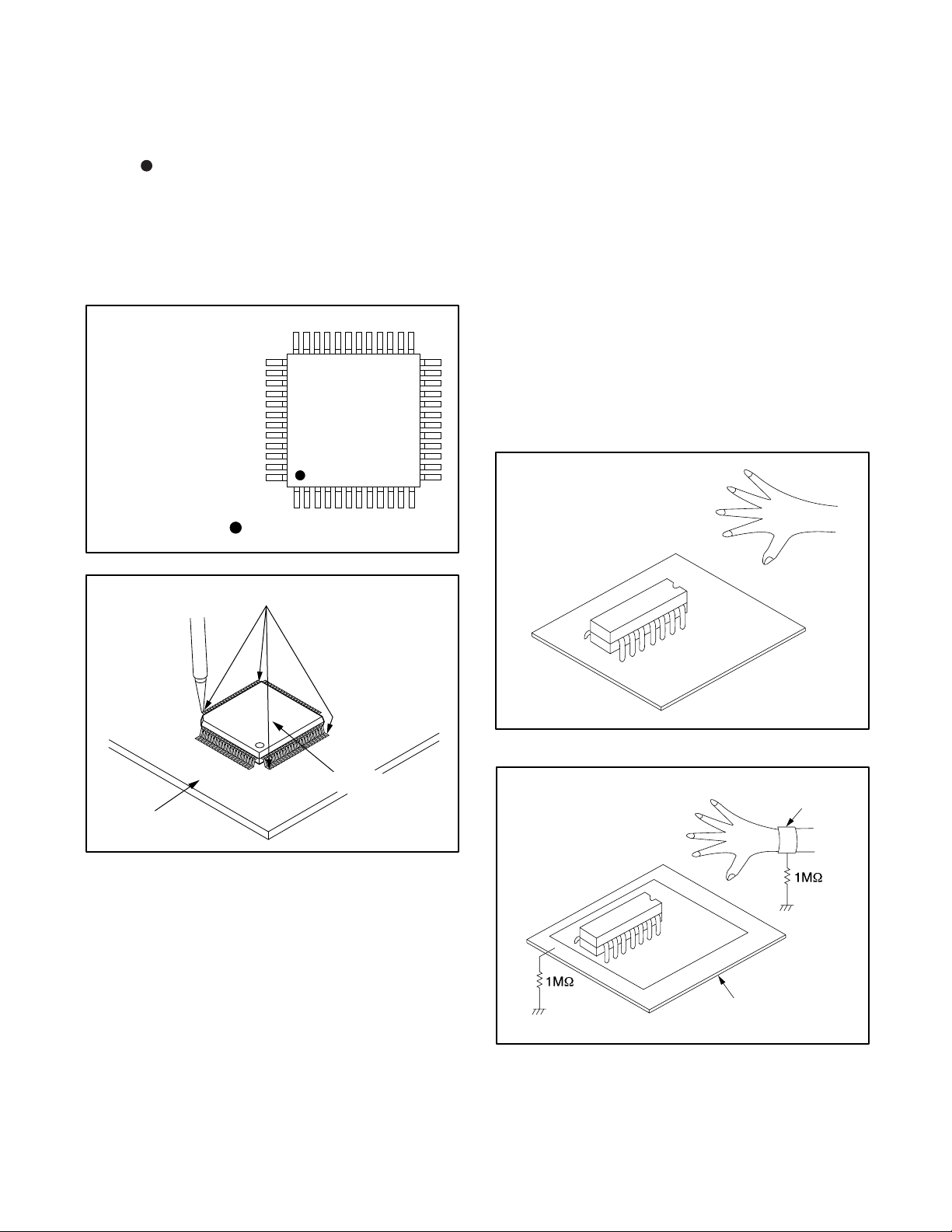
2. Installation
CBA
< Incorrect >
CBA
Grounding Band
Conductive Sheet or
Copper Plate
< Correct >
(1)Using desoldering braid, remove the solder from the
foil of each pin of the flat pack-IC on the CBA so you
can install a replacement flat pack-IC more easily.
(2) The “
(3)Solder all pins of the flat pack-IC. Be sure that none
” mark on the flat pack-IC indicates pin 1. (See
Fig. S-1-7.) Be sure this mark matches the 1 on the
PCB when positioning for installation. Then presolder the four corners of the flat pack-IC. (See Fig. S1-8.)
of the pins have solder bridges.
Instructions for Handling
Semi-conductors
Electrostatic breakdown of the semi-conductors may
occur due to a potential difference caused by electrostatic
charge during unpacking or repair work.
1. Ground for Human Body
Be sure to wear a grounding band (1MΩ) that is properly
grounded to remove any static electricity that may be
charged on the body.
2. Ground for Workbench
Example :
Pin 1 of the Flat Pack-IC
is indicated by a " " mark.
Presolder
Be sure to place a conductive sheet or copper plate with
proper grounding (1MΩ) on the workbench or other
surface, where the semi-conductors are to be placed.
Because the static electricity charge on clothing will not
escape through the body grounding band, be careful to
avoid contacting semi-conductors with your clothing.
Fig. S-1-7
CBA
Flat Pack-IC
Fig. S-1-8
1-4-3
DVD_NOTE
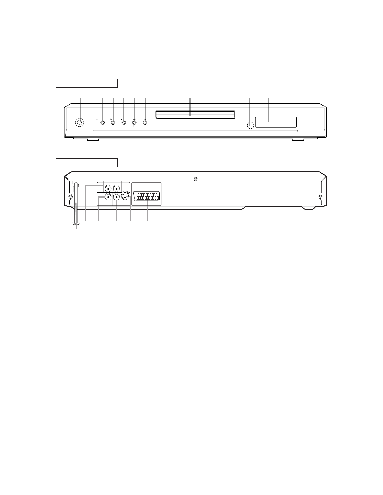
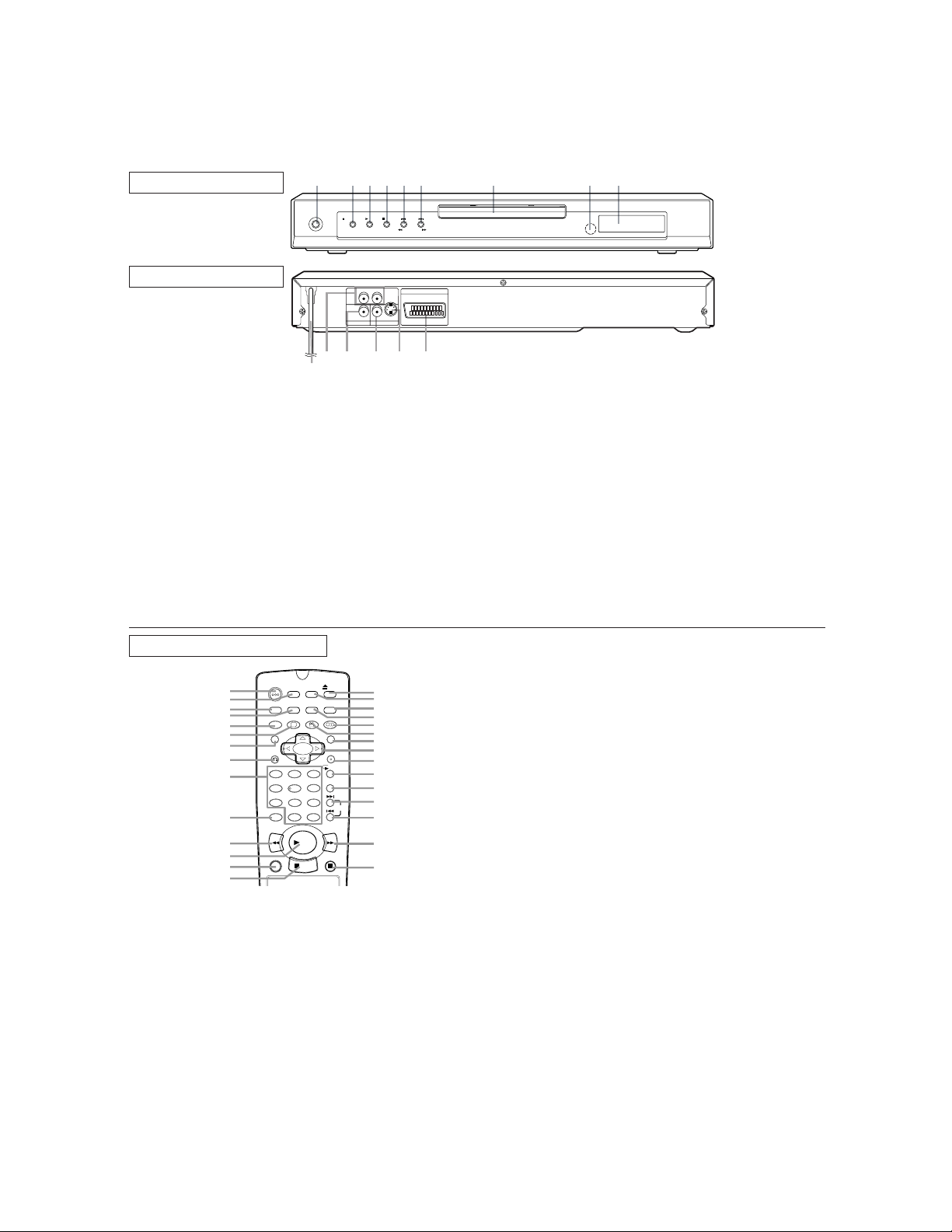
OPERATING CONTROLS AND FUNCTIONS
t
[ DV -SL10H ]
FRONT PANEL
243519876
OPERATE
OPEN/CLOSE PLAY STOP SKIP
REW FWD
REAR VIEW
RL
AUDIO OUT VIDEO OUT
12
13 14 1511
S-VIDEOVIDEODIGITAL
AV (TV)
10
1. OPERATE
to switch the player to ON or OFF
2. OPEN/CLOSE
to open/close the disc tray
3. PLAY
to start or resume disc playback
4. STOP
to stop playback
5. SKIP H / SEARCH h
goes to previous chapter or track during playback; press
and hold for 1.5 seconds for a reverse search
6. SKIP G / SEARCH g
goes to next chapter or track during playback; press and
hold for 1.5 seconds for a forward search
7. Disc tray
8. Remote sensor window
9. Display
10. MAIN (AC Power Cord)
connect to a standard AC outlet
11. AUDIO OUT (Left/Right)
connect to AUDIO inputs of an amplifier, receiver or
stereo system
12. DIGITAL (Digital audio out)
connect to AUDIO inputs of a digital (coaxial) audio
equipment
13. VIDEO OUT
connect to the Video Input of a TV
14. S-VIDEO OUT
connect to a TV with S-Video inputs
15. AV (TV)
connect SCART cable to a TV
Caution: Do not touch the inner pins of the jacks on the
rear
panel. Electrostatic discharge may cause permanen
damage to the player.
1-5-1
E5752IB
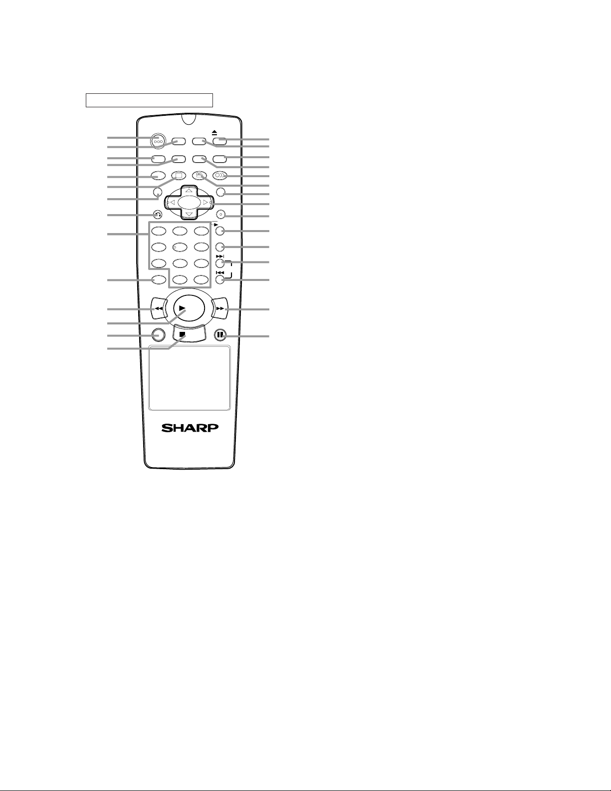
REMOTE CONTROL
s.
k
e
n
.
or
or
1
OPERATE
2
3
4
5
6
7
DIMMER
ZOOM
TITLE
RETURN
8
9
10
CLEAR
11
12
13
14
ON
SCREEN
GAMMA
SUBTITLE
1 2 3
54
7
8 9
C 0
REV
PLAY
STOP
SETUP
MARKER
MODE
ANGLE AUDIO
MENU
ENTER
A-B REPEAT
6
+
10
FWD
STILL/PAUSEDIRECT SKIP
OPEN/
CLOSE
REPEAT
SKIP
15
16
17
18
19
20
21
22
23
24
25
26
27
28
29
1. OPERATE Button
Press to turn the power on and off.
2. ON SCREEN Button
Displays the current status on the TV screen for checking purpose
3. DIMMER Button
Press to change the Panel Display settings.
4. GAMMA Button
Press to adjust the black parts of the picture brighter.
5. ZOOM Button
Enlarges part of a DVD-reproduced image.
6. SUBTITLE Button
Press to select a desired subtitle language.
7. TITLE Button
Displays the title menu.
8. RETURN Button
Returns to the previous operation.
9. Numeric Buttons
10. CLEAR Button
Resets a setting.
11. REV Button
Fast reverse playback to a desired point.
12. PLAY Button
Starts playback of the disc contents.
13. DIRECT SKIP Button
Press to locate a desired point.
14. STOP Button
Stops operation of the disc.
15. OPEN/CLOSE Button
Press to insert discs into or remove them from the tray.
16. SETUP Button
Press to enter the setup mode or to change setup items.
17. MARKER Button
Press to call back the Marker display.
18. MODE Button
Activates programme playback or random playbac
mode.(CD/MP3) Activates the 3D sound.(DVD)
19. AUDIO Button
Press to select a desired audio language or sound mode.
20. ANGLE Button
Press to change the camera angle to see the sequenc
being played back from a different angle.
MENU Button
21.
Displays the DVD menus.
22. Arrow Buttons
Use when making settings while watching the display o
a TV screen.
23. ENTER Button
Press to accept a setting.
24. REPEAT Button
Repeats playback of the current disc, title, chapter or track
25. A-B REPEAT Button
Repeats playback of a selected section.
26. SKIP UP Button
Plays back from the beginning of the next chapter
track.
27. SKIP DOWN Button
Plays back from the beginning of the current chapter
track.
28. FWD Button
Fast
forwards playback to a desired point.
29. STILL/PAUSE Button
Pause playback temporarily/frame-by-frame playback.
1-5-2
E5752IB
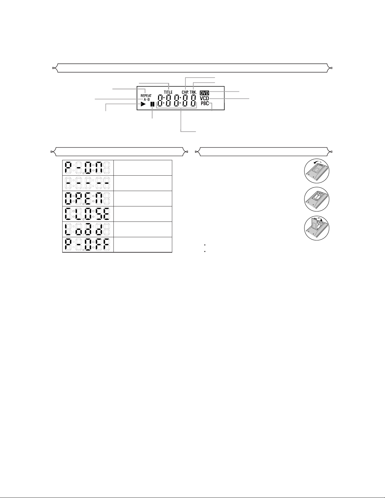
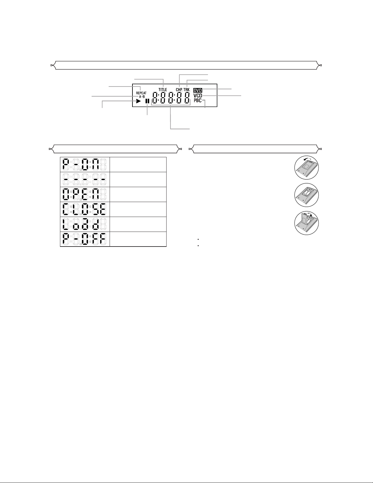
Display
4]
Stays on when
the repeat function is on.
Stays on when
the A-B repeat
function is on.
Stays on when the inserted
disc is being played back.
Stays on when repeat
title function is on.
Lights up when the
inserted disc comes
to a pause.
Stays on when repeat chapter function is on.
Stays on when repeat track function is on.
Lights up when a
playback control is
activated.
Displays how long a current title or track has been
played back. When a chapter or track has switched,
the number of a new title, chapter or track is displayed.
Lights up when a DVD
is inserted on the tray.
CD:
Lights up when a
CD is inserted on
the tray.
VCD:
Lights up when a
Video CD is
inserted on the tray.
[Fig.
Displays During Operation
Power on
No disc inserted or
playing DVD Menu
Tray open
Tray closed
Loading the Disc
Power off
Loading the Batteries
1. Open the battery compartment cover.
2. Insert two AA batteries, with each one
oriented correctly.
3. Close the cover.
NOTES
Do not mix alkaline and manganese batteries.
Do not mix old and new batteries.
1-5-3
E5752IB
[ DV-SL10S(Y)/DV-SL10S(R) ]
t
k
e
n
.
or
or
1
1
OPERATE
10
243519876
OPEN/CLOSE PLAY STOP SKIP
RL
S-VIDEOVIDEODIGITAL
AUDIO OUT VIDEO OUT
12 13 14 1511
REW FWD
AV (TV)
FRONT PANEL
REAR VIEW
1. OPERATE
to switch the player to ON or OFF
2. OPEN/CLOSE
to open/close the disc tray
3. PLAY
to start or resume disc playback
4. STOP
to stop playback
5. SKIP H / SEARCH h
goes to previous chapter or track during playback; press
and hold for 1.5 seconds for a reverse search
6. SKIP G / SEARCH g
goes to next chapter or track during playback; press and
hold for 1.5 seconds for a forward search
7. Disc tray
8. Remote sensor window
9. Display
10. MAIN (AC Power Cord)
connect to a standard AC outlet
11. AUDIO OUT (Left/Right)
connect to AUDIO inputs of an amplifier, receiver or
stereo system
12. DIGITAL (Digital audio out)
connect to AUDIO inputs of a digital (coaxial) audio
equipment
13. VIDEO OUT
connect to the Video Input of a TV
14. S-VIDEO OUT
connect to a TV with S-Video inputs
15. AV (TV)
connect SCART cable to a TV
Caution: Do not touch the inner pins of the jacks on the
rear panel. Electrostatic discharge may cause permanen
damage to the player.
REMOTE CONTROL
OPEN/
ON
OPERATE
1
2
DIMMER
3
4
5
6
7
8
9
10
ZOOM
TITLE
RETURN
1 2 3
7
CLEAR
C 0
REV
11
12
13
14
1. OPERATE Button
Press to turn the power on and off.
2. ON SCREEN Button
Displays the current status on the TV screen for checking purposes.
3. DIMMER Button
Press to change the Panel Display settings.
4. GAMMA Button
Press to adjust the black parts of the picture brighter.
5. ZOOM Button
Enlarges part of a DVD-reproduced image.
6. SUBTITLE Button
Press to select a desired subtitle language.
7. TITLE Button
Displays the title menu.
8. RETURN Button
Returns to the previous operation.
9. Numeric Buttons
0. CLEAR Button
Resets a setting.
1. REV Button
Fast reverse playback to a desired point.
SCREEN
GAMMA
SUBTITLE
54
8 9
PLAY
STOP
SETUP
MODE
MARKER
ANGLE AUDIO
6
+
10
STILL/PAUSEDIRECT SKIP
CLOSE
MENU
ENTER
REPEAT
A-B REPEAT
FWD
15
16
17
18
19
20
21
22
23
24
25
26
SKIP
27
28
29
12. PLAY Button
Starts playback of the disc contents.
13. DIRECT SKIP Button
Press to locate a desired point.
14. STOP Button
Stops operation of the disc.
15. OPEN/CLOSE Button
Press to insert discs into or remove them from the tray.
16. SETUP Button
Press to enter the setup mode or to change setup items.
17. MARKER Button
Press to call back the Marker display.
18. MODE Button
Activates programme playback or random playbac
mode.(CD/MP3) Activates the 3D sound.(DVD)
19. AUDIO Button
Press to select a desired audio language or sound mode.
20. ANGLE Button
Press to change the camera angle to see the sequenc
being played back from a different angle.
MENU Button
21.
Displays the DVD menus.
22. Arrow Buttons
Use when making settings while watching the display o
a TV screen.
23. ENTER Button
Press to accept a setting.
24. REPEAT Button
Repeats playback of the current disc, title, chapter or track
25. A-B REPEAT Button
Repeats playback of a selected section.
26. SKIP UP Button
Plays back from the beginning of the next chapter
track.
27. SKIP DOWN Button
Plays back from the beginning of the current chapter
track.
28. FWD Button
Fast forwards playback to a desired point.
29. STILL/PAUSE Button
Pause playback temporarily/frame-by-frame playback.
1-5-4
E5752IB
Display
Stays on when
the repeat function is on.
Stays on when
the A-B repeat
function is on.
Stays on when the inserted
disc is being played back.
Stays on when repeat
title function is on.
Lights up when the
inserted disc comes
to a pause.
Stays on when repeat chapter function is on.
Stays on when repeat track function is on.
Lights up when a
playback control is
activated.
Displays how long a current title or track has been
played back. When a chapter or track has switched,
the number of a new title, chapter or track is displayed.
Lights up when a DVD
is inserted on the tray.
CD:
Lights up when a
CD is inserted on
the tray.
VCD:
Lights up when a
Video CD is
inserted on the tray.
Displays During Operation
Power on
No disc inserted or
playing DVD Menu
Tray open
Tray closed
Loading the Disc
Power off
Loading the Batteries
1. Open the battery compartment cover.
2. Insert two AA batteries, with each one
oriented correctly.
3. Close the cover.
NOTES
Do not mix alkaline and manganese batteries.
Do not mix old and new batteries.
1-5-5
E5752IB
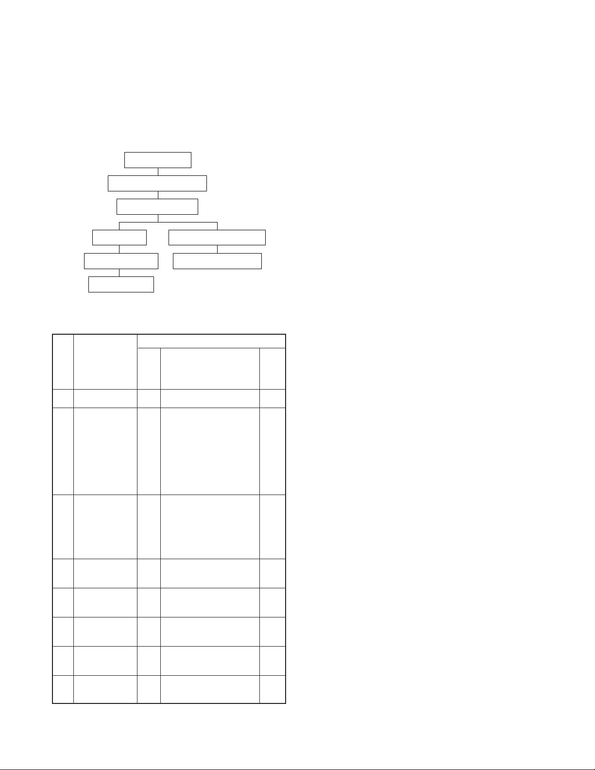
CABINET DISASSEMBLY INSTRUCTIONS
1. Disassembly Flowchart
This flowchart indicates the disassembly steps to gain
access to item(s) to be serviced. When reassembling,
follow the steps in reverse order. Bend, route, and dress
the cables as they were originally.
[1] Top Cover
[2] Front Assembly
[3] DVD Mecha
[5] DVD Main CBA Unit[4] AV CBA
1 : Identification (location) No. of parts in the figures
2 : Name of the part
3 : Figure Number for reference
4 : Identification of parts to be removed, unhooked,
unlocked, released, unplugged, unclamped, or desoldered.
P=Spring, L=Locking Tab, S=Screw,
CN=Connector,
*=Unhook, Unlock, Release, Unplug, or Desolder
e.g.5(S-1) = five Screws (S-1),
2(L-2) = two Locking Tabs (L-2)
5 : Refer to "Reference Notes."
[7] Main CBA Holder[6] Function CBA
[8] Rear Panel
2. Disassembly Method
ID/
LOC.
No.
[1] Top Cover 1 5(S-1) [2] Front 2 *2(L-1), Tray Panel, 1-1
[3] DVD 3,4 3(S-2) 2
[4] AV CBA 5 3(S-3), 3(S-4), -
[5]
[6]
[7] Main CBA 6 (S-6) -
[8] Rear 6 (S-7) -
↑↑↑ ↑ ↑
123 4 5
PART
Assembly *2(L-2), *5(L-3), 1-2
Mecha *CN301, *CN201 2-1
DVD
Main 5 2(S-5) -
CBA Unit
Function
CBA
Holder
Panel
Fig.
No.
5 Desolder -
REMOVAL
REMOVE/
*UNHOOK/UNLOCK/
RELEASE/UNPLUG/
DESOLDER
*3(L-4) 1-3
*CN1001, *CN1601
Note
1-4
1-5
1-6
1-7
2-2
2-3
3
Reference Notes
CAUTION 1: Locking Tabs (L-1), (L-2), (L-3) and (L-4)
are fragile. Be careful not to break them.
1-1. Connect the wall plug to an AC outlet and press the
OPEN/CLOSE button to open the Tray.
1-2. Remove the Tray Panel by releasing two Locking
Tabs (L-1).
1-3. Press the OPEN/CLOSE button again to close the
Tray.
1-4. Press the POWER button to turn the power off.
1-5. Unplug an AC Cord.
1-6. Release two Locking Tabs (L-2). Then, release
five Locking Tabs (L-3) (to do this, first release two
Locking Tabs (A) at the side, and then three
Locking Tabs (B) at the bottom.) (Fig. 2)
1-7. Release three Locking Tabs (L-4). Then remove
the Front Assembly.
CAUTION 2: Electrostatic breakdown of the laser diode
in the optical system block may occur as a potential
difference caused by electrostatic charge accumulated
on cloth, human body etc., during unpacking or repair
work.
To avoid damage of pickup follow next procedures.
2-1. Disconnect Connector (CN301). Remove three
Screws (S-2) and lift the DVD Mecha. (Fig. 3)
2-2. Slide the pickup unit front.
2-3. Short the three short lands with solder before
removing the FFC cable (CN201) from it. If you
disconnect the FFC cable (CN201), the laser diode
of pickup will be destroyed. (Fig. 4)
CAUTION 3: When reassembling, confirm the FFC
cable (CN201) is connected completely. Then remove
the solder from the three short lands of FPC cable.
(Fig. 4)
1-6-1
E5752DC
View for B
Pickup Unit
C
B
Short the three short
lands by soldering
Short the three short lands by soldering
FPC Cable
Connector
Slide
DVD Mecha
View for C
View for A
OR
A
(S-1)
(L-1)
(A)
(L-4)
[1] Top Cover
(S-1)
(S-1)
Fig. 1
Tray Panel
(L-2)
(L-1)
(L-4)
(L-3)
(B)
(L-3)
(S-2)
CN301
CN201
[2] Front Assembly
(A)
Fig. 2
(S-2)
Fig. 4
[3] DVD Mecha
Fig. 3
1-6-2
E5752DC

(S-7)
[8] Rear
Panel
(S-6)
[7] Main CBA
Holder
)
[6] Function CBA
(S-5)
[5] DVD Main
CBA
[4] AV CBA
CN1601
CN1001
Desolder
from
bottom
Fig. 5
(S-4)
(S-4)
(S-3
Fig. 6
HOW TO MANUAL EJECT
1. Remove the Top Cover.
2. Rotate the roulette in the direction of the arrow as
shown below.
A
View for A
Rotate this roulette in
the direction of the arrow
1-6-3
E5752DC
TEST MODE
>
>
Test Mode
ROM Renewal Mode
[TEST MODE]
Test Mode Initial Display (Fig.T-1)
Displaying F/W Ver.
Displaying VFD F/W Ver.
A power source is put, and [1], [2], [3], [4], and [ON SCREEN] buttons on the remote
control unit are pushed in that order while the tray is opening or after the “NO DISC”
display at the same time.
A power source is put, and [9], [8], [7], [6], and [DIRECT SKIP] buttons on the remote
control unit are pushed in that order while the tray is opening or after the “NO DISC”
display at the same time.
Test Mode Flow Chart
< Press 1 button on the remote control unit. >
All VFD ON/OFF
Menu Display (Fig. T-2)
Displaying VFD "TEST1"
< Press 1 button on the remote control unit.
All VFD ON
< Press 2 button on the remote control unit.
All VFD OFF
< Press RETURN button on
the remote control unit. >
Returning to Test Mode Initial Display
< Press 3 button on the remote control unit. >
Cearing FLASH MEMORY (Fig. T-3)
Displaying VFD "TEST3"
1-7-1
TESTMODE
(model name) VERSION REGION
.
1. TEST1-VFD
2. TEST2-REPEAT PLAY
3. TEST3-EEPROM CLEAR
4. TEST4-MEASUREMENT SERVO
5. TEST5-DISC READ CHECK
6. TEST6-MECHA CHECK
7. TEST7-DISC INFO
8. TEST8-ERROR RATE
POWER
EXIT:
Fig. T-1: Test Mode Initial Display
(model name) VERSION REGION
.
TEST1-VFD
1. ON
2. OFF
VFD STATUS [---]
POWERRETURN
RETURN:
EXIT:
Fig. T-2: All VFD ON/OFF Menu Display
(model name) VERSION REGION
.
TEST3-EEPROM CLEAR
EEPROM CLEAR : OK
POWER
EXIT:
Fig. T-3: Clearing FLASH MEMORY Display
1-7-2
TESTMODE
[ROM RENEWAL MODE]
F
e
F
e)
F
e)
1. Turn the power on and remove the disc on the tray.
2. To put the DVD player into version up mode, press
[9], [8], [7], [6], and [DIRECT SKIP] buttons on the
remote control unit in that order. The tray will open
automatically.
Fig. a appears on the screen and Fig. b appears on
the VFD.
F/W Version Up Mode
VERSION : ********
Completed
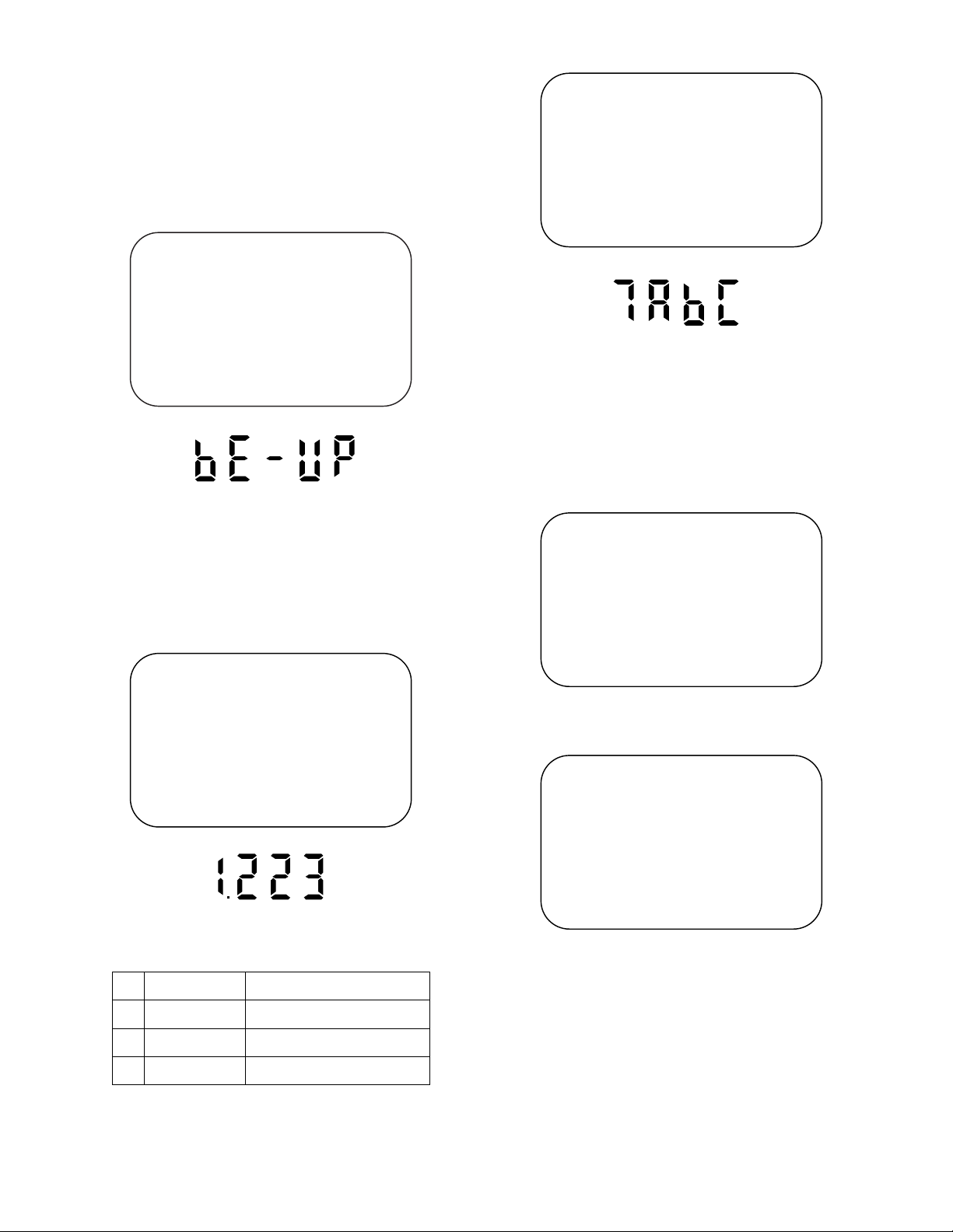
SUM : 7abc (*3)
F/W Version Up Mode
Please insert a DISC
for F/W Version Up.
EXIT: POWER
Fig. a Version Up Mode Screen
ig. b VFD in Version Up Mod
The DVD player can also enter the version up mode
with the tray open. In this case, Fig. a will be shown
on the screen while the tray is open.
3. Load the disc for version up.
4. The DVD player enters the F/W version up mode
automatically. Fig. c appears on the screen and
Fig. d appears on the VFD.
F/W Version Up Mode
VERSION : ********
Reading...(*2)
Fig. e Completed Program Mode Screen
ig. f VFD upon Finishing the Programing Mode (Exampl
At this time, no buttons are available.
6. Unplug the AC cord from the AC outlet. Then plug it
again.
7. Turn the power on by pressing the power button and
the tray will close.
8. Press [1], [2], [3], [4], and [DIRECT SKIP] buttons on
the remote control unit in that order.
Fig. g appears on the screen.
model: ****** Ver: **** Region: **
1: VFD TEST
2: TT REPEAT PLAY
3: EEPROM CLEAR
4: MEASUREMENT SERVO
5: DISC READ CHECK
6: MECHA CHECK
7: DISC INFO
8: ERROR RATE
EXIT: POWERRETURN: -----
Fig. g
9. Press [3] button on the remote control unit.
Fig. h appears on the screen.
model: ****** Ver: **** Region: **
EXIT: POWER
TEST 3: EEPROM CLEAR
EEPROM CLEAR: OK
Fig. c Programming Mode Screen
ig. d VFD in Programming Mode (Exampl
The appearance shown in (*2) of Fig. c is described
as follows:
AppearanceNo. State
Reading... Sending files into the memory
1
Erasing... Erasing previous version data
2
Programming...
3 Writing new version data
Fig. H
10.To finish this mode, press [POWER] button.
EXIT: POWERRETURN: -----
5. After programming is finished, the tray opens automatically. Fig. e appears on the screen and the
checksum in (*3) of Fig. e appears on the VFD. (Fig. f)
1-7-3
TESTMODE

[ ERROR RATE MEASUREMENT]
1
2
3
4
1. Turn on the power to the player, remove the disk
from the tray, and close the tray.
2. To put the DVD player into test mode, press [1], [2],
[3], [4], and [ON SCREEN] buttons on the remote
control unit in that order.
The unit will switch to Test Mode and Fig. a will be
displayed. For VFD, the current F/W version will be
displayed. (Fig. b)
(model name) VERSION REGION
1. TEST1-VFD
2. TEST2-REPEAT PLAY
3. TEST3-EEPROM CLEAR
4. TEST4-MEASUREMENT SERVO
5. TEST5-DISC READ CHECK
6. TEST6-MECHA CHECK
7. TEST7-DISC INFO
8. TEST8-ERROR RATE
Fig. a Test Mode Screen
Fig. b Sample VFD in Test Mode
3. Press the [8] button to select "8. TEST 8 - ERROR
RATE." The on-screen display will change to the
screen shown in Fig. c. The VDF display will change
to the display shown in Fig. d.
(model name) VERSION REGION
TEST8-ERROR RATE
DISC:DVD-V / DUAL LAYER / OPPOSITE
STA:
STATUS:
CHECK : OK
NOW MEASURE : L
Uncorrect
Correct
RETURN:
H /2HH/
1
PO1st
00000 00000 00000 00000 00000
00000 00000 00000 00000 00000
(I) With a DVD inserted.
(model name) VERSION REGION
TEST8-ERROR RATE
DISC: CD
STA:
STATUS:
CHECK : OK
NOW MEASURE :
H TRK : :
C1 Correct
C2 Uncorrect
RETURN:
(II) With a CD/VCD inserted.
Fig. c TEST8-ERROR RATE MODE
.
POWER
EXIT:
.
H /4H
3
5
PI1st PO2nd PO3rdPI2nd
POWERRETURN
EXIT:
.
5
: :
00000
00000
POWERRETURN
EXIT:
4. Put disk to be checked into the tray. Close the tray
using either the [OPEN/CLOSE] or [PLAY] button on
the unit or on the remote. The disk will automatically
be distinguished and error rate measurement will
begin.
Fig. c will display:
Inserted disk’s inner parameter (For DVD, Layer
0, initial address)
Inserted disk’s outer parameter (For DVD, Layer
0, final address)
Inserted disk’s Layer 1, initial address.
Inserted disk’s Layer 1, final address.
Depending on the contents of the inserted disk, 3
and 4 above may not be displayed.
Once the error rate measurement has started, if the
largest value resulting from the first three measurements has a value of 2000 or less, and all values in
the "Uncorrect" row are 0, the message "CHECK :
OK" will be displayed on area 5.
If the largest value is greater than 2000, the message "CHECK : NG" will be displayed on area 5.
The message "OK" or "NG" will continue to be
displayed without change until the measurement is
stopped. The error rate measurement will continue
to be updated.
5. "Correct" and "Uncorrect" in Fig. c:
(1)For DVDs the following will be displayed:
PO1st-Correct count; PO1st-Uncorrect count;
PI1st-Correct count; PI1st-Uncorrect count;
PO2nd-Correct; PO2nd-Uncorrect count;
PI2nd-Correct count; PI2nd-Uncorrect count;
PO3rd-Correct count; PO3rd-Uncorrect count.
The above ten numerical values will be displayed for
each 80 ECC block.
(2)For CD/VCDs the following will be displayed:
C1-Correct count; C2-Uncorrect count.
The values for these two items will be displayed
every 7350x4 frames.
For VFD, the following will be displayed:
PO1st-Correct count; (C1-Correct count for CDs).
(Fig. e)
Fig. e: Sample VFD display of ERROR RATE
measurement
6. To end the ERROR RATE measurement, press the
[OPEN/CLOSE] button on either the unit or the
remote. After the display has ceased, press the
[POWER] button on either the unit or the remote to
shut off the power.
Fig. d Sample VFD in TEST8-ERROR RATE MODE
1-7-4
TESTMODE
FLOW CHART NO.1
t
The power cannot be turned on.
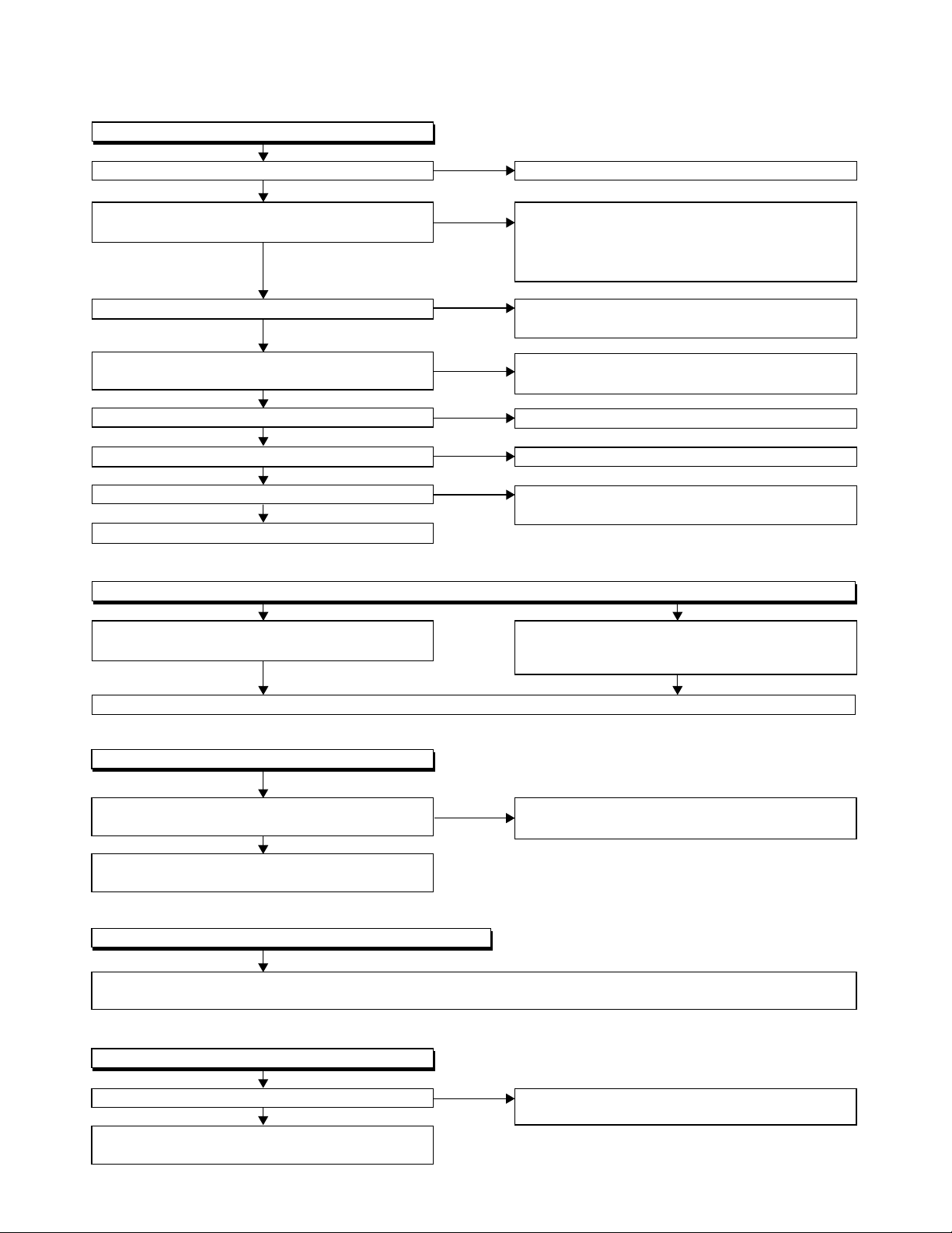
TROUBLESHOOTING
Is the fuse normal?
Yes
Is normal state restored when once unplugged
power cord is plugged again after several seconds?
Yes
Is each voltage of the secondary side normal?
Yes
When pressing POWER button (SW2001), is the
voltage of 0V supplied to pin(8) of IC2002?
Yes
Is the voltage of 5V supplied to pin(1) of IC2002?
Yes
Is the voltage of 3.3V outputted to pin(19) of CN1001?
Yes
Is the voltage of 0V supplied to pin(18) of IC2002?
Yes
Replace IC2002.
FLOW CHART NO.2
The fuse blows out.
No
No
No
No
No
No
See FLOW CHART No.2 <The fuse blows out.>
Check if there is any leak or shor-circuiting on the
primary circuit component.
(Q1001, Q1003, T1001, D1001, D1002, D1004,
D1005, D1011, C1003, C1005)
Check each rectifying circuit of the secondary circui
and service it if defective.
Check POWER button (SW2001) and their
periphery, and service it if defective.
Check EV+5V line
Replace DVD Main CBA unit.
Check Q2007 and their periphery, and service it if
defective.
and service it if defective.
Check the presence that the primary component
is leaking or shorted and service it if defective.
After servicing, replace the fuse.
FLOW CHART NO.3
When the output voltage fluctuates.
Does the photo coupler circuit on the secondary
side operate normally?
Yes
Check IC1001, D1012, D1024 and their periphery,
and service it if defective.
FLOW CHART NO.4
When buzz sound can be heard in the vicinity of power circuit.
Check if there is any short-circuit on the rectifying diode and the circuit in each rectifying circuit of the secondary side,
and service it if defective. (D1003, D1006, D1008, D1016, D1030, IC1002, Q1002, Q1004, Q1010, Q1011, Q1014, Q1050)
FLOW CHART NO.5
-FL is not outputted.
No
Check the presence that the rectifying diode or
circuit is shorted in each rectifying circuit of
secondary side, and service it if defective.
Check IC1001, IC1006, D1015, D1048 and their
periphery, and service it if defective.
Is -24V voltage supplied to the anode of D1003?
Yes
Check if there is any leak or short-circuit
on the loaded circuit, and service it if defective.
No
1-8-1
Check D1003 and periphery circuit, and service it
if defective.
E5752TS

.
FLOW CHART NO.6
.
P-ON+12V is not outputted.
Is 12V voltage supplied to the emitter of Q1002?
Yes
Is the voltage of base on Q1002 lower than the
voltage of emitter on Q1002 when turning the power on?
Yes
Replace Q1002.
FLOW CHART NO.7
EV+9V is not outputted.
Is 9V voltage supplied to the collector of Q1050?
Yes
Is the "H" pulse inputted into the base of Q1050?
Yes
Replace Q1050.
FLOW CHART NO.8
P-ON+5V is not outputted. (EV+9V is outputted normally.)
Is the "H" pulse inputted into the base of Q1004?
Yes
Replace Q1004.
No
No
No
No
No
Check D1030, D1048, L1009, C1035, C1048 and
the periphery circuit, and service it if defective.
Check Q1016 and PWRCON line and service it if
defective.
Check D1030, D1048, L1009, C1035, C1048, R1097
and the periphery circuit, and service it if defective.
Check D1072, C1070, R1098 and service it if
defective.
Check R1068 and D1046, and service it if defective
FLOW CHART NO.9
P-ON+3.3V is not outputted. (P-ON+12V is outputted normally.)
Is 3.3V voltage supplied to the collector of Q1011?
Yes
Replace Q1011 and R1067.
FLOW CHART NO.10
EV+3.3V is not outputted.
Is 3.3V voltage supplied to the emitter of Q1010?
Yes
Is the "L" pulse inputted into the base of Q1012?
Yes
Check Q1012, Q1010, R1087 and R1088,
and service it if defective.
FLOW CHART NO.11
EV+5V is not outputted.
Is EV+9V outputted normally?
Yes
Is the "H" pulse inputted into the base of Q1014?
Yes
Replace Q1014.
No
No
No
No
No
Check D1008, D1015, C1007, C1038 and the
periphery circuit, and service it if defective.
Check D1008, D1015, C1007, C1038 and the
periphery circuit, and service it if defective.
Is the "L" pulse outputted to Pin(19) of IC2002?
Yes No
Check the circuit between
Pin(19) of IC2002 and Q1012,
and service it if defective.
Refer to "FLOW CHART NO.7"
<EV+9V is not outputted.>
Check D1047, R1069, and service it if defective.
Replace IC2002
1-8-2
E5752TS

.
.
e.
.
FLOW CHART NO.12
.
EV+1.5V is not outputted.
Is 2.5V voltage supplied to Pin(1) of IC1002?
Yes
Is 1.25V voltage supplied to Pin(4) of IC1002?
Yes
Replace IC1002.
FLOW CHART NO.13
The fluorescent display tube does not light up.
Is the voltage of 3.3V supplied to Pin(6) and
Pin(24) of IC2001?
Yes
Is the voltage of -24V supplied to Pin(15) of
IC2001?
Yes
Is there 500kHz oscillation at Pin(26) of IC2001?
Yes
Check the signal lines of FP-DIN, FP-DOUT,
FP-CLK, FIP-STB of IC2001 and CN1001?
Yes
Are the filament voltage supplied between
Pins(1, 2) and Pins(34, 35) of the fluorescent
display tube? And the negative voltage applied
between these pins and GND?
Yes
Replace the fluorescent display tube.
FLOW CHART NO.14
The key operation is disabled.
No
No
No
No
No
No
No
Check D1006, C1014 and the periphery circuit.
Is the "L" pulse outputted to Pin(19) of IC2002?
Yes No
Check the circuit between Pin(19)
of IC2002 and Pin(4) of IC1002
Replace IC2002
,
and service it if defective.
Check the EV+3.3V line, and service it if defective
Check the -FL (-24V) line, and service it if defective
Check R2015, IC2001 and their periphery, and
service it if defective.
Check or replace IC2001 and its periphery, and
DVD Main CBA unit, and service it if defective.
Check or replace the power circuit, D1016, D1017,
T1001, and their periphery, and service it if defective
No
Is the voltage of -17V supplied to the collector of
Q1005?
Yes
Is the "H" signal inputted
at base of Q1016?
Yes
Check PWRCON line,
and service it if defectiv
No
Check or replace Q1015, Q1016, D1055, and
their periphery
, and service it if defective.
Is key switch contact (SW2001-SW2003, 2005,
2006, 2008) and installation state normal?
Yes
Is the control voltage normally inputted into
Pins(7, 8) of IC2002?
Yes
Replace IC2002.
No
No
1-8-3
Service or replace some poor switches.
Check the key switches (SW2001-SW2003, 2005,
2006, 2008), and their periphery circuit
, and
service it if defective.
Terminal voltage of IC2002-7,8
4.10
3.20
2.42
1.49
0.49
(V)
KEY-1
IC2002-7
-----
STOP
PAUSE
SKIP-UP
SKIP-DOWN
KEY-2
IC2002-8
-----
-----
PLAY
OPEN/CLOSE
POWER
E5752TS

FLOW CHART NO.15
.
No operation is possible from the remote control unit.
Operation is possible from the DVD, but no
operation is possible from the remote control unit.
Yes
Is no operation possible if replacing the remote
control unit?
Yes
Is 5V voltage supplied to the Pin(3) terminal of
the infrared remote control receiver?
Yes
Is the "L" pulse sent out Pin(1) terminal of receiver
when the infrared remote control is activated?
Yes
Is the "L" pulse signal supplied to the Pin(20) of
IC2002 when the infrared remote control is activated?
Yes
Replace DVD Main CBA unit.
FLOW CHART NO.16
The disc tray cannot be opened and closed.
(It can be done using the remote control unit.)
No
No
No
No
Original remote control unit is poor.
Check EV+5V line
Replace the infrared remote control receiver.
Replace IC2002.
, and service it if defective.
Is 0.49V to 1.49V voltage inputted into Pin(8) of
IC2002 when the "OPEN/CLOSE" button is activated?
Yes
See FLOW CHART NO. 17. <The disc tray cannot be opened and closed.>
FLOW CHART NO.17
The disc tray cannot be opened and closed.
Is the "L" pulse sent out Pin(20) of IC2002
when the "OPEN/CLOSE" button is activated?
Replace the DVD Main CBA Unit.
No improvement can be found.
Yes
Replace the DVD Mecha.
FLOW CHART NO.18
[No Disc] indicated. (When the focus error occurs.)
Replace the DVD Main CBA.
No
No
No
Check the SW2005 and "OPEN/CLOSE" button,
and service it if defective.
Replace IC2002.
The malfunction of the original DVD Main CBA Unit
No improvement can be found.
Yes
Replace the DVD Mecha.
No
1-8-4
Original DVD Main CBA is poor.
E5752TS

FLOW CHART NO.19
[No Disc] indicated. (When the focus servo is not functioning.)
Replace the DVD Main CBA.
No improvement can be found.
Yes
Replace the DVD Mecha.
FLOW CHART NO.20
[No Disc] indicated. (When the laser beam does not light up.)
Replace the DVD Main CBA.
No improvement can be found.
Yes
Replace the DVD Mecha.
FLOW CHART NO.21
Both functions of picture and sound do not operate normally.
Replace the DVD Main CBA.
No improvement can be found.
Yes
Replace the DVD Mecha.
No
No
No
Original DVD Main CBA is poor.
Original DVD Main CBA is poor.
Original DVD Main CBA is poor.
1-8-5
E5752TS

FLOW CHART NO.22
Picture does not appear normally.
Set the disc on the disc tray, and playback.
Are the video signals outputted to each pin of
CN1601 on the AV CBA?
CN1601 1PIN S-Y
CN1601 9PIN S-C
CN1601 7PIN G
CN1601 5PIN B
CN1601 3PIN R
Yes
Are the video signals shown above inputted into
each pin of IC1401?
IC1402 6PIN S-Y
IC1402 2PIN S-C
IC1402 16PIN G
IC1402 12PIN B
IC1402 14PIN R
Yes
Are the video signals outputted to each pin
of IC1401?
IC1402 31PIN CVBS
IC1402 28PIN S-Y
IC1402 33PIN S-C
IC1402 19PIN G
IC1402 25PIN B
IC1402 22PIN R
Yes
Are the video signals outputted to the specific
output terminal?
Are the luminance signals outputted to the
S-OUT terminal (JK1401)?
Are the chroma signals outputted to the
S-OUT terminal (JK1401)?
Are the component video signals outputted to the
VIDEO OUT terminal (JK1404)?
Are the composite video signals outputted to
the VIDEO OUT terminal (JK1402, JK1404)?
No
No
No
No
No
No
No
Replace the DVD Main CBA or DVD Mecha.
Check the line between each pin of CN1601 and
each pin of IC1401 on the AV CBA, and service it
if detective.
CN1601 1PIN → IC1402 6PIN S-Y
CN1601 9PIN → IC1402 2PIN S-C
CN1601 7PIN → IC1402 16PIN G
CN1601 5PIN → IC1402 12PIN B
CN1601 3PIN → IC1402 14PIN R
Is 5V voltage applied to the pin(1, 24) of
IC1401?
Yes No
Replace IC1401. Check P-ON+5V line and
service it if detective.
Check the periphery of JK1401 from
Pin (28) of IC1401 and service it if detective.
Check the periphery of JK1401 from
Pin (33) of IC1401 and service it if detective.
Check the periphery of JK1404 from Pins (19, 22,
25) of IC1401 and service it if detective.
Check
the periphery of JK1402 and JK1404
Pin(31) of IC1401
and service it if detective.
from
1-8-6
E5752TS

FLOW CHART NO.23
Audio is not outputted.
Set the disc on the disc tray, and playback.
Are the analog audio signals outputted to each pin
of CN1601 on AV CBA?
CN1601 13PIN AUDIO-L
CN1601 15PIN AUDIO-R
Yes
Are the analog audio signals inputted to each pin
of IC1201?
IC1201 2PIN AUDIO-L
IC1201 6PIN AUDIO-R
Yes
Is the "H" level mute signal outputted to CN1601
on AV CBA ?
CN1601 12PIN A-MUTE
CN1601 16PIN A-R-MUTE
CN1601 14PIN A-L-MUTE
Yes
Are the analog audio signals inputted to each pin
of IC1201?
IC1201 1PIN AUDIO-L
IC1201 7PIN AUDIO-R
Yes
Are the audio signals outputted to the specific
output terminal?
Are the audio signals outputted to the audio
terminal (JK1402)?
No
No
No
No
No
Replace the DVD Main CBA or DVD Mecha.
Check each line between each pin of CN1601
and each pin of IC1201 on AV CBA, and service it
if detective.
CN1601 13PIN → IC1201 2PIN AUDIO-L
CN1601 15PIN → IC1201 6PIN AUDIO-R
Replace the DVD Main CBA or DVD Mecha.
Replace IC1201.
Check the periphery between Pins(1,7) of IC1201
and JK1402, and service it if detective.
1-8-7
E5752TS

System Control/Servo Block Diagram
BLOCK DIAGRAMS
TO
VIDEO/ AUDIO
BLOCK DIAGRAM
FOCUS SERVO SIGNAL TRACKING SERVO SIGNAL
IC451
(CLOCK GENERATOR)
3
15
10
PCM-SCLK
A-MUTE
ADAC-MD
ADAC-MC
ADAC-ML
ASPECT
MULTI
1/4
PLL
1/4
PLL2
IC301
(SERVO DRIVE)
SLED SERVO SIGNAL SPINDLE SERVO SIGNAL
IC101
(MICRO CONTROLLER)
EXT CLOCK
172
CLK33M
BE CLOCK
170
X451
X'TAL
OSC
7
8
14
36.864MHz
OSC
1792FSEL
95
A-MUTE
ADAC-MD
51
50 ADAC-MC
96 ADAC-ML
64 ASPECT
FP-STB
FP-DOUT
FP-CLK
REMOTE
PWRCON
59
54FP-DIN
55
53
61
63
CN401
16 FP-STB 16
18 FP-DIN 18
20 FP-DOUT 20
21 FP-CLK 21
22 REMOTE 22
19 PWRCON 19
CN1001
IC2001
(FRONT PANEL CONTROL)
1G
23
2
FP-STB
28
FP-DIN
27
FP-DOUT
1
FP-CLK
7G
~~
17
a
h
14
16
i
FL2001
~
GRID FIP
7
~
SEGMENT
SPINDLE
MOTOR
M
SLED
MOTOR
M
FG CBA
FG
SENSOR
TRAY-OUT
TRAY-IN
TO DIGITAL SIGNAL
PROCESS BLOCK
DIAGRAM
DRIVE CBA
FS(+)
FS(-)
TS(+)
TS(-)
CN301
3SP(+)
4SP(-)
5TRAY-OUT
6TRAY-IN
7GND
8SL(-)
9SL(+)
1FG-IN
FOCUS
15
ACTUATOR
DRIVE
16
TRACKING
14
ACTUATOR
DRIVE
13
SPINDLE
12
MOTOR
DRIVE
11
SLED
17
MOTOR
DRIVE
18
IC202
(OP AMP)
12 14
27
+
-+
-
+
-
+
-
+
-
+3.3V
26
25
24
+
-
1
2
3
4
+
-
5
6
23
IC461
5 4
DVD MAIN CBA
152
FOCUS DRIVE
TRACKING
150
DRIVE
SPDL71
SLD70
RESET68RESET
TRAY-OUT
97
TRAY-IN
60
FG-IN
66
RM2001
REMOTE
SENSOR
Q2007
IC2002
ENERGY STAR
MICROCONTROLLER
20
REMOTE-OUT
18
PWRCON
13
REMOTE-IN
PWSW
AV CBA
K2
K1
19
PWRCON
PWSW
JP2001
8
7
1 K2 1
8 K1 8
TO POWER SUPPLY
BLOCK DIAGRAM
JP2002
KEY
SWITCH
FUNCTION CBA
1-9-1 1-9-2 E5752BLS

Digital Signal Process Block Diagram
DATA(VIDEO/AUDIO) SIGNAL VIDEO SIGNAL
IC102 (SDRAM)
DETECTOR
SDRAM
24
27
60
66
13
31
56
74
85
C 6
D 7
A 8
B 5
F 10
E 2
CD/DVD 9
~~
SDRAM ADDRESS(0-10)
2
~~~
CN201
IC101 (MICRO CONTROLLER)
210
~
235
2
~~~
13
184
205
247
256
124
125
122
123
128
129
126
127
131
130
DATA(AUDIO) SIGNAL
SDRAM ADDRESS(0-10)
SDRAM DATA(0-31)SDRAM DATA(0-31)
RF
SIGNAL
PROCESS
CIRCUIT
DVD/CD
FORMATTER
EXTERNAL
MEMORY
I/F
FOCUS SERVO SIGNAL TRACKING SERVO SIGNAL
ECC
DECODER
I/F
DMA
BCU
STREAM
I/F
UMAC
DSP
DECODER
PIXEL
OPERATION
I/O
PROCESSOR
SERIAL
Note:
*
IC103 is not supplied separatery.
Be sure to replace with the DVD Main CBA unit when servicing IC103.
DATA
ROM
INST.
ROM
DATA
ROM
INST.
ROM
DATA
ROM
INST.
ROM
AUDIO
I/F
181
175
176
174
SPDIF
PCM-BCK
PCM-DATA0
PCM-LRCLK
TO VIDEO
/AUDIO
BLOCK
DIAGRAM
FS
TS
PICK-UP
UNIT
CD-LD 12
DVD-LD 14
PD-MONI 13
GND(DVD-PD)
GND(CD-PD)
GND(LD)
FS(+) 18
FS(-) 19
TS(+) 20
TS(-) 17
CN201
15
16
11
CN201
Q253,Q254
AMP
AMP
Q251,Q252
1 3
CD DVD
4
IC201
(SW)
FS(+)
FS(-)
TS(+)
TS(-)
6
FROM SYSTEM
CONTROL/SERVO
BLOCK DIAGRAM
DVD MAIN CBA UNIT
135
133
132
134
78
INTERRUPT
CONTROLLER
CD/DVD
INST.
ROM
DATA
ROM
TIMER
32BIT
CPU
WATCH DOG
TIMER
CPU
I/F
READ
MEMORY
EXADT (0-15), EXADR (16-19)
CPU
I/F
DEBUG
EXADT (0-15), EXADR (16-19)
EXADT (0-7)
EXADT (8-15)
BCU
GENERAL
I/O
INTERRUPT
CONTROLLER
TIMER
WATCH DOG
TIMER
INST
CACHE
IC105 (LATCH)
2
~
9
IC104 (LATCH)
2
~
9
32BIT CPU
DATA
CACHE
D TYPE
LATCH
D TYPE
LATCH
VIDEO
I/F
12
~
EXADR (0-7)
19
12
~
EXADR (8-15)
19
NTSC/PAL
ENCODER
G
D/A
C
D/A
R
D/A
B
D/A
Y
D/A
EXADT (0-15)
EXADR (16-19)
EXADR (0-15)
158
164
161
160
163
VIDEO-G
VIDEO-C
VIDEO-R
VIDEO-B
VIDEO-Y
*
IC103 (FLASH ROM)
29
~
36
38
~
45
FLASH
ROM
1
~
9
16
~
25
48
TO VIDEO
/AUDIO
BLOCK
DIAGRAM
1-9-4
E5752BLD1-9-3

Video / Audio Block Diagram
VIDEO SIGNAL
AUDIO SIGNALDATA(AUDIO) SIGNAL
FROM DIGITAL
SIGNAL PROCESS
BLOCK DIAGRAM
VIDEO-Y
VIDEO-C
VIDEO-R
VIDEO-G
VIDEO-B
CN601
1 1VIDEO-Y
9 9VIDEO-C
3 3VIDEO-R
7 7VIDEO-G
5 5VIDEO-B
CN1601
WF1 WF2
IC1401 (VIDEO DRIVER)
6
2
14
16
12
4dB
AMP
4dB
AMP
4dB
AMP
4dB
AMP
4dB
AMP
2dB
LPF
LPF DRIVER
LPF DRIVER
LPF DRIVER
LPF DRIVER
Q1522
AMP
2dB
AMP
2dB
AMP
2dB
AMP
2dB
AMP
2dB
AMP
+12V
DRIVER
DRIVER
28
31
33
22
19
25
WF3
Y C
3 4
21
JK1404
15
11
7
19
8
JK1401
S-VIDEO
OUT
VIDEO-R
OUT
VIDEO-G
OUT
VIDEO-B
OUT
VIDEOCVBS OUT
ASPECT
FROM
DIGITAL
SIGNAL
PROCESS
BLOCK
DIAGRAM
FROM
SYSTEM
CONTROL
/SERVO
BLOCK
DIAGRAM
SPDIF
PCM-BCK
PCM-DATA0
PCM-LRCLK
ADAC-MD
ADAC-MC
ADAC-ML
PCM-SCLK
A-MUTE
IC601 (AUDIO DAC)
1
2
3
13
14
15
SERIAL
PORT
SERIAL
CONTROL
FROM SYSTEM
CONTROL/SERVO
BLOCK DIAGRAM
4X/8X
OVERSAMPLING
DIGITAL FILTER
/FUNCTION
CONTROLLER
ASPECT
SYSTEM CLOCK
CN601
ENHANCED
MULTI-LEVEL
DELTA-SIGMA
MODULATOR
ZERO DETECT
16
2 2ASPECT
DAC
DAC
CN1601
LPF+AMP
LPF+AMP
L-CH
R-CH
12
11
Q1521
JK1402
COMPOSITE
VIDEO OUT
IC1204
FIBER OPTIC
TRANS MODULE
7
WF6
8
CN601 CN1601
1818SPDIF
13 13AUDIO-L
15 15AUDIO-R
14 14A-L-MUTE
16 16A-R-MUTE
12 12A-MUTE
Q1351
AMP
WF4
WF5
+5V
Q1204
+3.3V
IC1201
3
2
6
5
(AMP)
1
7
Q1202
Q1201
Q1203
JK1202
JK1201
JK1404
1
3
DIGITAL
AUDIO OUT
AUDIO-L
OUT
AUDIO-R
OUT
AUDIO-R
OUT
AUDIO-L
OUT
AV CBADVD MAIN CBA UNIT
1-9-5 1-9-6
+3.3V
E5752BLV

Power Supply Block Diagram
CAUTION !
Fixed voltage ( or Auto voltage selectable ) power supply circuit is used in this unit.
If Main Fuse (F1001) is blown, check to see that all components in the power supply
circuit are not defective before you connect the AC plug to the AC power supply.
Otherwise it may cause some components in the power supply circuit to fail.
HOT CIRCUIT. BE CAREFUL.
CAUTION
FOR CONTINUED PROTECTION AGAINST FIRE HAZARD,
REPLACE ONLY WITH THE SAME TYPE FUSE.
NOTE :
The voltage for parts in hot circuit is measured using
hot GND as a common terminal.
AC1001
AC CORD
F1001
T1.6A L 250V
Q1008
LATCH
L1001
LINE
FILTER
D1001, D1002
D1004, D1005
BRIDGE
RECTIFIER
Q1003 Q1001
SWITCHING
CONTROL
SWITCHING
T1001
2
4
7
6
IC1001
ERROR
VOLTAGE DET
11
12
13
14
15
16
17
18
D1003
RECTIFIER
D1006
SCHOTTKY
BARRIER
D1008
SCHOTTKY
BARRIER
D1030
RECTIFIER
D1016
RECTIFIER
Q1005
Q1015
Q1010
Q1011
Q1016
IC1002
+1.5V
REG.
Q1012
Q1050
Q1002
Q1014
Q1004
PWSW
PWRCON
-FL
F1
F2
EV+3.3V
P-ON+12V
EV+5V
P-ON+5V
P-ON+3.3V
CN1001
1,2,3 EV+1.5V
4,5 EV+3.3V
14,15 EV+9V
FROM SYSTEM
CONTROL/SERVO
BLOCK DIAGRAM
FROM/TO
CN401
13 P-ON+5V
17 P-ON+3.3V
HOT
AV CBA
4
3
1
2
(SHUNT REGULATOR)
IC1006
REG
Q1006
1-9-8
E5752BLP1-9-7

e
SCHEMATIC DIAGRAMS / CBA’S AND TEST POINTS
(
Standard Notes
WARNING
Many electrical and mechanical parts in this chassis
have special characteristics. These characteristics often
pass unnoticed and the protection afforded by them
cannot necessarily be obtained by using replacement
components rated for higher voltage, wattage, etc.
Replacement parts that have these special safety
characteristics are identified in this manual and its
supplements; electrical components having such
features are identified by the mark " ! " in the schematic
diagram and the parts list. Before replacing any of these
components, read the parts list in this manual carefully.
The use of substitute replacement parts that do not
have the same safety characteristics as specified in the
parts list may create shock, fire, or other hazards.
Capacitor Temperature Markings
Mark
(B)
(F)
(SR)
(Z)
Capacity
change rate
±10%
+30 - 80%
±15%
+30 - 80%
Standard
temperature
20°C
20°C
20°C
20°C
Temperatur
range
-25~+85°C
-25~+85°C
-25~+85°C
-10~+70°C
Notes:
1. Do not use the part number shown on these drawings for ordering. The correct part number is shown
in the parts list, and may be slightly different or
amended since these drawings were prepared.
2. All resistance values are indicated in ohms (K=103,
M=106).
3. Resistor wattages are 1/4W or 1/6W unless otherwise specified.
4. All capacitance values are indicated in µF
(P=10-6 µF).
5. All voltages are DC voltages unless otherwise specified.
6. Electrical parts such as capacitors, connectors, diodes, IC's, transistors, resistors, switches, and fuses
are identified by four digits. The first two digits are
not shown for each component. In each block of the
diagram, there is a note such as shown below to
indicate these abbreviated two digits.
Capacitors and transistors are represented by the
following symbols.
CBA Symbols
(Top View) (Bottom View)
+
Electrolytic Capacitor
Bottom View)
Transistor or Digital Transistor
E C B
(Top View)
E C B
(Top View)
E C B
NPN Transistor
NPN Digital Transistor
(Top View)
E C B
(Top View)
E C B
PNP Transistor
PNP Digital
Transistor
Schematic Diagram Symbols
Digital Transistor
1-10-1
SC-FN2

LIST OF CAUTION, NOTES, AND SYMBOLS USED IN THE SCHEMATIC DIAGRAMS ON THE FOLLOWING
1
".
".
3
2
1
PAGES:
1. CAUTION:
FOR CONTINUED PROTECTION AGAINST FIRE HAZARD, REPLACE ONLY WITH THE SAME TYPE FUSE.
2. CAUTION:
Fixed Voltage (or Auto voltage selectable) power supply circuit is used in this unit.
If Main Fuse (F1001) is blown, first check to see that all components in the power supply circuit are not defective
before you connect the AC plug to the AC power supply. Otherwise it may cause some components in the power
supply circuit to fail.
3. Note:
(1)Do not use the part number shown on the drawings for ordering. The correct part number is shown in the parts
list, and may be slightly different or amended since the drawings were prepared.
(2)To maintain original function and reliability of repaired units, use only original replacement parts which are listed
with their part numbers in the parts list section of the service manual.
4. Wire Connectors
(1)Prefix symbol “CN” means “connector” (can disconnect and reconnect).
(2)Prefix symbol “CL” means “wire-solder holes of the PCB” (wire is soldered directly).
5. Voltage indications for PLAY modes on the schematics are as shown below:
Unit: Volts
5.0
231
5.0
PLAY mode
Indicates that the voltage
is not consistent here.
6. How to read converged lines
-D3
Distinction Area
Line Number
(1 to 3 digits)
Examples:
1. "1-D3" means that line number "1" goes to area "D3
2. "1-B1" means that line number "1" goes to area "B1
7. Test Point Information
: Indicates a test point with a jumper wire across a hole in the PCB.
: Used to indicate a test point with a component lead on foil side.
: Used to indicate a test point with no test pin.
AREA D3
1-B1
AREA B1
1-D3
ABCD
: Used to indicate a test point with a test pin.
1-10-2
SC-FN2

DVD Main 1/3 Schematic Diagram
1-10-3 1-10-4
E5752SCD1

DVD Main 2/3 Schematic Diagram
1-10-5
1-10-6
E5752SCD2

IC101 VOLTAGE CHART
PIN.NO PLAY STOP PIN.NO PLAY STOP PIN.NO PLAY STOP PIN.NO PLAY STOP
129 2.0 2.0 161 0.5 0.5 193 ~ ~ 225 1.9 1.9
130 2.2 2.2 162 1.4 1.4 194 0 0 226 3.3 3.3
131 2.3 2.3 163 0.5 0.5 195 3.3 3.3 227 ~ ~
132 0.4 0.1 164 0.9 0.9 196 ~ ~ 228 ~ ~
133 1.2 0.4 165 3.3 3.3 197 ~ ~ 229 ~ ~
134 0.4 0.1 166 1.5 1.5 198 0 0 230 0 0
135 0.2 0.2 167 0 0 199 ~ ~ 231 ----- -----
136 2.3 2.3 168 2.1 2.1 200 ~ ~ 232 3.3 3.3
137 1.7 1.7 169 0 0 201 ~ ~ 233 3.3 3.3
138 0 0 170 0.8 0.8 202 3.3 3.3 234 1.6 1.6
139 1.7 1.7 171 3.3 3.3 203 ~ ~ 235 ~ ~
140 1.7 1.7 172 1.6 1.6 204 ~ ~ 236 0 0
141 1.7 1.7 173 ----- ----- 205 ~ ~ 237 1.7 1.7
142 1.7 1.7 174 1.8 1.8 206 0 0 238 3.0 3.0
143 0.5 0.5 175 1.7 1.7 207 2.4 3.5 239 3.3 3.3
144 1.6 1.6 176 1.4 0.1 208 2.4 2.1 240 3.3 3.3
145 3.3 3.3 177 0 0 209 3.3 3.3 241 0 0
146 0 0 178 ----- ----- 210 ~ ~ 242 3.2 3.2
147 ----- ----- 179 ----- ----- 211 0 0 243 2.4 2. 1
148 ----- ----- 180 ----- ----- 212 ~ ~ 244 1.5 1.5
149 3.3 3.3 181 1.7 1.7 213 1.5 1.5 245 0 0
150 1.7 1.7 182 3.3 3.3 214 ~ ~ 246 2.4 2.1
151 0 0 183 0 0 215 0 0 247 ~ ~
152 1.7 1.7 184 ~ ~ 216 ~ ~ 248 0 0
153 3.3 3.3 185 ~ ~ 217 ~ ~ 249 ~ ~
154 1.4 1.4 186 1.5 1.5 218 3.3 3.3 250 3.3 3.3
155 0 0 187 ~ ~ 219 ~ ~ 251 ~ ~
156 2.2 2.2 188 ~ ~ 220 ~ ~ 252 ~ ~
157 3.3 3.3 189 3.3 3.3 221 0 0 253 ~ ~
158 0.7 0.7 190 ~ ~ 222 1.5 1.5 254 0 0
159 0 0 191 ~ ~ 223 1.9 1.9 255 ~ ~
160 0.5 0.5 192 ~ ~ 224 0 0 256 ~ ~
PIN.NO PLAY STOP PIN.NO PLAY STOP PIN.NO PLAY STOP PIN.NO PLAY STOP
1 3.33.3332.22.9650.10.1973.43.4
2 ~ ~ 34 ~ ~ 661.22.5981.61.6
3 ~ ~35~ ~671.61.6990 0
4 0 0 36 ~ ~ 68 3.4 3.4 100 ----- -----
5 ~ ~ 37 ~ ~ 69 0 0 101 ----- -----
6 ~ ~ 38 0.3 0.5 70 1.7 1.7 102 ----- -----
7 3.3 3.3 39 0.1 0.1 71 2.4 1.7 103 ----- -----
8 ~ ~ 40 ~ ~ 72 ----- ----- 104 3.3 3.3
9 ~ ~ 41 ~ ~ 73 ----- ----- 105 0.9 0.9
10 ~ ~ 42 3.3 3.3 74 ----- ----- 106 0 0
11 0 0 43 0 0 75 3.4 3.4 107 0.8 0.8
12 ~ ~ 44 ~ ~ 76 ----- ----- 108 1.6 1. 6
13 ~ ~ 45 ~ ~ 77 ----- ----- 109 2.1 2. 1
14 3.3 3.3 46 2.0 2.6 78 0.1 0.1 110 2.6 2.6
15 1.5 1.5 47 ----- ----- 79 3.3 3.3 111 2.0 2.0
16 0 0 48 ----- ----- 80 0 0 112 0.7 0.9
17 3.4 3.4 49 ----- ----- 81 ----- ----- 113 2.1 2.1
18 3.4 3.4 50 3.4 3.4 82 ----- ----- 114 1.8 1.8
19 ~ ~ 51 3.4 3.4 83 ----- ----- 115 1.4 1.4
20 ~ ~ 52 ----- ----- 84 ----- ----- 116 0.3 0.3
21 ~ ~ 53 3.4 3.4 85 ----- ----- 117 1.6 1.6
22 ~ ~ 54 3.4 3.4 86 ----- ----- 118 3.3 3.3
23 3.3 3.3 55 3.3 3.3 87 ----- ----- 119 0 0
24 0 0 56 3.3 3.3 88 ----- ----- 120 1.9 1.9
25 0.4 0.4 57 0 0 89 ----- ----- 121 1. 9 1.9
26 0.9 0.6 58 0 0 90 ----- ----- 122 2. 4 2.4
27 ~ ~ 59 3.3 3.3 91 3.3 3.3 123 2.4 2.4
28 ~ ~ 60 3.4 3.4 92 1.7 1.5 124 2.4 2.4
29 3.3 3.3 61 3.1 3.1 93 0 0 125 2.4 2.4
30 0 0 62 ----- ----- 94 ----- ----- 126 2.0 2.0
31 ~ ~ 63 3.4 3.4 95 3.4 0.1 127 2.0 2.0
32 ~ ~ 64 0.8 0.8 96 3.4 3.4 128 2.0 2.0
1-10-7 1-10-8

DVD Main 3/3 Schematic Diagram
Note:
*
IC103 is not supplied separately.
Be sure to replace with the DVD Main CBA unit when servicing IC103.
1-10-9
1-10-10
E5752SCD3

AV 1/3 Schematic Diagram
CAUTION !
Fixed voltage ( or Auto voltage selectable ) power supply circuit is used in this unit.
If Main Fuse (F1001) is blown, check to see that all components in the power supply
circuit are not defective before you connect the AC plug to the AC power supply.
Otherwise it may cause some components in the power supply circuit to fail.
CAUTION
FOR CONTINUED PROTECTION AGAINST FIRE HAZARD,
REPLACE ONLY WITH THE SAME TYPE FUSE.
NOTE :
The voltage for parts in hot circuit is measured
using hot GND as a common terminal.
1-10-11 1-10-12
E5752SCAV1

AV 2/3 Schematic Diagram
1-10-13
1-10-14
E5752SCAV2

AV 3/3 & Function Schematic Diagram
1
3
2
4
5
DVD
VCD
PBC
STANDBY
A-B
REPEAT
TRK.CHP.TITLE
7G 6G 5G 4G 3G 2G 1G
a
b
c
d
e
f
g
c
d
e
f
g
c
d
e
f
g
c
d
e
f
g
c
d
e
f
g
c
d
e
f
g
h
i
a
b
a
b
a
b
a
b
a
b
FL2001 MATRIX CHART
STANDBY
TITLE CHP. TRK. CD
V
PBC
DVD
REPEAT
A
-B
1
3
2
4
5
7G 5G 3G 1G4G6G 2G
a
cb
d
ef
g
1-10-15 1-10-16
E5752SCAV3

DVD Main CBA Top View
1-10-17
1-10-18
BE5700G04012

DVD Main CBA Bottom View
1-10-19
1-10-20
BE5700G04012

AV CBA Top View
CAUTION !
Fixed voltage ( or Auto voltage selectable ) power supply circuit is used in this unit.
If Main Fuse (F1001) is blown, check to see that all components in the power supply
circuit are not defective before you connect the AC plug to the AC power supply.
Otherwise it may cause some components in the power supply circuit to fail.
CAUTION
FOR CONTINUED PROTECTION AGAINST FIRE HAZARD,
REPLACE ONLY WITH THE SAME TYPE FUSE.
NOTE :
The voltage for parts in hot circuit is measured
using hot GND as a common terminal.
1-10-21
1-10-22
BE5714F01014

AV CBA Bottom View
PIN 31 OF
IC1401
WF1
PIN 1 OF
CN1601
WF3
WF2
PIN 9 OF
CN1601
WF4
PIN 13 OF
CN1601
WF5
PIN 15 OF
CN1601
WF6
PIN 18 OF
CN1601
CAUTION !
Fixed voltage ( or Auto voltage selectable ) power supply circuit is used in this unit.
If Main Fuse (F1001) is blown, check to see that all components in the power supply
circuit are not defective before you connect the AC plug to the AC power supply.
Otherwise it may cause some components in the power supply circuit to fail.
CAUTION
FOR CONTINUED PROTECTION AGAINST FIRE HAZARD,
REPLACE ONLY WITH THE SAME TYPE FUSE.
NOTE :
The voltage for parts in hot circuit is measured
using hot GND as a common terminal.
1-10-23
1-10-24
BE5714F01014

Function CBA Top View
Function CBA Bottom View
1-10-25
1-10-26
BE5714F01014

WAVEFORMS
WF1 Pin 1 of CN1601
VIDEO-Y 0.2V 20µsec
WF2 Pin 9 of CN1601
WF5
Pin 15 of CN1601
AUDIO-R
WF6
Pin 18 of CN1601
1V 0.5msec
NOTE:
Input
CD: 1kHz PLAY
(WF4~WF6)
DVD: POWER ON (STOP) MODE
(WF1~WF3)
VIDEO-C 0.2V 20µsec
WF3 Pin 31 of IC1401
VIDEO-CVBS 0.5V 20µsec
WF4
Pin 13 of CN1601
SPDIF
1V 0.1µsec
AUDIO-L
1V 0.5msec
1-11-1
1-11-2
E5752WF

WIRING DIAGRAM
VIDEO
OUT
123456789101112131415161718192021
AUDIO-L
OUT
W1001
AUDIO-R
OUT
SCART JACK
EV+1.5V 11
EV+1.5V 22
EV+3.3V 44
EV+1.5V 33
DIGITAL
AUDIO OUT
EV+3.3V 55
GND 66
GND 77
GND 88
GND 99
GND 1010
S-VIDEO
OUT
CN1001
GND 1111
GND 1212
CN401
AC CORD
CN2101 CN2102
K2 1
1
NU 2
2
NU 3
AV CBA
(BE5714F01014)
CN1601
2222
W1601
AUDIO-L 1313
A-L-MUTE 1414
P-ON+5V 1313
EV+9V 1414
EV+9V 1515
FP-STB 1616
P-ON+3.3V 1717
FP-DIN 1818
PWRCON 1919
REMOTE
FP-DOUT 2020
FP-CLK 2121
VIDEO-Y 11
ASPECT 22
VIDEO-B 55
VIDEO-G 77
VIDEO-R 33
GND 44
GND 88
GND 66
CN601
GND 1111
VIDEO-C 99
A-MUTE 1212
GND 1010
AUDIO-R 1515
SPDIF 1818
A-R-MUTE 1616
AUDIO+5V 1717
3
GND 4
4
NU 5
5
NU 6
6
NU 7
7
K1 8
8
FUNCTION CBA
(BE5714F01014)
FG
SENSOR
FG CBA
FG-IN
P-ON+3.3V(D)
123
TRAY-OUT
DVD MAIN CBA UNIT
CN201CN301
SP(-)7SP(+)
TRAY-OUT
TRAY-IN
GND
4
5
6
8 SL(-)
9 SL(+)
SLED
MOTOR
M
SPINDLE
MOTOR
M
GND
123456789
VREF
P-ON+5VFE
CBD
A
11 2 3 5 6 4 7
DETECTOR
PD-MONI
GND(LD)
CD/DVD
101112131415161718
DVD-LD
CD-LD
GND(DVD-PD)
TS(+)
FS(-)
FS(+)
TS(-)
GND(CD-PD)
19
20
FS
TS
TRAY-IN
1-12-1
DRIVE CBA
DVD MECHA
PICK UP UNIT
1-12-2
E5752WI

SYSTEM CONTROL TIMING CHARTS
T
T
Tracking Drive
(
(TP302)
ray Close ~ Play / Play ~ Tray Open
Tray
Close
Tray OUT
(TL220)
Tray IN
(TL221)
Sled Drive
(TP303)
Disc Drive
(TP301)
Focus Drive
(TP304)
3.3V
0V
3.3V
0V
1.65V
0V
1.65V
0V
1.65V
0V
Disc
Rotation
Play
Disc
Stop
Tray
Open
racking Drive
TP302)
1.65V
0V
1-13-1
DVDTI

IC PIN FUNCTION DESCRIPTIONS
IC2001 ( PT6313-S -TP )
Pin
In/Out
No.
1 In CLK
2 In STB
3 In K1
4 In K2
5 - VSS
6 - VDD
7 Out a / KEY-1
8 Out b / Key-2
9 Out c / Key-3
10 Out d / Key-4
11 Out e
12 In f
13 In g
14 Out h
15 - VEE
16 Out i
17
18 6G
19 5G
Out
20 4G
21 3G
Signal
Name
7G
Name Function
Clock Input
Serial Interface Strobe
Key Data 1 Input
Key Data 2 Input
GND
Power Supply
Segment Output / Key
Souce-1
Segment Output / Key
Souce-2
Segment Output / Key
Souce-3
Segment Output/ Key
Souce-4
Segment Output
Pull Down Level
Segment Output
Grid Output
IC2002 ( M34506M4-504FP )
Pin
In/Out
No.
1 2 - Vss
3 In Xin
4 Out Xout
5 - CNVSS
In/
6
Out
7 In K1
8 In K2
9 - NU
10 - NU
11 - NU
12 - NU
13 In REMOTE
14 - NU
15 - NU
16 - NU
17 - NU
18 - PWRCON
19 In/Out PWSW
20 Out
Signal
Name
VDD
RESET
REMOTE-
OUT
Name Function
Power supply
GND
Sub Clock Input
Sub Clock Output
CNVSS
Reset Input/Output Signal
Key Data 1 Input Signal
Key Data 2 Input Signal
Not Used
Not Used
Not Used
Not Used
Remote Control Input
Signal
Not Used
Not Used
Not Used
Not Used
Power Down
Data Input/Output Signal
DVD Control Key Code
Output
22 2G
23 1G
24 - VDD
25 - VSS
26 In OSC
27 Out DOUT
28 In DIN
Power Supply
GND
Oscillator Input
Serial Data Output
Serial Data Input
1-14-1
E5752PIN

LEAD IDENTIFICATIONS
e
E C B
2SA1015-Y (TPE2)
KTA1266 (Y)
KTC3198 (Y)
2SC2120-Y(TPE2)
KTC3205 (Y)
2SC2236-Y-TPE6,C
2SA966(Y)
NJM4558D
KIA4558P
8 5
MM1567AJ
34
E C B
18
2SC2785 (H)
KTC3199 (GR)
KRA110M
KTA1267 (Y)
BN1L3Z (P)
PT6313-S-TP
28
2SK3566
G D S
KIA431-AT
15
1 4
M34506M4-504FP
20
1
11
10
1
PQ070XF01SZ
1234
17
1: Vin
2: Vo
3: GND
4: Vc
1
LTV-817(B,C)-F
A
K
14
K A R
C
E
Note:
A: Anode
K: Cathode
E: Emitter
C: Collector
B: Base
R: Referenc
G: Gate
D: Drain
S: Source
1-15-1
E5752LE

Cabinet
EXPLODED VIEWS
2L011
2L011
2L011
See Electrical Parts List
for parts with this mark.
Some Ref. Numbers are
not in sequence.
DVD Main
CBA Unit
FUNCTION CBA
A2
2L021
2L101
2L105
2L021
W1001
W2101
1B1
W1601
2L031
2L031
A16
2L011
2L011
JK1404
JK1401
JK1402
F1001
2L031
AV CBA
AC1001
2B3
A1X
A13
2L021
1-16-1
A21
A17
A13
A15
2L071
2L041
E5752EX

Packing
X2
X4
X10
DV-SL10H only
X17
S2
X1
S4
S2
Unit
S5
S1
1-16-2
A22
A30
E5752EX

MECHANICAL PARTS LIST
PRODUCT SAFETY NOTE: Products marked with a ! have special characteristics important to safety. Before
replacing any of these components, read carefully the product safety notice in this service manual. Don't degrade
the safety of the product through improper servicing.
COMPARISON OF MODELS
Model Mark
DV-SL10H
DV-SL10S(Y)
DV-SL10S(R)
Ref. No. Mark Description Part No. Code
A1X FRONT ASSEMBLY E5752BD 9HS0VM204188 AX
A2 TRAY PANEL E5751JD 9HS0VM415025 AU
A13 FOOT(REAR) E5710UD 9HS0VM415007 AC
A15 MAIN CHASSIS E57S0UD 9HS0VM101219 AN
A16 TOP COVER:SILVER E57S0UD 9HS0VM101220 AR
A17! REAR PANEL E5752BD 9HS0VM204190 AR
A21! A LABEL, RATING E5752BD ---------- AB
A21! B LABEL, RATING E57B3ED ---------- AB
A21! C LABEL, RATING E57B4ED ---------- AB
A22 A LABEL, BAR CODE E5752BD ---------- AB
A22 B LABEL, BAR CODE E57B3ED ---------- AB
A22 C LABEL, BAR CODE E57B4ED ---------- AB
A30 A CASE MARK LABEL E5752BD ---------- AB
A30 B CASE MARK LABEL E57B3ED ---------- AB
A30 C CASE MARK LABEL E57B4ED ---------- AB
1B1 DVD MECHA (THIN TYPE) 0838 VCDVM040 9HSN79F1GVM BS
2B3 HOLDER, MAIN PCB E5700UD 9HS0VM305832B AC
2L011 SCREW, C-TIGHT M3X5 BIND HEAD + 9HSGBCC3050 AA
2L021 SCREW, S-TIGHT M3X8 BIND + CHROME 9HSGBMS3080 AA
2L031 SCREW, C-TIGHT M3X6 BIND HEAD 9HSGBMC3060 AA
2L041 SCREW, B-TIGHT M3X8 BIND HEAD + 9HSGBKB3080 AA
2L071 SCREW, C-TIGHT M3X6 BIND HEAD 9HSGBMC3060 AA
2L101 SCREW, C-TIGHT M3X6 BIND HEAD 9HSGBMC3060 AA
2L105 P-TIGHT SCREW 3X8 BIND + 9HSGBMP3080 AA
S1 A GIFT BOX CARTON E5752BD 9HS0VM306276 AV
S1 B,C GIFT BOX CARTON E5753ED 9HS0VM306277 AV
S2 A STYROFOAM E5714BD 9HS0VM101289 AE
S2 B,C STYROFOAM E57S0UD 9HS0VM101231 AE
S4 UNIT, BAG E56A0UD 9HS0VM413363 AC
S5 PAD E57S0UD 9HS0VM414757 AD
S8 SHEET, PROTECTION E5756AD 9HS0VM415670 AE
X1 REMOTE CONTROL UNIT DVD 0842 VCDVR040 9HSNA522ED AY
X2 DRY BATTERY R6P/2S 9HSB0M451T0001 AE
X4 ACCESSORY BAG E56A0UD 9HS0VM413280 AB
X10! A OWNER'S MANUAL E5752BD 9HS0VMN03660 AH
X10! B OWNER'S MANUAL E57B3ED 9HS0VMN03707 AH
X10! C OWNER'S MANUAL E57B4ED 9HS0VMN03708 AH
X17 A QUICK GUIDE E5752BD 9HS0VMN03684 AD
A
B
C
1-17-1
E5752CA

ELECTRICAL PARTS LIST
PRODUCT SAFETY NOTE: Products marked with a % have special characteristics important to safety. Before
replacing any of these components, read carefully the product safety notice in this service manual. Don't degrade
the safety of the product through improper servicing.
NOTES:
1. Parts that not assigned part numbers (---------) are not available.
2. Tolerance of Capacitors and Resistors are noted with the following symbols.
C.....±0.25% D.....±0.5% F.....±1% G.....±2% J......±5% K.....±10%
M.....±20% N.....±30% Z.....+80/-20%
COMPARISON OF MODELS
Model Mark
DV-SL10H
DV-SL10S(Y)
DV-SL10S(R)
DVD MAIN CBA UNIT
Ref. No. Mark Description Part No. Code
DVD MAIN CBA UNIT 9HSN79SEGEP CC
Consists of the following
CAPACITORS
C101 CHIP CERAMIC CAP.(1005) F Z 0.1µF/16V 9HSHB1CZ30F104 AA
C102 CHIP CERAMIC CAP.(1005) CH J 33pF/50V 9HSHB1JJ3CH330 AA
C103 CHIP CERAMIC CAP.(1005) F Z 0.1µF/16V 9HSHB1CZ30F104 AA
C104 CHIP CERAMIC CAP.(1005) F Z 0.1µF/16V 9HSHB1CZ30F104 AA
C105 CHIP CERAMIC CAP.(1005) F Z 0.1µF/16V 9HSHB1CZ30F104 AA
C106 CHIP CERAMIC CAP.(1005) CH D 10pF/50V 9HSHB1JD3CH100 AA
C107 CHIP CERAMIC CAP.(1005) F Z 0.1µF/16V 9HSHB1CZ30F104 AA
C108 CHIP CERAMIC CAP.(1005) CH J 33pF/50V 9HSHB1JJ3CH330 AA
C109 CHIP CERAMIC CAP.(1005) F Z 0.1µF/16V 9HSHB1CZ30F104 AA
C110 CHIP CERAMIC CAP.(1005) F Z 0.1µF/16V 9HSHB1CZ30F104 AA
C111 CHIP CERAMIC CAP.(1005) F Z 0.1µF/16V 9HSHB1CZ30F104 AA
C112 CHIP CERAMIC CAP.(1005) F Z 0.1µF/16V 9HSHB1CZ30F104 AA
C113 CHIP CERAMIC CAP.(1005) F Z 0.1µF/16V 9HSHB1CZ30F104 AA
C114 CHIP CERAMIC CAP.(1005) F Z 0.1µF/16V 9HSHB1CZ30F104 AA
C116 CHIP CERAMIC CAP.(1005) F Z 0.1µF/16V 9HSHB1CZ30F104 AA
C117 CHIP CERAMIC CAP.(1005) F Z 0.1µF/16V 9HSHB1CZ30F104 AA
C118 CHIP CERAMIC CAP.(1005) F Z 0.1µF/16V 9HSHB1CZ30F104 AA
C119 CHIP CERAMIC CAP.(1005) F Z 0.1µF/16V 9HSHB1CZ30F104 AA
C120 CHIP CERAMIC CAP. F Z 1µF/10V 9HSHD1AZ30F105 AB
C121 CHIP CERAMIC CAP.(1005) F Z 0.1µF/16V 9HSHB1CZ30F104 AA
C122 CHIP CERAMIC CAP.(1005) B K 0.1µF/10V 9HSHB1AK30B104 AA
C123 CHIP ELECTROLYTIC CAP. 330µF/6.3V UD 9HSE0KMR1GH331 AD
C123 CHIP ELECTROLYTIC CAP. 330µF/6.3V M(L•Z) 9HSA0K331SP042 AD
C124 CHIP CERAMIC CAP. B K 1µF/10V 9HSHD1AK30B105 AC
C125 CHIP CERAMIC CAP.(1005) F Z 0.1µF/16V 9HSHB1CZ30F104 AA
C126 CHIP CERAMIC CAP.(1005) F Z 0.1µF/16V 9HSHB1CZ30F104 AA
C127 CHIP CERAMIC CAP.(1005) F Z 0.1µF/16V 9HSHB1CZ30F104 AA
C128 CHIP CERAMIC CAP.(1005) F Z 0.1µF/16V 9HSHB1CZ30F104 AA
C129 CHIP CERAMIC CAP.(1005) F Z 0.1µF/16V 9HSHB1CZ30F104 AA
C130 CHIP CERAMIC CAP.(1005) F Z 0.1µF/16V 9HSHB1CZ30F104 AA
C131 CHIP CERAMIC CAP.(1005) F Z 0.1µF/16V 9HSHB1CZ30F104 AA
C132 CHIP CERAMIC CAP.(1005) F Z 0.1µF/16V 9HSHB1CZ30F104 AA
C135 CHIP ELECTROLYTIC CAP. 330µF/6.3V UD 9HSE0KMR1GH331 AD
C135 CHIP ELECTROLYTIC CAP. 330µF/6.3V M(L•Z) 9HSA0K331SP042 AD
C201 CHIP CERAMIC CAP.(1005) F Z 0.1µF/16V 9HSHB1CZ30F104 AA
C202 CHIP CERAMIC CAP.(1005) F Z 0.1µF/16V 9HSHB1CZ30F104 AA
C203 CHIP CERAMIC CAP.(1005) F Z 0.1µF/16V 9HSHB1CZ30F104 AA
C205 CHIP CERAMIC CAP.(1005) B K 0.01µF/25V 9HSHB1EK30B103 AA
A
B
C
1-18-1
E5752EL

Ref. No. Mark Description Part No. Code
C206 CHIP CERAMIC CAP.(1005) B K 0.1µF/10V 9HSHB1AK30B104 AA
C207 CHIP CERAMIC CAP.(1005) CH J 220pF/50V 9HSHB1JJ3CH221 AA
C208 CHIP CERAMIC CAP.(1005) B K 1500pF/50V 9HSHB1JK30B152 AA
C209 CHIP CERAMIC CAP. B K 1µF/10V 9HSHD1AK30B105 AC
C210 CHIP CERAMIC CAP.(1005) F Z 0.1µF/16V 9HSHB1CZ30F104 AA
C212 CHIP CERAMIC CAP.(1005) F Z 0.1µF/16V 9HSHB1CZ30F104 AA
C214 CHIP CERAMIC CAP.(1005) B K 560pF/50V 9HSHB1JK30B561 AA
C215 CHIP CERAMIC CAP.(1005) F Z 0.1µF/16V 9HSHB1CZ30F104 AA
C217 CHIP CERAMIC CAP. B K 1µF/10V 9HSHD1AK30B105 AC
C218 CHIP CERAMIC CAP. B K 1µF/10V 9HSHD1AK30B105 AC
C219 CHIP CERAMIC CAP. B K 1µF/10V 9HSHD1AK30B105 AC
C220 CHIP CERAMIC CAP. B K 1µF/10V 9HSHD1AK30B105 AC
C222 CHIP CERAMIC CAP.(1005) B K 0.1µF/10V 9HSHB1AK30B104 AA
C223 CHIP CERAMIC CAP.(1005) B K 0.033µF/16V 9HSHB1CK30B333 AA
C224 CHIP CERAMIC CAP.(1005) CH J 68pF/50V 9HSHB1JJ3CH680 AA
C225 CHIP CERAMIC CAP.(1005) B K 0.1µF/10V 9HSHB1AK30B104 AA
C226 CHIP CERAMIC CAP.(1005) B K 0.1µF/10V 9HSHB1AK30B104 AA
C227 CHIP CERAMIC CAP.(1005) B K 0.1µF/10V 9HSHB1AK30B104 AA
C228 CHIP CERAMIC CAP.(1005) B K 0.01µF/25V 9HSHB1EK30B103 AA
C229 CHIP CERAMIC CAP.(1005) CH J 100pF/50V 9HSHB1JJ3CH101 AA
C230 CHIP CERAMIC CAP.(1005) B K 0.018µF/16V 9HSHB1CK30B183 AA
C231 CHIP CERAMIC CAP.(1005) B K 5600pF/25V 9HSHB1EK30B562 AA
C232 CHIP CERAMIC CAP.(1005) F Z 0.1µF/16V 9HSHB1CZ30F104 AA
C234 CHIP CERAMIC CAP.(1005) B K 0.1µF/10V 9HSHB1AK30B104 AA
C253 CHIP ELECTROLYTIC CAP. 47µF/6.3V WX(WR) 9HSA0K470NC156 AC
C253 CHIP ELECTROLYTIC CAP. 47µF/6.3V M BSS 9HSA0K470SP057 AC
C255 CHIP ELECTROLYTIC CAP. 4.7µF/25V M(WX) 9HSE1EMR1CL4R7 AD
C255 CHIP ELECTROLYTIC CAP. 4.7µF/25V M 9HSA1E4R7SP012 AD
C257 CHIP CERAMIC CAP. B K 1µF/10V 9HSHD1AK30B105 AC
C259 CHIP CERAMIC CAP. B K 1µF/10V 9HSHD1AK30B105 AC
C263 CHIP ELECTROLYTIC CAP. 47µF/6.3V WX(WR) 9HSA0K470NC156 AC
C263 CHIP ELECTROLYTIC CAP. 47µF/6.3V M BSS 9HSA0K470SP057 AC
C283 CHIP CERAMIC CAP.(1005) B K 0.1µF/10V 9HSHB1AK30B104 AA
C284 CHIP CERAMIC CAP.(1005) B K 0.01µF/25V 9HSHB1EK30B103 AA
C301 CHIP CERAMIC CAP.(1005) B K 0.1µF/10V 9HSHB1AK30B104 AA
C303 CHIP CERAMIC CAP.(1005) CH J 180pF/50V 9HSHB1JJ3CH181 AA
C305 CHIP CERAMIC CAP.(1005) B K 6800pF/25V 9HSHB1EK30B682 AA
C306 CHIP CERAMIC CAP.(1005) B K 6800pF/25V 9HSHB1EK30B682 AA
C308 CHIP CERAMIC CAP.(1005) B K 0.01µF/25V 9HSHB1EK30B103 AA
C309 CHIP ELECTROLYTIC CAP. 220µF/16V UR 9HSE1CMR1FL221 AD
C309 CHIP ELECTROLYTIC CAP. 220µF/16V 9HSA1C221SP012 AD
C310 CHIP CERAMIC CAP.(1005) F Z 0.1µF/16V 9HSHB1CZ30F104 AA
C311 CHIP CERAMIC CAP.(1005) F Z 0.1µF/16V 9HSHB1CZ30F104 AA
C313 CHIP CERAMIC CAP.(1005) CH J 220pF/50V 9HSHB1JJ3CH221 AA
C314 CHIP CERAMIC CAP.(1005) B K 3300pF/50V 9HSHB1JK30B332 AA
C315 CHIP CERAMIC CAP.(1005) F Z 0.1µF/16V 9HSHB1CZ30F104 AA
C316 CHIP CERAMIC CAP.(1005) F Z 0.1µF/16V 9HSHB1CZ30F104 AA
C317 CHIP CERAMIC CAP.(1005) F Z 0.1µF/16V 9HSHB1CZ30F104 AA
C318 CHIP CERAMIC CAP.(1005) F Z 0.1µF/16V 9HSHB1CZ30F104 AA
C401 CHIP ELECTROLYTIC CAP. 330µF/6.3V UD 9HSE0KMR1GH331 AD
C401 CHIP ELECTROLYTIC CAP. 330µF/6.3V M(L•Z) 9HSA0K331SP042 AD
C402 CHIP CERAMIC CAP.(1005) F Z 0.1µF/16V 9HSHB1CZ30F104 AA
C403 CHIP CERAMIC CAP.(1005) F Z 0.1µF/16V 9HSHB1CZ30F104 AA
C404 CHIP ELECTROLYTIC CAP. 330µF/6.3V UR 9HSE0KMR1FL331 AD
C404 CHIP ELECTROLYTIC CAP. 330µF/6.3V M 9HSA0K331SP012 AD
C405 CHIP CERAMIC CAP.(1005) F Z 0.1µF/16V 9HSHB1CZ30F104 AA
C407 CHIP CERAMIC CAP.(1005) F Z 0.1µF/16V 9HSHB1CZ30F104 AA
C409 CHIP CERAMIC CAP.(1005) F Z 0.1µF/16V 9HSHB1CZ30F104 AA
C410 CHIP CERAMIC CAP.(1005) F Z 0.1µF/16V 9HSHB1CZ30F104 AA
C411 CHIP CERAMIC CAP.(1005) F Z 0.1µF/16V 9HSHB1CZ30F104 AA
C413 CHIP CERAMIC CAP.(1005) F Z 0.1µF/16V 9HSHB1CZ30F104 AA
C431 CHIP CERAMIC CAP.(1005) F Z 0.1µF/16V 9HSHB1CZ30F104 AA
C432 CHIP CERAMIC CAP.(1005) F Z 0.1µF/16V 9HSHB1CZ30F104 AA
C433 CHIP CERAMIC CAP.(1005) F Z 0.1µF/16V 9HSHB1CZ30F104 AA
C434 CHIP CERAMIC CAP.(1005) F Z 0.1µF/16V 9HSHB1CZ30F104 AA
C435 CHIP CERAMIC CAP.(1005) F Z 0.1µF/16V 9HSHB1CZ30F104 AA
C436 CHIP CERAMIC CAP.(1005) F Z 0.1µF/16V 9HSHB1CZ30F104 AA
C437 CHIP CERAMIC CAP.(1005) F Z 0.1µF/16V 9HSHB1CZ30F104 AA
C438 CHIP CERAMIC CAP.(1005) F Z 0.1µF/16V 9HSHB1CZ30F104 AA
1-18-2
E5752EL

Ref. No. Mark Description Part No. Code
C439 CHIP CERAMIC CAP. F Z 0.1µF/50V 9HSHD1JZ30F104 AA
C440 CHIP CERAMIC CAP. F Z 0.1µF/50V 9HSHD1JZ30F104 AA
C441 CHIP CERAMIC CAP. F Z 0.1µF/50V 9HSHD1JZ30F104 AA
C451 CHIP CERAMIC CAP.(1005) CH J 220pF/50V 9HSHB1JJ3CH221 AA
C452 CHIP CERAMIC CAP.(1005) CH J 220pF/50V 9HSHB1JJ3CH221 AA
C453 CHIP CERAMIC CAP.(1005) F Z 0.1µF/16V 9HSHB1CZ30F104 AA
C454 CHIP CERAMIC CAP.(1005) CH J 24pF/50V 9HSHB1JJ3CH240 AA
C455 CHIP CERAMIC CAP.(1005) CH D 8pF/50V 9HSHB1JD3CH8R0 AA
C471 CHIP CERAMIC CAP.(1005) F Z 0.1µF/16V 9HSHB1CZ30F104 AA
C472 CHIP CERAMIC CAP. F Z 1µF/10V 9HSHD1AZ30F105 AB
C501 CHIP CERAMIC CAP.(1005) F Z 0.1µF/16V 9HSHB1CZ30F104 AA
C502 CHIP CERAMIC CAP.(1005) F Z 0.1µF/16V 9HSHB1CZ30F104 AA
C503 CHIP CERAMIC CAP.(1005) F Z 0.1µF/16V 9HSHB1CZ30F104 AA
C504 CHIP CERAMIC CAP.(1005) F Z 0.1µF/16V 9HSHB1CZ30F104 AA
C505 CHIP CERAMIC CAP.(1005) F Z 0.1µF/16V 9HSHB1CZ30F104 AA
C506 CHIP CERAMIC CAP.(1005) F Z 0.1µF/16V 9HSHB1CZ30F104 AA
C507 CHIP CERAMIC CAP.(1005) F Z 0.1µF/16V 9HSHB1CZ30F104 AA
C508 CHIP CERAMIC CAP.(1005) F Z 0.1µF/16V 9HSHB1CZ30F104 AA
C561 CHIP CERAMIC CAP.(1005) F Z 0.1µF/16V 9HSHB1CZ30F104 AA
C562 CHIP CERAMIC CAP.(1005) B K 0.1µF/10V 9HSHB1AK30B104 AA
C571 CHIP CERAMIC CAP.(1005) F Z 0.1µF/16V 9HSHB1CZ30F104 AA
C572 CHIP CERAMIC CAP.(1005) F Z 0.1µF/16V 9HSHB1CZ30F104 AA
C601 CHIP CERAMIC CAP.(1005) F Z 0.1µF/16V 9HSHB1CZ30F104 AA
C602 CHIP ELECTROLYTIC CAP. 330µF/6.3V UR 9HSE0KMR1FL331 AD
C602 CHIP ELECTROLYTIC CAP. 330µF/6.3V M 9HSA0K331SP012 AD
C603 CHIP ELECTROLYTIC CAP. 47µF/6.3V WX(WR) 9HSA0K470NC156 AC
C603 CHIP ELECTROLYTIC CAP. 47µF/6.3V M BSS 9HSA0K470SP057 AC
C604 CHIP CERAMIC CAP.(1005) F Z 0.1µF/16V 9HSHB1CZ30F104 AA
C605 CHIP ELECTROLYTIC CAP. 47µF/6.3V WX(WR) 9HSA0K470NC156 AC
C605 CHIP ELECTROLYTIC CAP. 47µF/6.3V M BSS 9HSA0K470SP057 AC
C606 CHIP CERAMIC CAP.(1005) F Z 0.1µF/16V 9HSHB1CZ30F104 AA
C656 CHIP ELECTROLYTIC CAP. 47µF/6.3V WX(WR) 9HSA0K470NC156 AC
C656 CHIP ELECTROLYTIC CAP. 47µF/6.3V M BSS 9HSA0K470SP057 AC
C657 CHIP ELECTROLYTIC CAP. 330µF/6.3V UR 9HSE0KMR1FL331 AD
C657 CHIP ELECTROLYTIC CAP. 330µF/6.3V M 9HSA0K331SP012 AD
C658 CHIP ELECTROLYTIC CAP. 330µF/6.3V UR 9HSE0KMR1FL331 AD
C658 CHIP ELECTROLYTIC CAP. 330µF/6.3V M 9HSA0K331SP012 AD
CONNECTORS
CN201 FFC/FPC CONNECTOR 20P 04 6232 120 103 800 9HSC62D20TM003 AE
CN301 FFC CONNECTOR 9P 9611S-09Y901 9HSC96D09ER006 AD
CN401 FFC CONNECTOR 22P 9611S-22Y901 9HSC96D22ER006 AE
CN601 FFC/FPC CONNECTOR, 18P 04 6232 118 103 800 9HSC62D18TM003 AE
CN601 FFC/FPC CONNECTOR, 18P 10008HR-18 9HSCHRD18YEE02 AE
DIODE
D204 SWITCHING DIODE DAN202U T106 9HSD1Z0DAN202U AC
ICS
IC101 DVD 1CHIP LSI MN35101 9HSSZBA0RMS014 BL
IC102 IC(SDRM) HY57V643220CT-7 9HSSZBA0RHY050 AX
IC102 IC(64MB SDRM) HY57V643220CT-55 9HSSZBA0RHY048 AX
IC102 IC(64MB SDRM) K4S643232F-TC60 9HSSZBC0RSM025 AZ
IC102 IC(64MB SDRAM) MT48LC2M32B2TG-6 9HSSZBA0RMP015 AY
IC103 16M BIT FLASH MEMORY MBM29LV160BE90TN-K 9HSSZBA0RFJ020 AW
IC103 16M BIT FLASH MEMORY MBM29LV160B90PFTNSFK 9HSSZBA0RFJ021 AW
IC103 16M BIT FLASH MEMORY HY29LV160BT-90 9HSSZBA0RHY049 AX
IC103 16M BIT FLASH MEMORY MX29LV160BTC-90 9HSSZBA0RM0002 AX
IC103 16M BIT FLASH MEMORY HY29LV160BT-90V 9HSSZBA0RHY053 AU
IC103 16M BIT FLASH MEMORY M29W160EB70N6 9HSSZBA0RSS167 AU
IC103 16M BIT FLASH MEMORY MBM29LV160B-90PFCN 9HSSZBA0RFJ025 AU
IC103 16M BIT FLASH MEMORY MBM29LV160BE70NC 9HSSZBA0RFJ026 AU
IC104 LOW VOLTAGE OCTAL LATCH 74LVX573MTCX 9HSSZBA0TF3096 AF
IC105 LOW VOLTAGE OCTAL LATCH 74LVX573MTCX 9HSSZBA0TF3096 AF
IC201 1CIRCUIT ANALOG SWITCH NC7SB3157P6X 9HSSZBA0TF3063 AE
IC202 IC:OPERATIONNAL AMPLIFIERKIA324F-EL 9HSSBLA0TJY044 AE
IC301 ACTUATER DRIVER SA5694 9HSSZBA0T0S002 AM
IC301 ACTUATER DRIVER BA5954FP-E2 9HSSZBA0TRM039 AM
IC451 CLOCK GENERATOR IC BU2363FV-E2 9HSSZBA0TRM041 AK
IC461 IC:RESET PST9129NR 9HSSBLA0TMM083 AE
IC461 SYSTEM RESET IC BMR-110529 9HSSZBA0TKK002 AD
IC601 AUDIO D/A CONVERTER PCM1751DBQR 9HSSZBA0TTY071 AK
1-18-3
E5752EL

Ref. No. Mark Description Part No. Code
COILS
L104 CHIP BEAD MMZ1608Y121CT 9HSL06001TE004 AB
L107 CHIP INDUCTOR LB2016T470M 9HSLC470MTU007 AC
L201 CHIP INDUCTOR LB2016T470M 9HSLC470MTU007 AC
L203 CHIP RES.(1608) 1/10W 0 Ω 9HSRXAZR5Z0000 AA
L250 CHIP INDUCTOR LB2016T2R2M 9HSLC2R2MTU007 AC
L454 CHIP RES.(1608) 1/10W J 15 Ω 9HSRXAJR5Z0150 AA
L455 CHIP INDUCTOR BK1608HM471-T 9HSLBC003TU053 AB
L501 CHIP INDUCTOR FBMH1608HM331-T 9HSLC331NTU037 AC
L561 CHIP RES.(1608) 1/10W 0 Ω 9HSRXAZR5Z0000 AA
L602 CHIP INDUCTOR BK1608LM182-T 9HSLBC003TU061 AB
L611 CHIP INDUCTOR BK1608HM471-T 9HSLBC003TU053 AB
L612 CHIP INDUCTOR BK1608HM471-T 9HSLBC003TU053 AB
L613 CHIP INDUCTOR BK1608HM471-T 9HSLBC003TU053 AB
L614 CHIP INDUCTOR BK1608HM471-T 9HSLBC003TU053 AB
L615 CHIP BEAD MMZ1608Y121CT 9HSL06001TE004 AB
TRANSISTORS
Q251 CHIP TRANSISTOR 2SC2412K T146S 9HSQ1S2SC2412K AC
Q251 CHIP TRANSISTOR KTC3875GR-RTK 9HSQ140KTC3875 AC
Q252 CHIP TRANSISTOR 2SA1037AK T146Q 9HSQ1Q2SA1037A AC
Q252 CHIP TRANSISTOR KTA1504Y-RTK 9HSQ1Y0KTA1504 AC
Q253 CHIP TRANSISTOR 2SC2412K T146S 9HSQ1S2SC2412K AC
Q253 CHIP TRANSISTOR KTC3875GR-RTK 9HSQ140KTC3875 AC
Q254 CHIP TRANSISTOR 2SA1037AK T146Q 9HSQ1Q2SA1037A AC
Q254 CHIP TRANSISTOR KTA1504Y-RTK 9HSQ1Y0KTA1504 AC
RESISTORS
R102 CHIP BEAD ACB1608L-060-T 9HSL06001TE005 AB
R106 CHIP RES.(1608) 1/10W J 220 Ω 9HSRXAJR5Z0221 AA
R107 CHIP RES.(1608) 1/10W J 220 Ω 9HSRXAJR5Z0221 AA
R108 CHIP RES.(1608) 1/10W J 220 Ω 9HSRXAJR5Z0221 AA
R109 CHIP RES.(1608) 1/10W J 220 Ω 9HSRXAJR5Z0221 AA
R111 CHIP BEAD MMZ1608R102CT 9HSL06001TE002 AB
R112 CHIP RES.(1608) 1/10W F 15k Ω 9HSRXAFR5H1502 AA
R112 CHIP RES.(100PPM) 1/16W F 15k Ω 9HSRXGFR5H1502 AA
R113 CHIP RES.(1608) 1/10W F 27k Ω 9HSRXAFR5H2702 AA
R113 CHIP RES.(100PPM) 1/16W F 27k Ω 9HSRXGFR5H2702 AA
R114 CHIP RES.(1608) 1/10W F 18k Ω 9HSRXAFR5H1802 AA
R114 CHIP RES.(100PPM) 1/16W F 18k Ω 9HSRXGFR5H1802 AA
R116 CHIP RES.(1608) 1/10W F 15k Ω 9HSRXAFR5H1502 AA
R116 CHIP RES.(100PPM) 1/16W F 15k Ω 9HSRXGFR5H1502 AA
R117 CHIP BEAD MMZ1608Y121BT 9HSL06001TE006 AB
R121 CHIP RES.(1608) 1/10W J 220 Ω 9HSRXAJR5Z0221 AA
R122 CHIP RES.(1608) 1/10W J 220 Ω 9HSRXAJR5Z0221 AA
R124 CHIP RES.(1608) 1/10W J 220 Ω 9HSRXAJR5Z0221 AA
R128 CHIP RES.(1608) 1/10W 0 Ω 9HSRXAZR5Z0000 AA
R130 CHIP RES.(1608) 1/10W J 1k Ω 9HSRXAJR5Z0102 AA
R202 CHIP RES.(1608) 1/10W 0 Ω 9HSRXAZR5Z0000 AA
R203 CHIP RES.(1608) 1/10W F 15k Ω 9HSRXAFR5H1502 AA
R203 CHIP RES.(100PPM) 1/16W F 15k Ω 9HSRXGFR5H1502 AA
R204 CHIP RES.(1608) 1/10W J 1k Ω 9HSRXAJR5Z0102 AA
R205 CHIP RES.(1608) 1/10W J 68k Ω 9HSRXAJR5Z0683 AA
R213 CHIP RES.(1608) 1/10W J 6.8k Ω 9HSRXAJR5Z0682 AA
R214 CHIP RES.(1608) 1/10W J 6.8k Ω 9HSRXAJR5Z0682 AA
R215 CHIP RES.(1608) 1/10W F 3.9k Ω 9HSRXAFR5H3901 AA
R215 CHIP RES.(100PPM) 1/16W F 3.9k Ω 9HSRXGFR5H3901 AA
R225 CHIP RES.(1608) 1/10W J 1k Ω 9HSRXAJR5Z0102 AA
R226 CHIP RES.(1608) 1/10W J 1k Ω 9HSRXAJR5Z0102 AA
R227 CHIP RES.(1608) 1/10W J 1k Ω 9HSRXAJR5Z0102 AA
R228 CHIP RES.(1608) 1/10W J 1k Ω 9HSRXAJR5Z0102 AA
R231 CHIP RES.(1608) 1/10W J 1k Ω 9HSRXAJR5Z0102 AA
R232 CHIP RES.(1608) 1/10W J 1k Ω 9HSRXAJR5Z0102 AA
R233 CHIP RES.(1608) 1/10W J 1k Ω 9HSRXAJR5Z0102 AA
R234 CHIP RES.(1608) 1/10W J 1k Ω 9HSRXAJR5Z0102 AA
R237 CHIP RES.(1608) 1/10W J 10k Ω 9HSRXAJR5Z0103 AA
R238 CHIP RES.(1608) 1/10W J 10k Ω 9HSRXAJR5Z0103 AA
R239 CHIP RES.(1608) 1/10W J 10k Ω 9HSRXAJR5Z0103 AA
R240 CHIP RES.(1608) 1/10W J 10k Ω 9HSRXAJR5Z0103 AA
R251 CHIP RES.(3216) 1/4W J 3.3 Ω 9HSRX4JR7Z03R3 AA
R252 CHIP RES.(1608) 1/10W J 2.2 Ω 9HSRXAJR5Z02R2 AA
1-18-4
E5752EL

Ref. No. Mark Description Part No. Code
R255 CHIP RES.(1608) 1/10W J 470 Ω 9HSRXAJR5Z0471 AA
R258 CHIP RES.(1608) 1/10W J 180 Ω 9HSRXAJR5Z0181 AA
R261 CHIP RES.(3216) 1/4W J 5.6 Ω 9HSRX4JR7Z05R6 AA
R262 CHIP RES.(1608) 1/10W J 2.2 Ω 9HSRXAJR5Z02R2 AA
R265 CHIP RES.(1608) 1/10W J 470 Ω 9HSRXAJR5Z0471 AA
R268 CHIP RES.(1608) 1/10W J 180 Ω 9HSRXAJR5Z0181 AA
R281 CHIP RES.(1608) 1/10W 0 Ω 9HSRXAZR5Z0000 AA
R286 CHIP RES.(1608) 1/10W 0 Ω 9HSRXAZR5Z0000 AA
R289 CHIP RES.(1608) 1/10W J 510k Ω 9HSRXAJR5Z0514 AA
R290 CHIP RES.(1608) 1/10W J 51k Ω 9HSRXAJR5Z0513 AA
R291 CHIP RES.(1608) 1/10W J 10k Ω 9HSRXAJR5Z0103 AA
R292 CHIP RES.(1608) 1/10W J 1.8k Ω 9HSRXAJR5Z0182 AA
R293 CHIP RES.(1608) 1/10W J 3.3k Ω 9HSRXAJR5Z0332 AA
R297 CHIP RES.(1608) 1/10W J 100 Ω 9HSRXAJR5Z0101 AA
R301 CHIP RES.(1608) 1/10W J 1.5k Ω 9HSRXAJR5Z0152 AA
R303 CHIP RES.(1608) 1/10W J 8.2k Ω 9HSRXAJR5Z0822 AA
R305 CHIP RES.(1608) 1/10W J 1k Ω 9HSRXAJR5Z0102 AA
R306 CHIP RES.(1608) 1/10W J 220 Ω 9HSRXAJR5Z0221 AA
R307 CHIP RES.(1608) 1/10W J 100 Ω 9HSRXAJR5Z0101 AA
R308 CHIP RES.(1608) 1/10W J 6.8k Ω 9HSRXAJR5Z0682 AA
R313 CHIP RES.(1608) 1/10W J 10k Ω 9HSRXAJR5Z0103 AA
R315 CHIP RES.(1608) 1/10W J 9.1k Ω 9HSRXAJR5Z0912 AA
R316 CHIP RES.(3216) 1/4W J 2.2 Ω 9HSRX4JR7Z02R2 AA
R317 CHIP RES.(3216) 1/4W J 2.2 Ω 9HSRX4JR7Z02R2 AA
R318 CHIP RES.(3216) 1/4W J 2.2 Ω 9HSRX4JR7Z02R2 AA
R319 CHIP RES.(3216) 1/4W J 2.2 Ω 9HSRX4JR7Z02R2 AA
R320 CHIP RES.(3216) 1/4W J 2.2 Ω 9HSRX4JR7Z02R2 AA
R321 CHIP RES.(3216) 1/4W J 2.2 Ω 9HSRX4JR7Z02R2 AA
R322 CHIP RES.(1608) 1/10W J 10k Ω 9HSRXAJR5Z0103 AA
R323 CHIP RES.(1608) 1/10W J 10k Ω 9HSRXAJR5Z0103 AA
R332 CHIP RES.(1608) 1/10W 0 Ω 9HSRXAZR5Z0000 AA
R333 CHIP RES.(1608) 1/10W 0 Ω 9HSRXAZR5Z0000 AA
R334 CHIP RES.(1608) 1/10W 0 Ω 9HSRXAZR5Z0000 AA
R422 CHIP RES.(1608) 1/10W J 4.7k Ω 9HSRXAJR5Z0472 AA
R451 CHIP BEAD MMZ1608Y121CT 9HSL06001TE004 AB
R453 CHIP INDUCTOR BK1608HM471-T 9HSLBC003TU053 AB
R454 CHIP RES.(1608) 1/10W 0 Ω 9HSRXAZR5Z0000 AA
R456 CHIP RES.(1608) 1/10W J 47 Ω 9HSRXAJR5Z0470 AA
R457 CHIP RES.(1608) 1/10W J 240 Ω 9HSRXAJR5Z0241 AA
R459 CHIP RES.(1608) 1/10W 0 Ω 9HSRXAZR5Z0000 AA
R471 CHIP RES.(1608) 1/10W J 47k Ω 9HSRXAJR5Z0473 AA
R473 CHIP RES.(1608) 1/10W J 91k Ω 9HSRXAJR5Z0913 AA
R501 CHIP RES.(1608) 1/10W J 82 Ω 9HSRXAJR5Z0820 AA
R502 CHIP RES.(1608) 1/10W J 82 Ω 9HSRXAJR5Z0820 AA
R503 CHIP RES.(1608) 1/10W J 82 Ω 9HSRXAJR5Z0820 AA
R504 CHIP RES.(1608) 1/10W J 82 Ω 9HSRXAJR5Z0820 AA
R505 CHIP RES.(1608) 1/10W J 82 Ω 9HSRXAJR5Z0820 AA
R506 CHIP RES.(1608) 1/10W J 82 Ω 9HSRXAJR5Z0820 AA
R507 CHIP RES.(1608) 1/10W J 82 Ω 9HSRXAJR5Z0820 AA
R508 CHIP RES.(1608) 1/10W J 82 Ω 9HSRXAJR5Z0820 AA
R509 CHIP RES.(1608) 1/10W 0 Ω 9HSRXAZR5Z0000 AA
R510 CHIP RES.(1608) 1/10W J 47k Ω 9HSRXAJR5Z0473 AA
R518 CHIP RES.(1608) 1/10W J 82 Ω 9HSRXAJR5Z0820 AA
R519 CHIP RES.(1608) 1/10W J 82 Ω 9HSRXAJR5Z0820 AA
R520 CHIP RES.(1608) 1/10W J 82 Ω 9HSRXAJR5Z0820 AA
R521 CHIP RES.(1608) 1/10W J 82 Ω 9HSRXAJR5Z0820 AA
R522 CHIP RES.(1608) 1/10W J 82 Ω 9HSRXAJR5Z0820 AA
R523 CHIP RES.(1608) 1/10W J 82 Ω 9HSRXAJR5Z0820 AA
R524 CHIP RES.(1608) 1/10W J 82 Ω 9HSRXAJR5Z0820 AA
R525 CHIP RES.(1608) 1/10W J 82 Ω 9HSRXAJR5Z0820 AA
R527 CHIP RES.(1608) 1/10W J 82 Ω 9HSRXAJR5Z0820 AA
R528 CHIP RES.(1608) 1/10W J 82 Ω 9HSRXAJR5Z0820 AA
R529 CHIP RES.(1608) 1/10W J 82 Ω 9HSRXAJR5Z0820 AA
R530 CHIP RES.(1608) 1/10W J 82 Ω 9HSRXAJR5Z0820 AA
R531 CHIP RES.(1608) 1/10W J 82 Ω 9HSRXAJR5Z0820 AA
R532 CHIP RES.(1608) 1/10W J 82 Ω 9HSRXAJR5Z0820 AA
R533 CHIP RES.(1608) 1/10W J 82 Ω 9HSRXAJR5Z0820 AA
R534 CHIP RES.(1608) 1/10W J 82 Ω 9HSRXAJR5Z0820 AA
R539 CHIP RES.(1608) 1/10W J 82 Ω 9HSRXAJR5Z0820 AA
1-18-5
E5752EL

Ref. No. Mark Description Part No. Code
R540 CHIP RES.(1608) 1/10W J 82 Ω 9HSRXAJR5Z0820 AA
R541 CHIP RES.(1608) 1/10W J 82 Ω 9HSRXAJR5Z0820 AA
R542 CHIP RES.(1608) 1/10W J 82 Ω 9HSRXAJR5Z0820 AA
R543 CHIP RES.(1608) 1/10W J 82 Ω 9HSRXAJR5Z0820 AA
R544 CHIP RES.(1608) 1/10W J 82 Ω 9HSRXAJR5Z0820 AA
R545 CHIP RES.(1608) 1/10W J 82 Ω 9HSRXAJR5Z0820 AA
R546 CHIP RES.(1608) 1/10W J 82 Ω 9HSRXAJR5Z0820 AA
R562 CHIP RES.(1608) 1/10W J 330k Ω 9HSRXAJR5Z0334 AA
R565 CHIP RES.(1608) 1/10W J 47 Ω 9HSRXAJR5Z0470 AA
R567 CHIP RES.(1608) 1/10W J 47 Ω 9HSRXAJR5Z0470 AA
R571 CHIP RES.(1608) 1/10W J 10k Ω 9HSRXAJR5Z0103 AA
R572 CHIP RES.(1608) 1/10W J 10k Ω 9HSRXAJR5Z0103 AA
R607 CHIP RES.(1608) 1/10W J 1k Ω 9HSRXAJR5Z0102 AA
R608 CHIP BEAD MMZ1608Y121CT 9HSL06001TE004 AB
MISCELLANEOUS
X451 QUARTZ CRYSTAL SMD-49 36.864MHz 9HSXC366CDS001 AH
X451 QUARTZ CRYSTAL 36.864-11AHC-49SMD C 9HSXC366CXGE01 AG
X451 QUARTZ CRYSTAL 36.864MHz(20PPM/20PP 9HSXC366CLN001 AG
AV CBA ASSEMBLY
Ref. No. Mark Description Part No. Code
A AV CBA ASSEMBLY 9HS0VSA14102 BW
B,C AV CBA ASSEMBLY 9HS0VSA14106 BW
Consists of the following
AV CBA 9HS0VSA14102A BW
FUNCTION CBA 9HS0VSA14102B AM
Consists of the following
AV CBA 9HS0VSA14106A BW
FUNCTION CBA 9HS0VSA14106B AM
AV CBA
Ref. No. Mark Description Part No. Code
A AV CBA 9HS0VSA14102A BW
B,C AV CBA 9HS0VSA14106A BW
CAPACITORS
C1001! METALLIZED FILM CAP. 0.047µF/250V K 9HST2E473DC011 AC
C1001! METALLIZED FILM CAP. 0.047µF/250V M 9HST2E473MS037 AD
C1003 CERAMIC CAP. B K 0.01µF/500V 9HSCD2JKP0B103 AD
C1004 ELECTROLYTIC CAP. 33µF/400V M(L•Z) 9HSE2HMZATH330 AL
C1004 ELECTROLYTIC CAP. 33µF/400V M 9HSA2H330S6021 AH
C1004 ELECTROLYTIC CAP. 33µF/400V M(105C) 9HSA2H330NC162 AG
C1005 CERAMIC CAP. SL K 56pF/1KV 9HSCD3AKPSL560 AC
C1006! SAFETY CAP. 2200pF/250V 9HSCN2EMP0E222 AD
C1006! SAFETY CAP. 2200pF/250V 9HSA2E222MR049 AD
C1007 ELECTROLYTIC CAP. 1000µF/6.3V M 9HSE0KMASDL102 AC
C1009 ELECTROLYTIC CAP. 2200µF/6.3V M 9HSE0KMASTL222 AC
C1010 CERAMIC CAP.(AX) CH J 560pF/50V 9HSA1J561TU008 AA
C1013 CERAMIC CAP.(AX) B K 3300pF/50V 9HSA1J332TU011 AB
C1014 ELECTOLYTIC CAP. 1000µF/6.3V M(105C) 9HSE0KMASDH102 AA
C1017 CERAMIC CAP.(AX) Y M 0.01µF/16V 9HSCA1CMT0Y103 AA
C1018 ELECTROLYTIC CAP. 100µF/6.3V M 9HSE0KMASDL101 AB
C1021 CHIP CERAMIC CAP. B K 0.01µF/50V 9HSHD1JK30B103 AA
C1022 CHIP CERAMIC CAP. B K 0.01µF/50V 9HSHD1JK30B103 AA
C1029 CERAMIC CAP.(AX) X K 5600pF/16V 9HSCA1CKT0X562 AA
C1032 ELECTROLYTIC CAP. 10µF/16V M 9HSE1CMASDL100 AB
C1033 FILM CAP.(P) 0.022µF/50V J 9HSMA1JJS00223 AB
C1033 FILM CAP.(P) 0.022µF/50V J 9HSA1J223MS029 AB
C1034 ELECTROLYTIC CAP. 470µF/6.3V M 9HSE0KMASDL471 AB
C1035 ELECTROLYTIC CAP. 470µF/16V M 9HSE1CMASDL471 AB
C1036 CHIP CERAMIC CAP. B K 0.01µF/50V 9HSHD1JK30B103 AA
C1037 CHIP CERAMIC CAP. F Z 0.1µF/50V 9HSHD1JZ30F104 AA
C1038 ELECTROLYTIC CAP. 470µF/6.3V M 9HSE0KMASDL471 AB
C1039 CHIP CERAMIC CAP. F Z 0.1µF/50V 9HSHD1JZ30F104 AA
C1047 FILM CAP.(P) 0.01µF/50V J 9HSMA1JJS00103 AB
C1047 FILM CAP.(P) 0.01µF/50V J 9HSA1J103MS029 AB
C1048 ELECTROLYTIC CAP. 220µF/16V M 9HSE1CMASDL221 AB
Consists of the following
1-18-6
E5752EL

Ref. No. Mark Description Part No. Code
C1049 CHIP CERAMIC CAP. F Z 0.1µF/50V 9HSHD1JZ30F104 AA
C1050 ELECTROLYTIC CAP. 220µF/6.3V M 9HSE0KMASDL221 AB
C1070 ELECTROLYTIC CAP. 22µF/16V M 9HSE1CMASDL220 AC
C1201 ELECTROLYTIC CAP. 10µF/16V M 9HSE1CMASDL100 AB
C1202 ELECTROLYTIC CAP. 10µF/16V M 9HSE1CMASDL100 AB
C1205 CHIP CERAMIC CAP. CH J 220pF/50V 9HSHD1JJ3CH221 AA
C1206 CHIP CERAMIC CAP. CH J 220pF/50V 9HSHD1JJ3CH221 AA
C1207 CHIP CERAMIC CAP. CH J 47pF/50V 9HSHD1JJ3CH470 AA
C1208 CHIP CERAMIC CAP. CH J 47pF/50V 9HSHD1JJ3CH470 AA
C1221 ELECTROLYTIC CAP. 10µF/16V M 9HSE1CMASDL100 AB
C1222 ELECTROLYTIC CAP. 10µF/16V M 9HSE1CMASDL100 AB
C1223 CHIP CERAMIC CAP. CH J 1000pF/50V 9HSHD1JJ3CH102 AA
C1224 CHIP CERAMIC CAP. CH J 1000pF/50V 9HSHD1JJ3CH102 AA
C1245 CHIP CERAMIC CAP. F Z 0.1µF/50V 9HSHD1JZ30F104 AA
C1246 CHIP CERAMIC CAP. F Z 0.1µF/50V 9HSHD1JZ30F104 AA
C1247 ELECTROLYTIC CAP. 470µF/6.3V M 9HSE0KMASDL471 AB
C1249 ELECTROLYTIC CAP. 47µF/16V M 9HSE1CMASDL470 AB
C1351 CHIP CERAMIC CAP. B K 0.1µF/25V 9HSHD1EK30B104 AB
C1353 CHIP CERAMIC CAP. B K 1µF/10V 9HSHD1AK30B105 AC
C1354 CHIP CERAMIC CAP. CH J 100pF/50V 9HSHD1JJ3CH101 AA
C1355 CHIP RES.(1608) 1/10W 0 Ω 9HSRXAZR5Z0000 AA
C1358 CHIP CERAMIC CAP. CH D 9pF/50V 9HSHD1JD3CH9R0 AA
C1394 ELECTROLYTIC CAP. 47µF/6.3V M 9HSE0KMASDL470 AB
C1402 ELECTROLYTIC CAP. 470µF/6.3V M 9HSE0KMASDL471 AB
C1421 CHIP CERAMIC CAP. B K 0.01µF/50V 9HSHD1JK30B103 AA
C1422 CHIP CERAMIC CAP. B K 0.1µF/25V 9HSHD1EK30B104 AB
C1441 CHIP CERAMIC CAP. B K 0.33µF/10V 9HSHD1AK30B334 AC
C1442 ELECTROLYTIC CAP. 470µF/6.3V M 9HSE0KMASDL471 AB
C1461 ELECTROLYTIC CAP. 1µF/50V M 9HSE1JMASDL010 AB
C1462 ELECTROLYTIC CAP. 470µF/6.3V M 9HSE0KMASDL471 AB
C1481 ELECTROLYTIC CAP. 1µF/50V M 9HSE1JMASDL010 AB
C1482 ELECTROLYTIC CAP. 470µF/6.3V M 9HSE0KMASDL471 AB
C1486 ELECTROLYTIC CAP. 1µF/50V M 9HSE1JMASDL010 AB
C1487 CHIP CERAMIC CAP. CH J 1000pF/50V 9HSHD1JJ3CH102 AA
C1491 ELECTROLYTIC CAP. 1µF/50V M 9HSE1JMASDL010 AB
C1492 ELECTROLYTIC CAP. 470µF/6.3V M 9HSE0KMASDL471 AB
C1521 CHIP CERAMIC CAP. CH J 100pF/50V 9HSHD1JJ3CH101 AA
C1522 ELECTROLYTIC CAP. 10µF/16V M 9HSE1CMASDL100 AB
C1523 CHIP CERAMIC CAP. CH J 100pF/50V 9HSHD1JJ3CH101 AA
C1524 ELECTROLYTIC CAP. 100µF/6.3V M 9HSE0KMASDL101 AB
C1531 CHIP CERAMIC CAP. B K 0.01µF/50V 9HSHD1JK30B103 AA
C1532 ELECTROLYTIC CAP. 22µF/6.3V M 9HSE0KMASDL220 AA
C1533 ELECTROLYTIC CAP. 1µF/50V M 9HSE1JMASDL010 AB
C1534 CHIP CERAMIC CAP. B K 1000pF/50V 9HSHD1JK30B102 AA
C1535 CHIP CERAMIC CAP. F Z 0.1µF/50V 9HSHD1JZ30F104 AA
C2001 ELECTROLYTIC CAP. 22µF/50V M 9HSE1JMASDL220 AB
C2002 ELECTROLYTIC CAP. 22µF/50V M 9HSE1JMASDL220 AB
C2004 CHIP CERAMIC CAP. F Z 0.1µF/50V 9HSHD1JZ30F104 AA
C2008 CHIP CERAMIC CAP. B K 0.1µF/25V 9HSHD1EK30B104 AB
C2009 CHIP CERAMIC CAP. F Z 0.1µF/50V 9HSHD1JZ30F104 AA
C2011 CHIP CERAMIC CAP. F Z 0.1µF/50V 9HSHD1JZ30F104 AA
C2012 ELECTROLYTIC CAP. 100µF/6.3V M 9HSE0KMASDL101 AB
C2013 CHIP CERAMIC CAP. CH J 1000pF/50V 9HSHD1JJ3CH102 AA
CONNECTORS
CN1001 FMN CONNECTOR, TOP 22P 22FMN-BTK 9HSCFNG22JG001 AE
CN1601 FMN CONNECTOR, TOP 18P 18FMN-BTK 9HSCFNG18JG001 AD
CN1601 FFC/FPC CONNECTOR 18P 00 6232 018 000 800 9HSC62G18TM009 AD
CN2101 FMN CONNECTOR, TOP 8P 08FMN-BTK 9HSCFNG08JG001 AD
DIODES
D1001 RECTIFIER DIODE 1N4005 9HSDQZ001N4005 AB
D1002 RECTIFIER DIODE 1N4005 9HSDQZ001N4005 AB
D1003 RECTIFIER DIODE BA157 9HSDQZ000BA157 AB
D1003 FAST RECOVERY DIODE ERA18-04 9HSDPZ0ERA1804 AC
D1004 RECTIFIER DIODE 1N4005 9HSDQZ001N4005 AB
D1005 RECTIFIER DIODE 1N4005 9HSDQZ001N4005 AB
D1006 SCHOTTKY BARRIER DIODE SB140 9HSDQZ000SB140 AC
D1006 SCHOTTKY BARRIER DIODE ERA81-004 9HSDPZERA81004 AB
D1008 SCHOTTKY BARRIER DIODE SB140 9HSDQZ000SB140 AC
D1008 SCHOTTKY BARRIER DIODE ERA81-004 9HSDPZERA81004 AB
1-18-7
E5752EL

Ref. No. Mark Description Part No. Code
D1011 RECTIFIER DIODE BA158 9HSDQZ000BA158 AB
D1011 RECTIFIER DIODE ERA22-10 9HSDPZ0ERA2210 AD
D1012 SWITCHING DIODE 1N4148M 9HSDTZ01N4148M AA
D1012 SWITCHING DIODE 1SS133(T-77) 9HSDTZ001SS133 AB
D1015 ZENER DIODE DZ-6.8BSBT265 9HSDTB0DZ6R8BS AB
D1015 ZENER DIODE MTZJT-776.8B 9HSDTB0MTZJ6R8 AA
D1016 RECTIFIER DIODE BA157 9HSDQZ000BA157 AB
D1016 FAST RECOVERY DIODE ERA18-04 9HSDPZ0ERA1804 AC
D1017 ZENER DIODE DZ-22BSBT265 9HSDTB00DZ22BS AB
D1017 ZENER DIODE MTZJT-7722B 9HSDTB00MTZJ22 AA
D1018 SWITCHING DIODE 1N4148M 9HSDTZ01N4148M AA
D1018 SWITCHING DIODE 1SS133(T-77) 9HSDTZ001SS133 AB
D1022 SWITCHING DIODE 1N4148M 9HSDTZ01N4148M AA
D1022 SWITCHING DIODE 1SS133(T-77) 9HSDTZ001SS133 AB
D1024 SWITCHING DIODE 1N4148M 9HSDTZ01N4148M AA
D1024 SWITCHING DIODE 1SS133(T-77) 9HSDTZ001SS133 AB
D1025 SWITCHING DIODE 1N4148M 9HSDTZ01N4148M AA
D1025 SWITCHING DIODE 1SS133(T-77) 9HSDTZ001SS133 AB
D1030 RECTIFIER DIODE FR202 9HSDQZ000FR202 AB
D1030 FAST RECOVERY DIODE ERB32-01L3 9HSDQZ0ERB3201 AD
D1046 ZENER DIODE DZ-5.6BSCT265 9HSDTC0DZ5R6BS AB
D1046 ZENER DIODE MTZJT-775.6C 9HSDTC0MTZJ5R6 AA
D1047 ZENER DIODE DZ-5.6BSBT265 9HSDTB0DZ5R6BS AB
D1047 ZENER DIODE MTZJT-775.6B 9HSDTB0MTZJ5R6 AC
D1048 ZENER DIODE DZ-15BSAT265 9HSDTA00DZ15BS AB
D1048 ZENER DIODE MTZJT-7715A 9HSDTA00MTZJ15 AB
D1051 ZENER DIODE DZ-6.2BSBT265 9HSDTB0DZ6R2BS AB
D1051 ZENER DIODE MTZJT-776.2B 9HSDTB0MTZJ6R2 AA
D1053 RECTIFIER DIODE 1N4005 9HSDQZ001N4005 AB
D1054 SCHOTTKY BARRIER DIODE SB140 9HSDQZ000SB140 AC
D1054 SCHOTTKY BARRIER DIODE ERA81-004 9HSDPZERA81004 AB
D1055 SWITCHING DIODE 1N4148M 9HSDTZ01N4148M AA
D1055 SWITCHING DIODE 1SS133(T-77) 9HSDTZ001SS133 AB
D1056 SWITCHING DIODE 1N4148M 9HSDTZ01N4148M AA
D1056 SWITCHING DIODE 1SS133(T-77) 9HSDTZ001SS133 AB
D1058 RECTIFIER DIODE 1N4005 9HSDQZ001N4005 AB
D1072 ZENER DIODE DZ-10BSBT265 9HSDTB00DZ10BS AB
D1072 ZENER DIODE MTZJT-7710B 9HSDTB00MTZJ10 AB
D1074 RECTIFIER DIODE 1N4005 9HSDQZ001N4005 AB
D1075 RECTIFIER DIODE 1N4005 9HSDQZ001N4005 AB
D1201 ZENER DIODE DZ-13BSBT265 9HSDTB00DZ13BS AB
D1201 ZENER DIODE MTZJT-7713B 9HSDTB00MTZJ13 AB
D1202 ZENER DIODE DZ-13BSBT265 9HSDTB00DZ13BS AB
D1202 ZENER DIODE MTZJT-7713B 9HSDTB00MTZJ13 AB
D1203 ZENER DIODE DZ-13BSBT265 9HSDTB00DZ13BS AB
D1203 ZENER DIODE MTZJT-7713B 9HSDTB00MTZJ13 AB
D1204 ZENER DIODE DZ-13BSBT265 9HSDTB00DZ13BS AB
D1204 ZENER DIODE MTZJT-7713B 9HSDTB00MTZJ13 AB
D1301 ZENER DIODE DZ-5.6BSBT265 9HSDTB0DZ5R6BS AB
D1301 ZENER DIODE MTZJT-775.6B 9HSDTB0MTZJ5R6 AC
D1401 ZENER DIODE DZ-13BSBT265 9HSDTB00DZ13BS AB
D1401 ZENER DIODE MTZJT-7713B 9HSDTB00MTZJ13 AB
D1402 ZENER DIODE DZ-13BSBT265 9HSDTB00DZ13BS AB
D1402 ZENER DIODE MTZJT-7713B 9HSDTB00MTZJ13 AB
D1501 ZENER DIODE DZ-13BSBT265 9HSDTB00DZ13BS AB
D1501 ZENER DIODE MTZJT-7713B 9HSDTB00MTZJ13 AB
D1502 ZENER DIODE DZ-13BSBT265 9HSDTB00DZ13BS AB
D1502 ZENER DIODE MTZJT-7713B 9HSDTB00MTZJ13 AB
D1503 ZENER DIODE DZ-13BSBT265 9HSDTB00DZ13BS AB
D1503 ZENER DIODE MTZJT-7713B 9HSDTB00MTZJ13 AB
D1504 ZENER DIODE DZ-13BSBT265 9HSDTB00DZ13BS AB
D1504 ZENER DIODE MTZJT-7713B 9HSDTB00MTZJ13 AB
D1505 ZENER DIODE DZ-13BSBT265 9HSDTB00DZ13BS AB
D1505 ZENER DIODE MTZJT-7713B 9HSDTB00MTZJ13 AB
D1506 ZENER DIODE MTZJT-7713B 9HSDTB00MTZJ13 AB
D1507 SWITCHING DIODE 1N4148M 9HSDTZ01N4148M AA
D1507 SWITCHING DIODE 1SS133(T-77) 9HSDTZ001SS133 AB
D2009 SWITCHING DIODE 1N4148M 9HSDTZ01N4148M AA
D2009 SWITCHING DIODE 1SS133(T-77) 9HSDTZ001SS133 AB
1-18-8
E5752EL

Ref. No. Mark Description Part No. Code
ICS
IC1001! PHOTOCOUPLER LTV-817B-F 9HSPEB0LTV817F AE
IC1001! PHOTOCOUPLER LTV-817C-F 9HSPEC0LTV817F AD
IC1002 VOLTAGE REGULATOR PQ070XF01SZ 9HSSZBA0SSH026 AG
IC1006 IC KIA431-AT 9HSSZLA0TJY001 AE
IC1201 IC:OP AMP KIA4558P 9HSSZBA0SJY004 AE
IC1201 IC:OP AMP NJM4558D 9HSSZBA0SJR006 AE
IC1401 DRIVER FOR DVD(6CH) MM1567AJ 9HSSZBA0SMM084 BG
IC2001 FL DRIVER IC PT6313-S-TP 9HSSZBA0TG2006 AK
IC2002 P-ON MICROCOMPUTER M34506M4-504FP 9HSSZAA0SMB170 AT
COILS
L1001! LINE FILTER 50MH LF-4Z-E503 9HSLBG00ZKQ008 AE
L1001! LINE FILTER 50MH LF-4D-E503 9HSLBG00ZKQ009 AG
L1001! LINE FILTER 56MH TLF14CB5630R2 9HSLBG00ZTU022 AE
L1007 CHOKE COIL 22µH-K 9HSLBD00PKV006 AB
L1008 CHOKE COIL 22µH-K 9HSLBD00PKV006 AB
L1009 CHOKE COIL 22µH-K 9HSLBD00PKV006 AB
L1011 BEAD CORE B16 RH 3.5X3X1.3 9HSL03003XM002 AA
L1043 BEAD CORE B16 RH 4X3X2 9HSL03003XM001 AA
L1060 BEAD CORE B16 RH 3.5X3X1.3 9HSL03003XM002 AA
L1350 INDUCTOR 100µH-K-26T 9HSLAXKATTU101 AB
L1351 INDUCTOR 0.47µH-K-26T 9HSLAXKATTUR47 AB
L1401 CHIP BEAD MMZ1608Y121CT 9HSL06001TE004 AB
L1405 CHIP BEAD MMZ1608Y121CT 9HSL06001TE004 AB
L1421 CHIP BEAD MMZ1608Y121CT 9HSL06001TE004 AB
L1442 CHIP BEAD MMZ1608Y121CT 9HSL06001TE004 AB
L1462 CHIP BEAD MMZ1608Y121CT 9HSL06001TE004 AB
L1482 CHIP BEAD MMZ1608Y121CT 9HSL06001TE004 AB
L1492 CHIP BEAD MMZ1608Y121CT 9HSL06001TE004 AB
L1521 CHOKE COIL 22µH-K 9HSLBD00PKV006 AB
L2002 INDUCTOR 100µH-K-26T 9HSLAXKATTU101 AB
L1522A CHIP BEAD MMZ1608R102CT 9HSL06001TE002 AB
TRANSISTORS
Q1001 FET 2SK3566 9HSFWZ02SK3566 AH
Q1002 TRANSISTOR KTA1267(Y) 9HSQSY0KTA1267 AC
Q1003 TRANSISTOR KTC3199(GR) 9HSQS10KTC3199 AB
Q1003 TRANSISTOR 2SC2785(H) 9HSQSH02SC2785 AB
Q1004 TRANSISTOR KTC3198(Y) 9HSQSY0KTC3198 AB
Q1005 TRANSISTOR KTC3198(Y) 9HSQSY0KTC3198 AB
Q1006 RES. BUILT-IN TRANSISTOR KRA110M 9HSQSZ0KRA110M AB
Q1006 RES. BUILT-IN TRANSISTOR BN1L3Z(P) 9HSQSP00BN1L3Z AC
Q1008 TRANSISTOR KTC3199(GR) 9HSQS10KTC3199 AB
Q1008 TRANSISTOR 2SC2785(H) 9HSQSH02SC2785 AB
Q1010 TRANSISTOR 2SA966(Y) 9HSQSY002SA966 AB
Q1011 TRANSISTOR 2SC2120-Y(TPE2) 9HSQSY02SC2120 AC
Q1012 RES. BUILT-IN TRANSISTOR KRA110M 9HSQSZ0KRA110M AB
Q1012 RES. BUILT-IN TRANSISTOR BN1L3Z(P) 9HSQSP00BN1L3Z AC
Q1014 TRANSISTOR KTC3199(GR) 9HSQS10KTC3199 AB
Q1014 TRANSISTOR 2SC2785(H) 9HSQSH02SC2785 AB
Q1015 RES. BUILT-IN TRANSISTOR KRA110M 9HSQSZ0KRA110M AB
Q1015 RES. BUILT-IN TRANSISTOR BN1L3Z(P) 9HSQSP00BN1L3Z AC
Q1016 TRANSISTOR KTC3199(GR) 9HSQS10KTC3199 AB
Q1016 TRANSISTOR 2SC2785(H) 9HSQSH02SC2785 AB
Q1050 TRANSISTOR KTC3205(Y) 9HSQSY0KTC3205 AD
Q1050 TRANSISTOR 2SC2236-Y-TPE6,C 9HSQSY02SC2236 AD
Q1201 TRANSISTOR KTC3199(GR) 9HSQS10KTC3199 AB
Q1201 TRANSISTOR 2SC2785(H) 9HSQSH02SC2785 AB
Q1202 TRANSISTOR KTC3199(GR) 9HSQS10KTC3199 AB
Q1202 TRANSISTOR 2SC2785(H) 9HSQSH02SC2785 AB
Q1203 TRANSISTOR KTA1266(Y) 9HSQSY0KTA1266 AB
Q1203 TRANSISTOR 2SA1015-Y(TPE2) 9HSQSY02SA1015 AC
Q1204 TRANSISTOR KTA1266(Y) 9HSQSY0KTA1266 AB
Q1204 TRANSISTOR 2SA1015-Y(TPE2) 9HSQSY02SA1015 AC
Q1351 TRANSISTOR KTC3199(GR) 9HSQS10KTC3199 AB
Q1351 TRANSISTOR 2SC2785(H) 9HSQSH02SC2785 AB
Q1352 TRANSISTOR KTC3199(GR) 9HSQS10KTC3199 AB
Q1352 TRANSISTOR 2SC2785(H) 9HSQSH02SC2785 AB
Q1521 TRANSISTOR KTC3199(GR) 9HSQS10KTC3199 AB
Q1521 TRANSISTOR 2SC2785(H) 9HSQSH02SC2785 AB
1-18-9
E5752EL

Ref. No. Mark Description Part No. Code
Q1522 TRANSISTOR KTA1266(Y) 9HSQSY0KTA1266 AB
Q1522 TRANSISTOR 2SA1015-Y(TPE2) 9HSQSY02SA1015 AC
Q2007 TRANSISTOR KTC3199(GR) 9HSQS10KTC3199 AB
Q2007 TRANSISTOR 2SC2785(H) 9HSQSH02SC2785 AB
RESISTORS
R1002 CHIP RES.(1608) 1/10W J 1k Ω 9HSRXAJR5Z0102 AA
R1004 METAL OXIDE FILM RES. 1W J 150k Ω 9HSN01154ZU001 AA
R1004 METAL OXIDE FILM RES. 1W J 150k Ω 9HSN01154KE009 AB
R1005 CARBON RES. 1/4W J 1.5M Ω 9HSCX4JATZ0155 AA
R1006 CARBON RES. 1/4W J 1.5M Ω 9HSCX4JATZ0155 AA
R1008 CARBON RES. 1/4W J 560 Ω 9HSCX4JATZ0561 AA
R1010 CARBON RES. 1/6W J 3.9k Ω 9HSCX6JATZ0392 AA
R1010 CARBON RES. 1/4W J 3.9k Ω 9HSCX4JATZ0392 AA
R1011 METAL OXIDE FILM RES. 1W J 2.2 Ω 9HSN012R2ZU001 AB
R1011 METAL OXIDE FILM RES. 1W J 2.2 Ω 9HSN012R2KE009 AB
R1013 CARBON RES. 1/4W J 390 Ω 9HSCX4JATZ0391 AA
R1015 CARBON RES. 1/4W J 560 Ω 9HSCX4JATZ0561 AA
R1016 CARBON RES. 1/6W J 22k Ω 9HSCX6JATZ0223 AA
R1016 CARBON RES. 1/4W J 22k Ω 9HSCX4JATZ0223 AA
R1019 CHIP RES.(1608) 1/16W F 1.6k Ω 9HSRXGFR5Z0162 AA
R1019 CHIP RES. 1/10W F 1.6k Ω 9HSRXAFR5Z1601 AA
R1020 CHIP RES.(1608) 1/10W J 470 Ω 9HSRXAJR5Z0471 AA
R1021 CHIP RES.(1608) 1/10W J 1k Ω 9HSRXAJR5Z0102 AA
R1022 CHIP RES.(1608) 1/10W J 820 Ω 9HSRXAJR5Z0821 AA
R1023 CHIP REG.(1608) 1/16W F 3.3k Ω 9HSRXGFR5Z0332 AA
R1025 CHIP RES.(1608) 1/10W J 10k Ω 9HSRXAJR5Z0103 AA
R1029 CARBON RES. 1/6W J 100k Ω 9HSCX6JATZ0104 AA
R1029 CARBON RES. 1/4W J 100k Ω 9HSCX4JATZ0104 AA
R1032 CARBON RES. 1/4W J 1k Ω 9HSCX4JATZ0102 AA
R1034 CARBON RES. 1/4W J 390k Ω 9HSCX4JATZ0394 AA
R1035 CARBON RES. 1/4W J 1k Ω 9HSCX4JATZ0102 AA
R1036 CARBON RES. 1/6W J 47k Ω 9HSCX6JATZ0473 AA
R1036 CARBON RES. 1/4W J 47k Ω 9HSCX4JATZ0473 AA
R1037 CARBON RES. 1/4W J 10k Ω 9HSCX4JATZ0103 AA
R1038 CARBON RES. 1/6W J 100k Ω 9HSCX6JATZ0104 AA
R1038 CARBON RES. 1/4W J 100k Ω 9HSCX4JATZ0104 AA
R1039 CARBON RES. 1/4W J 470k Ω 9HSCX4JATZ0474 AA
R1043 METAL OXIDE FILM RES. 1W J 2.7 Ω 9HSN012R7ZU001 AA
R1043 METAL OXIDE FILM RES. 1W J 2.7 Ω 9HSN012R7KE009 AA
R1044 CHIP RES.(1608) 1/10W J 100k Ω 9HSRXAJR5Z0104 AA
R1059 CHIP RES.(1608) 1/10W J 10k Ω 9HSRXAJR5Z0103 AA
R1067 CHIP RES.(1608) 1/10W J 1k Ω 9HSRXAJR5Z0102 AA
R1068 CARBON RES. 1/4W J 1k Ω 9HSCX4JATZ0102 AA
R1069 CARBON RES. 1/4W J 1k Ω 9HSCX4JATZ0102 AA
R1073 METAL OXIDE FILM RES. 2W J 10 Ω 9HSN02100ZU001 AB
R1073 METAL OXIDE FILM RES. 2W J 10 Ω 9HSN02100KE009 AA
R1075 CHIP RES.(1608) 1/10W J 2.7k Ω 9HSRXAJR5Z0272 AA
R1076 CHIP RES.(1608) 1/10W J 10k Ω 9HSRXAJR5Z0103 AA
R1077 CARBON RES. 1/4W J 2.2k Ω 9HSCX4JATZ0222 AA
R1078 CHIP RES.(1608) 1/10W 0 Ω 9HSRXAZR5Z0000 AA
R1080 CHIP RES.(1608) 1/10W J 22k Ω 9HSRXAJR5Z0223 AA
R1081 CHIP REG. 1/16W F 100 Ω 9HSRXGFR5Z0101 AA
R1082 CHIP RES.(1608) 1/10W J 10k Ω 9HSRXAJR5Z0103 AA
R1083 CARBON RES. 1/4W J 5.6 Ω 9HSCX4JATZ05R6 AA
R1084 CARBON RES. 1/6W J 220k Ω 9HSCX6JATZ0224 AA
R1084 CARBON RES. 1/4W J 220k Ω 9HSCX4JATZ0224 AA
R1085 CHIP RES.(1608) 1/10W J 6.8k Ω 9HSRXAJR5Z0682 AA
R1087 CHIP RES.(1608) 1/10W J 10k Ω 9HSRXAJR5Z0103 AA
R1088 CHIP RES.(1608) 1/10W J 220 Ω 9HSRXAJR5Z0221 AA
R1089 CHIP RES.(1608) 1/10W 0 Ω 9HSRXAZR5Z0000 AA
R1090 CHIP RES.(1608) 1/10W J 10k Ω 9HSRXAJR5Z0103 AA
R1096 CARBON RES. 1/4W J 390k Ω 9HSCX4JATZ0394 AA
R1097 METAL OXIDE FILM RES. 1W J 5.6 Ω 9HSN015R6ZU001 AA
R1097 METAL OXIDE FILM RES. 1W J 5.6 Ω 9HSN015R6KE009 AA
R1098 CHIP RES.(1608) 1/10W J 1k Ω 9HSRXAJR5Z0102 AA
R1203 CHIP RES.(1608) 1/10W 0 Ω 9HSRXAZR5Z0000 AA
R1204 CHIP RES.(1608) 1/10W 0 Ω 9HSRXAZR5Z0000 AA
R1205 CHIP RES.(1608) 1/16W F 20k Ω 9HSRXGFR5Z0203 AA
R1205 CHIP RES.(1608) 1/10W F 20k Ω 9HSRXAFR5Z2002 AA
1-18-10
E5752EL

Ref. No. Mark Description Part No. Code
R1206 CHIP RES.(1608) 1/16W F 20k Ω 9HSRXGFR5Z0203 AA
R1206 CHIP RES.(1608) 1/10W F 20k Ω 9HSRXAFR5Z2002 AA
R1207 CHIP RES.(1608) 1/10W J 8.2k Ω 9HSRXAJR5Z0822 AA
R1208 CHIP RES.(1608) 1/10W J 8.2k Ω 9HSRXAJR5Z0822 AA
R1209 CHIP RES. 1/16W F 30k Ω 9HSRXGFR5Z0303 AA
R1210 CHIP RES. 1/16W F 30k Ω 9HSRXGFR5Z0303 AA
R1211 CHIP RES.(1608) 1/10W 0 Ω 9HSRXAZR5Z0000 AA
R1212 CHIP RES.(1608) 1/10W 0 Ω 9HSRXAZR5Z0000 AA
R1221 CHIP RES.(1608) 1/10W J 100k Ω 9HSRXAJR5Z0104 AA
R1222 CHIP RES.(1608) 1/10W J 100k Ω 9HSRXAJR5Z0104 AA
R1223 CHIP RES.(1608) 1/10W J 470 Ω 9HSRXAJR5Z0471 AA
R1224 CHIP RES.(1608) 1/10W J 470 Ω 9HSRXAJR5Z0471 AA
R1225 CHIP RES.(1608) 1/10W J 1k Ω 9HSRXAJR5Z0102 AA
R1226 CHIP RES.(1608) 1/10W J 1k Ω 9HSRXAJR5Z0102 AA
R1227 CHIP RES.(1608) 1/10W J 220 Ω 9HSRXAJR5Z0221 AA
R1228 CHIP RES.(1608) 1/10W J 220 Ω 9HSRXAJR5Z0221 AA
R1233 CHIP RES.(1608) 1/10W 0 Ω 9HSRXAZR5Z0000 AA
R1235 CHIP RES.(1608) 1/10W J 2.2k Ω 9HSRXAJR5Z0222 AA
R1236 CHIP RES.(1608) 1/10W J 2.2k Ω 9HSRXAJR5Z0222 AA
R1237 CHIP RES.(1608) 1/10W J 2.2k Ω 9HSRXAJR5Z0222 AA
R1238 CHIP RES.(1608) 1/10W J 2.2k Ω 9HSRXAJR5Z0222 AA
R1239 CHIP RES.(1608) 1/10W J 100k Ω 9HSRXAJR5Z0104 AA
R1240 CHIP RES.(1608) 1/10W J 100k Ω 9HSRXAJR5Z0104 AA
R1245 CHIP RES.(1608) 1/10W J 10 Ω 9HSRXAJR5Z0100 AA
R1256 CHIP RES.(1608) 1/10W J 220 Ω 9HSRXAJR5Z0221 AA
R1257 CHIP RES.(1608) 1/10W J 220 Ω 9HSRXAJR5Z0221 AA
R1351 CHIP RES.(1608) 1/10W J 1.8k Ω 9HSRXAJR5Z0182 AA
R1352 CHIP RES.(1608) 1/10W J 2.2k Ω 9HSRXAJR5Z0222 AA
R1353 CHIP RES.(1608) 1/10W J 2.2k Ω 9HSRXAJR5Z0222 AA
R1354 CHIP RES.(1608) 1/10W J 220 Ω 9HSRXAJR5Z0221 AA
R1355 CHIP RES.(1608) 1/10W J 75 Ω 9HSRXAJR5Z0750 AA
R1356 CHIP RES.(1608) 1/10W J 100k Ω 9HSRXAJR5Z0104 AA
R1392 CHIP RES.(1608) 1/10W J 1k Ω 9HSRXAJR5Z0102 AA
R1396 CHIP RES.(1608) 1/10W J 1k Ω 9HSRXAJR5Z0102 AA
R1397 CHIP RES.(1608) 1/10W J 100 Ω 9HSRXAJR5Z0101 AA
R1402 CHIP RES.(1608) 1/10W J 75 Ω 9HSRXAJR5Z0750 AA
R1405 CARBON RES. 1/6W J 75 Ω 9HSCX6JATZ0750 AA
R1405 CARBON RES. 1/4W J 75 Ω 9HSCX4JATZ0750 AA
R1421 CHIP RES. 1/16W F 75 Ω 9HSRXGFR5Z0750 AA
R1422 CHIP RES.(1608) 1/10W J 75 Ω 9HSRXAJR5Z0750 AA
R1441 CHIP RES. 1/16W F 75 Ω 9HSRXGFR5Z0750 AA
R1442 CHIP RES.(1608) 1/10W J 75 Ω 9HSRXAJR5Z0750 AA
R1461 CHIP RES(1608) 1/16W F 36 Ω 9HSRXGFR5Z0360 AA
R1463 CARBON RES. 1/6W J 75 Ω 9HSCX6JATZ0750 AA
R1463 CARBON RES. 1/4W J 75 Ω 9HSCX4JATZ0750 AA
R1481 CHIP RES(1608) 1/16W F 36 Ω 9HSRXGFR5Z0360 AA
R1483 CARBON RES. 1/6W J 75 Ω 9HSCX6JATZ0750 AA
R1483 CARBON RES. 1/4W J 75 Ω 9HSCX4JATZ0750 AA
R1491 CHIP RES(1608) 1/16W F 36 Ω 9HSRXGFR5Z0360 AA
R1492 CARBON RES. 1/6W J 75 Ω 9HSCX6JATZ0750 AA
R1492 CARBON RES. 1/4W J 75 Ω 9HSCX4JATZ0750 AA
R1522 CHIP RES.(1608) 1/10W J 12k Ω 9HSRXAJR5Z0123 AA
R1523 CHIP RES.(1608) 1/10W J 1k Ω 9HSRXAJR5Z0102 AA
R1524 CHIP RES.(1608) 1/10W J 47k Ω 9HSRXAJR5Z0473 AA
R1525 CHIP RES.(1608) 1/10W J 8.2k Ω 9HSRXAJR5Z0822 AA
R1526 CHIP RES.(1608) 1/10W J 47k Ω 9HSRXAJR5Z0473 AA
R1530 CHIP BEAD MMZ1608Y121CT 9HSL06001TE004 AB
R1531 CHIP BEAD MMZ1608Y121CT 9HSL06001TE004 AB
R1558 CARBON RES. 1/6W J 56 Ω 9HSCX6JATZ0560 AA
R1558 CARBON RES. 1/4W J 56 Ω 9HSCX4JATZ0560 AA
R1614 CHIP RES.(1608) 1/10W 0 Ω 9HSRXAZR5Z0000 AA
R1701 CHIP BEAD MMZ1608Y121CT 9HSL06001TE004 AB
R2014 CHIP RES.(1608) 1/10W J 10k Ω 9HSRXAJR5Z0103 AA
R2015 CHIP RES.(1608) 1/10W J 100k Ω 9HSRXAJR5Z0104 AA
R2020 CHIP RES.(1608) 1/10W 0 Ω 9HSRXAZR5Z0000 AA
R2022 CHIP RES.(1608) 1/10W J 10k Ω 9HSRXAJR5Z0103 AA
R2025 CHIP RES.(1608) 1/10W 0 Ω 9HSRXAZR5Z0000 AA
R2026 CHIP RES.(1608) 1/10W J 6.8k Ω 9HSRXAJR5Z0682 AA
R2027 CHIP RES.(1608) 1/10W J 180k Ω 9HSRXAJR5Z0184 AA
1-18-11
E5752EL

Ref. No. Mark Description Part No. Code
R2028 CHIP RES.(1608) 1/10W J 10k Ω 9HSRXAJR5Z0103 AA
R2031 CHIP RES.(1608) 1/10W J 22k Ω 9HSRXAJR5Z0223 AA
R2033 CHIP RES.(1608) 1/10W 0 Ω 9HSRXAZR5Z0000 AA
R2037 CHIP RES.(1608) 1/10W J 10k Ω 9HSRXAJR5Z0103 AA
R2038 CHIP RES.(1608) 1/10W J 2.2k Ω 9HSRXAJR5Z0222 AA
R2039 CHIP RES.(1608) 1/10W J 10k Ω 9HSRXAJR5Z0103 AA
R2040 CHIP RES.(1608) 1/10W J 10k Ω 9HSRXAJR5Z0103 AA
R2041 CHIP RES.(1608) 1/10W 0 Ω 9HSRXAZR5Z0000 AA
R2042 CHIP RES.(1608) 1/10W J 10k Ω 9HSRXAJR5Z0103 AA
R2047 CHIP RES.(1608) 1/10W J 2k Ω 9HSRXAJR5Z0202 AA
R2050 CHIP RES.(1608) 1/10W 0 Ω 9HSRXAZR5Z0000 AA
R2053 CARBON RES. 1/4W J 10 Ω 9HSCX4JATZ0100 AB
R2054 CHIP RES.(1608) 1/10W J 1k Ω 9HSRXAJR5Z0102 AA
R2055 CHIP RES.(1608) 1/10W J 1k Ω 9HSRXAJR5Z0102 AA
R2056 CHIP RES.(1608) 1/10W J 1k Ω 9HSRXAJR5Z0102 AA
MISCELLANEOUS
AC1001! A AC CORD PE8G2V59G0A-059 9HSAB0172LW002 AG
AC1001! B,C AC CORD PE8G2CG9G0A-055 9HSAE0162LW001 AG
F1001! FUSE T1.6AL/250V 9HSAGC20BW3162 AC
F1001! FUSE T1.6AL/250V 9HS1790994 AD
FH1001 FUSE HOLDER MSF-015 9HSH01Z00LY001 AA
FH1002 FUSE HOLDER MSF-015 9HSH01Z00LY001 AA
FL2001 V.F.D. 7-BT-292GN 9HSVFD150FT010 AS
JK1401 S TYPE JACK MDC-050V-2.4 9HSXEL040LY001 AE
JK1402 4PIN JACK MSP-244V10-61 NI-FE 9HSXRL040LY077 AF
JK1404 21P RGB JACK AJ-2050*040 9HSXGL210JD002 AG
RM2001 REMOTE RECEIVER PIC-37043LU 9HSSESJRSKK039 AR
SA1001! SURGE ABSORBER PVR-10D471KB 9HSVQZ10D471KB AC
SA1001! SURGE ABSORBER CNR-10D471K 9HSVQZR10D471K AC
SW2001 TACT SWITCH KSM0614B 9HSST0101HH013 AB
SW2001 TACT SWITCH SKQSAF001A 9HSST0101AL041 AA
T1001! POWER TRANSFORMER CSA-SW0215C 9HSTT00EPSA141 AH
W1001 22P FFC AV PCB TO MAIN 9HSX1E57S0-002 AG
W1601 18P FFC 9HSX1E57S0-005 AG
W2101 8P FFC 9HSX1E5714-001 AD
X2001 CERAMIC RESONATOR ZTT4.00MGW 9HSY0405PLN003 AC
FUNCTION CBA
Ref. No. Mark Description Part No. Code
A FUNCTION CBA 9HS0VSA14102B AM
B,C FUNCTION CBA 9HS0VSA14106B AM
RESISTORS
R2011 CHIP RES.(1608) 1/10W J 4.3k Ω 9HSRXAJR5Z0432 AA
R2012 CHIP RES.(1608) 1/10W J 2.4k Ω 9HSRXAJR5Z0242 AA
R2044 CHIP RES.(1608) 1/10W J 8.2k Ω 9HSRXAJR5Z0822 AA
R2045 CHIP RES.(1608) 1/10W J 4.3k Ω 9HSRXAJR5Z0432 AA
R2046 CHIP RES.(1608) 1/10W J 2.4k Ω 9HSRXAJR5Z0242 AA
SWITCHES
SW2002 TACT SWITCH KSM0614B 9HSST0101HH013 AB
SW2002 TACT SWITCH SKQSAF001A 9HSST0101AL041 AA
SW2003 TACT SWITCH KSM0614B 9HSST0101HH013 AB
SW2003 TACT SWITCH SKQSAF001A 9HSST0101AL041 AA
SW2005 TACT SWITCH KSM0614B 9HSST0101HH013 AB
SW2005 TACT SWITCH SKQSAF001A 9HSST0101AL041 AA
SW2006 TACT SWITCH KSM0614B 9HSST0101HH013 AB
SW2006 TACT SWITCH SKQSAF001A 9HSST0101AL041 AA
SW2008 TACT SWITCH KSM0614B 9HSST0101HH013 AB
SW2008 TACT SWITCH SKQSAF001A 9HSST0101AL041 AA
Consists of the following
1-18-12
E5752EL

COPYRIGHT © 2003 BY SHARP CORPORATION
ALL RIGHTS RESERVED.
No part of this publication may be reproduced,
stored in a retrieval system, or transmitted in
any form or by any means, electronic, mechanical,
photocopying, recording, or otherwise, without
prior written permission of the publisher.
Jun. 2003 Printed in JAPAN
SHARP CORPORATION
AV Systems Group
Quality & Reliability Control Center
Yaita, Tochigi 329-2193, Japan
1
 Loading...