

Page 1
SERVICE MANUAL DVD VIDEO PLAYER
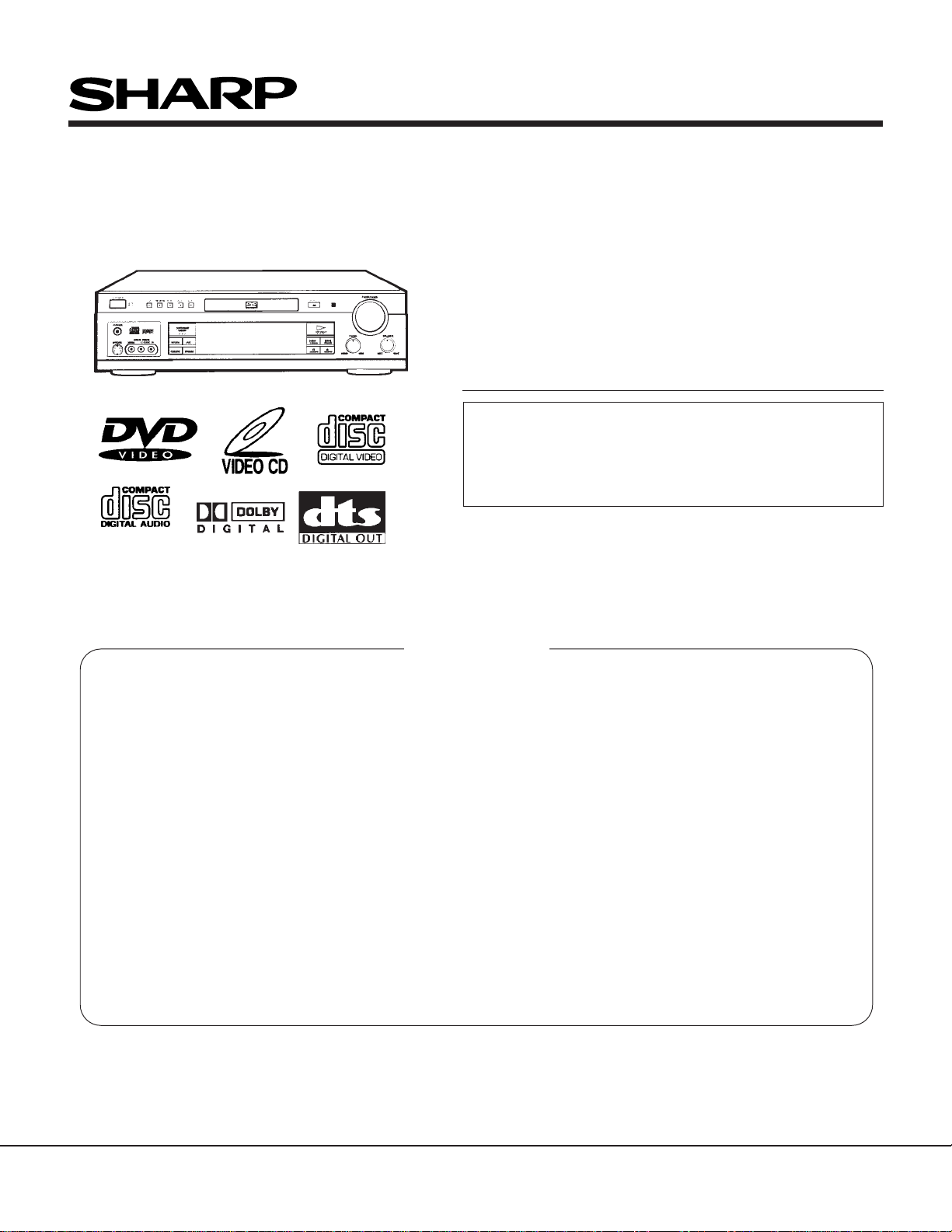
DV-A1000U
SERVICE MANUAL
S29C3DV-A1000
D VD VIDEO PLAYER
1. IMPORTANT SAFEGUARDS AND PRECAUTIONS ......................................................................1-1
2. FEATURES .....................................................................................................................................1-3
3. SPECIFICATIONS .......................................................................................................................... 3-1
MODEL DV-A1000U
4. PART NAMES ................................................................................................................................. 4-1
5. MAINTENANCE CHECK ITEMS AND EXECUTION TIME ............................................................ 5-1
6. DISASSEMBLY AND REPLACEMENT OF MAIN PARTS ............................................................. 6-1
7. EXPLANATION OF MECHANISM ..................................................................................................7-1
8. TEST MODE ................................................................................................................................... 8-1
9. TROUBLESHOOTING ....................................................................................................................9-1
10. IC FUNCTION LIST....................................................................................................................... 10-1
11.BLOCK DIAGRAM ......................................................................................................................... 11-1
12. WIRING DIAGRAM .......................................................................................................................12-1
13. SCHEMATIC DIAGRAMS .............................................................................................................13-1
14. PRINTED WIRING BOARD ASSEMBLIES ...................................................................................14-1
15.SEMICONDUCTOR LEAD IDENTIFICATION................................................................................15-1
16. REPLACEMENT PARTS LIST ......................................................................................................16-1
17. PACKING OF THE SET ................................................................................................................ 17-1
MODEL
In the interests of user-safety (Required by safety regulations in some countries) the set should be restored to its
original condition and only parts identical to those specified
be used.
CONTENTS
DV-A1000U
Page
SHARP CORPORATION
This document has been published to be used for
after sales service only.
The contents are subject to change without notice.
1
Page 2
DV-A1000U
SSVM
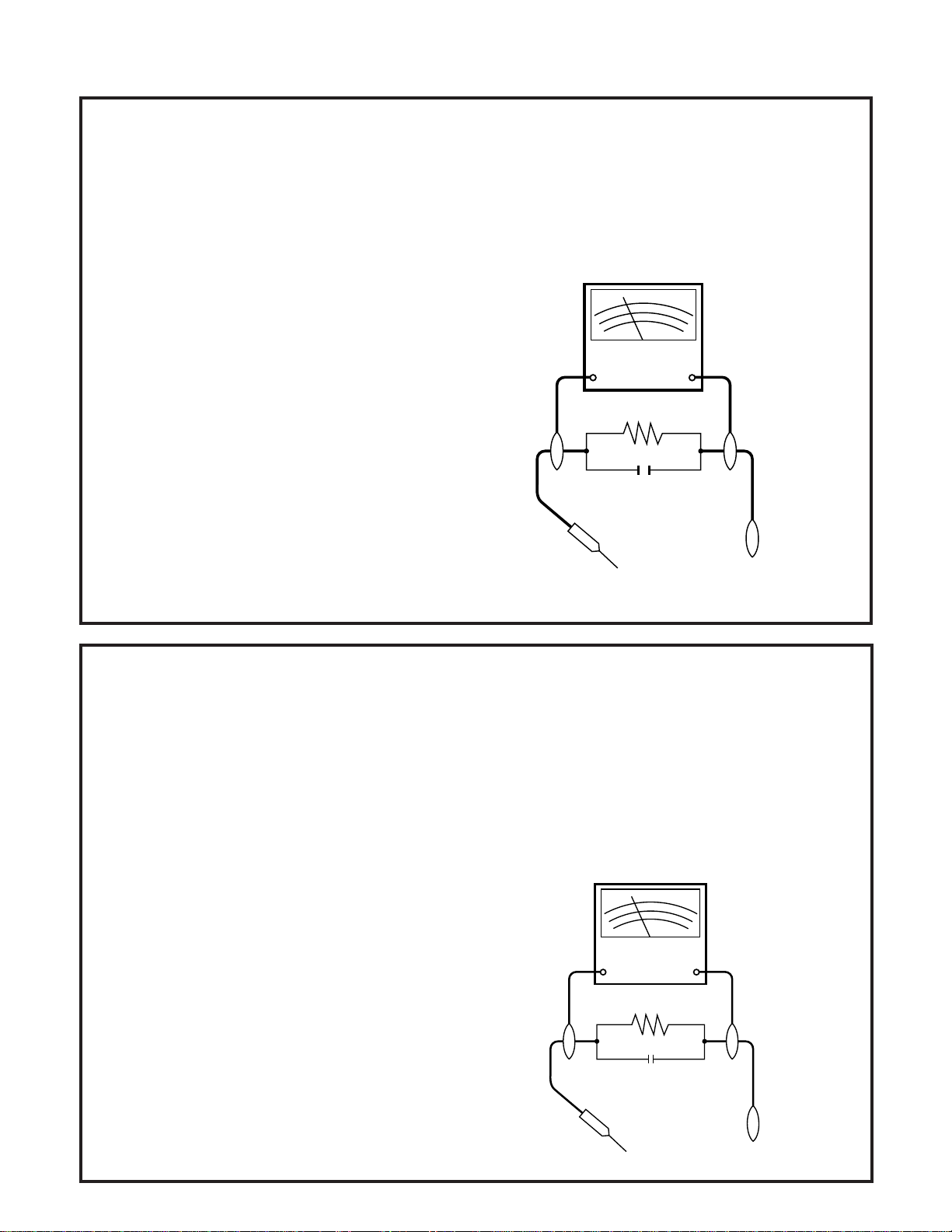
AC SCALE
1.5k ohms.
10W
CONNECT TO
KNOWN EARTH
GROUND
TO EXPOSED
METAL PARTS
0.15 µF
TEST PROBE
0.15 µF
SONDE D'ESSAI
VERS PIECES
METALLIQUES
EXPOSEES
VTVM
ECHELLE CA
1.5KOHMS
10W
CONNECTER A
UNE MASSE DE
TERRE CONNUE
1. IMPORTANT SAFEGUARDS AND PRECAUTIONS
1. IMPORTANT SERVICE NOTES
BEFORE RETURNING THE VIDEO CASSETTE
RECORDER
Before returning the video cassette recorder to the user,
perform the following safety checks.
1. Inspect all lead dress to make certain that leads are
not pinched or that hardware is not lodged between
the chassis and other metal parts in the video cassette
recorder.
2. Inspect all protective devices such as non-metallic
control knobs, insulation materials, cabinet backs,
adjustment and compartment covers or shields, isolation resistor/capacitor networks, mechanical insulators etc.
3. To be sure that no shock hazard exists, check for
current in the following manner.
● Plug the AC line cord directly into a 120 volt AC outlet
(Do not use an isolation transformer for this test).
● Using two clip leads, connect a 1.5k ohm, 10 watt
resistor paralleled by a 0.15µF capacitor in series with
all exposed metal cabinet parts and a known earth
ground, such as a water pipe or conduit.
● Use an SSVM or VOM with 1000 ohm per volt, or
higher, sensitivity or measure the AC voltage drop
across the resistor (See Diagram).
● Move the resistor connection to earth exposed metal
part having a return path to the chassis (antenna,
metal cabinet, screw heads, knobs and control shafts,
etc.) and measure the AC voltage drop across the
resistor. Reverse the AC plug on the set and repeat
AC voltage measurements for each exposed part.
Any reading of 0.45V rms (this corresponds to 0.3mA
rms AC.) or more is excessive and indicates a potential shock hazard which must be corrected before
returning the video cassette recorder to the owner.
1. NOTES DE SERVICE IMPORTANTES
AVANT DE RENDRE LE MAGNETOSCOPE
Avant de rendre le magnétoscope à l’utilisateur, effectuer
les vérifications de sécurité suivantes.
1. Vérifier toutes les gaines de fil pour être sûr que les fils
ne sont pas pincés ou que le matériel n’est pas coincé
entre le châssis et les autres pièces métalliques dans le
magnétoscope.
2. Vérifier tous les dispositifs de protection tels que les
boutons de commande non métalliques, les matériaux
d’isolement, le dos du coffret, les couvercles de
compartiment et ajustement ou les boucliers, les
réseaux de résistance / condensateur d’isolement, Ies
isolateurs mécaniques, etc.
3. Pour être sûr qu’il n’y a aucun risque de choc électrique,
vérifier le courant de fuite de la maniére suivante.
● Brancher le cordon d’alimentation secteur directement
dans une prise de courant de 120 volts. (Ne pas utiliser
de transformateur d’isolement pour cet essai).
● Utiliser deux fils à pinces et connecter une résistance
● Utiliser un VTVM ou VOM avec une sensibilité de 1000
● Déposer la connexion de la résistance à toutes les
de 10 watts 1,5 kohm en parallèle avec un condensateur
de 0,15 µF en série avec des pièces du coffret métallique
exposées et une masse de terre connue telle qu’un
tuyau ou un conduit d’eau.
ohms par volt ou plus ou mesurer la chute de tension
CA entre la résistance (voir diagramme).
pièces métalliques exposées ayant un parcours de
retour au châssis (connexions d’antenne, coffret
métallique, tétes de vis, boutons et arbres de commande,
etc.) et mesurer la chute de tension CA entre la résistance.
Inverser la fiche CA (une fiche intermédiaire non polarisée
doit être utilisée à seule fin de faire ces vérifications.) sur
l’appareil et répéter les mesures de tension CA pour
chaque piéce métallique exposée. Toute lecture de
0,45 V rms (ceci correspond à 0,3 mA rms CA) ou plus
est excessive et signale un danger de choc qui doit être
corrigé avant de rendre le magnétoscope à son
utilisateur.
2
1-1
Page 3
WARNING :TO REDUCE THE RISK OF FIRE OR ELECTRIC SHOCK, DO NO T EXPOSE
1.5A 250V
THIS APPLIANCE TO WET LOCATIONS.
CAUTION
RISK OF ELECTRIC SHOCK
DO NOT OPEN
CAUTION: TO REDUCE THE RISK OF ELECTRIC
SHOCK. DO NOT REMOVE COVER. NO
USER·SERVICEABLE PARTS INSIDE.
REFER SERVICING TO QUALIFIED SERVICE
PERSONNEL.
CAUTION
This symbol mark means following.
For continued protection against fire hazard, replace only with same type fuse
F9201 (5A, 125V) or F9101 (1.6A, 125V).
Camcorder
only
DV-A1000U
This symbol warns the user of uninsulated
voltage within the unit that can cause dangerous electric shocks.
This symbol alerts the user that there are
important operating and maintenance instructions in the literature accompanying this unit.
CAUTION
This symbol mark means following.
For continued protection against fire haz-
ard, replace only with same type fuse.
(F1; 1.5A 250V)
AC Adapter
only
ATTENTION:POUR REDUIRE LES RESQUES D'INCENDIE OU DE CHOC ELECTRIQUE,
NE PAS EXPOSER CET APPAREIL A LA PLUIE OU A L'HUMIDITE.
ATTENTION
RISQUE DE CHOC ELECTRIQUE
NE PAS OUVRIR
ATTENTION: AFIN DE REDUIRE LES RISQUES DE
CHOC ELECTRIQUE, NE PAS RETIRER LE
COUVERCLE, AUCUN ORGANE INTERNE
NE PEUT ETRE REPARE PAR
L'UTIUSATEUR, CONFIER L'APPAREIL A
UN DEPANNEUR QUALIFIE.
ATTENTION
Ce symbole signifie que l'on devra utiliser un fusible de même type (F9201
(5A, 125V) or F9101 (1.6A, 125V)) pour
assurer la sécurité.
Camcorder
seulement
Ce symbole signale à l'utilisateur la présence
d'une tension non isolée à l'intérieur de l'appareil
qui peut être la cause de secousses électriques
dangereuses.
Ce symbole avertit l'utilisateur que des instructions importantes relatives à l'utilisation
et àl'entretien se trouvent dans le manuel
accompagnant l'appareil.
ATTENTION
Ce symbole signifie que l'on devra uti-
liser un fusible de même type (F1; 1,5A,
250V) pour assurer la sécurité.
3
1-2
Adaptateur CA
seulement
1,5A 250V
Page 4
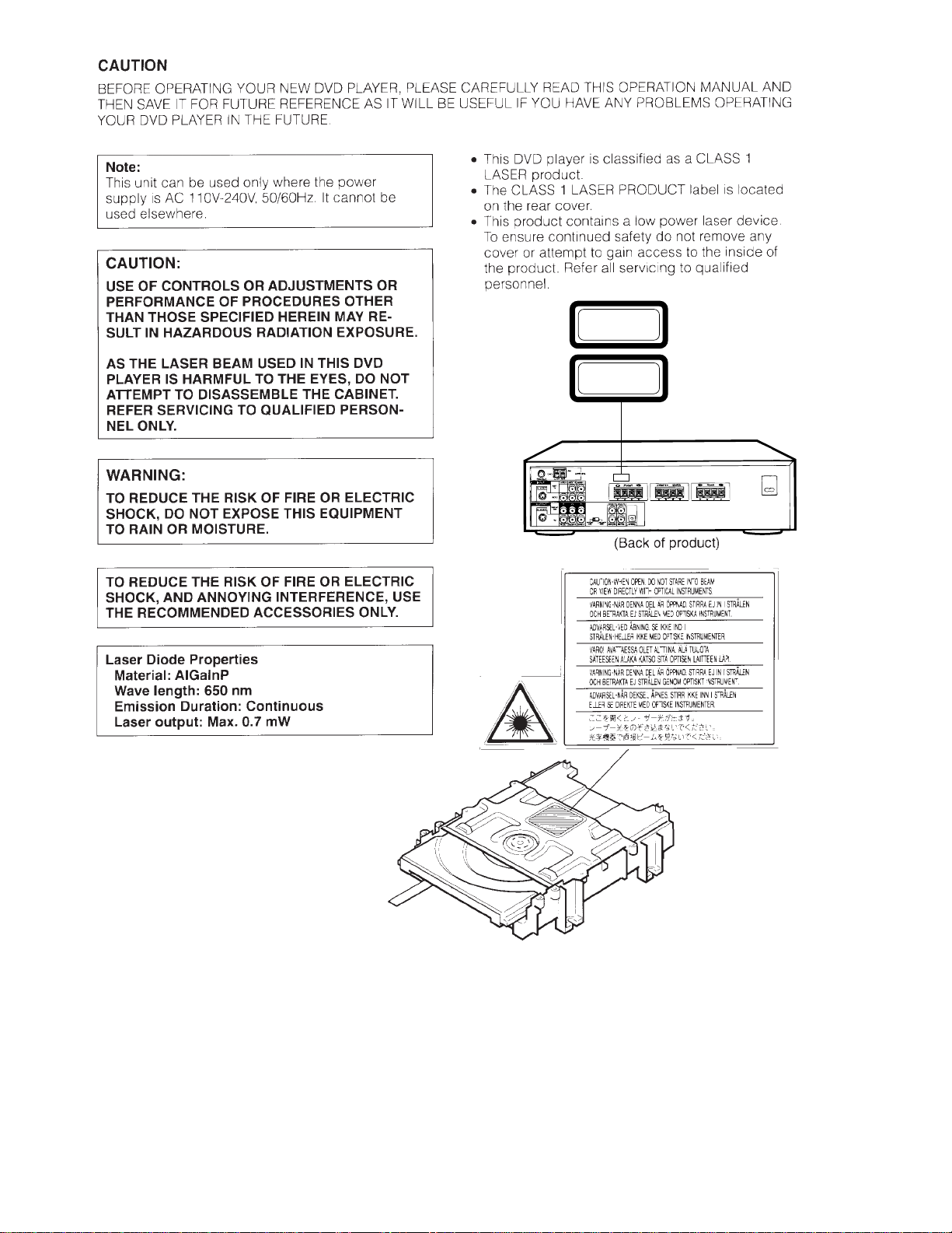
DV-A1000U
CLASS 1
LASER PRODUCT
PRODUCT LASER
DE CLASSE 1
2. FEATURES
• High-quality digital images
• High-quality digital sound
• Plays DVD, video CD and CD (Digital Audio) discs
• Built-in Dolby Digital decoder supporting Dolby Pro Logic*
2
digital output capability
• DTS*
• Separate color component output connectors (Y, P
• Built-in amplifier suports 6-channel Dolby Digital (AC-3) surround sound
• Built-in digital output connectors (optical/coaxial)
• Simulated surround sound
• Built-in AM/FM tuner
*1 Manufactured under license from Dolby Laboratories. "Dolby", "Pro Logic" and the double-D symbol are trademarks of Dolby Laboratories.
*2 "DTS" nad "DTS Digital Surround" are trademarks of Digital Theater Systems, Inc.
1
decoding and Virtual Surround
B and PR)
4
1-3
Page 5

3. SPECIFICATIONS
DVD Video Player
Signal System NTSC
Video signal Horizontal resolution: 500 lines
Audio signal 5.1ch output: Front L/R, surround L/R, center and subwoofer
Input/output jack
AUX (input) 1 AUDIO input jacks
AUX (input) 2 S-VIDEO input jacks/VIDEO and AUDIO input jacks
AUX (front panel input) 3 S-VIDEO input jacks/VIDEO and AUDIO input jacks
OUTPUT COMPONENT VIDEO output jack/S-VIDEO output jack/VIDEO•AUDIO output jack/AUDIO
Component color output Y output level: 1 Vp-p (75Ω)
S-video input/output Y input/output level: 1 Vp-p (75Ω)
Video input/output Input/output level: 1 Vp-p (75Ω)
Audio input Input level: 200 mV (47kΩ)
Audio output Output level: 200 mV (1kΩ)
Subwoofer audio output Max. Output level: 6 Vrms (1kΩ)
Digital audio I/F audio output Optical digital output: Optical jack
S/N ratio: more than 60 dB
Output jack: RCA Pin-jack
Output level: 2 Vrms (1kHz, 0 dB) (L/R)
Frequency characteristics:
For DVD linear PCM playback: 4 Hz to 22 kHz (48 kHz sampling)
CD playback:4 Hz to 20 kHz (EIAJ)
S/N ratio: CD: 96 dB (EIAJ)
Dynamic range DVD linear PCM: 96 dB (EIAJ)
CD: 96 dB (EIAJ)
Total harmonic distortion ratio CD: 0.006% (EIAJ)
Pickup:
Wave length: 650 nm
Laser output: Max. 0.7 mW
output jack/subwoofer audio output jack/digital audio output jack (coaxial/optical)
B output level: 0.648 Vp-p (75Ω)/100% Color
P
R output level: 0.648 Vp-p (75Ω)/100% Color
P
Output jack: RCA Pin-jack
C input/output level: 0.286 Vp-p (75Ω)
Input/output jack: S jack
Input/output jack: RCA Pin-jack
Output jack: RCA Pin-jack
Output jack: RCA Pin-jack
Output jack: RCA Pin-jack
Coaxial digital output: RCA Pin-jack
DV-A1000U
4 Hz to 44 kHz (96 kHz sampling)
Amplifier
Rated Output 6ch Power Amplifier
Front L/R 40W/40W (8Ω load, 60 Hz to 20 kHz), T.H.D 0.9%
Center 40W (8Ω load, 60 Hz to 20 kHz), T.H.D 0.9%
Surround L/R 40W/40W (8Ω load, 60 Hz to 20 kHz), T.H.D 0.9%
Subwoofer 40W (8Ω load, 20 Hz to 100 Hz), T.H.D 0.9%
Dynamic Power 45W x 2 channels (8Ω)
Speaker Output Speaker impedance: 8Ω
Tuner
Reception frequency bandwidths FM: 87.5 MHz to 108.0 MHz
AM: 530 kHz to 1710 kHz
Actual sensitivity FM: 14 dBµV
AM: 47 dBµV
S/N ratio FM stereo: 70 dB
FM mono: 75 dB
AM: 53 dB
Antenna FM: Coaxial, 75Ω
AM: Loop antenna
3-1
Page 6

DV-A1000U
Speaker
Front
Type: 2-way magnetically shielded speaker
16 cm (6.3*) woofer
5 cm (2.0*) tweeter
Size 210 mm (8.3*) x 330 mm (13.0*) x 218 mm (8.9*) (W x H x D)
Mass: 3.7 kg (8.2 lbs)
Impedance: 8Ω
Rated input: 40W
Max. permissible input: 80W
Center
Type: 2-way magnetically shielded speaker
13 cm (5.1*) woofer
5 cm (2.0*) tweeter
Size: 400 mm (15.7*) x 165 mm (6.5*) x 163 mm (6.4*) (W x H x D)
Mass: 2.9 kg (6.4 lbs)
Impedance: 8Ω
Rated input: 40W
Max. permissible input: 80W
Rear
Type: 2-way
13 cm (5.1*) woofer
5 cm (2.0*) tweeter
Size: 210 mm (8.3*) x 165 mm (6.5*) x 163 mm (6.4*) (W x H x D)
Mass: 1.6 kg (11.5 lbs)
Impedance: 8Ω
Rated input 40W
Max. permissible: 80W
Sub-woofer
Type: Full range magnetically shielded speaker
16 cm (6.3*) super-woofer
Size: 210 mm (8.3*) x 330 mm (13.0*) x 340 mm (13.4*) (W x H x D)
Mass: 5.2 kg (11.5 lbs)
Imdependence: 8Ω
Rated input: 40W
Max. permissible: 80W
Common Specifications
Specifications are subject to change without notice.
Weight and dimensions are approximate.
Digital Output
· The digital output format (optical or coaxial) used in this DVD player is linear PCM audio sampling at 44.1 kHz or 48 kHz.
Linear PCM sound for DVD video discs sampled at 96 kHz cannot be output digitally.
Check the disc jacket for information on the audio sampling used.
Headphone Max. Output level: 52mW (32Ω)
Output jack: Stereo standard jack
Power supply 120 V AC, 60 Hz
Power consumption 150W (0 W when switched off)
Dimensions 430 mm (16.9*) x 130 mm (5.1*) x 402 mm (15.4*) (W x H x D)
(including attachments)
Weight 9.3 kg (20.5 lbs)
Operating temperature 5°C to 35°C (41°F to 104°F)
Storage temperature -20°C to 55°C (-4°F to 131°F)
3-1. ACCESSORIES
Accessories: S-video cable x 1, Video/audio cable x 1, AC power cord x 1, UM3 battery x 2,
Remote Control Unit x 1, AM loop antenna x 1, Simple FM antenna x 1, FM antenna adaptor x 1,
Speaker cables [2.5 m (8.2 ft)] x 4, Speaker cables [10 m (32.8ft)] x 2, Speakers
3-2
Page 7
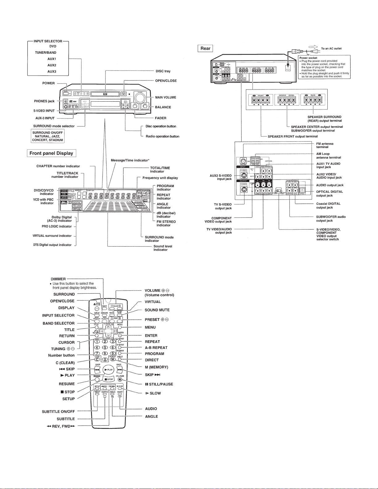
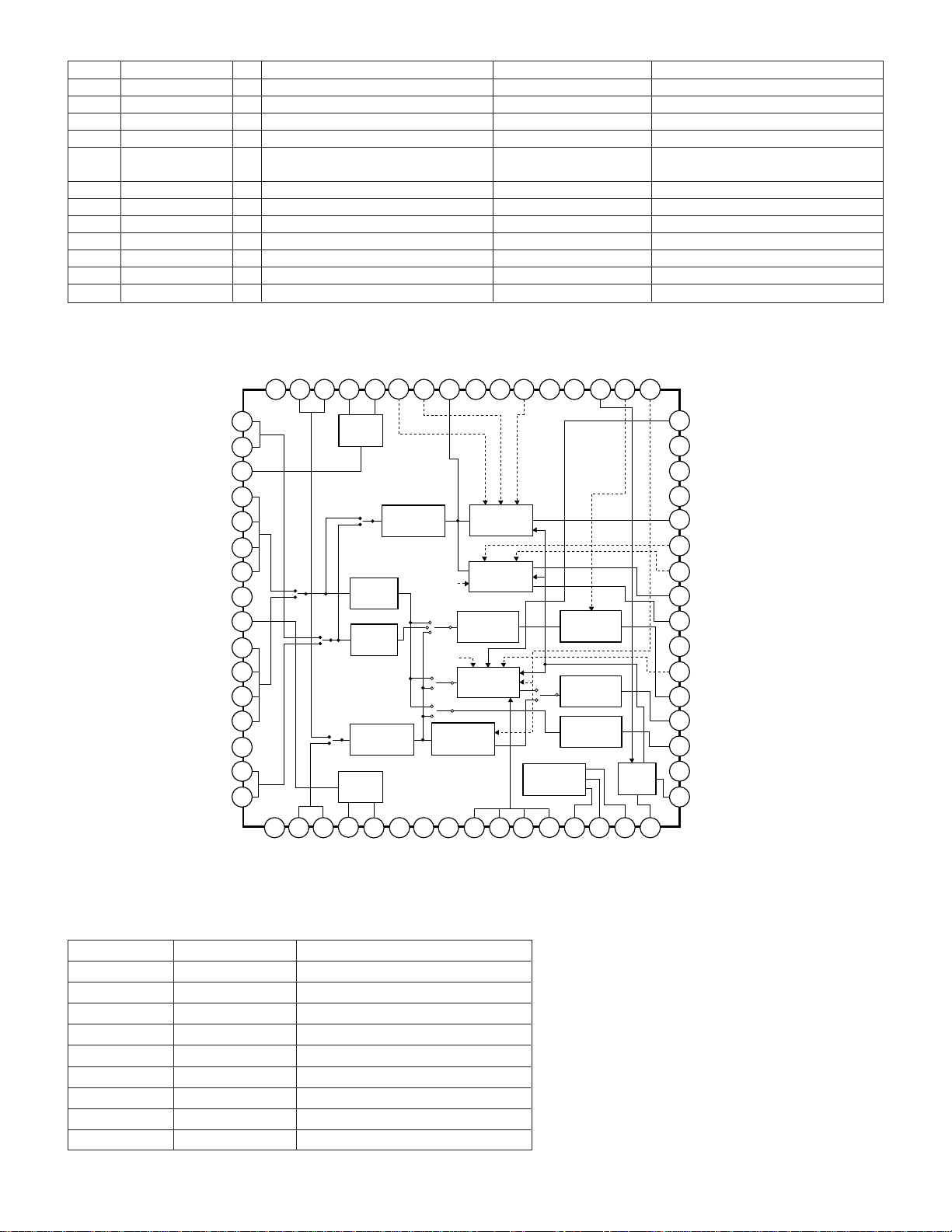
4. PARTS NAME
DV-A1000U
4-1
Page 8
DV-A1000U
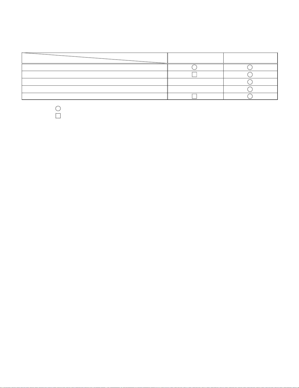
5. MAINTENANCE CHECK ITEMS AND EXECUTION TIME
MECHANICAL PARTS REGUIRING PERIODICAL INSPECTION
Use the following table as a guide to maintain the mechanical parts in good operating condition.
Parts
Pickup
Spindle Unit
Sled Motor
Loading Motor
Belt
Note : Part Replacement
: Cleaning
(For cleaning, use a lint-free cloth danpened with pure isopropyl alcohol.)
Maintained
1,000 hrs.
2,000 hrs.
CARES WHEN USING THE PICKUP
1. The laser light having wavelength 650 nm is emitted from the objective lens. BE CAREFUL SO THAT THE LASER
LIGHT DOES NOT ENTER DIRECTLY INTO YOUR EYE.
2. The semiconductor laser may be easily damaged by electrostatic charges. When handling the pickup, take care so that
the electrostatic charge is not generated.
3. The semiconductor laser may be easily damaged by overcurrent. Use the power supply unit which does not give any
spike current when the power is turned on and off.
4. Carefully remove the dust and dirt from the objective lens with the lens blower.
When handling the objective lens, take due care so that it is not contaminated with fingerprint, etc. If the objective lens
is contaminated, impregnate the cleaning paper with a small quantity of solvent (isopropyl alcohol), and gently wipe to
clean.
5. The ozone layer depleting components (ODC) are not used in the production process for the product.
5-1
Page 9
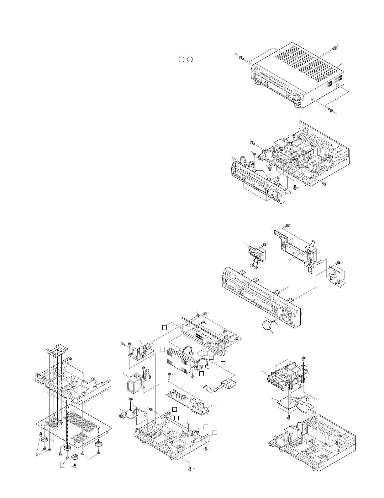
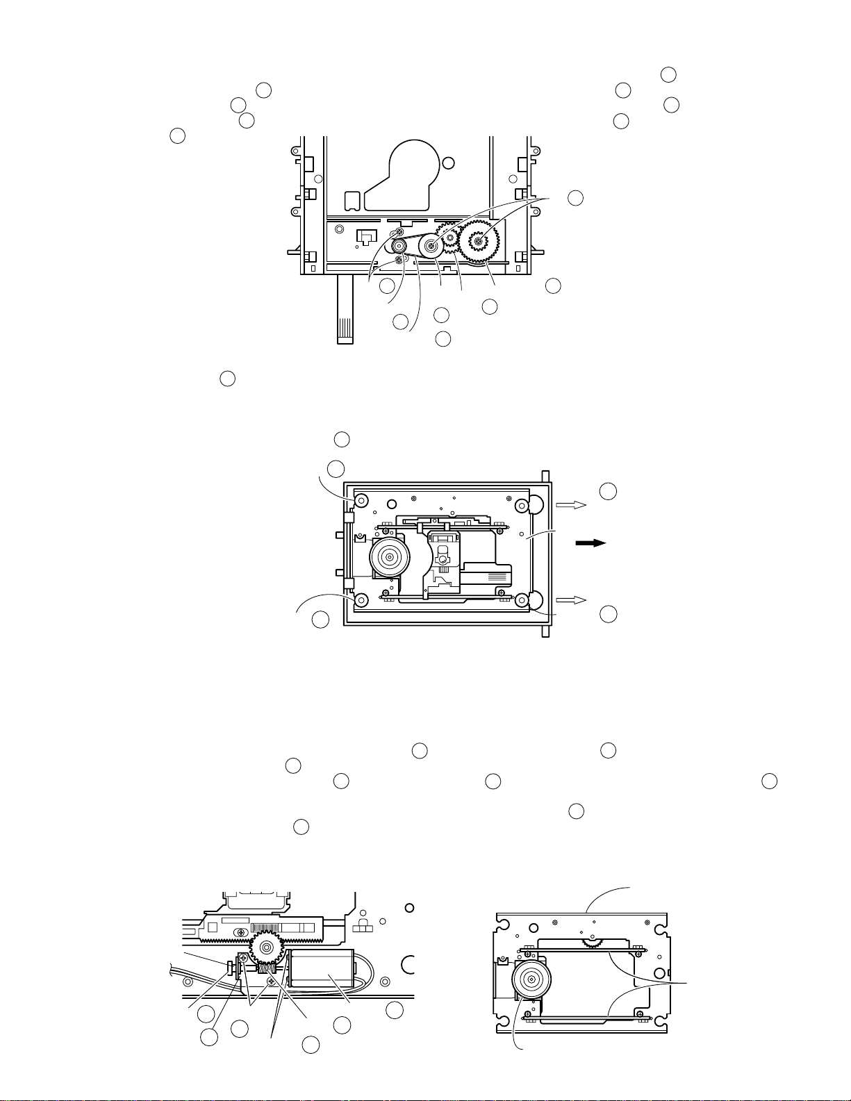
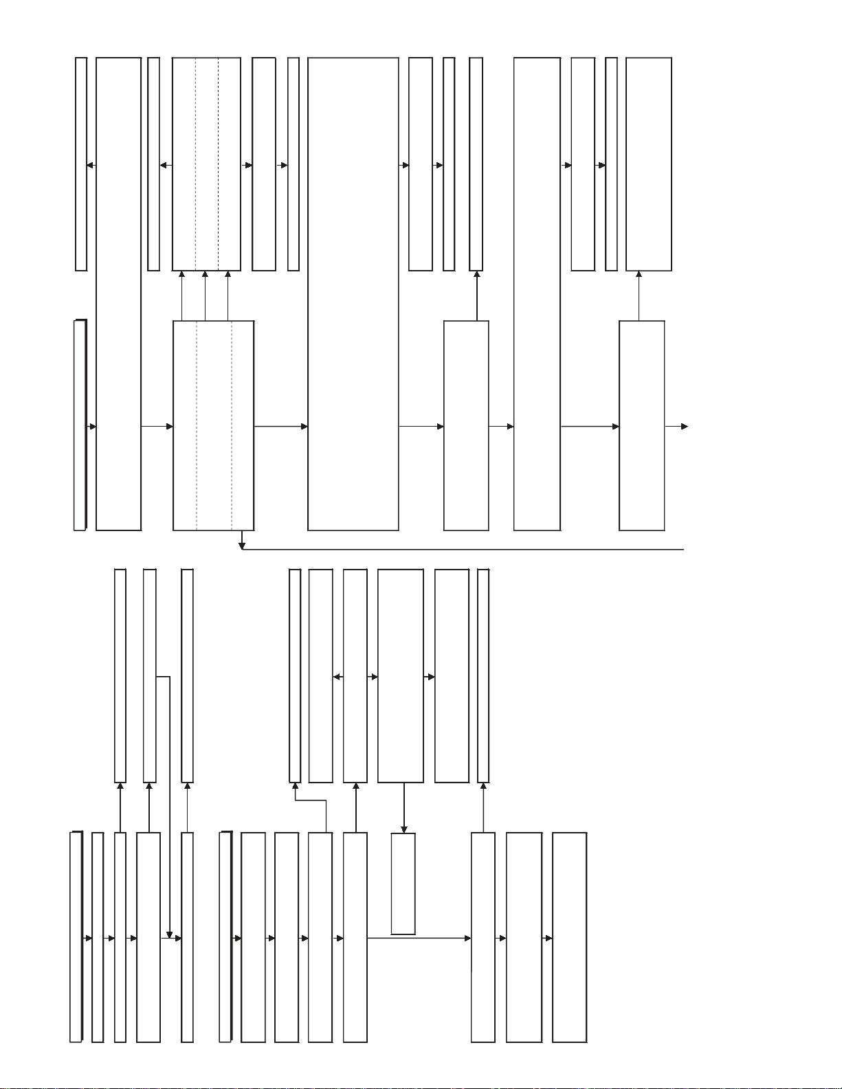
6. DISASSEMBLY AND REPLACEMENT OF MAIN PARTS
6-1. DISASSEMBLY
1. Remove five screws (A), and remove the cabinet.
Note: When assembling it, tighten the screws in order of 1 - 2 .
(Because the set may rise a little by tightening the screws.)
[Figure 1.]
2. Remove the two screws (B) at the lower side of front panel.
3. Remove the two screws (C) of side.
4. Remove the two screws (D) fixing the font panel to the mechanism.
5. Remove both side pawls and lower pawl. [Figure 2.]
6. Remove the PWB fitted to the front panel.
(Front AV PWB (E), 4 pcs., indication display PWB (F), 7 pcs., volume
PWB (G), 3 pcs.)
7. Withdraw the master volume, and remove the VR nut and washer.
[Figure 3.] (At this time the tray decoration plate can be removed.)
8. Remove the four screws (H) for fitting the mechanism unit.
9. Remove the three screws (J) at the lower side of mechanism unit.
(Main PWB) [Figure 4.]
10. Remove the two screws (K) for fitting the headphone PWB.
11. Remove the four screws (L) fitting the transformer.
12. Remove one screw (M) fixing the power PWB, remove the two screws
(N) of AC inlet, remove the screw (P) fixing the transistor, and remove
the spacer hook.
13. Remove the three screws (Q) fixing the FM tuner.
14. Remove the two screws (R) of bottom plate which fix the radiation
plate.Remove the two screws (S).Remove the nine screws(T). Shift the
radiation plate and PWB to this side, remove the terminal from the
terminal block, and lift.
15. Remove the five screws (U) of PWB. Remove the two screws (V) fixing
the terminal PWB.
16. Remove the two screws (W) and three screws (X) fixing the terminal
block. [Figure 5.]
(A) x2 ①
(C)
(D)
Pawl x2
Operate PWB
Front AV PWB
(D)
Pawl
Front Panel
(E) x4
Figure 1
Pawl x2
Figure 2
(F) x7
(B)
DV-A1000U
(A) ②
Top Cabinet
(A) x2 ①
(C)
(G) x3
Volume PWB
17. Remove the sixteen screws (Y). [Figure 6.]
Power PWB
(M)
(P)
Power Transformer
(K) x4
Headphone
PWB
(Y) x8
(Y) x4
(Y) x4
(L) x4
(S)
(N) x2
G
D
(V) x2
G
D
D
Figure 5Figure 6
D
(S)
(R) x2
(W) x2
(T) x6
(U) x2
J
G
J
Terminal PWB
E
G
(X) x3
(Q) x3
Terminal Plate
E
FM Tuner
VR Nut
(T) x3
(U) x3
Mechanism Unit
Washer
Master Volume
Figure 3
(H) x4
Main PWB
(J) x3
Figure 4
6-1
Page 10
DV-A1000U
VIDEO
Tray Decoration Panel
6-2. REPLACEMENT OF MAIN PARTS
<Disassembling and assembling procedure>
· Removing the tray (emergency ejection)
Removing the tray lock (set state)
Insert a thin plate into the hatching part, slowly move the it in the arrow direction so that the tray is moved out a little in the arrow direction.
Note: In this state the tray cannot be removed completely.
Tray Decoration Panel
· Drive Unit State
VIDEO
Slowly move in the arrow direction, using the screwdriver having a fine head.
<Disassembling and assembling the mechanism chassis>
1. Remove the pickup FPC and loading relay FFC A from the main PWB.
Note: Fit the conductive rubber cap to the front end of pickup FPC (short-circuit).
2. Remove the solder joint of loading relay PWB at drive unit rear side.
1 Sled motor lead wire (Yellow·Orange)
2 IN SW lead wire 2 (White)
3
3 Spindle motor lead wire (Red·Black)
4 Loading motor lead wire (Red·Black)
5 Remove each lead wire from the claw.
2
3
3. Remove the relay PWB mounting screw B
(M2.6S + 6S S tight), and remove the relay PWB C .
Brack
4
L motor2
Red
Lmotor2
1
Orange
Yellow
Brown
Brown
Brack
Red
SL motor1
SL motor2
SW
GND
SP1
SP2
Remove the lead wire
A
1
2
B
C
4
4. Disassembling the mechanism chassis moving chassis assembly
(1) Remove the four M2.6 screws A , and remove the clamped top plate B .
B
A
A
P tight screw
with M2.6 washer
A
B
(2) Remove the M2.6 screw C .
(3) Holding aslant upward the mechanism chassis moving chassis assembly D in the arrow direction, remove.
Note: The slide rack E must be moved to the left side as shown in diagram.
Take care so that the lead wires, especially the earth sponge G at the pickup FPC F front end, must not beremoved.
P tight screw with
M2.6 washer
C
F
G
Mechanism chassis moving
chassis assembly
D
Slide rack
E
A
P tight screw
with M2.6 washer
6-2
Page 11
5. Disassembling the loading drive system
Insulator
Insulator
Insulator
Insulator
Mechanism chassis
C
B
B
C
[Item 3 of previous page] Remove the L. relay PWB. (Otherwise the L motor cannot be removed in step 6 .)
(1) Remove the two M2 screws A . (4) Remove relay gear 2 E .
(2) Remove the tray pinion B . (5) Remove the two M1.7 screws F .
(3) Remove the relay gear 1 C together with the (6) Remove the L motor G (with pulley) downward.
timing belt S D .
M2
A
DV-A1000U
F
M1.7
L.Motor Pully
L.Motor
Timing Belt
Relay
gear2
Tray pininon
E
Relay
gear1
C
G
D
B
6. Disassembling the mechanism chassis from the moving chassis
(1) Remove the insulator B (2 pcs. at the right side in diagram) parallel in the arrow direction.
(At this time it is better to insert the fine head of screw driver at the ID side of insulator and to move in the arrow direction, which
facilitates removal.)
(2) Remove the mechanism chassis in the arrow direction, pulling upward aslant.
At this time take care so that the insulator C (left side, 2 pcs.) is not damaged. (Do not put at once the mechanism chassis
assembly.)
7. Replacing the pickup
After replacement the tilt adjustment with the aid of jitter meter and other special equipment is required. Therefore, it is impossible
to replace on site. (The same as item 9 of next page). Replace as service chassis.
8. Replacing the Sled Motor
(1) At the rear side of chassis remove the two M1.7 screws A , and remove the motor angle B .
(2) Remove the thrust holding screw C (for easier removing wipe off the thread lock).
(3) Remove the two motor fitting screws M1.4 D , and replace the motor E . Motor is replaced in the state while the worm F is
kept press-fitted to the output shaft.
Note: When installing the motor, take care so that the worm does not damage the ANG B hole.
(4) Screw in the thurust holding screw C , adjust the worm front end clearance to 0 to 0.1 mm, and apply screw lock.
9. Replacing the spindlw motor
Since the pickup optical axis and turntable inclination of DVD are adjusted with higher accuracy than of CD/MD, make a replacement
as a mechanism service chassis ass'y (refer to Parts List).
Mechanism chassis
Apply screw-lock
M1.7 Screw
Thurust holding screw
Motor Angle
C
A
B
M1.4 Screw
Worm
D
Sled motor
F
Guide shaft
E
Spindle motor unit
6-3
Page 12
DV-A1000U
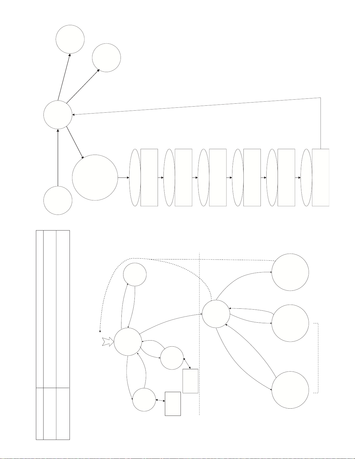
7. EXPLANATION OF MECHANISM
(1)Tray loading mechanism
When the tray loading motor rotates clockwise, motion is transmitted to the slide rack D through the intermediate gear 1
A , intermediate gear 2 B and tray pinion C , resulting in insignificant motion in the arrow direction.
The slide rack is linked with the operating chassis. It lowers the pickup mechanism.
The protrusion of slide rack E is linked with the tray through the groove at the rear side of tray, so that the tray is
pushed ahead a little. When the tray is pushed out, the slide rack is disconnected from the tray pinion, and at the same
time the gear at the rear side of tray is connected with the tray pinion, and the tray is pushed ahead.
When the tray is pushed out fully, the slide rack moves further in the arrow direction through the groove at the rear side
of tray. The tray position detection switch F is turned on, and the tray loading motor stops.
When the tray closes the operation is as follows. If the tray OPEN/CLOSE button or tray is pressed and the detection
switch is turned off, the tray loading motor rotates counterclockwise, so that the tray is retracted. When the detection
switch is turned on again, the tray loading motor stops.
This groove is linked with trhe pawl of
pickup mechanism
Tray position detection switch
Slide rack
F
D
Pawl kinled with the groove at the
rear side of tray
E
Intermediate gear 2
Tray pinion
Intermediate gear 1
C
(2)Pickup feed mechanism
When the sled motor A rotates, the rack C moves through the sled pinion B so that the pickup D is moved to the
internal or external periphery.
When it is moved to the innermost periphery, the position detection switch E is pushed by the rack, so that the position
of pickup is initialized.
(3)Disc rotation mechanism
Pickup
Position detection
switch
E
Spindle motor
The spindle motor is used to rotate.
IC701 is used to control.
When the spindle motor is replaced, replace the
spindle unit.
Rack
C
B
A
Sled pinion
7-1
B
Pickup
Sled motor
D
A
Page 13
DV-A1000U
Test Mode Operation
SystemOpe( )
DVDOpe( )
Systest( )
DVD Disc detection
CD Disc
detection
No Disc and
Test 0 (F0h) key
Eject or
error
Eject or
error
Power
Off
Power
Off
Memory Test
Model number
Program version
Region code
microcode version
Dynamic
Test
Tray Open/Close
Sled Move
DVD Servo
CD Servo
Video Test
Initial Screen
Test Pattern
'1' Key
'2' Key
'3' Key
FlashOpe( )
Reset
Start
Flash rewriting key
Static Test
Test0
(F0h)
key
Branching with
ten keys
Test0
Key
Test0
Key
Test0
(F0h)
key
OSD
Adjustment
value display
OSD
Adjustment
value display
Initial resetting
CDOpe( )
Note: For test mode input,
"F0h" = PLAY + Stop
The keys of main body are doubly pressed.
Systest( )
(0xF100)
Dinamic
Test
Video
Test
'1' Key
'2' Key
'3' Key
Transition of test mode status (1)
Memory Test
Last Update display
ErrDisplay0 ErrDisplay1
10000000 ********
(last update)
(last update)
Play Key
System( )
Test0 Key
SystemMode
=
0xF100-0xF1FF
Memory Test
Model number
Program version
Region code
microcode version
Model Number display
(Model Number)
Play Key
Region code display
(Region code)
Play Key
Microcode version
display
(Microcode. Ver)
Play Key
Program Version display
(Program version)
Play Key
Servo version display
(Servo. Ver)
Play Key
ErrDisplay0 ErrDisplay1
10000001 ********
ErrDisplay0 ErrDisplay1
10000002 ********
ErrDisplay0 ErrDisplay1
10000004 ********
ErrDisplay0 ErrDisplay1
10000005 ********
ErrDisplay0 ErrDisplay1
10000003 ********
Memory Test Mode Program version indicaiton.
Video Test Mode Ordinary test pattern indication, and copy guard signal added test
8. TEST MODE
pattern indication are given.
continuous playback, jump test are performed.
Mecha Test Mode Servo system initialization, tray opening and closing, laser, servo,
EXPLANATION OF OPERATION AT THE SYSTEM START
8-1.
8-1
Page 14
DV-A1000U
SysTest( )
(0xF100)
Memory
Test
Dinamic
Test
'1' Key
'2' Key
'3' Key
System( )
Test0 Key
Video
Test
SystemMode
=
0xF201-0xF204
(1)Test pattern display
20000001 00000000
(2)Copy guard (AGC alone)
20000002 00000000
Play
key
Play
key
Play
key
Play
key
Test0
Key
(3)Copy guard
(AGC + Color stripe 1)
20000003 00000000
(4)Copy guard
(AGC + Color stripe 2)
20000003 00000000
Transition of test mode status (2)
Video Test
In Video Test mode, the color bar test pattern
is first displayed and output, and the display
data mode is changed every entry of PLAY key
as shown in the right. Here, it returns to Sys
Test ( ) if any Test 0 (F0h) key is input in the
test display.
Transition of test mode status (3)
Dinamic Test
Systest( )
(0xF100)
Memory
Test
Dynamic
Test
'1' Key
'2' Key '3' Key
System( )
Test0 Key
Video
Test
SystemMode
=
0xFC00-0xFDFF
Servo Initialize
ErrDisplay0 ErrDisplay1
30000000 00000000
ErrDisplay0 ErrDisplay1
3000E000 EEEEEEEE
(Servo Initial Err)
Tray Eject
ErrDisplay0 ErrDisplay1
30000001 00000000
ErrDisplay0 ErrDisplay1
3000E001 EEEEEEEE
(Tray Eject Err)
Open/Close Key
or hand-push Wait
Tray Load
ErrDisplay0 ErrDisplay1
30000002 00000000
ErrDisplay0 ErrDisplay1
3000E002 EEEEEEEE
(Tray Load Err)
Test0 Key
Wait
SRV Play Test ( )
Continuous replay jump
test mode
'1' or '2'or'3'
Key Wait
SRV Step Test ( )
Step execution mode
Laser Test ( )
Laser Test mode
'1'
'2'
'3'
'1'
Key Wait
Refer to the step
test mode.
Refer to the jump
test mode.
ErrDisplay0 ErrDisplay1
DD000100 00000000
ErrDisplay0 ErrDisplay1
DD000200 00000000
ErrDisplay0 ErrDisplay1
DD000300 00000000
Every input of "1" key, LDON &
the sled moves outward, and the
spindle motor moves also insignificantly.
Note: Tray Err is not
retried in the mode.
8-2
Page 15
DV-A1000U
SRV Step Test( )
SRV Step Test( )
Step Test Mode
ex. DVD mode
ErrDisplay0 ErrDisplay1
DD000200 00000000
ErrDisplay0 ErrDisplay1
DD000204 7 000000
ErrDisplay0 ErrDisplay1
DD000205 9
11
0000
ErrDisplay0 ErrDisplay1
DD000206
7 4 5 00(CD)
8 5
0000(DVD)
AdjDisplay( )
(0xFF00)
'PLAY'
'STILL'
'PLAY'
'PLAY'
'STILL'
'STILL'
'PLAY'
DDT step 1 operation
ErrDisplay0 ErrDisplay1
DD000201 2 3 4 00
ErrDisplay0 ErrDisplay1
DD00E201 2 3 4 EE
'PLAY' or 'STILL'
'STILL'
ErrDisplay0 ErrDisplay1
DD000202 3 6 0000
'PLAY'
'STILL'
ErrDisplay0 ErrDisplay1
DD000203 4 6
11
00
'PLAY'
'STILL'
DDT step 1 operation
Executed till focus of DDT is turned on.
The numerals shown on Err Display 1
indicate the following adjustment values.
DDT step 2 operation
Track balance adjustment and track
thread on are executed.
DDT step 3 operation
After RF gain is adjusted for a certain
time, the just focus is adjusted.
After end, RF gain adjustment is started
again.
DDT step 4 operation
Focus gain is adjusted.
DDT step 5 operation
Track gain is adjusted.
DDT step 6 operation
On the 2-layer disc, the just focus
adjustment and focus gain adjustment
of layer 1 are done.
On CD, interrupt of SUB-Q is allowed,
TOC is read/set, and mute is turned off.
(for error)
(for error)
(for error)
(for error)
(for error)
(for error)
ErrDisplay0 ErrDisplay1
DD00E202 3 6 00EE
ErrDisplay0 ErrDisplay1
DD00E203 4 6
11
EE
ErrDisplay0 ErrDisplay1
DD00E204 7 0000EE
ErrDisplay0 ErrDisplay1
DD00E205 9
11
00EE
ErrDisplay0 ErrDisplay1
DD00E206
7 4 5
EE(CD)
8 5
00EE(DVD)
DDT step 2 operation
DDT step 3 operation
DDT step 4 operation
DDT step 5 operation
DDT step 6 operation
'PLAY' or 'STILL'
'PLAY' or 'STILL'
'PLAY' or 'STILL'
'PLAY' or 'STILL'
'PLAY' or 'STILL'
Servo adjustment value
Reading-out mode
SRVPlayTest( )
Continuous replay & jump mode
ErrDisplay0 ErrDisplay1
DD000300 ********
SRV Play Test( )
In the continuous replay mode, the current sector
address is displayed on ErrDisplay 1.
Key Wait
TR Jump command publication
In SRV Play Test ( ), key is input and number of TR jumps is specified as follows.
[Next replay] = Layer Jump
* Here, key allocation may be changed.
* Layer jump operation is not guaranteed except during 2-layer DVD test.
Key Name
[1]
[4]
[7]
[Clear]
[2]
[5]
[8]
[Skip(-)]
(Code)
01h
04h
07h
1Fh
02h
05h
08h
2Dh
Jump Number of TRs
-1
-102
-510
-511
-765
-766
-7000
-15000
Key Name
[3]
[6]
[9]
[Memory]
[Repeat]
[A-B]
[Program]
[Skip(+)]
(Code)
02h
06h
09h
1Ch
35h
36h
1Eh
2Eh
Jump Number of TRs
+1
+102
+510
+511
+765
+766
+7000
+15000
2 ........... Focus Offset
3 ........... Track Offset
4 ........... 0-Layer Focus Balance
5 ........... 1-Layer Focus Balance
.............. In case of CD, focus balance after correction.
6 ........... Track Balance
7 ........... 0-Layer Focus Gain
........... RF Gain
8 ........... 1-Layer Focus Gain
9 ........... Track Gain
11
8-3
Page 16
DV-A1000U
DVDOpe( )
(0x4000)
CDOpe( )
(0x1000)
AdjDisplay(*)
(0xFF00)
Test1
(F1h)
key
Test1
(F1h)
key
During stop in DVD/CD/VCD mode,
servo adjustment value reading-out
mode is selected if Test 1 key (F1h)
is input.
(1)Servo version display
F1000001 ********
'PLAY'
In the servo adjustment value reading-out mode,
the focus offset value is first displayed. Every input
of PLAY key, the displayed data is changed as
shown in the left.
After the servo step test, the internal circumference
SW value (ID) display is not defined.
SRV Step Test( )
After measurement is ended in the servo
step test mode,the servo adjustment value
reading-out mode is selected.
'PLAY'
'PLAY'
'PLAY'
'PLAY'
'PLAY'
'PLAY'
'PLAY'
'PLAY'
'PLAY'
If the servo adjustment value reading-out
mode is selected, disc is stopped.
'PLAY'
Argument of AdjDisplay(*)
is char 0:CD/1:DVD.
'PLAY'
(2)Focus offset value display
F1000002 ********
(3)Track offset value display
F1000003 ********
(4)0-layer focus balance value display
F1000004 ********
(5)1-layer focus balance value display
F1000005 ********
(6)Track balance value display
F1000006 ********
(7)0-layer focus gain value display
F1000007 ********
(8)1-layer focus gain value display
F1000008 ********
(9)Track gain value
F1000009 ********
(10)RF amplitude value display
F100000A ********
(11)RF gain value display
F100000B ********
(12)Internal circumference switch ID
value display
F100000C ********
Servo adjustment value
reading-out mode
22 23 24 25 26
9 10111213141516
(In case of CD, 0-Layer focus balance after correction.)
17 18 19 20 21
12345678
(2) 3, 4 .................. 1-layer focus gain
(3) 5, 6 .................. 0-layer focus balance
OSD adjustment value display
1. Press "FOh" key during disc replay. (Multiple press of S. PICTURE and STOP)
2. The following screen is displayed on OSD.
3. OSD display is turned off with "FOh" key.
(1) 1, 2 .................. 0-layer focus gain
(4) 7, 8 .................. 1-layer focus balance
(5) 9, 10 ................ Track offset
(6) 11, 12 .............. Track gain
(7) 13, 14 .............. Track balance
(8) 15, 16 .............. RF gain
Hexadecimal data from (1) to (8).
8-4
Page 17
DV-A1000U
Power cannot be supplied.
Check the power transformer primary side circuit.
(T9301,SW9202,AC9201,CN9202,ACCord,etc.)
Yes
Yes
Is fuse (F9201) normal?
Check the audio output power circuit +30.8V,
-30.8V line. (D9201,C9201,C9203,etc.)
Remove the connector CN9203, replace the
fuse (F9201), and turn on power again. Does
fuse (F9201) blow at this time?
The fuse (F9101) is cut.
Check whether there is leaking or short-circuited
part at primary side.(L9103,VR9101,Q9102,Q9104,
D9114,D9115,etc.) If any defect is found in Q9102,
Q9104, D9114 or D9115, replace them at the same
time.
When the output voltage fluctuates.
No
Does the secondary side photocoupler circuit
operate normally?
Check the circuit, and replace part.
(D9115,D9111,D9106-8,Q9101,Q9103,etc.)
Yes
Yes
Replace D9115.
When buzz is heard in the vicinity of power circuit.
(1)
Check for short-circuiting of rectifying diode and circuit in secondary side rectifying circuit.
(D9102-5,D9116,IC9001-2,IC9004,etc.)
(2)Check the audio output power circuit +30.8V, -30.8V line.(D9201,C9201,C9203,etc.)
(3)Check the AV power circuit +12V, -12V line.(D9401,IC9401-2,C9401-9,etc.)
Yes
Remove the connector CN9401, replace the
fuse (F9201), and turn on power again. Does
fuse (F9201) blow at this time?
Check for short-circuiting of rectifying diode and
circuit in secondary side rectifying circuit.
(D9102-5,D9116,etc.)
No
Does the Firstary side photocoupler circuit
operate normally?
Check the circuit, and replace part.
(D9115,D9112-3,etc.)
The power +30.8V, -30.8V for audio output is not
output.NoReplace D9201.
Yes
Is the rectifying diode D9201 normal?
Check the connector CN9203 and power
transformer T9301.
No
No
Is fuse (F9101) normal?
Refer to the flow chart No.2.
Yes
No
Is AT5.3V line voltage normal?
Check whether there is leaking or short-circuited
part in the primary circuit. (Q9102, Q9104, D9114,
D9115, etc.). If any defect is found in Q9102, Q9104,
D9114 or D9115, replace them at the same time.
Yes
Is filament voltage normal (AT 10.5V, AT 7.5,
AT -35V)?
No
Check the rectifying circuit of secondary circuit.
Unplug the power cord, and after several seconds
plug in again. Is normal state recovered at this time?
Yes
No
Check the AV power circuit +12V, -12V line.
(D9401,IC9401-2,C9401-9,etc.)
FLOW CHART NO.1
FLOW CHART NO.2
FLOW CHART NO.3
FLOW CHART NO.4
FLOW CHART NO.5
The fluorescent indicating tube does not light.
No
Is 5V supplied to the pins 16 and 74 of IC5001? Check the D 5V line.
Yes
No
Is approx. 5V applied to the pin 10 of IC5001? Check the RESET(L) line and IC509, IC512.
Yes
No
Is 4.0 MHz oscillation signal observed on the pins
14 and 15 of IC5002?
Check the peripheral circuit of FL5001 and IC5001.
No
Check the main DA, SUM CK, SUB CS signal line
between IC5001 and IC504.
Check IC5001 and IC504 or replace.
Yes
No
Is -36V supplied to the pins 28 of IC5001?
Yes
Yes
No
Is the filament voltage supplied to both ends of
fluorescent indicating tube pins 1, 2, 3, and 60, 61, 62?
Check the peripheral circuit of power circuit and D5006.
Yes
No
Check the periphery of fluorescent indicating tube and main unit.
Check for crack and damage on the fluorescent indicating tube.
The power circuit +12V, -12V for AV is not output.
No
No
Is +15V supplied to the pin 1 of IC9401? Is -15V
supplied to the pin 2 of IC9402?
Are the fuse resistor R9401-2 and rectifying diode
D9401 normal?
Check the connector CN9401 and power
transformer T9301.
Replace IC9401 or IC9402 depending on trouble state.
Yes
Yes
Check for short-circuiting or leak of load circuit.
Yes
Is +12V output to the pin 3 of IC9401?
Is -12V output to the pin 3 of IC9402?
Yes
Check the peripheral circuit of IC9401-2.
Yes
Yes
Analog 5V is not output.
No
Is 7.5V supplied to the pin 1 of IC9002?
Yes
No
Is A 5V output to the pin 2 of IC9002?
No
Check the peripheral circuit of IC9002.
Check for short-circuiting or leak of load circuit.
Yes
Replace IC9002.
Yes
No
Check for short-circuiting or leak of load circuit.
Yes
Replace IC9001.
Check the AT 7.5V line of switching power circuit
secondary side.
AT 8V is not output.
No
Is 10.5V supplied to the pin 1 of IC9001?
Yes
Is AT 8V output to the pin 2 of IC9001?
No
Check the peripheral circuit of IC9001.
Check the AT10.5V line of switching power circuit
secondary side.
Yes
No
Check for short-circuiting or leak of load circuit.
Yes
Replace IC9004.
Digital 5V is not output.
No
Is 5.3V supplied to the pin 1 of IC9004?
Yes
Is D 3.3V output to the pin 2 of IC9004?
No
Check the peripheral circuit of IC9004.
Check the AT5.3V line of switching power circuit
secondary side.
Check the AT -36V line and power circuit.
FLOW CHART NO.6
FLOW CHART NO.7
FLOW CHART NO.8
FLOW CHART NO.9
FLOW CHART NO.10
9. TROUBLESHOOTING
9-1
Page 18
DV-A1000U
The disc is ejected.
(In case of focus error)
Does the optical pickup move up and down after the
disc is removed? (Checking of symptom).
No
The disc is ejected.
Refer to (When the focus servo does not function).
Yes
Yes
No
Is FE signal output to the IC303 pin 21 when the
disc is set?
Is there input signal on the IC303 pins (49, 54), (50,
55), (46, 52), and (47, 53)?
No
Is there output signal on the IC301 pins 18, 17, 16, and 15?
No
Check the connection of optical pickup cable.
If it is normal, replace the optical pickup.
Yes
The disc is ejected.
(When the focus servo does not operate.)
Is FE signal input into the IC707 pin 38?
(Checking of symptom)
No Check the line between the IC303 pin 21 and the
IC707 pin 38.
Yes
Is the focus control signal output to the IC707
pin 43?
No Check the IC707 power source periphery circuit.
If it is normal, replace IC707.
Yes
Is the focus control signal from the IC504 pin 43
input into the IC702 pin 19?
No
Check the focus control signal (FOO) line between
the IC702 and the IC504.
Yes
Check the connection of optical pickup cable.
If it is normal, replace the optical pickup.
Yes
Is the focus control drive voltage output from the
IC702 pins 17 and 18?
Yes
Is the focus control drive voltage applied to the AB
connector pins 4 and 2?
No
Check the line between the IC702 and the AB connector.
No
No
Is 8V voltage applied to the IC702 pin 21?
Yes
Check AT 8V line.
Replace IC702.
The disc is ejected. (When the laser beam does not light.)
No
Is the Q301 (LD POWER ON) drive signal (SEL)
output to the IC707 pin 52?
Is the Q307 (LD POWER CTL) drive signal (LDO1)
output to the IC303 pin 45?(Checking of symptom)
Check the line between the IC707 pin 52 and the
Q301 base through Q304.
Check the line between the IC303 pin 45 and the
Q307 base.
Yes
Is 3.3V voltage applied to the Q301 emitter? Is 5V
voltage applied to the Q307 emitter?
No
Check the D 3.3V (1) line and the A 5V line.
No
Yes
Are 3.3V and 2.3V voltages applied to the AB
connector pin 11 and 9, respectively?
No
Check the line between the Q301 and Q307, AB
connector.
Yes
Check the connection of optical pickup cable.
If it is normal, replace the optical pickup.
FLOW CHART NO.14
FLOW CHART NO.15
FLOW CHART NO.16
The key operation is disabled.
No
Is key switch contact and installation state normal?
Replace Key switch.
Yes
Is the control voltage input normally into the pins
95 and 96 of IC504?
(95Pin→KEY-1, 96Pin→KEY-2)
Operation from the remote control is impossible.
No
Although operation on the deck unit is possible,
operation from the remote control is impossible.
Replace the remote control transmitter
(as necessary).
Yes
No
Is 5V supplied to the terminal of pin 3 of the remote
control receiver?
Check the AT 5V.
Yes
Is the "L" pulse signal generated on the terminal of
pin 1 of receiver when the remote control transmitter
is operated.
No
Replace the remote control receiver.
Replace IC504.
Yes
Yes
Is pulse signal supplied to the pin 32 of IC504?
No
Check the line between the remote control receiver
a the pin 32 of IC504.
The disc tray cannot be opened and closed.
No
Is the signal from the IC504 pins 70 and 69 input
into the IC702 pins 6 and 7?
Check the LD-REV/FWD signal line between the
IC702 and the IC504.
Yes
No
No
Is the loading motor drive voltage output from the
IC702 pins 10 and 11?
Is 8V voltage applied to the IC702 pin 21?
Yes
Is the loading motor drive voltage applied to the
AA connector pins 3 and 2?
No
Check the line between the IC702 and the AA connector.
Yes
Yes
Check for mechanism and gear engagement and
breakage.
Check AT 8V line.
Replace IC702.
OFF
S5006
SURROUND
S5008
JAZZ CLUB
S5009
STADIUM
S5012
STOP
S5013
STILL PAUSE
S5014
SKIP(+)
S5015
KEY-1/KEY-1 INPUT
SKIP(–)
S5016
OPEN/CLOSE
5.0V
4.3V
3.8V
3.1V
2.4V
1.9V
1.3V
0.6V
KEY-1
OFF
S5001
DVD
S5002
TUNER
S5003
AUX-1
S5004
AUX-2
S5005
AUX-3
S5007
NATURAL
S5010
CONCERT
S5011
PLAY
KEY-2
FLOW CHART NO.11
FLOW CHART NO.12
FLOW CHART NO.13
9-2
Page 19
DV-A1000U
Sound is not output in all modes.
Is the audio signal output to the audio output connector of main PWB unit?
Connector CN801 1Pin FRONT-L Connector CN801 5Pin REAR-L
Connector CN801 3Pin FRONT-R Connector CN801 6Pin REAR-R
Connector CN801 7Pin CENTER Connector CN801 8Pin SUB WOOFER
(1)Is the REAR-L/R audio signal output to the pins
8 and 14 of IC6003?
(1) Is the REAR-L/R audio signal output to the pins 6 and 23 of IC6004?
(2)
Is the CENTER audio signal output to the pin 9 of IC6004? Is the SUB WOOFER audiosignal output to the pin 20 of IC6004?
(3) Is the FRONT-L/R audio signal output to the pins 3 and 26 of IC6004?
* Check that the REAR and FRONT L/R audio signal levels shift oppositely to each other when BALANCE VR,
(R8102) is operated.
*Check that the REAR L/R and FRONT L/R audio signal levels shift oppositely to each other when FADER VR,
(R8101) is operated.
* Check that the level of CENTER, SUB WOOFER does not fluctuate.
Check the mute circuit Q6009-10 and mute drive
circuit Q6013-4, A-MUTE(L) line.
Check the mute circuit Q6009-10 and mute drive
circuit Q6007(SUB WOOFER),A-MUTE(L) line.
Is operation of DVD/OTHER SW, (IC6011) and CONFIG.
SW (IC6002) normal? (Refer to the block diagram.)
Are the audio signals of REAR-L, REAR-R, Center
and SUB WOOFER output to the pin 8 of IC6006,
pin 7 of IC6005, pin 7 of IC6006 and pin 8 of
IC6005, respectively?
No
Yes
No
No
No
No
Is signal of CLK, DATA, VOL-STB input into the
pins 14, 15 and 16 of IC6004?
Yes
Yes
Yes
Yes
Check the peripheral circuit of IC6003.
Check the peripheral circuit of IC6001.
Yes
Check the mute circuit Q6004-5 and mute drive
circuit Q6013-4, A-MUTE(L) line.
Yes
No
Check the peripheral circuit of IC6004.
Is signal of CLK, DATA, VOL-STB input into the
pins 14, 15 and 16 of IC6007?
Yes
No
Check the peripheral circuit of IC6007.
Check the peripheral circuit of IC6005 and IC6006.
Replace the main PWB unit.
(2)Is the CENTER audio signal output to the pin 1
of IC6003? Is the SUB WOOFER audiosignal
output to the pin 7 of IC6003?
(3)Is the FRONT-L/R audio signal output to the
pins 8 and 7 of IC6003?
(1) Is the REAR-L/R audio signal output to the pins 6 and 23 of IC6007?
(2)
Is the CENTER audio signal output to the pin 9 of IC6007? Is the SUB WOOFER audiosignal output to the pin 20 of IC6007?
(3) s the FRONT-L/R audio signal output to the pins 3 and 26 of IC6007?
* Check that all the audio signal levels shift simultaneously when MASTER VR, (S8101) is operated.
Yes
Yes
Are the audio signals of REAR-L, REAR-R, Center
and SUB WOOFER output to the pin 8 of IC6008,
pin 7 of IC6010, pin 7 of IC6008 and pin 8 of
IC6010, respectively?
No
Check the peripheral circuit of IC6008 and IC6010.
For FRONT-L/R, SUB WOOFER check the mute
circuit Q6026, Q6025, Q6017 and mute drive circuit
Q6013-4, A-MUTE (L) line.
Yes
FLOW CHART NO.19
Both video and audio do not operate normally.
Set the disc on the disc tray.
Yes
No
Is it possible to hold normally the disc with the chuck?
Check the loading switch.
Yes
No
Is the level of RF signal which is output from the
IC303 pin 28 normal?
Check for contamination of objective lens of optical pickup.
Yes
No
Replace the main PWB unit.
Replace the optical pickup unit.
Image does not appear.
Check the input selection switch mode of front
panel.
Set the input selection switch of front panel to
"DVD" side, and play.
Does the output signal exist on the pins 1 and 8 of
video driver IC, IC2002, IC2003, IC2004?
Does the output signal exist on the pins 4 and 3 of
video driver IC, IC2002, IC2003, IC2004?
Refer to "Flow Chart No.7, Analog 5V is not
output".
Check the peripheral
circuit of IC2051,IC2006.
Check power of AV PWB unit. Is 5V supplied from
the pin 4 of CN9002?
Check the control signal circuit of signal selection
switch IC, IC2051, IC2006.
Is the pin 6 of IC2051, IC2006 in "L" state?
Is the pin 9,10,11 of IC2006 in "L" state?
Check the peripheral circuit of SYSCON(IC504),
SUB CPU(IC5001),HOST I/F(IC512).
Check again the input selection switch of front panel.
Is video signal of 0.5 to 1.0 Vp-p input into the pins
1, 3, and 5 of connector CN2002 of AV PWB unit?
Is the video signal of 1.0 to 2.0 Vp-p output to the
pins 10, 12, 14, 16, 18, and 20 of connector
CN2003 of AV PWB unit?
Check the interval between each output terminal
and the pins 10, 12, 14, 16, 18, and 20 of
connector CN2003 of AV PWB unit.
No
No
No
No
Yes
Yes
Yes
Yes
Yes
Yes
No
Check or replace the main PWB unit.
Check the peripheral circuit of IC2002,IC2003,IC2004.
FLOW CHART NO.17
FLOW CHART NO.18
9-3
Page 20
DV-A1000U
Is sound output to each speaker terminal?
Does the output protection circuit operate?
(1) Does the protection circuit operate through OVER CURRENT DET. (Q6601-6) due to excessive output?
(2) Does the protection circuit operate due to speaker terminal short-circuiting?
(3)
Does the protection circuit operate as a result of overheat detection from the pin 7 terminal of power amplifier IC6601-2?
Check the following parts which compose the output protection circuit.
Q6601-6,Q6607,Q6609-10,C6636,C6639,R6662-4,R6667,RY6601-3,Q6608,Q6611,Q6616,Q6618 and SUB CPU of
IC5001etc.
Yes
No
Is the speaker cable connected correctly to each
speaker terminal?
Is impedance as specified?
Check the peripheral circuit of power amp IC6601
and IC6602.
The headphone audio output is not emitted.
No
Check the periphery of headphone audio output
terminal (J6901).
The line audio output is not emitted.
Is the audio signal L/R input into the pins 1 and 7
of IC6009, respectively?
Check the mute circuit Q6018-9 and mute drive
circuit Q6013-4, A-MUTE(L) line.
Yes
Is the audio signal L/R input into the pins 3 and 6
of IC6009, respectively?
No
Check the line between the pins 15 and 14 of DVD/OTHER
SW, (IC6011) and the pins 3 and 6 of IC6009.
Yes
Check the periphery of lone audio output terminal
(J2101,2104).
Check the peripheral circuit of IC6601 and IC6602.
Yes
The external input sound is not emitted
(the DVD play sound is emitted).
Is the logic control signal AUX-1/2 input into the pins
10 and 9 of IC6702 through Q6702, Q6701 from
SUB CPU IC5001?
Are the following external input audio signals input
into specific input terminal of IC6702?
IC6702 1Pin FRONT AUDIO IN(L)
IC6702 12Pin FRONT AUDIO IN(R)
IC6702 2Pin AUX1 AUDIO IN(L)
IC6702 15Pin AUX1 AUDIO IN(R)
IC6702 5Pin AUX2 AUDIO IN(L)
IC6702 14Pin AUX2 AUDIO IN(R)
Is the selected audio signal L/R output to the pins 3
and 13 of output terminal of IC6702?
Check whether the audio line amplifier IC6701
operates normally.
Check or replace the IC6702
Yes
Yes
Yes
No
No
Yes
heck Flow chart No.1, 4 Power circuit.
Is REAR-L/R and CENTER sound output to the pins 20
and 8 of power amplifier IC6601 and pin 9, respectively?
Is FRONT-L/R and SUB WOOFER sound output to the
pins 20 and 8 of power amplifier IC6602 and pin 9,
respectively?
No
Is the power voltage +28.5V and -28.5V supplied to
the pins 5 and 11 of IC6601-2 and pins 4, 3, 9, and
10, respectively?
Check whether the overcurrent protection circuit
A6613-5, Q6617 operates.
Yes
Yes
FLOW CHART NO.20
FLOW CHART NO.21
FLOW CHART NO.22
Yes
No
No
The tuner sound is not emitted. (External input is good.)
Is FM-AM audio signals output to the pins 6 and 4
of connector CN6010 of AV PWB?
Is the audio signal output to the pins 3 and 1 of
connector CN6704 of rear input amplifier PWB?
Yes
Is the antenna connected correctly?
Yes
Check or replace the tuner pack.
No
Yes
Is 12V,5V voltage replace to the pins 8 and 9
of connector CN6010 of AV PWB?
Check the +12V,AT 5.3V line.
Are the following control signals input into and
output to the connector CN6010 of AV PWB.
Connector CN6010 1Pin ST/TUNED
Connector CN6010 12Pin PLL DA
Connector CN6010 13Pin CLK
Connector CN6010 14Pin DATA
Connector CN6010 15Pin PLL CS
Make sure that the control signal including SUB
CPU IC5001 functions normally.
FLOW CHART NO.23
9-4
Page 21
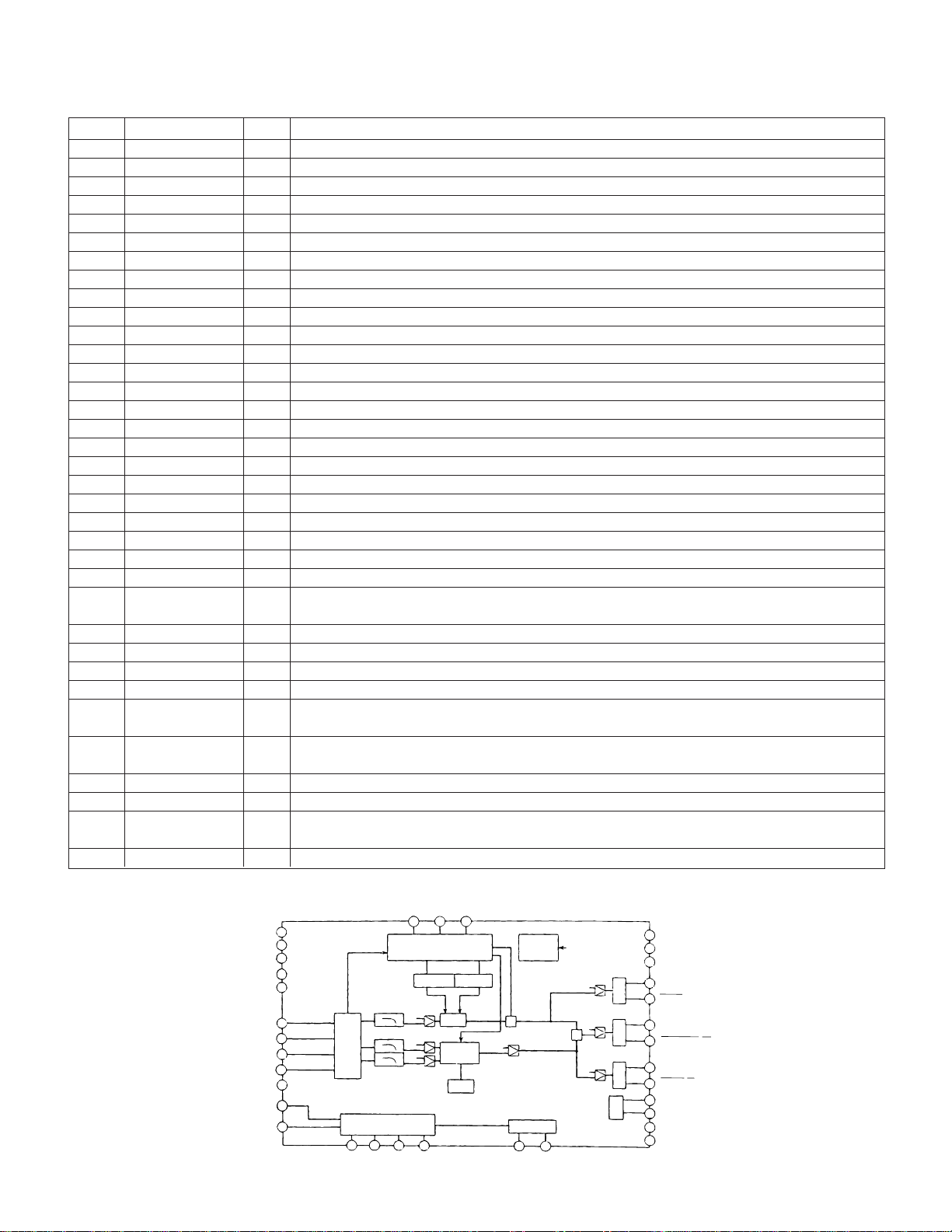
10. IC FUNCTION LIST
10-1. IC201 MC44722A DIGITAL VIDEO DECORDER
Pin No. Terminal name I/O Operation function
1 CVBS/Cb O Analog composite video signal output or Cb signal output current drive (positive)
2 CVBS/Cb O Analog composite video signal output or Cb signal output current drive (negative)
3 CVBS/Cb Vdd Power Supply for CVBS / Cb DAC circuit
4 Y O Analog luminance signal output current drive (positive)
5 Y O Analog luminance signal output current drive (negative)
6 YVdd Power Supply for Y DAC circuit
7 C/Cr O Analog chrominance signal output or Cr signal output current drive (positive)
8 C/Cr O Analog chrominance signal output or Cr signal output current drive (negative)
9 C/CrVdd Power Supply for C/Cr DAC circuit
10 DA Vss Ground for DAC circuit
11 Ibias O Reference current for the 3 DACs
12 DA Vdd Power Supply for DAC circuit
13 VReff Reference full scale voltage for the 3 DACs
14 ChipA I2C chip address select {0 : 42(hex)/43(hex) 1 : 1C(hex)/1D(hex)}
15 TEST I TEST pin (Ground)
16 SO z(O) If SPI mode, serial data output / If I2C mode, connect to ground
17 SDA/SI I/O(I) Serial data input, Open drain output / If SPI mode, serial data input
18 SCL/SCK I Serial clock
19 SEL (I) Connect to Ground / If SPI mode, this pin is chip select
20 DVss Ground for Digital circuit
21 CLOCK I 27MHz clock input
22 DVdd Power Supply for Digital circuit
23 Reset I Reset signal, active LOW
24 PAL/NTSC I NTSC/PAL select. This pin active only Reset time.(NTSC : Low PAL : High)
25-32 DVIN7-0 I 8-bit Multiplexd Y/Cr/Cb 4:2:2 data (ITU Rec656) input (1) or Multiplexd Y data
(ITU-Rec656/601) input in 16-bit input mode (DVIN7 : MSB)
33 TVIN I TEST data input
34 EXT I/O Csync/Frame sync output or external VBI information input
35 F/Vsync I/O Frame sync or Vertical sync input/output
36 Hsync I/O Horizontal sync input/output
37 TP9 I/O MUX switch in 8-bit X 2 Multiplexed Y/Cr/Cb 4:2:2 data (ITU-Rec656) input mode,
or Test data input/output
38-41 TP8-5 I/O 8-bit Multiplexed 4:2:2 data (ITU-Rec656/601) input (2), or Multiplexed Cr/Cb data
(ITU-Rec656/601) input in 16-bit input mode (MSB : TP8), or Test data input/output
42 DVss Ground for Digital circuit
43 DVdd Power Supply for Digital circuit
44-47 TP4-1 I/O 8-bit Multiplexed 4:2:2 data (ITU-Rec656/601) input (2), or Multiplexed Cr/Cb data
(ITU-Rec656/601) input in 16-bit input mode (LSB : TP1), or Test data input/output
48 TP0 I/O For test (should be ground)
DV-A1000U
• Block Diagram
ChipA
DVdd
DVdd
DVss
DVss
DVIN
TP0~7
TVIN
TP9
clock
Reset
PAL/NTSC
14
43
22
20
42
DVIN0~7
32~25
48~44 41~39
33
37
21
23
24
H, V
Y
demux
C
C
b
r
16
12C/SPI
17 18 19
SO
SDA/SI
EXT
34 35 36
Sync_generator
CGM5_gen
0
0
0
SEL
ACL/SCK
F/Vsync
off_set
Modulator
10-1
Hsync
BG
CC_gen
6
DAC
DAC
DAC
BIAS
YVdd
3
CVBS/CbVDD
9
C/CrVdd
4
YOUT
YOUT
5
1
CVBSOUT/Cb
2
CVBSOUT/Cb
7
COUT/Cr
COUT/Cr
8
13
VReff
11
Ibias
12
DAVdd
10
DAVss
copy
bus
protection
0
+
0
TEST
15
TEST
TP0~9
0
+
0
MC44722/3
Page 22
DV-A1000U
10-2. IC301 IX1461GE RF PRE AMP.
Pin No. Terminal name I/O Operation function
1 EIN I RF signal input. Input of RF signal output of optical pickup.
2 GND1 – Ground
3 S/Dsel I Single layer/dual layer selection signal input.
4 AIN I RF signal input. Input of RF signal output of optical pickup.
5 BIN I RF signal input. Input of RF signal output of optical pickup.
6 CIN I RF signal input. Input of RF signal output of optical pickup.
7 DIN I RF signal input. Input of RF signal output of optical pickup.
8 VrefIN I Reference voltage input. (2.1V)
9 FIN I RF signal input. Input of RF signal output of optical pickup.
10 GAINsel1 I Amp gain selection input 1.
11 VCC1 – Power terminal. (5.0V)
12 GAINsel2 I Amp gain selection input 2.
13 FOUT O RF signal output. Input RF signal is current-voltage-converted and output.
14 EOUT O RF signal output. Input RF signal is current-voltage-converted and output.
15 DOUT O RF signal output. Input RF signal is current-voltage-converted and output.
16 COUT O RF signal output. Input RF signal is current-voltage-converted and output.
17 BOUT O RF signal output. Input RF signal is current-voltage-converted and output.
18 AOUT O RF signal output. Input RF signal is current-voltage-converted and output.
19 VCC2 – Power terminal. (5.0V)
20 RFPOUT O Data read signal output. The same phase as MIXIN.
21 RFNOUT O Data read signal output. Reverse phase with respect to MIXIN.
22 MIXIN I Data read signal input.
23 MIXOUT O Data read signal output.
24 GND2 – Ground
• Mode selection table
Single layer/dual layer selection
Layer S/DSEL (Terminal 3) Amp gain
Single L, OPEN 0dB
Dual H +10dB
• Block Diagram
GND2
MIXOUT
MIXIN
24 23 22 21 20 19 18 17 16 15 14 13
MIX
1 98765432 10 1211
EIN
GND1
S/Dsel
RFNOUT
AIN
RFPOUT
BIN
Amp. gain selection
GAINsel1 (Terminal 10) GAINsel2 (Terminal 12) Amp gain
L L +6dB
H, OPEN L -2dB
L H, OPEN +2dB
H, OPEN H, OPEN -6dB
VCC2
CIN
AOUT
DIN
BOUT
VrefIN
COUT
FIN
DOUT
GAINsel1
EOUT
VCC1
FOUT
GAINsel2
10-2
Page 23

10-3. IC303 IX1517GE RF SIGNAL PROCESSOR
DV-A1000U
Pin No. Terminal name I/O Operation function
1 GND – GND terminal. –
2 P2TP I TE+input (CD) VrA
3 P2TN I TE–input (CD) VrA
4 LDO2 O Drive ouput –
5 MDI2 I Monitor input –
6 VrA O Analog VREF 2.1[V]
7 VrD O Digital VREF – Vdd 1/2
8 Vdd I Power terminal 4.2V (3.3V)
9 DPAC – DPD AC combination capacity 1 –
10 DPBD – DPD AC combination capacity 2 –
11 DPD1 – DPD integral capacity 1 –
12 DPD2 – DPD integral capacity 2 –
13 SCB I Control line (Bit clock) 2.2[V]
14 SCL I Control line (Latch signal) 2.2[V]
15 SCD I Control line (Sirial Data) 2.2[V]
16 VRCK I Reference clock input 2.3[V] When frequency is increased, the
17 VCKF –
18 VccP – Power terminal –
19 LVL O Servo addition output Vrd x (1/2)
20 TEO O TE output VrD
21 FEO O FE output VrD
22 DFTN I DPD difect – Low DPD output: Mute
23 VccS – Power terminal (servo) –
24 RPZ O RF ripple center voltage VrD
25 RPO O RF ripple output VrD
26 RPB O RF ripple bottom –
27 RPP O RF ripple peak –
28 RFO O Equalizing RF output 2.3[V]
29 NC – NC terminal – To be connected to GND
30 NC – NC terminal – To be connected to GND
31 VccR – Power terminal (RF) –
32 DPDB I Pit depth adjustment VrD When D PDB is raised, the A/B
33 TEB I TE balance VrD When TEB is raised, the TP side
34 FEB I FE balance VrD When FEB is raised, the A+C (FP)
35 PSC I VRCK frequency division ON/OFF – High: Frequency division OFF
36 Vcc2 – Power terminal –
37 NC – NC terminal VrD To be connected to VrD, or to GND
38 EQD I Group delay correction VrD When EQD is raised, the group
39 GND2 – GND terminal. –
40 RFDC – DC feedback capacity –
41 RFA O RF total addition output 2.2[V]
42 EQB I Boost adjustment VrD
43 EQF I Frequency adjustment VrD When EQF is raised, shift to the
44 MDI1 I Monitor input –
45 LDO1 O Drive output –
46 P1TN I TE–input (DVD) VrA
47 P1TP I TE+input (DVD) VrA
48 NC – NC terminal – To be connected to GND
49 P1FN I FE–input (DVD) VrA
50 P1TP I FE+input (DVD) VrA
51 LDP1 I APC polarity 1 – Positive polarity when this terminal
52 P1DI I D input (DVD)
Capacity for time constant adjustment
Terminal DC Voltage(TYP.)
–
Remarks
filters excepting the servo LPF are
shifted to high frequency side.
side delay increases.
gain increases and the A+C side
delay increases.
side gain increases.
through C
delay increases at the right side.
When EQB is raised, the boost increases.
high frequency side occurs.
is connected to Vcc.
10-3
Page 24
DV-A1000U
Pin No. Terminal name I/O Operation function
Terminal DC Voltage(TYP.)
Remarks
53 P1CI I C input (DVD) VrA
54 P1BI I B input (DVD) VrA
55 P1AI I A input (DVD) VrA
56 GNDR – GND terminal (RF) –
57 LDP2 I APC polarity 2 – Positive polarity when this terminal
is connected to Vcc.
58 P2AI I A input (CD) VrA
59 P2BI I B input (CD) VrA
60 P2CI I C input (CD) VrA
61 P2DI I D input (CD) VrA
62 GNDS – GND terminal (Servo) –
63 P2FP I FE+input (CD) VrA
64 P2FN I FE–input (CD) VrA
• Block Diagram
NC
P1TP
P1TN
LDO1
MDI1
EQF
EQB
RFA
RFDC
GND2
P1FN
P1FP
LDP1
P1DI
P1CI
P1BI
P1AI
GNDR
LDP2
P2AI
P2BI
P2CI
P2DI
GNDS
P2FP
P2FN
EQDNCVcc2
48 47 46 45 44 43 42 41 40 39 38 37 36 35 34 33
49
APC1
50
51
52
53
sel-RF
R-gain
Adjust
EQ
54
55
56
57
58
59
60
61
62
63
64
sel-PD
sel-PD
sel-PD
F-gain
Adjust
F-gain
Adjust
sel-DPD
T-gain
Adjust
APC2
RF Ripple
sel-IC
sel-FE
FE creation
sel-TE
DPDTE
creation
sel-LVL
3BTE creation
creation
mode-TE
B U S
PSC
FE-gain
Adjust
TE-gain
Adjust
Level detect
FEB
Time
constant
adjustment
TEB
32
31
30
29
28
27
26
25
24
23
22
21
20
19
18
17
DPDB
VccR
NC
NC
RFO
RPP
RPB
RPO
RPZ
VccS
DFTN
FEO
TEO
LVL
LccP
VCKF
12345678910111213141516
GND
P2TP
P2TN
LDO2
MDI2
10-4. IC401 IX1484GE 4M DRAM
Terminal
10~13,16~20,9 A0~A8,A9R Address input
8 RAS Row address strobe
23 CAS Column address strobe
1~5,24~27 DQ1~DQ8 Data input/Data output
22 OE Output enable
7 WE Light enable
1 Vcc Power (5V)
28 Vss Ground (0V)
21 NC Not connected
Terminal name Function
VrA
VrD
Vdd
10-4
DPAC
DPBD
DPD1
DPD2
SCB
SCL
SCD
SRCK
Page 25

10-5. IC402 IX1474GE DEM/ECC (DVD)
Pin No. Terminal name I/O Operation function Remarks
1 DPCK1 I Signal processing reference clock input. 0.5-3.3Vp-p Feedback
resistor built in.
2 DVDD3 – Digital power. (3.3V) For logic cell
3 SVCK1 I Servo reference clock input. (Oscillation circuit input terminal) 3.3V-I/F Feedback
4 SVCK0 O Servo reference clock output. (Oscillation circuit input terminal) resistor built in.
5 DVSS – Digital power. (0V) For logic cell
6 DVDD2 – Digital power. (3.3V) For logic cell
7 N.C. – User use prohibited. Open
8 HDWT I MPU write signal. TTL level
9 HDRD I MPU read signal. TTL level
10 HCEN I MPU chip selection. TTL level
11 HD0 I/O MPU data bus. TTL level
12 HD1 I/O MPU data bus. TTL level
13 HD2 I/O MPU data bus. TTL level
14 HD3 I/O MPU data bus. TTL level
15 HD4 I/O MPU data bus. TTL level
16 HD5 I/O MPU data bus. TTL level
17 HD6 I/O MPU data bus. TTL level
18 HD7 I/O MPU data bus. TTL level
19 DVSS – Digital power. (0V) For I/O cell
20 DVDD5 – Digital power. (5V) For I/O cell
21 HINT O MPU interruption signal. (Occurrence of interruption = “L”) OPEN DRAIN
22 HA0 I MPU address bus. TTL level
23 HA1 I MPU address bus. TTL level
24 PLCK I/O Read channel clock input/output terminal.
25 ED0 – User use is prohibited (N.C.) since it is for shipping adjustment. Open
26 ED1 –
27 ED2 –
28 ED3 –
29 ED4 –
30 ED5 –
31 ED6 –
32 ED7 –
33 TEST I For shipping adjustment. Set to “L”
34 PDON O PLL phase error signal output. (Negative polarity)
35 PDOP O PLL phase error signal output. (Positive polarity)
36 RLLD O RLL detection result output.
37 LPFN I PLL loop filter amp. reverse input.
38 LPFO O PLL loop filter amp. output.
39 VCOF O VCO filter terminal.
40 SLCO O Built-in comparator reference voltage output terminal.
41 AVSS – Analog power. (0V)
42 AVR O Non-PLL system analog reference potential. (1.65V)
43 VRC – Resistance division point potential. (For analog reference
potential generation: 1.65)
44 PVR O PLL system analog reference potential. (1.65V)
45 AVDD – Analog power. (3.3V)
46 RVR2 – 2nd reference voltage. (For capacitor connection)
47 RVDD – Exclusive-use power terminal. (3.3V)
48 RFIN I RF signal input.
49 RVSS – Exclusive-use power terminal. (0V)
50 RVR1 – 1nd reference voltage. (For capacitor connection)
51 DVR I DMO reference potential. (1.65V recommended)
52 DMO O Disc equalizer output for DVD. (Triple value PWM + HiZ)
53 RASN O External RAM row address selection. (Negative logic)
54 CASN O External RAM row address selection. (Negative logic)
DV-A1000U
10-5
Page 26

DV-A1000U
Pin No. Terminal name I/O Operation function Remarks
55 MOEN O External RAM output permission signal.
56 MWEN O External RAM read/write selection.
57 DVSS – Digital power. (0V) For logic cell
58 DVDD3 – Digital power. (3.3V) For logic cell
59 MA9 O External RAM address bus.
60 MA8 O External RAM address bus.
61 MA7 O External RAM address bus.
62 MA6 O External RAM address bus.
63 MA5 O External RAM address bus.
64 MA4 O External RAM address bus.
65 MA3 O External RAM address bus.
66 MA2 O External RAM address bus.
67 MA1 O External RAM address bus.
68 MA0 O External RAM address bus.
69 DVSS – Digital power. (0V) For I/O cell
70 DVDD5 – Digital power. (5V) For I/O cell
71 MD7 I/O External RAM data bus. TTL level
72 MD6 I/O External RAM data bus. TTL level
73 MD5 I/O External RAM data bus. TTL level
74 MD4 I/O External RAM data bus. TTL level
75 MD3 I/O External RAM data bus. TTL level
76 MD2 I/O External RAM data bus. TTL level
77 MD1 I/O External RAM data bus. TTL level
78 MD0 I/O External RAM data bus. TTL level
79 SD7 O MPEG data output.
80 SD6 O MPEG data output.
81 SD5 O MPEG data output.
82 SD4 O MPEG data output.
83 DVSS – Digital power. (0V) For logic cell
84 DVDD3 – Digital power. (3.3V) For logic cell
85 SD3 O MPEG data output.
86 SD2 O MPEG data output.
87 SD1 O MPEG data output.
88 SD0 O MPEG data output.
89 SERR O MPEG data reliability flag. (Data error: “L”)
90 SBGN O MPEG output sector sync signal. (Sector top: “L”)
91 SENB O MPEG data effective flag. (Effective state: “L”)
92 SDCK O MPEG data transfer clock.
93 DVSS – Digital power. (0V) For logic cell
94 SREQ I MPEG data request flag. (Request state: “L”) TTL level
95 RSTN I Hard reset input. (Reset state: “L”)
96 DVDD3 – Digital power. (3.3V) For logic cell
97 STDA O Operation state monitor data. Common with PWM.
(Output synchronizing with SDCK fall)
98 STCK O Operation state monitor sync signal. (Data top bit: “L”) Common with PWM.
99 UPWM O General-use PWM output. 4mA, 5V-I/F
100 DVSS – Digital power. (0V) For logic cell
10-6
Page 27
DV-A1000U
ID
Register
CSR
ESRs
DQ
8-15
DQ
0-7
OUTPUT MULTIPLEXER
Program Erase
Voltage Switch
BYTE#
CUIWSM
16-KBYTE
Block 31
16-KBYTE
Block 30
16-KBYTE
Block 1
16-KBYTE
Block 0
CE#
OE#
WE#
RP#
RY/BY#
V
PP
V
CC
GND
Y GATING/SENSING
X-DECODER
Y-DECODER
Input
Buffer
ADDRESS
QUEUE
LATCHES
ADDRESS
COUNTER
A
-1.0~17
Output
Buffer
Output
Buffer
Input
Buffer
Input
Buffer
I/O Logic
DATA
QUEUE
REGISTER
Register
Data
Comparator
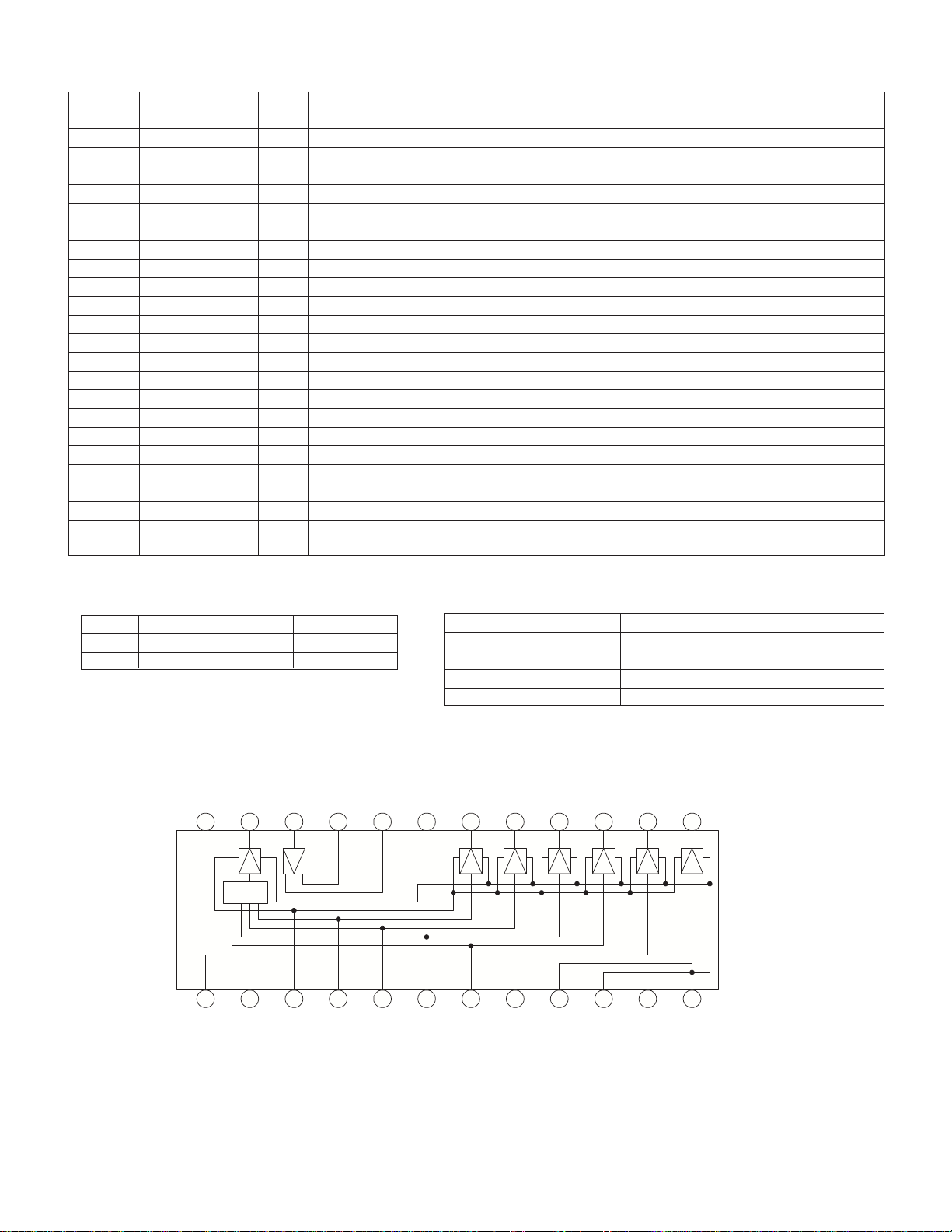
10-6. IC501 IX1518GE FLASH
Terminal Symbol Type Name and function
Byte selection address: When the device is in the x8 mode, the low or high order byte is
45 DQ
25~18,
8~4 latched during data wiring operation.
3~1,
48,17 during data writing, erasing and lock block operation.
A
A
13-A17
15/A-1
0-A12
29, 31, 33 Low order byte data input/output: Command user interface writing cycle data and command
35, 38, 40, DQ
-DQ7Input/Output
0
42, 44 disable: Float state
30, 32, 34, 36,
39, 41, 43, 45
DQ8-DQ15Input/Output
26 CE# Input
12 RP# Input
28 OE# Input
11 WE# Input
15 RY/BY# Output
47 BYTE# Input the DQ
13 Vpp Wr ite/erase power supply: 5.0 ± 0.5V is applied during writing/erasing.
37 Vcc Device power supply: 5.0 ± 0.5V
27, 46 GND Ground
9, 10, 14, 16 NC Nonconnection
Input selected. It is not used in the x16 mode.
(If BYTE# is high, DQ15/A-1 input circuit does not operate.)
Input
Input
Word selection address: Selection of one word of 16k byte block. These addresses are
Block selection address: Selection of 1/32 erase block. These addresses are latched
input. Various data read memory identifier and status data output Chip nonselection or output
High order byte data input/output: The function is the same as that of low order byte data
input/output. Operative only in x16 mode. x8 mode: Float state DQ15/A-1 is address.
Chip enable: Device control logic, input buffer, decoder and sense amp. are activated.
Chip becomes active only when CE# is “Low”.
Reset/Power down: If RP# is set to “Low”, the control circuit is initialized when power
is turned on. Hence, the RP#pin is set to “Low”. When power is turned on or off or in
case of fluctuation it is kept at “Low” so as to protect data from noise. When RP# is in
“Low” state, the device is in deep power down state. 480 ns is required to recover
from the deep power down state. If the RP# pin becomes “Low”, the whole chip operation is
interrupted and reset. After recovery the device is set to array read state.
Output enable: When OE# is set to “Low”, data is output from the DQ pin. When OE# is
set to “High”, the DQ pin is set to float state.
Write enable: Command user interface, data Q register and address Q latch access is
controlled. In “Low” state WE# becomes active. At rise edge the address and data are fetched.
Ready/busy: The state of internal write state machine is output. In “Low” state it is indicated
that the write state machine is in operation. If the write state machine waits for next operation
instruction, erase is suspended or it is in deep power down state, the RY/BY# pin is in float state.
Byte enable: When BYTE# is set to “Low”, the device is set to the x8 mode. At this time
-DQ15 pin becomes float state. Address A-1 selects high order/low order byte.
8
When BYTE# is “High”, the device is set to the x16 mode. The A-1 input circuit is disabled.
• Block Diagram
10-7
Page 28
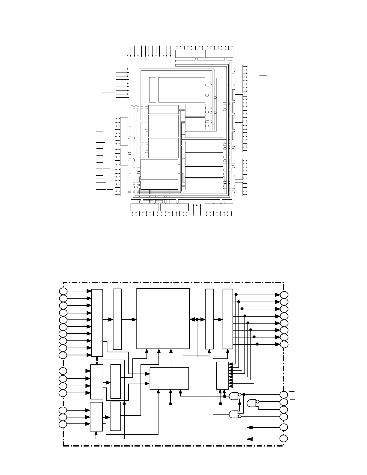
DV-A1000U
10-7. IC504 IX1478GE SYSCON
VccVccVccVccVccVssVssVssVssVssVssVssVssPD
15
14
13
12
11
10
9
8
7
6
5
4
3
2
1
/D
/D
/D
/D
/D
/D
/D
/D
/D
/D
7
6
5
4
3
2
PD
PD
PD
PD
PD
Port D
/D
1
0
7
6
PD
PD
PE
PE
PE
Port E
0
/D
/D
/D
/D
/D
5
4
3
2
1
0
PE
PE
PE
PE
PE
MD
2
MD
1
MD
0
EXTAL
XTAL
STBY
RES
WDTOVF
NMI
PF7/ø
PF
/AS
6
PF
/RD
5
PF
/HWR
4
PF3/LWR
PF2/
LCAS/WAIT/BFEQO
PF1/BACK
PF0/BREQ
PG4/CS0
PG3/CS1
PG2/CS2
PG1/CS3
PG0/CAS
P67/CS7/IRQ3
P66/CS6/IRQ2
P65/IRQ1
P64/IRQ0
P63/TEND1
P62/DREQ1
P61/TEND0/CS5
P60/DREQ0/CS4
H8S/2000 CPU
Clock oscillator
Interruption
controller
*
ROM
Port FPort GPort 6
RAM
TPU
PPG
Port 1 Port 2 Port 4
DTC
DMAC
WDT
SCI
D/A converter
A/D converter
ss
ref
V
AVccAV
Internal data bus
Internal address bus
/AN7/DA1
/AN6/DA0
/AN5
7
6
5
P4
P4
P4
Bass Controller
Peripheral data bus
/AN4
/AN3
/AN2
/AN1
4
3
2
1
P4
P4
P4
P4
Peripheral address bus
Port 5 Port 3 Port C Port B Port A
/AN0
0
P4
PA7/A23/IRQ7
/IRQ6
PA
6/A22
PA5/A21/IRQ5
PA4/A20/IRQ4
PA
3/A19
PA2/A
18
PA1/A
17
PA0/A
16
PB7/A
15
PB6/A
14
PB5/A
13
PB4/A
12
PB3/A
11
PB2/A
10
PB1/A
9
PB0/A
8
PC7/A
7
PC6/A
6
PC5/A
5
PC4/A
4
PC3/A
3
PC2/A
2
PC1/A
1
PC0/A
0
P35/SCK1
/SCK0
P3
4
P3
/RxD1
3
/RxD0
P3
2
P3
/TxD1
1
P3
/TxD0
0
P5
0
P5
1
P5
2
P53/ADTRG
/PO8/TIOCA0/DACK0
/PO9/TIOCB0/DACK1
0
1
P1
P1
10-8. IC506 M51008BF 1M SRAM
8
A4
7
A5
6
A6
5
A7
4
A12
A14
A16
A15
A13
A10
A11
3
2
ADDRESS INPUT
31
28
27
A8
12
A0
10
A2
9
A3
23
11
A1
ADDRESS INPUT
25
A9
26
ADDRESS INPUT
BUFFER
BUFFER
BUFFER
ROW
DECORDER
COLUMN
DECODER
BLOCK
DECODER
/PO0/TIOCA3
/PO1/TIOCB3
0
/PO10/TIOCC0/TCLKA
/PO11/TIOCD0/TCLKB
/PO12/TIOCA1
2
3
4
P1
P1
P1
131072 WORDS
X 8 BYS
(1024 ROWS
X126 COLUMNS
X8 BL9OCKS)
1
/PO13/TIOCB1/TCLKC
/PO14/TIOCA2
/PO15/TIOCB2/TCLKD
5
6
7
P2
P2
P1
P1
P1
CLOCK
GENERATOR
/PO2/TIOCC3
/PO3/TIOCD3
/PO4/TIOCA4
/PO5/TIOCB4
/PO6/TIOCA5
2
3
4
5
P2
P2
P2
P2
P2
/PO7/TIOCB5
6
7
P2
SENSE AMP.
BUFFER
DATA INPUT
BUFFER
OUTPUT
24
32
16
13
14
15
17
18
19
20
21
29
22
30
DQ1
DQ2
DQ3
DQ4
DQ5
DQ6
DQ7
W
S1
S2
OE
VCC
(5V)
GND
(0V)
10-8
Page 29
10-9. IC507/5002 BR93L46F EEPROM
Terminal Terminal name In/Output Function
2 VCC – Power
7 GND – All input/output reference voltage, 0V
3 CS Input Tip select input
4 SK Input Sirial clock input
5 DI Input Start bit, operation code, address and serial data input
6 DO Output Serial data output, READY/BUSY internal status indication output
• Block Diagram
Wave voltage
C S
Instruction decode control
clock generation
S K
detection
Write
inhibition
High voltage
generation
DV-A1000U
D I
D O
Instruction
register
Dummy bit
Address
buffer
Data
resistor
6bit
16bit
Address
Decoder
R/W
Amp.
6bit
16bit
10-10. IC508 IX1516GE GAMMA S-P-TONE
Terminal Terminal name In/Output Function
1 VCC – Digitan power +3.3V
2 HADR (0) Input CPU Address bus
3 HADR (1) Input CPU Address bus
4 HADR (2) Input CPU Address bus
5 HADR (3) Input CPU Address bus
6 HADR (4) Input CPU Address bus
7 HADR (5) Input CPU Address bus
8 VSS – Digital GND
9 VCC – Digitan power +3.3V
10 HADR (6) Input CPU Address bus
11 HADR (7) Input CPU Address bus
12 HADAT (0) Input CPU Data bus
13 HADAT (1) Input CPU Data bus
14 HADAT (2) Input CPU Data bus
15 HADAT (3) Input CPU Data bus
16 VSS – Digital GND
17 VCC – Digitan power +3.3V
18 HADAT (4) Input CPU Data bus
19 HADAT (5) Input CPU Data bus
20 HADAT (6) Input CPU Data bus
21 HADAT (7) Input CPU Data bus
22 NC NC –
23 NC NC –
24 VSS – Digital GND
25 VCC – Digitan power +3.3V
26 HRD Input CPU read signal
27 HWR Input CPU write signal
28 HAS Input CPU address strobe signal
29 HCS Input CPU tip select signal
30 HIM Input CPU bus control selection signal (I/M mode = H/L)
1,024
bit
EEPROM
Aray
10-9
Page 30
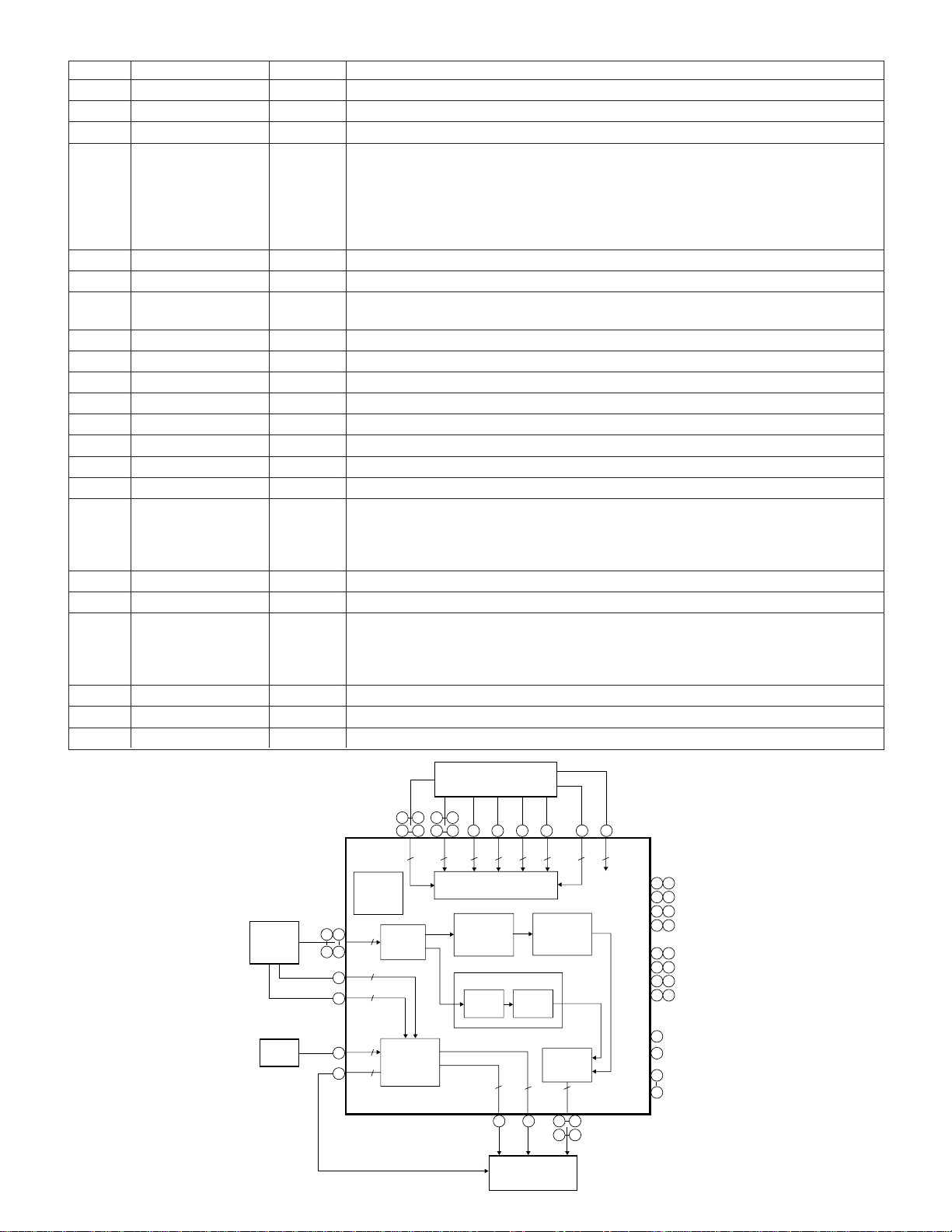
DV-A1000U
Terminal
Terminal name In/Output Function
31 MRST Input Reset signal
32 VSS – Digital GND
33 VCC – Digital power +3.3V
34 PXDO (0) Output Pixel data output
35 PXDO (1) Output
8-bit parallel video data conforming to ITU-R BT.601 and BT.656 standard (Cb/Y/Cr/Y)
36 PXDO (2) Output MSB=PXDO(7), LSB=PXDO(0)
37 PXDO (3) Output
38 PXDO (4) Output
39 PXDO (1) Output
40 VSS – Digital GND
41 VCC – Digital power +3.3V
42 PXDO (6) Output
43 PXDO (7) Output
44 CKO Output Reference clock output for pixel data. 27 MHz
45 VDO Output Vertical sync signal output
46 HDO Output Horizontal sync signal output
47 VDI Input Vertical sync signal output
48 VSS – Digital GND
49 VCC – Digital power +3.3V
50 HDI Input Horizontal sync signal output
51 CKI Input Reference clock output for pixel data. 27 MHz
52 PXDI (0) Input Pixel data output
53 PXDI (1) Input
8-bit parallel video data conforming to ITU-R BT.601 and BT.656 standard (Cb/Y/Cr/Y)
54 PXDI (2) Input MSB=PXDI(7), LSB=PXDI(0)
55 PXDI (3) Input
56 VSS – Digital GND
57 VCC – Digital power +3.3V
58 PXDI (4) Input
59 PXDI (5) Input
60 PXDI (6) Input
61 PXDI (7) Input
62 TEST1 Input Test terminal
63 TEST2 Input Test terminal
64 VSS – Digital GND
• Block Diagram
Source
Dec.
Clock
Gen.
52 58
55 61
PXDI
HDI
50
VDI
47
CKI
51
CKO
44
64pin LQFP
HDAT
Edge
creation
SPT circuit
ITU-R
601/656
interface
1
1
Timing
1
generation
1
CPU
12
16
27
21 29 28 27 26 30 31
18
10 11
HDAR IICS IIAS HWR HRD HIM MRST
8881
111 11
Host interface
Digital
dinamic
r circuit
Digital color correction
White
correction
Color
offset
correction
11
4546
NTSC Enc.
(3ch D/A built in)
DR-SPT
circuit
ITU-R
601/656
formatter
8
PXDOVDDHDO
42
3934
43
10-10
VCC
VSS
TEST1
TEST2
NC
19
171625
33
49 57
8
24 32
40 48
56 54
62
63
22
23
41
Page 31

10-11. IC512 IX1535GE HOST I/F
Terminal Terminal name In/Output Function
1 VDD – Power +3.3V
2 HADR0 Input CPU Address bus
3 HADR1 Input CPU Address bus
4 HADR2 Input CPU Address bus
5 HCS Input CPU Tip select
6 HWR Input CPU Write signal
7 HRD Input CPU Read signal
8 HDAT0 In/Output CPU Data bus
9 HDAT1 In/Output CPU Data bus
10 HDAT2 In/Output CPU Data bus
11 HDAT3 In/Output CPU Data bus
12 HDAT4 In/Output CPU Data bus
13 HDAT5 In/Output CPU Data bus
14 HDAT6 In/Output CPU Data bus
15 HDAT7 In/Output CPU Data bus
16 VSS – Digital GND
17 VDD – Power +3.3V
18 EXPAL (0) In/Output General-use input/output terminal Gr.A
19 EXPAL (1) In/Output General-use input/output terminal Gr.A
20 EXPAL (2) In/Output General-use input/output terminal Gr.A
21 EXPAL (3) In/Output General-use input/output terminal Gr.A
22 EXPAU (0) In/Output General-use input/output terminal Gr.A
23 EXPAU (1) In/Output General-use input/output terminal Gr.A
24 VSS – Digital GND
25 VDD – Power +3.3V
26 EXPAU (2) In/Output General-use input/output terminal Gr.A
27 EXPAU (3) In/Output General-use input/output terminal Gr.A
28 EXPBL (0) In/Output General-use input/output terminal Gr.B
29 EXPBL (1) In/Output General-use input/output terminal Gr.B
30 EXPBL (2) In/Output General-use input/output terminal Gr.B
31 EXPBL (3) In/Output General-use input/output terminal Gr.B
32 VSS – Digital GND
33 VDD – Power +3.3V
34 EXPBU (0) In/Output General-use input/output terminal Gr.B
35 EXPBU (1) In/Output General-use input/output terminal Gr.B
36 EXPBU (2) In/Output General-use input/output terminal Gr.B
37 EXPBU (3) In/Output General-use input/output terminal Gr.B
38 EXPC (0) In/Output General-use input/output terminal Gr.C
39 EXPC (1) In/Output General-use input/output terminal Gr.C
40 EXPC (2) In/Output General-use input/output terminal Gr.C
41 VSS – Digital GND
42 EXPC (3) In/Output General-use input/output terminal Gr.C
43 EXPC (4) In/Output General-use input/output terminal Gr.C
44 EXPC (5) In/Output General-use input/output terminal Gr.C
45 EXPD (0) In/Output General-use input/output terminal Gr.D
46 EXPD (1) In/Output General-use input/output terminal Gr.D
47 EXPD (2) In/Output General-use input/output terminal Gr.D
48 VSS – Digital GND
49 VDD – Power +3.3V
50 EXPD (3) In/Output General-use input/output terminal Gr.D
51 EXPD (4) In/Output General-use input/output terminal Gr.D
52 EXPD (5) In/Output General-use input/output terminal Gr.D
53 BUFDO Output Buffer output D
54 BUFDI Input Buffer input D
55 SBUFBO Output Schmidt buffer output B
56 SBUFBI Input Schmidt buffer input B
57 SBUFAO Output Schmidt buffer output A
58 SBUFAI Input Schmidt buffer input A
59 MRST Input Reset terminal
60 MODE Input Mode selection terminal
61 BUFCO In/Output Buffer output C
62 TEST Input Test terminal (for Epson)
63 BUFCI Input Buffer input C
64 VSS – Digital GND
DV-A1000U
10-11
Page 32

DV-A1000U
Pin1~15........There is a possibility of simultaneous change. Operating frequency: Approx. 10 MHz
Pin18~47 ..... There is a possibility of simultaneous change.(Static signal) Operating frequency: Approx. 1 MHz
Pin50~57 ..... There is almost no possibility of simultaneous change. Operating frequency: Approx. 1 MHz
Pin63............ Not used
• Block Diagram
In/Output Pin
VDD
SOUT(3)
SOUT(4)
SOUT(5)
Exclusive-use pin
MRST
MODE
SEL
TEST
CK
VSS
VDD
EXPD(3)
EXPD(4)
EXPD(5)
BUFDO
BUFDI
SBUFBO
SBUFBI
SBUFAO
SBUFAI
MRST
MODE
BUFCO
TEST
BUFCI
VSS
In/Output Pin
Output:
S2(5)
SOUT(0)
EXPD(0)
EXPC(5)
HCS
S2(4)
EXPC(4)
HWR
HRD
Open drain
VSS
S2(3)
VSS
EXPC(3)
Data Buffer
Latch C
Data Buffer
HDAT0
HDAT1
In/Output Pin
VSS
SOUT(2)
SOUT(1)
VSS
EXPD(2)
EXPD(1)
48
47 46 45 44 43 42 41 40 39 38 37 36 35 34 33
49
50
51
52
53
54
55
56
57
58
59
60
61
62
63
64
Data Buffer
Latch D
R/W CTL
VDD
HADR0
HADR1
HADR2
S2(2)
S2(1)
EXPC(2)
EXPC(1)
HDAT2
S2(0)
EXPC(0)
HDAT3
HDAT4
In/Output Pin
Q2(7)
Q2(6)
Q2(5)
EXPBU(3)
EXPBU(2)
EXPBU(1)
Data Buffer
Latch B
Data Buffer
Latch A
HDAT5
HDAT6
Q2(4)
EXPBU(0)
16151413121110987654321
VSS
HDAT7
VDD
VDD
32
31
30
29
28
27
26
25
24
23
22
21
20
19
18
17
VSS
EXPBL(3)
EXPBL(2)
EXPBL(1)
EXPBL(0)
EXPAU(3)
EXPAU(2)
VDD
VSS
EXPAU(1)
EXPAU(0)
EXPAL(3)
EXPAL(2)
EXPAL(1)
EXPAL(0)
VDD
VSS
Q2(3)
Q2(2)
Q2(1)
Q2(0)
Q1(7)
Q1(6)
VDD
VSS
Q1(5)
Q1(4)
Q1(3)
Q1(2)
Q1(1)
Q1(0)
VDD
In/Output Pin
D(0)
D(1)
D(2)
D(3)
D(4)
D(5)
D(6)
VDD
Input Pin
D(7)
S1(0)
S1(1)
In/Output Pin
S1(2)
S1(3)
S1(4)
S1(5)
VSS
Output: Open drain
10-12. IC601 IX1521GE SOURCE DECODER
Pin No. Pin name Type Direction Function
Microcomputer interface
22
24-26 Used for register access and so on
27
HA[3:0] I I
HWR#
(HR/W#) HTYPE = H
II
29 HCS# I I Chip select input for connection to microcomputer
30
HRD#
(HDS#) HTYPE = H
II
31 HRDY 3-S O Bit stream can not be input.
Address bus input for microcomputer connection.
HTYPE = L
It works as HR/W#(read/write) input terminal for connection to Motorola
type microcomputer.
It works as HWR# (write) input terminal for connection to general purpose
microcomputer.
HTYPE = L
It works as HDS#(data strobe) input terminal for connection to Motorola
type microcomputer.
It works as HRD# (read) input terminal for connection to general purpose
microcomputer.
Bit stream input ready output terminal If the bit stream is input from
microcomputer, the terminal is bored.
For 3-state output, connect the pull-up resistor.
HRDY = L
HRDY = H
The number of bytes which are set by CodBurstLen parameter can be
transferred from the microcomputer. During the time from transfer start of
the number of set bytes to transfer end, the terminal varies in 3 states.
10-12
Page 33

Microcomputer interface terminal list
Pin No. Pin name Type Direction Function
Microcomputer interface
HTYPE = L
It works as HACK# (acknowledge) output terminal for connection to
32 HACK# Motorola type microcomputer.
(HR/W#) It can be used as the weight terminal for connection to the general pur
pose microcomputer. For 3-state output, connect the pull-up resistor.
Interrupt request. If interrupt status register is read, interrupt is masked or
34 HIRQ# 3-S O device is reset, the signal is deasserted.
For 3-state output, connect the pull-up resistor.
The bus width of the microcomputer interface If the device is worked as
CD-G decoder or CD-DSP is connected, select the 8-bit bus mode.
35 HWID I I Fix it before power up.
L=8bit bus mode
H=16bit bus mode
When HWID is H (16-bit bus MODE), byte order is set.
Setting is valid only when HWID is H.
36 HORD I I Fix it before power up.
L=HD [15:8] is regarded as m.s. byte. (Motorola type)
H=HD [7:0] is regarded as m.s. byte. (Intel type)
Bus type of microcomputer interface is set.
37 HTYPE I I
141 RESET# I I RESET is input.
142 IDLE 3-S O It is output to indicate the idle state.
Fix it before power up.
L=Motorola type
H=General purpose type
DV-A1000U
Microcomputer / CD·subcode interface terminal list
Pin No. Pin name Type Direction Function
Microcomputer interface / CD·subcode interface
When 16-bit bus width is selected, (HWID=low)
3
4
5
6
7
9 HD10 3-S I/O
HD15 3-S I/O
(CDCLK) (I) (I)
HD14 3-S I/O
(CDDAT) (I) (I)
HD13 3-S I/O
(CDFRM) (I) (I)
HD12 3-S I/O
(CDERR) (I) (I)
HD11 3-S I/O
(SCCLK) (O) (O)
(SCDAT) (I) (I)
It works as the microcomputer data bus of 15th bit.
When 8-bit bus width is selected, (HWID=high)
It works as the terminal to input bit clock from DC-DSP.
When 16-bit bus width is selected, (HWID=low)
It works as the microcomputer data bus of 14th bit.
When 8-bit bus width is selected, (HWID=high)
It works as the terminal to input the stream/PCM data from CD-DSP.
When 16-bit bus width is selected, (HWID=low)
It works as the microcomputer data bus of 13th bit.
When 8-bit bus width is selected, (HWID=high)
It works as the terminal to input frame synchronous signal from CD-DSP.
When 16-bit bus width is selected, (HWID=low)
It works as the microcomputer data bus of 12th bit.
When 8-bit bus width is selected, (HWID=high)
It works as the terminal to input error signal to CD-DSP.
When 16-bit bus width is selected, (HWID=low)
It works as the microcomputer data bus of 11th bit.
When 8-bit bus width is selected, (HWID=high)
It works as the terminal to output the subcode reading clock to the
subcode interface of CD-DSP.
When 16-bit bus width is selected, (HWID=low)
It works as the microcomputer data bus of 10th bit.
When 8-bit bus width is selected, (HWID=high)
It works as the terminal to input subcode data from subcode interface ofCD-DSP.
Pin No. Pin name Type Direction
General port
2 GPSI I I
122-123 GPAIO[1:0] 3-S I/O
159 GPSO O O
General port terminal list
Function
General purpose terminal.
General input/output terminal. After resetting, it becomes the input direction.
General output terminal.
10-13
Page 34

DV-A1000U
Microcomputer / CD·subcode interface terminal list
Pin No. Pin name Type Direction Function
Microcomputer interface / CD·subcode interface
When 16-bit bus width is selected, (HWID=low)
10
11
12
14-17 HD[7:0] 3-S I/O
19-21
Pin No. Pin name Type Direction
Pin No. Pin name Type Direction Function
PLL interface
126 GCLK1 I I
128 XO O O
129 GCLK I I
135, 137
136 PLLCA – –
HD9 3-S I/O
(SCSYN) (I) (I)
HD8 3-S I/O
(SCFRM) (I) (I)
PLLCFG[1:0] I I
It works as the microcomputer data bus of 9th bit.
When 8-bit bus width is selected, (HWID=high)
It works as the terminal to input the subcode synchronous signal from the
subcode interface of CD-DSP.
When 16-bit bus width is selected, (HWID=low)
It works as the microcomputer data bus of 9th bit.
When 8-bit bus width is selected, (HWID=high)
It works as the terminal to input the frame synchronous signal from the
subcode interface of CD-DSP.
It works as the microcomputer bus of bits 7 thru 0.
PLL interface terminal list
Test terminal. Don’t connect it.
If quartz oscillator is connected to GCLK terminal, connect the other
terminal of quartz oscillator to this pin.
Master clock input terminal of device Input 27 MHz.
PLL is set. Before power-up, fix it.
External capacitor terminal for PLL.
Video/OSD interface terminal list
Pin No. Pin name Type Direction
Pin No. Pin name Type Direction Function
Video interface · OSD interface
102
104
105
106
107
C7 3-S O
(N.C.) (3-S) (O)
C6 3-S O
(N.C.) (3-S) (O)
C5 3-S O
(N.C.) (3-S) (O)
C4 3-S O
(OSDPLT) (3-S) (I)
C3 3-S O
(OSDPEL3) (3-S) (I)
Video8 register = 0
Color difference signal output terminal of 7th bit.
Video8 register = 1
The terminal becomes invalid.
Video8 register = 0
Color difference signal output terminal of 6th bit.
Video8 register = 1
The terminal becomes invalid.
Video8 register = 0
Color difference signal output terminal of 5th bit.
Video8 register = 1
The terminal becomes invalid.
Video8 register = 0
Color difference signal output terminal of 4th bit.
Video8 register = 1
Input terminal to select pallet table of OSD.
For OSDPLT=low, pallet table 0 is used.
For OSDPLT=high, pallet table 1 is used.
Video8 register = 0
Color difference signal output terminal of 3th bit.
Video8 register = 1
It works as the OSD pallet data input terminal of 3rd bit.
10-14
Page 35

Video/OSD interface terminal list
Pin No. Pin name Type Direction Function
Video interface · OSD interface
109
110
111
C2 3-S O
(OSDPEL2) (3-S) (I)
C1 3-S O
(OSDPEL1) (3-S) (I)
C0 3-S O
(OSDPEL0) (3-S) (I)
Video8 register = 0
Color difference signal output terminal of 2th bit.
Video8 register = 1
It works as the OSD pallet data input terminal of 2rd bit.
Video8 register = 0
Color difference signal output terminal of 1th bit.
Video8 register = 1
It works as the OSD pallet data input terminal of 1rd bit.
Video8 register = 0
Color difference signal output terminal of 0th bit.
Video8 register = 1
It works as the OSD pallet data input terminal of 0rd bit.
Video interface terminal list
Pin No. Pin name Type Direction Function
Video interface
84 VCLK 3-S I/O
85 VMASTER I I
87 VDEN# I I
88 CBLANK O O
89 VSYNC 3-S I/O
90 HSYNC 3-S I/O
91 FI 3-S I/O
92
94-97 Y[7:0] 3-S O
99-101
124 VCLK X 2 3-S I/O
Clock gained by dividing VCLK x 2 signal into halves.
Input terminal to switch video master/slave.
VMASTER=L
Video master mode. Video synchronizing signal and video clock are
internally generated.
HTYPE=H
Video slave mode. Video synchronizing signal and video clock are re
ceived from the external.
Video output enable input terminal
VDEN#=H
Y [7:0] and C [7:0] terminals are made to be disable (3-state).
VDEN#=L
Y [7:0] and C [7:0] terminals are made to be enable.
Note: C [7:0] terminal is the multiplexed terminal as OSDPLT [3:0] and so on.
For Video8 register = 0, VDEN# terminal is valid for Y [7:0] alone.
Composite blank output terminal. Horizontal/vertical blanking area and
polarity are programmable.
Input/output terminal of vertically synchronous signal. Polarity and synchronous
signal length are programmable.
Input/output terminal of horizontally synchronous signal.Polarity and
synchronous signal length are programmable.
Input/output terminal for identification of even/odd number field. Polarity is
programmable.
Video8 register = 0
Brightness signal output/input terminal.
Video8 register = 1
Brightness/color difference multiplex terminal as ITU-T656
Terminal to input video clock or output 27 MHz.
DV-A1000U
Audio interface terminal list
Pin No. Pin name Type Direction Function
Pin No. Pin name Type Direction
Audio interface
112 AIN I I
114-116 AOUT[2:0] O O
117
118 ALRCLK O O
119 ABCLK O O
132 AMCLK 3-S I/O
S/PDIF
(AOUT[3])
OO
Audio (PCM) input terminal.
Stereo x1
Audio (PCM) output terminal.
Stereo x3
S/PDIF output terminal AC-3 stream or PCM stream can be output.
Moreover, it works as the audio output terminal of 7th and 8th channels
Left/Right clock output terminal of AOUT [2:0] and AIN.
The polarity is programmable.
Bit clock output terminal of AOUT [2:0] and AIN.
The polarity is programmable.
Audio master clock input/output terminal.
256 Fs or 386 Fs can be used.
10-15
Page 36

DV-A1000U
DVD-DSP interface terminal list
Pin No. Pin name Type Direction
DVD-DSP interface
143 DVDERR I I
144 DVDSOS I I
146 DVDVALID I I
147 DVDSTRB I I
148 DVDREQ O O
149
151-154
156-158
Pin No. Pin name Type Direction Function
Pin No. Pin name Type Direction
SDRAM interface
38-39
42-47
49-52
54 RAMCS0# O O
55 RAMCS1# O O
56 RAMRAS# O O
57 PCLK O O
59 RAMCAS# O O
60 RAMWE# O O
61 RAMDQM O O
62
64-67
69-72
74-79
82
DVDDAT[7:0]
RAMADD[11:0]
RAMDAT[15:0]
II
OO
3-S I/O
Data error input for DVD-DSP connection.
Sector start input for DVD-DSP connection.
Data valid input for DVD-DSP connection.
Data strobe input for DVD-DSP connection.
Data request output for DVD-DSP connection.
Stream input for DVD-DSP connection
SD-RAM interface terminal list
Address bus output for SDRAM connection.
Tip select output for SDRAM connection.
Tip select output terminal for SDRAM connection. It is connected to 2nd
SDRAM.
RAS output terminal for SDRAM connection.
Clock output terminal for SDRAM connection.
CAS output terminal for SDRAM connection.
Write enable output terminal for SDRAM.
Data masking output terminal for SDRAM.
Bi-directional data bus for SDRAM.
Function
Power terminal · other list
Pin No. Pin name Type Direction
Pin No. Pin name Type Direction Function
Power terminal · other
1, 13, 23
40, 41
53, 68
80, 81
93, 108
120, 121
125, 131
145, 160
8, 18, 28
33, 48
58, 63
73, 86
98, 103
113, 133
140,
150, 155
83
127 SCNENBL I I
130 PWRDN# I I
134 PLLGND
138 PLLVDD
139 ICEMODE I I
GND
VDD
TESTMODE
II
Ground terminal
+ 3.3V power input terminal
Test terminal. Pull it down to GND.
Test terminal. Pull it up to VDD.
Power-down terminal. When it is [low], current consumption becomes
minimum with all functions of the device stopped. (Power-down mode) To
return it to normal state, set the terminal at [high]. Then, reset the device
with RESET# terminal.
Ground terminal for internal PLL.
Internal PLL + 3.3V power input terminal.
Test terminal. Pull it down to GND.
10-16
Page 37

10-13. IC602 IX1468GE 16M SDARM
DV-A1000U
Terminal
Terminal Name Name Input Function
35 CLK System Clock Active on the positive going edge to sample all inputs.
18 CS Chip Select Disables or enables device operation by masking or enabling all inputs
except CLK. CKE and L(U)DQM
34 CKE Clock Enable Masks system clock to freeze operation from the next clock cycle.
CKE should be enabled at least one cycle prior to new command.
Disable input buffers for power down in stanby.
21~24 A0~A10/AP Address Row/column address are multiplexed on the same pins.
27~32 Row address: RA0~RA10, column address: CA0~CA7
20
19 BA Bank Select Address Selects bank to be activated during row address latch time.
Selects bank for read/write during clumn address latch time.
17 RAS Row Address Strobe Latches row address on the positive going edge of the CLK with RAS low.
Enables row access & precharge.
16 CAS Column Address Strobe Latches addresses on the positive going edge of the CLK with CAS low.
Enables row access.
15 WE Write Enable Enable write operation and row precharge.
Latches data in starting from CAS, WE active.
1, 36 L(U)DQM Data Input/Output Mask Makes data output Hi-Z, tsHZ after the clock and masks the output.
Blocks data input when L(U)DQM active.
2, 3, 5, DQ0~15 Data Input/Output Data inputs/outputs are multiplexed on the same pins.
6, 8, 9, 11, 12, 39, 40,
42, 43, 45, 46, 48, 49
VDD/Vss Power Supply/Ground Power and ground for the input buffers and the core logic.
25, 1/26, 50
VDD/VssQ
Data Output Power/Ground
Isolated power supply and ground for the output buffers to provide
44, 38, 13, 7/4, 10, 41, 47 improved noise immunity.
37 NC/RFU No Connection/ This pin is recommanded to be left No Connection on the device
Reserved for Future Use
• Block Diagram
CLK
ADD
Address Register
LCKE
CLK
LRAS
Bank Select
Refrsh Counter
LRAS
LCBR
CKE
LWE
Rown Decorder
Col. Buffer
LCAS
Timing Register
Row Buffer
LCBR
CS RAS CAS
Data Input Register
512K x 16
512K x 16
Column Decoder
Latency & Burst Length
Programming Resiter
LWCBR
L(U)QCM
WE
• Samsung Electronics reserves the right to
change products or specification without
Sense AMP
I/O Control
Output Buffer
LDQM
LWE
LDQM
DQi
10-17
Page 38

DV-A1000U
10-14. IC702 BA6796FP MOTOR DRIVER
Pin No. Terminal name
1 OPOUT Ope amp. output terminal 15 CH2-OUT- CH2 Negative output terminal
2 CH4-IN CH4 Input terminal16 CH2-OUT+ CH2 Positive output terminal
3 CH4-IN’ CH4 Gain adjustment input terminal 17 CH1-OUT- CH1 Negative output terminal
4 CTL1 Contorol 1 input terminal 18 CH1-OUT+ CH1 Positive output terminal
5 CTL2 Contorol 2 input terminal 19 CH1-IN CH1 Input terminal
6 FWD Tray forward input terminal 20 CH1-IN’ CH1 Input terminal for gain adjustment
7 REV Tray reverse input terminal 21 VCC VCC
8 T RAY-IN Tray input terminal22 CH2-IN CH2 Input terminal
9 GND Sub-straight GND 23 CH2-IN’ CH2 Input terminal for gain adjustment
10 CH5-OUT- Tray negative output terminal 24 CH3-IN CH3 Input terminal
11 COM-OUT Tray positive output terminal/CH4 25 CH3-IN’ CH3 Input terminal for gain adjustment
negative output terminal
12 CH4-OUT+ CH4 Positive output terminal 26 VREF-IN Bias amp. input terminal
13 CH3-OUT+ CH3 Positive output terminal 27 OPIN+
14 CH3-OUT- CH3 Negative output terminal 28 OPIN-
Note 1: Positive and negative output have polarity with respect to input. (An example: 19 pin input ‘H’: 18 pin output ‘H’)
Note 2: Tray positive output and tray negative output have polarity with respect to mode. (An example: 11 pin output
‘H’ in FORWARD mode)
Operation function
Pin No. Terminal name
Operation function
Operational amplifier nonreverse input terminal
Operational amplifier reverse input terminal
• Block Diagram
CH2-OUTCH1-OUTCH1-INCH2-INCH3-IN
24 23 22 21 20 19 18 17 16 15
28 27 26
+-
10K
1234567 891011121314
CH4-IN CH5-IN CH5-OUTCH4-OUTCH3-OUT
25
10K
13.3K
-
+
T.S.D
+
-
26.6K
CTL1 CTL2 PWD REV
Level shift
LOGIC
10K
13.3K
+
VCC
Level shift
Level shift
10K
13.3K
-
+
Level shift
V/I
DDD DD
T.S.D ; Thermal shutdown
D; Drive buffer
Unit of resistance is [Ω].
D
DDD
• Mode change table
CTL1 and CTL2
CTL1 CTL2 CH1 CH2 CH3 CH4 CH5
LL
LH
H L ON OFF
H H OFF ON OFF ON
Note: OFF state: Output has high impedance.
OFF ON
For F and R (CH5 control, valid only when CH5 is ON)
F R Output mode
L L High impedance
L H Reversing (reverse)
H L Forward rotation (forward)
H H Brake
10-18
Page 39

10-15. IC707 IX1473GE SERVO PROCCESSOR
Pin No. Terminal name I/O Operation function Remarks
1 VSS – Digital ground terminal.
2 BCK O Bit clock (1.4122MHz) output terminal.
3 AOUT O Audio data output terminal.
4 DOUT O Digital out output terminal.
5 MBOV O Buffer memory over signal output terminal. Over: “H”
6 IPF O Correction flag output terminal. When correction disable symbol
is given if AOUT output is C2 correction: “H”.
7 SBOK O Sub-code Q data CRCC judgment result output terminal.
Judgment result OK: “H”.
8 CLCK I/O Sub-code P to W data read clock output/input terminal.
Selectable with command bit.
9 VDD – Digital + power terminal
10 VSS – Digital ground terminal
11 DATA O Sub code P-W data output terminal.
12 SFSY O Playback system frame sync signal output terminal.
13 SBSY O Subcode block sync output terminal.
When subcode sync is detected, S1 position: “H”.
14 SPCK O Processor status signal read clock (176.4 kHz) output terminal.
15 SPDA O Processor status signal output terminal.
16 COFS O Correction system frame clock (7.35 kHz) output terminal.
17 MONIT O LSI internal signal monitor terminal.
DSP internal flag and PLL system clock can be monitored with
microcomputer command.
18 VDD – Digital + power terminal.
19 TESIO0 I Test input/output terminal. Usually fixed to “L”.
20 P2VREF – PLL system 2VREF terminal.
21 SPDO O VCO center frequency shift terminal.
22 PDOS O EFM and PLCK signal phase error signal output terminal.
(To be used when x8 speed operation is used)
23 PDO O EFM and PLCK signal phase error signal output terminal.
24 TMAXS O TMAX detection result output terminal.
To be selected with command bit TMPS.
25 TMAX O
TMAX detection result TMAXoutput
Longer than specific period “P2VREFF”
Shorter than specific period “VSS”
Within specified period “HiZ”
DV-A1000U
26 LPFN I Reverse input terminal for low pass filter amplifier.
27 LPFO O Output terminal for low pass filter amplifier.
28 PVREF – PLL system VREF terminal.
29 VCOREF I VCO center frequency reference level terminal.
To be fixed usually to “PVREF”.
30 VCOF O Filter terminal for VCO.
31 AVSS – Analog system ground terminal.
32 SLCO O Data slice level generation DAC output terminal.
33 RFI I RF signal input terminal.
34 AVDD – Analog system power terminal.
35 RFCT I RFRP signal center level input terminal.
36 RFZI I RFRP zero cross input terminal.
37 RFRP I RF ripple signal input terminal.
38 FEI I Focus error signal input terminal.
39 SBAD I Sub-beam addition signal input terminal.
40 TSIN I Test input terminal. To be fixed usually to “Vref”
41 TEI I Tracking error signal input terminal.
(Fetching when tracking servo is ON)
42 TEZI I Tracking error zero cross input terminal.
43 FOO O Focus equalizer output terminal.
10-19
Page 40

DV-A1000U
Pin No. Terminal name I/O Operation function Remarks
44 TRO O Tracking equalizer output terminal.
45 VREF – Analog reference power terminal.
46 RFGC O RF amplitude adjustment control signal output terminal.
Output of 3-pole PWM signal. (PWM carrier = 88.2 kHz)
47 TEBC O Tracking balance control signal output terminal.
Output of 3-pole PWM signal. (PWM carrier = 88.2 kHz)
48 FMO O Feed equalizer output terminal.
Output of 3-pole PWM signal. (PWM carrier = 88.2 kHz)
49 FVO O Speed error signal or feed search EQ output terminal.
Output of 3-pole PWM signal. (PWM carrier = 88.2 kHz)
50 DMO O Disc equalizer output terminal.
Output of 3-pole PWM signal. (PWM carrier = DSP system
88.2kHz, to be synchronized with PXO)
51 2VREF –
52 SEL O
53 FLGA O
54 FLGB O
55 FLGC O
56 FLGD O
57 VDD –
58 VSS –
59 IO0 I/O General use I/O port.
60 IO1 It is possible to select the input port and output port according
to command.
61 IO2 In case of input port the terminal state (H/L) can be read with
the read command.
62 IO3 In case of output port the terminal state (H/L/HiZ) can be
controlled with the command.
63 /DMOUT Terminal to set the mode to output dual value PWM of feed
equalizer from the IO0,1 terminal and to output the dual value
PWM from disc equalizer of IO2,3 terminal “L” Active.
64 /CKSE X’tal selection terminal.
When 16.9344 MHz: “H” When 33.8688 MHz: “L”
65 /DACT Test terminal.
66 TESIN Test input terminal.
67 TESIO1 Test input/output terminal.
68 VSS Digital ground terminal.
69 PXI DSP system clock oscillation circuit input terminal.
70 PXO DSP system clock oscillation circuit output terminal.
71 VDD Digital + power terminal.
72 XVSS Ground terminal for system clock oscillation circuit.
73 XI System clock oscillation circuit input terminal.
74 XO System clock oscillation circuit output terminal.
75 XVDD Positive power terminal for system clock oscillation circuit.
76 DVDD – D/A converting section power terminal.
77 RO O R channel data forward rotation output terminal.
78 DVSS – D/A converting section analog ground terminal.
79 DVR – D/A converting section reference voltage terminal.
80 LO O L channel data forward rotation output terminal.
81 DVDD – D/A converting section power terminal.
82 TEST1 I Test terminal. Pull-up resistor
To be opened usually. built in.
83 TEST2 I Test terminal. Pull-up resistor
To be opened usually. built in.
84 TEST3 I Test terminal. Pull-up resistor
To be opened usually. built in.
85 BUS0 I/O Microcomputer interface data input/output terminal. Schmidt input
86 BUS1 I/O CMOS port
87 BUS2 I/O
10-20
Page 41

DV-A1000U
Pin No. Terminal name I/O Operation function Remarks
88 BUS3 I/O
89 VDD – Digital + power terminal.
90 VSS – Digital ground terminal.
91 BUCK I Microcomputer interface clock input terminal. Schmidt input
92 /CCE I Microcomputer interface chip enable signal input terminal. Schmidt input
BUS0 to 3 is active in “L” state.
93 TEST4 I Test terminal. Pull-up resistor
To be opened usually. built in.
94 /TSMOD I Local test mode selection terminal. Pull-up resistor
built in.
95 /RST I Reset signal input terminal. Pull-up resistor
Reset state: “L” built in.
96 TEST0 I Test terminal. Pull-up resistor
To be opened usually. built in.
97 /HSO O Playback speed mode flag output terminal.
98 /UHSO O
/UHSO /HSO Playback speed
H H x1 speed playback
H L x2 speed playback
L H x4 speed playback
L L x8 speed playback
99 EMPH O Subcode Q data emphasis flag output terminal.
Emphasis ON: “H” OFF: “L”
Output polarity can be inverted by the command.
100 LRCK O Channel clock (44.1 kHz) output terminal.
L channel “L” R channel: “H”
Output polarity can be inverted by the command.
• Block Diagram
XVDDXOXI
75 74 73 72
76DVDD
77RO
78DVSS
79DVR
80LO
81DVDD
82TEST1
83TEST2
84TEST3
85BUS0
86BUS1
87BUS2
88BUS3
89VDD
90VSS
91BUCK
92/CCE
93TEST4
94/TSMOD
95/RST
96TEST0
97/HSO
98/UHSO
99EMPH
100LRCX
LPF
Micon
inter
face
Audio output
1Bit
DAC
Correction
circuit
circuit
XVSS
71
VDD
PXO
70
69
Clock
genelator
Address circuit
Digital out
PXI
VSS
68
67
1Gk RAM
TESIO1
TESIN
/DACT63/DMOUT62IO361IO260IO159IO058VSS57VDD56FLGD55FLGC54FLGB53FLGA52SEL512VREF
/CKSE
65
64
66
Servo control
Digital
ROM
equalizer
Automatic
RAM
adjusting circuit
CLV servo
Sync signal
protection
EFM
demodulation
Subcode
demodulation
circuit
PWM
Status
A/D
Data slicer
VCO
PLL TMAX
PWM
D/A
DMO
50
49 FVO
48 FMO
47
TEBC
RFGC
46
VREF
45
TRO
44
43 FOO
42
+
–
+
–
+
–
+
–
TEZI
41 TEI
40 TSIN
39 SBAD
38 FEI
37 RFRP
36 RFZI
35
RFCT
34 AVDD
33
RFI
32
SLCO
31 AVSS
30 VCOF
29 VCOREF
28 PVREF
27 LPFO
26 LPFN
1234
VSS
BCK
AOUT
5678
IPF
DOUT
MBOV
SBOK
91011
VDD
CLCK
VSS
12
DATA
13
14
SFSY
SBSY
10-21
16
SPCK15SPDA
17
COFS
18
VDD
MONIT
19
TESIO0
20
P2VREF
21
22
SPDO
23
PDOS
PDO
24
TMAXS
25
TMAX
Page 42

DV-A1000U
10-16. IC801 PCM1716E AUDIO D/A CONVERTER
Pin No. Terminal name I/O Operation function
1 LRCK I LRCK clock input (fs)
2 DATA I Data input
(3)
3 BCK I Bit clock input for data.
4 CLKO O System clock buffered output.
5 XTI I Connection of crystal oscillator or external clock input.
6 XTO O Connection of crystal oscillator
7 DGND – Digital GND
8VDD – Digital power +5V
9VCC2R – Analog power +5V
10 AGND2R – Analog GND
11 EXTR O Rch Analog output amp. • common
12 NC – Not connected.
13 VOUTR O Rch Analog voltage output
14 AGND1 – Analog GND
15 VCC1 – Analog power +5V
16 VOUTL O Lch Analog voltage output
17 NC – Not connected.
18 EXTL O Lch Analog output amp. • common
19 AGND2L – Analog GND
20 VCC2L – Analog power +5V
21 ZERO O Zero data • flug
22 RST I
Resetting. While this pin is in "L" state, the DF and delta -sigma modulator is in reset state.
23 CS/IWO I Chip selection/input format selection
24 MODE I Mode control selection (H: Software, L: Hardware)
25 MUTE I Mute control
(1)
26 MD/DM0 I Mode control data/deemphasis selection 1
27 MC/DM1 I Mode control BCK/deemphasis selection 2
28 ML/IIS I Mode control latch/input format selection
(3)
(2)
(1)
(1)
(1)
(2)
(1)
Note: (1) Pins 22, 24, 25, 26, 27, and 28: With Schmidt trigger input pull-up resistor (2) Pin 23: With Schmidt trigger input pull-down resistor
(3) Pins 1, 2, and 3: Schmidt trigger input
• Block Diagram
2L
2R
CC
CC
AGND2L
V
AGND2R
Low-pass
Low-pass
Open Drain
784651415
filter
filter
16
18
13
11
21
V
OUT
EXTL
OUT
V
EXTR
ZERO
L
R
BCK
LRCK
DATA
ML/IIS
MC/DM1
MD/DM0
CS/IWO
MODE
MUTE
RST
28
27
26
23
24
25
22
3
1
2
Sirial
Input
I/F
Mode
Control
I/F
8-time oversampling
digital filter with
function controller
BPZ-Cont.
Crystal OSC
XTI XTO CLKO
Multilevel
delta/sigma
modulator
CC
AGND DGNDV
V
V
20 19 9 10
DAC
DAC
Power
DD
10-22
Page 43

10-17. IC802, 803 PCM1720E AUDIO D/A CONVERTER
Pin No. Terminal name I/O Operation function
1 NC – Not connected.
2 SCKI I System clock input. (256fs/384fs)
3 TEST – Not connected. Be sure to open.
4 ML I Control data input. Enable terminal. *
5 MC I Control data input. Bit clock terminal. *
6 MD I Control data input. Data terminal. *
7 RSTB I Reset input ter minal. Active “L” *
8 ZERO O Infinity zero flag output terminal. Open drain.
9 VOUTR O Rch analog voltage output terminal.
10 AGND – Analog GND terminal.
11 VCC – Analog power terminal.
12 VOUTL O Lch analog voltage output terminal.
13 CAP – Internal bias decouple terminal
14 BCKIN I Audio data. Bit clock input terminal. *
15 DIN I Audio data. Data input terminal. *
16 LRCIN I Audio data. Reference sampling clock input terminal. *
17 TEST – Connect to GND.
18 NC – Not connected. Be sure to open.
19 VDD – Digital power terminal.
20 DGND – Digital GND terminal.
*1: Internal pull-up provided. Schmidt trigger input.
*2: Schmidt trigger input.
• Block Diagram
1
1
1
1
2
2
DV-A1000U
2
BCKIN
LRCIN
DIN
ML
MC
MD
RSTB
Serial
Input
I/F
Mode
Control
I/F
8X Oversampling
Digital Filter
with
Function Controller
BPZ-Cont.
256fs/384fs
SCKI
Multi. -level·
Delta/Sigma
Modulator
Multi. -level·
Delta/Sigma
Modulator
Power Supply.
VCCAGND CGNDVDD
DAC
DAC
Open drain
10-18. IC804 PCM1800 AUDIO A/D CONVERTER
Pin No. Terminal name I/O Operation function
1 VINL I
2 VREF1 –
3 REFCOM –
4 VREF2 –
5 VINR I
6 RSTB I
7 BYPAS I
8 FMT0 I
9 FMT1 I
10 MODE0 I
11 MODE1 I
12 FSYNC I/O
13 LRCK I/O
14 BCK I/O
15 DOUT O
16 SYSCK I
17 DGND – Digital GND
18 VDD –
19 CINNR –
20 CINPR –
21
22
23 Vcc
CINNL –
CINPL –
– Analog power
24 AGND – Analog GND
Note: (1) 100 kohm typical pull-down
Analog input, Lch
Reference 1 decoupling capacitor
Reference • decoupling common
Reference 1 decoupling capacitor
Analog input, Rch
Reset input, Active "L" (1)
LCF Bipus • control
Audio data • format 0 (1)
Audio data • format 1 (1)
Master/slave mode selection 0 (1)
Master/slave mode selection 1 (1)
Frame sync input/output
Sampling clock input/output (fs)
Bit • clock in/output
Audio data output
System • clock input. 256fs, 384fs or 512fs
Digital power
Antialiasing filter capacitor (–), Rch
Antialiasing filter capacitor (+), Rch
Antialiasing filter capacitor (–), Lch
Antialiasing filter capacitor (+), Lch
Low-pass
Filter
Low-pass
Filter
VOUTL
CAP
VOUTR
ZERO
10-23
Page 44

DV-A1000U
• Block Diagram
10-19. IC5001 IX1514GE SUB CPU
Terminal
78 P6 2/SRDY1/AN8
77 P63/AN9
76 P6 4/INT4/
75 SBUSY1/AN10,
6~79 P70/AN0~ In/Output port
32~29 P80/FLD32~ In/Output port
27
26 P8 5/RTP 0/FLD37
25 P8 6/RTP1/FLD38
24
12 P9 0/XCIN, In/Output port
11 P9 1/XCOUT P9
16,13 VCC, VSS Power input 4.0 to 5.5V is applied to Vcc, and 0V is applied to Vss.
28 V
74 V
73 AV
10 RESET Reset input Active "L" reset input terminal
14 X
15 XOUT Clock output
Terminal Name Name Function
8P60/CNTR1 In/Output port
P6
7P61/CNTR0/
CNTR
2
P65/SSTB1/AN11
P77/AN7 P7
P83/FLD35 P8
P84/FLD36
P87/RWM0/FLD
EE Pull down The voltage to be supplied to the pull-down resistor of port
39
power input P0, P1, and P3 is applied.
REF Standard Reference voltage input terminal of A-D converter
Voltage input
SS Analog power Analog power input terminal of A-D converter. Connect this terminal to Vss.
IN Clock input
8-bit input/output port having the function similar to that of P0.
The output type (CMOS input level) is N channel open drain.
8-bit input/output port having the function similar to that of P0.
The output type (CMOS input level) is CMOS3 state.
8-bit input/output port having the function similar to that of P0.
The output type (CMOS input level) is CMOS3 state. —
8-bit input/output port having the function similar to that of P0.
The output type (low voltage input level) is high voltage
resistance P channel open drain.
8-bit input/output port having the function similar to that of P0.
The output type (low voltage input level) is CMOS3 state.
2-bit input/output port having the function similar to that of P0.
The output type (CMOS input level) is CMOS3 state.
Input/Output terminal of main clock generating circuit. The ceramic resonator or crystal
oscillator is connected between Xin and Xout. When the external clock is used, the clock
oscillation source is connected to Xin but Xout is opened. The feedback resistor is built in.
Except port for function
Timer input terminal
Timer input terminal
Function terminal for sirial I/01
A-D converter input terminal
A-D converter input terminal
Function terminal for sirial I/01
A-D converter input terminal
Interruption input terminal
A-D converter input terminal
FLD automatic indicating
terminal
FLD automatic indicating
terminal.Real time port output.
FLD automatic indicating
terminal.14 bit PWM output.
Sub-block generating circuit in
put/output terminal
(resonator is connected)
10-24
Page 45

DV-A1000U
Terminal
56~49 P00/FLD8~ In/Output port
Terminal Name Name Function
8-bit input/output port. It is possible to specify the bitwise input/
P07/FLD15 P0
output with the program. When resetting is executed, the input
mode is set. The output type (CMOS input level) is high voltage
resistance P channel open drain. The pull-down terminal is built
in between this port and V
48~41 P10/FLD16~ Output port
P17/FLD23 P1
executed, "V
8-bit output port. The output type is high voltage resistance P
channel open drain.The pull-down terminal is built in between
EE" level is set.
this port and VEE terminal. When resetting is executed,
"V
EE" level is set.
64~57 P20/BUZO2/FLD0~ In/Output port
P27/FLD7 P2
8-bit input/output port having the function similar to that of P0.
The output type (low voltage input level) is high voltage
resistance P channel open drain.
40~33 P30/FLD24~ Output port
P37/FLD31 P3
8-bit output port. The output type is high voltage resistance P
channel open drain.The pull-down terminal is built in between
this port and VEE terminal. When resetting is executed,
"V
EE" level is set.
23 P4 0/INT0 In/Output port
22 P4 1/INT1
7-bit input/output port having the function similar to that of PO.
The output type (CMOS input level) is N channel open drain.
21 P4 2/INT3
20 P43/BUZ01
19 P4 4/PWM1
18 P4 5/T1OUT
17 P4 6/T3OUT
9P47/INT2 Input port P4 1-bit CMOS level input port
72 P5 0/SIN1 In/output port
71 P51/SOUT1 P5
8-bit input/output port having the function similar to that of PO.
The output type (CMOS input level) is CMOS3 state.
70 P5 2/SCLK11
69 P53/SCLK12
68 P54/R XD,
67 P5 5/TXD,
66 P5
65 P5
6/SCLK21,
7/SRDY2/SCLK22
EE terminal. When resetting is
Except port for function
FLD automatic indicating
terminal
FLD automatic indicating
terminal
FLD automatic indicating
terminal
Buzer output terminal (P20)
FLD automatic indicating
terminal
Interruption input terminal
Buzer output terminal
PWM output terminal
(Timer output terminal)
Timer output terminal
Interruption input terminal
Function terminal of serial I/01
Function terminal of serial I/01
• Block Diagram
Input/output port
Built-in peripheral function
8
Port P0(8)
A-D conversion
(10bit x 12channel)
Sirial I/O
Sirial I/O1 (clock sync type)
(automatic transfer 256 bytes)
Sirial I/O2
(also for clock sync type UART)
PWM1 (8 bit)
PWM0 (14 bit)
Buzer output
Fluorescent tube
indicating function
Control terminals 40 pcs.
(High voltage resistance
port 36 pcs.)
Port P5(8)
8
8
Port P1(8)
Watch dog timer
Interruption interval
judgment function
Port P6(6)
6
Timer
Timer
Timer
Timer
Timer
Timer
Timer
CPU core
Port P2(8)
Timer
X (16 bit)
1 (8 bit)
2 (8 bit)
3 (8 bit)
4 (8 bit)
5 (8 bit)
6 (8 bit)
Port P7(8)
8
System clock generation
8
8
Port P3(8)
XIN-X
(Main clock)
CIN-XCOUT
X
(Sub clock)
Memory
ROM
RAM
Port P8(8)
8
71
Port P4(8)
OUT
Port P9(2)
2
10-25
Page 46

DV-A1000U
10-20. IC6004/5007 TC9463N
Pin No. Terminal Terminal name Operation function Remarks
1 VSS
28 VDD
2 L-OUTA
16 ROUTA
6 L-OUTB
22 R-OUTB
9 L-OUTC • Volume circuit
19 ROUTC
4 L-INA
25 RINA
7 L-INB —
22 R-INB
10 L-INC
19 R-INC
5 L-A-GNDA
24 R-A-GNDA
8 L-A-GNDB
21 R-A-GNDB
11 L-A-GNDC
18 R-A-GNDC
12 CS1 Chip select Up to 4 pcs. can be used on the same bus by switching the chip —
17 CS2 Input terminal selection code.
14 CK Clock input terminal Clock input terminal for serial data transfer
15 DATA Data input terminal Control data input terminal for volume setting
16 STB Strobe input terminal Strobe input terminal for data writing
13 GND Digital ground terminal Digital ground terminal —
27 TEST Test terminal Usually connect to VDD terminal —
3 NC No connection — —
Negative current voltage terminal
Positive current voltage terminal
Volume output terminal
Volume input terminal
Analog reference terminal
• Power terminal
OUTX
INX
A-GNDX
(VR1)
20kΩ
(VR2)
50kΩ
—
Low threshold
value input is
used.
• Block Diagram
L-OUTA
L-INA
L-A-GNDA
L-OUTB
L-INB
LA-AGNDB
L-OUTC
L-INC
L-A-GNDC
CS
NC
SS
V
1dB
VR
Ruch
8dB
VR
Ruch
1dB
VR
Ruch
8dB
VR
Ruch
1dB
VR
Ruch
8dB
VR
Ruch
Shift resistor (32 BIT)
3 to 7
Decoder
4 to 13
Decoder
Level shift circuit
V
DD
Strobe
generating
circuit
TEST
R-OUTA
R-INA
R-A-GNDA
R-OUTB
R-INB
R-A-GNDB
R-OUTC
R-INC
R-A-GNDC
CS2
GND
CK
STB
DATA
10-26
Page 47

10-21. IC6601, IC6602 STK40725 3CHANNEL AF POWER AMP.
No. Terminal Terminal name
1 SUB GND Grounding
2 N.C.
3 Ch. 2 -Vcc Ch2 negative power voltage terminal
4 Ch. 1 -Vcc Ch1 negative power voltage terminal
5 Ch. 1,2,3, +Vcc
6 T.H. 1 Overheat detecting terminal -1
7 T.H. 2 Overheat detecting terminal -2
8 Ch. 1 OUT Ch1 output terminal
9 Ch. 2 OUT Ch2 output terminal
10 Pre. -Vcc
11 Pre. +Vcc
12 Ch. 1 IN Ch1 input terminal
13 Ch. 1 NF Ch1 negative feedback input terminal
14 C.C.C. BIAS Constant current circuit bias
15 Ch. 2 NF Ch2 negative feedback input terminal
16 Ch. 2 IN Ch2 input terminal
17 Ch. 3 NF Ch3 negative feedback input terminal
18 Ch. 3 IN Ch3 input terminal
19 Ch. 3 -Vcc Ch3 negative power voltage terminal
20 Ch. 3 OUT Ch3 output terminal
Ch1, 2 and 3 positive power voltage terminal
Predriver negative power voltage terminal
Predriver positive power voltage terminal
DV-A1000U
• Block Diagram
10-27
Page 48

DV-A1000U
11. BLOCK DIAGRAMS
11-1. MAIN BLOCK DIAGRAM
11-1
12-1
Page 49

DV-A1000U
11-2
12-4
Page 50

DV-A1000U
11-2. A/V BLOCK DIAGRAM
11-3
Page 51

DV-A1000U
11-4
Page 52

DV-A1000U
11-3. POWER BLOCK DIAGRAM
11-5
12-5
Page 53

DV-A1000U
11-6
12-6
Page 54

DV-A1000U
12. WIRING DIAGRAM
12-1
Page 55

DV-A1000U
12-2
Page 56

DV-A1000U
13. SCHEMATIC DIAGRAMS 13-1. MAIN (1) CIRCUIT SCHEMATIC DIAGRAM
LOCATION MAP: (1/4)
4
132
S
R
Q
P
O
N
M
L
K
J
13-1
Page 57

DV-A1000U
LOCATION MAP: (2/4)
4
132
10
9
8
7
6
5
4
3
2
1
J
I
H
G
F
E
D
C
B
A
13-2
Page 58

DV-A1000U
LOCATION MAP: (3/4)
4
132
S
R
Q
P
O
N
M
L
K
J
13-3
Page 59

DV-A1000U
LOCATION MAP: (4/4)
4
132
19
18
17
16
15
14
13
12
11
10
J
I
H
G
F
E
D
C
B
A
13-4
Page 60

DV-A1000U
13-2. MAIN (2) CIRCUIT SCHEMATIC DIAGRAM
LOCATION MAP: (1/4)
4
132
S
R
Q
P
O
N
M
L
K
J
13-5
Page 61

DV-A1000U
LOCATION MAP: (2/4)
4
132
10
9
8
7
6
5
4
3
2
1
J
I
H
G
F
E
D
C
B
A
13-6
Page 62

DV-A1000U
LOCATION MAP: (3/4)
4
132
S
R
Q
P
O
N
M
L
K
J
13-7
Page 63

DV-A1000U
LOCATION MAP: (4/4)
4
132
19
18
17
16
15
14
13
12
11
10
J
I
H
G
F
E
D
C
B
A
13-8
Page 64

DV-A1000U
13-3.A/V MAIN CIRCUIT SCHEMATIC DIAGRAM
J
I
H
G
F
E
D
C
B
A
12345678910
13-9
Page 65

DV-A1000U
10 11 12 13 14 15 16 17 18 19
13-10
Page 66

DV-A1000U
13-4. AMP/POWER TRANS 1,2 CIRCUIT SCHEMATIC DIAGRAM
J
I
H
G
F
E
D
C
B
A
12345678910
13-11
Page 67

DV-A1000U
å AND SHADED COMPONENTS=SAFETY RELATED PARTS
10 11 12 13 14 15 16 17 18 19
13-12
Page 68

DV-A1000U
13-5. TERMINAL/POWER CIRCUIT SCHEMATIC DIAGRAM
J
I
H
G
F
E
D
C
B
A
12345678910
13-13
Page 69

DV-A1000U
å AND SHADED COMPONENTS=SAFETY RELATED PARTS
10 11 12 13 14 15 16 17 18 19
13-14
Page 70

DV-A1000U
13-6. DISPLAY/VOLUME FRONT AV/HEADPHONE CIRCUIT SCHEMATIC DIAGRAM
J
I
H
G
OPERATE
DISPLAY
F
E
D
C
B
A
12345678910
13-15
Page 71

VOLUME
DV-A1000U
FRONT AV
HEADPHONE
10 11 12 13 14 15 16 17 18 19
13-16
Page 72

DV-A1000U
14. PRINTED WIRING BOARD ASSEMBLIES 14-1. MAIN P.W.B.
Componet Side
J
I
H
G
F
E
D
C
B
A
12345678910
14-1
Page 73

DV-A1000U
10 11 12 13 14 15 16 17 18 19
14-2
Page 74

DV-A1000U
14-2. MAIN P.W.B.
Wiring Side
J
I
H
G
F
E
D
C
B
A
12345678910
14-3
Page 75

DV-A1000U
10 11 12 13 14 15 16 17 18 19
14-4
Page 76

DV-A1000U
14-3. A/V MAIN P.W.B.
Componet Side
J
I
H
G
F
E
D
C
B
A
12345678910
14-5
Page 77

DV-A1000U
10 11 12 13 14 15 16 17 18 19
14-6
Page 78

DV-A1000U
14-4. A/V MAIN P.W.B.
Wiring Side
J
I
H
G
F
E
D
C
B
A
12345678910
14-7
Page 79

DV-A1000U
10 11 12 13 14 15 16 17 18 19
14-8
Page 80

DV-A1000U
14-5. AMP P.W.B.
Componet Side
J
I
H
G
F
Wiring Side
E
D
C
B
A
12345678910
14-9
Page 81

DV-A1000U
10 11 12 13 14 15 16 17 18 19
14-10
Page 82

DV-A1000U
14-6. TERMINAL/DISPLAY/POWER TRANS 1,2 P.W.B.
TERMINAL P.W.B.
J
I
H
G
F
DISPLAY P.W.B.
E
D
C
POWER TRANS 1 P.W.B.
B
A
12345678910
14-11
Page 83

POWER TRANS 2 P.W.B.
DV-A1000U
10 11 12 13 14 15 16 17 18 19
14-12
Page 84

DV-A1000U
14-7. POWER/HEADPHONE/VOLUME/FRONT AV P.W.B.
POWER P.W.B.
J
I
H
G
HEADPHONE P.W.B.
F
E
D
C
FRONT AV P.W.B.
VOLUME P.W.B.
B
A
12345678910
14-13
Page 85

15. SEMICONDUCTOR LEAD IDENTIFICATION
S H A R P
1
1
DV-A1000U
IC301
RH-iX1461GEZZ
28 15
IC6004, 6007
VHiTC9463N/-1
114
IC601
RH-iX1521GEZZ
IC702
VHiBA6796FP-1
IC2052
VHiNJM2286M-1
IC801
VHiPCM1716E-1
IC707
IC401
RH-iX1484GEZZ
1
IC501
IC802 IC803
VHiPCM1720E-1
IC201
VHiMC44722A-1
RH-iX1518GEZZ
1
IC303
RH-iX1517GEZZ
IC6001, 6003, 6005,
IC6006, 6008, 6010
VHiNJM2060M-1
1
IC402
IC804
RH-iX1474GEZZ
VHiPCM1800/-1
RH-iX1473GEZZ
X601
RCRSC0031GEZZ
X702
RCRSC0032GEZZ
IC2006, IC704
IC2053, IC2051
RH-iX1531CEZZ
IC6002, IC6011
VHiTC4053BF-1
IC6702
VHiTC4052BF-1
IC2002, 2003, 2004
VHiNJM2268M-1
IC703
VHi10324AFV-1
IC506
VHiM51008BF-1
IC507, IC5002
VHiBR93L46F-1
IC509
VHiPST600iM-1
IC602
RH-iX1468GEZZ
1
1
1
1
S T K 4 0 7 - 2 5 0
IC504
RH-iX1478GEZZ
IC508
RH-iX1516GEZZ
IC512
RH-iX1535GEZZ
IC9004
VHiPQ15RW11-1
IC6601, 6602
VHiSTK40725-1
IC6401
VHiTC4W53F/-1
IC6009, 6701
VHiNJM4560M-1
IC5001
RH-iX1514GEN2
1
IC9001
VHiTA7808S/-1
IC9002
VHiTA7805S/-1
IC9401
VHiTA7812S/-1
IC9402
VHiTA79012S/1
15-1
Page 86

DV-A1000U
- M E M O -
15-2
Page 87

DV-A1000U
Ref. No. Part No. ★ Description Code Ref. No. Part No. ★ Description Code
16.REPLACEMENT PARTS LIST/
EXPLODED VIEWS
ELECTRICAL PARTS LIST
Parts marked with " å" are important for maintaining the safety of the
set. Be sure to replace these parts with specified ones for maintaining
the safety and performance of the set.
"
HOW TO ORDER REPLACEMENT PARTS
"
Q205 VS2SC4081//-1 2SC4081 AB
Q206 VS2SC4081//-1 2SC4081 AB
Q207 VS2SC4081//-1 2SC4081 AB
Q301 VS2SA1576//-1 2SA1576 AB
Q304 VSDTC144EU/-1 DTC144EU AB
Q307 VS2SA1298Y/-1 2SA1298Y AB
Q701 VSDTA144EU/-1 DTA144EU AC
Q702 VSDTC144EU/-1 DTC144EU AB
Q703 VSDTC144EU/-1 DTC144EU AB
Q704 VSDTC144EU/-1 DTC144EU AB
Q705 VSDTC144EU/-1 DTC144EU AB
★MARK : SPARE PARTS-DELIVERY SECTION : ALL JAPAN
To have your order filled promptly and correctly, please furnish
the following informations.
1. MODEL NUMBER 2. REF. NO.
3. PART NO. 4. DESCRIPTION
5. PRICE CODE
å MARK: SAFETY RELATED PARTS
PWB ASSEMBLY IS NOT REPLACEMENT ITEM
Ref. No. Part No. ★ Description Code
PRINTED WIRING BOARD ASSEMBLIES
(NOT REPLACEMENT ITEM)
DUNTK5630KE56 Main PWB Unit —
DUNTK5631KE53 A/V Main PWB Unit —
DUNTK5632KE52 Amp PWB Unit —
DUNTK5622KE52 Terminal PWB Unit —
DUNTK5623KE52 Power PWB Unit —
DUNTK5624KE52 Display PWB Unit —
DUNTK5625KE52 Headphone PWB Unit —
DUNTK5626KE52 Volume PWB Unit —
DUNTK5627KE52 Front AV PWB Unit —
DUNTK5716XJ6C Power Trans 1 PWB Unit —
DUNTK5717XJ6C Power Trans 2 PWB Unit —
DUNTK5630KE56
MAIN PWB UNIT
INTEGRATED CIRCUITS
IC201 VHiMC44722A-1 MC44722A AX
IC301 RH-iX1461GEZZ IX1461GE AP
IC303 RH-iX1517GEZZ IX1517GE AX
IC401 RH-iX1484GEZZ IX1484GE AU
IC402 RH-iX1474GEZZ IX1474GE BG
IC501 RH-iX1518GEZZ IX1518GE AX
IC504 RH-iX1478GEZZ IX1478GE BA
IC506 VHiM51008BF-1 M5M51008BF AS
IC507 VHiBR93L46F-1 BR93LC46F AG
IC509 VHiPST600iM-1 PST600IM AE
IC512 RH-iX1535GEZZ IX1535GE AN
IC601 RH-iX1521GEZZ IX1521GE BQ
IC602 RH-iX1468GEZZ IX1468GE BB
IC702 VHiBA6796FP-1 BA6796FP AN
IC703 VHi10324AFV-1 BA10324AFV AF
IC704 RH-iX1531CEZZ IX1531CE AF
IC707 RH-iX1473GEZZ IX1473GE BA
IC801 VHiPCM1716E-1 PCM1716E AV
IC802 VHiPCM1720E-1 PCM1720E AP
IC803 VHiPCM1720E-1 PCM1720E AP
IC804 VHiPCM1800/-1 PCM1800E AW
TRANSISTORS
Q202 VS2SA1576//-1 2SA1576 AB
Q203 VS2SA1576//-1 2SA1576 AB
Q204 VS2SA1576//-1 2SA1576 AB
D301 VHDDAN222//-1 DAN222 AA
DIODES
D501 VHDDAN222//-1 DAN222 AA
D701 RH-EX0852CEZZ Zener, EX0852CE AC
PACKAGED CIRCUITS
X601 RCRSC0031GEZZ Crystal, CRSC0031GE AK
X702 RCRSC0035GEZZ Crystal, CRSC0035GE AG
FILTER
FL501 RFiLC0196GEZZ Filter, FiLC0196GE AE
COILS
L201 VP-NM470K2R0N Peaking, 47µHAB
L202 VP-NM470K2R0N Peaking, 47µHAB
L203 VP-1M270K3R8N Peaking, 27µHAC
L204 VP-1M270K3R8N Peaking, 27µHAC
L205 VP-1M270K3R8N Peaking, 27µHAC
L206 VP-1M270K3R8N Peaking, 27µHAC
L207 VP-1M270K3R8N Peaking, 27µHAC
L208 VP-1M270K3R8N Peaking, 27µHAC
L301 VP-NM100KR42N Peaking, 10µHAB
L302 VP-NM100KR42N Peaking, 10µHAB
L303 VP-NM100KR42N Peaking, 10µHAB
L401 VP-NM470K2R0N Peaking, 47µHAB
L501 VP-NM470K2R0N Peaking, 47µHAB
L801 VP-NM470K2R0N Peaking, 47µHAB
CAPACITORS
C201 VCKYCY1HB103K 0.01 50V Ceramic AA
C202 VCEAPF0JW476M 47 6.3V Electrolytic AB
C203 VCKYCY1HB103K 0.01 50V Ceramic AA
C204 VCEAPF0JW476M 47 6.3V Electrolytic AB
C205 VCKYCY1HB103K 0.01 50V Ceramic AA
C206 VCEAPF0JW476M 47 6.3V Electrolytic AB
C207 VCKYCY1HB103K 0.01 50V Ceramic AA
C208 VCKYCY1HB103K 0.01 50V Ceramic AA
C209 VCKYCY1HB103K 0.01 50V Ceramic AA
C210 VCKYCY1HB103K 0.01 50V Ceramic AA
C211 VCEAPF0JW476M 47 6.3V Electrolytic AB
C212 VCKYCY1HB103K 0.01 50V Ceramic AA
C216 VCCCCY1HH270J 27p 50V Ceramic AA
C217 VCCCCY1HH270J 27p 50V Ceramic AA
C218 VCCCCY1HH270J 27p 50V Ceramic AA
C219 VCCCCY1HH560J 56p 50V Ceramic AA
C220 VCCCCY1HH560J 56p 50V Ceramic AA
C221 VCCCCY1HH560J 56p 50V Ceramic AA
C222 VCCCCY1HH5R0C 5p 50V Ceramic AA
C223 VCCCCY1HH5R0C 5p 50V Ceramic AA
C224 VCCCCY1HH5R0C 5p 50V Ceramic AA
C225 VCCCCY1HH390J 39p 50V Ceramic AA
C226 VCCCCY1HH390J 39p 50V Ceramic AA
C227 VCCCCY1HH390J 39p 50V Ceramic AA
C230 VCCCCY1HH150J 15p 50V Ceramic AA
C254 VCCCCY1HH150J 15p 50V Ceramic AA
C255 VCCCCY1HH150J 15p 50V Ceramic AA
C256 VCKYCY1HB103K 0.01 50V Ceramic AA
C257 VCKYCY1HB103K 0.01 50V Ceramic AA
C258 VCKYCY1HB103K 0.01 50V Ceramic AA
C259 VCKYCY1HB103K 0.01 50V Ceramic AA
C260 VCKYCY1HB103K 0.01 50V Ceramic AA
C261 VCKYCY1HB103K 0.01 50V Ceramic AA
16-1
87
Page 88

DV-A1000U
Ref. No. Part No. ★ Description Code Ref. No. Part No. ★ Description Code
DUNTK5630KE56
MAIN PWB UNIT (Continued)
C301 VCKYCY1AF105Z 1 10V Ceramic AC
C302 VCKYCY1AF105Z 1 10V Ceramic AC
C304 VCKYCY1AF105Z 1 10V Ceramic AC
C305 VCKYCY1CB104K 0.1 16V Ceramic AB
C306 VCKYCY1CB104K 0.1 16V Ceramic AB
C307 VCEAPF0JW476M 47 6.3V Electrolytic AB
C308 VCKYCY1HB103K 0.01 50V Ceramic AA
C309 VCKYCY1HB103K 0.01 50V Ceramic AA
C313 VCKYCY1AF105Z 1 10V Ceramic AC
C315 VCEAPF0JW107M 100 6.3V Electrolytic AC
C318 VCKYCY1CB104K 0.1 16V Ceramic AB
C321 VCKYCY1CB104K 0.1 16V Ceramic AB
C322 VCKYCY1CB104K 0.1 16V Ceramic AB
C324 VCKYCY1CB104K 0.1 16V Ceramic AB
C325 VCKYCY1CB104K 0.1 16V Ceramic AB
C327 VCEAPF0JW476M 47 6.3V Electrolytic AB
C328 VCKYCY1HB103K 0.01 50V Ceramic AA
C330 VCKYCY1CB104K 0.1 16V Ceramic AB
C331 VCKYCY1HB103K 0.01 50V Ceramic AA
C332 VCKYCY1AF105Z 1 10V Ceramic AC
C333 VCKYCY1CB104K 0.1 16V Ceramic AB
C334 VCKYCY1CB104K 0.1 16V Ceramic AB
C335 VCKYCY1HB472K 4700p 50V Ceramic AA
C336 VCKYCY1HB472K 4700p 50V Ceramic AA
C337 VCKYCY1CB104K 0.1 16V Ceramic AB
C338 VCEAPF1HW225M 2.2 50V Electrolytic AB
C339 VCKYCY1CB104K 0.1 16V Ceramic AB
C340 VCEAPF0JW226M 22 6.3V Electrolytic AB
C341 VCKYCY1CB104K 0.1 16V Ceramic AB
C342 VCKYCY1HB102K 1000p 50V Ceramic AA
C343 VCKYCY1HB102K 1000p 50V Ceramic AA
C344 VCKYCY1HB102K 1000p 50V Ceramic AA
C345 VCKYCY1HB102K 1000p 50V Ceramic AA
C346 VCKYCY1AF105Z 1 10V Ceramic AC
C347 VCKYCY1HB222K 2200p 50V Ceramic AA
C348 VCKYCY1HB222K 2200p 50V Ceramic AA
C349 VCKYCY1HB102K 1000p 50V Ceramic AA
C353 VCEAPF0JW476M 47 6.3V Electrolytic AB
C354 VCKYCY1CB104K 0.1 16V Ceramic AB
C355 VCEAPF0JW476M 47 6.3V Electrolytic AB
C356 VCEAPF0JW107M 100 6.3V Electrolytic AC
C401 VCKYCY1HB471K 470p 50V Ceramic AA
C402 VCEAPF0JW476M 47 6.3V Electrolytic AB
C404 VCKYCY1CB104K 0.1 16V Ceramic AB
C405 RC-EZ0475GEZZ 220 6.3V Electrolytic AD
C406 VCCCCY1HH331J 330p 50V Ceramic AA
C407 VCCCCY1HH331J 330p 50V Ceramic AA
C408 VCKYCY1CB333K 0.033 16V Ceramic AA
C409 VCKYCY1HB103K 0.01 50V Ceramic AA
C410 VCCCCY1HH220J 22p 50V Ceramic AA
C411 VCKYCY1AF105Z 1 10V Ceramic AC
C412 VCKYCY1HB103K 0.01 50V Ceramic AA
C413 VCKYCY1AF105Z 1 10V Ceramic AC
C414 VCKYCY1HB103K 0.01 50V Ceramic AA
C415 VCKYCY1HB471K 470p 50V Ceramic AA
C416 VCKYCY1HB103K 0.01 50V Ceramic AA
C417 VCKYCY1CB104K 0.1 16V Ceramic AB
C418 VCKYCY1HB103K 0.01 50V Ceramic AA
C419 VCKYCY1HB103K 0.01 50V Ceramic AA
C420 VCKYCY1HB103K 0.01 50V Ceramic AA
C421 VCKYCY1HB103K 0.01 50V Ceramic AA
C424 VCCCCY1HH101J 100p 50V Ceramic AA
C426 VCKYCY1CB104K 0.1 16V Ceramic AB
C427 VCKYCY1HB103K 0.01 50V Ceramic AA
C428 VCKYCY1HB103K 0.01 50V Ceramic AA
C429 RC-EZ0475GEZZ 220 6.3V Electrolytic AD
C430 VCKYCY1HB103K 0.01 50V Ceramic AA
C431 VCKYCY1HB103K 0.01 50V Ceramic AA
C432 VCKYCY1HB103K 0.01 50V Ceramic AA
C440 VCKYCY1CB104K 0.1 16V Ceramic AB
C441 VCKYCY1CB104K 0.1 16V Ceramic AB
C442 VCEAPF0JW107M 100 6.3V Electrolytic AC
C443 VCEAPF0JW107M 100 6.3V Electrolytic AC
C502 VCKYCY1HB103K 0.01 50V Ceramic AA
C503 VCKYCY1HB103K 0.01 50V Ceramic AA
C505 VCEAPF0JW476M 47 6.3V Electrolytic AB
C506 VCKYCY1CB104K 0.1 16V Ceramic AB
C507 VCKYCY1HB103K 0.01 50V Ceramic AA
C511 VCKYCY1HB103K 0.01 50V Ceramic AA
C512 VCKYCY1HB103K 0.01 50V Ceramic AA
C513 VCKYCY1AF105Z 1 10V Ceramic AC
C517 VCKYCY1HB103K 0.01 50V Ceramic AA
C520 VCKYCY1HB103K 0.01 50V Ceramic AA
C521 VCKYCY1HB103K 0.01 50V Ceramic AA
C522 VCEAPF0JW226M 22 6.3V Electrolytic AB
C523 VCKYCY1CB104K 0.1 16V Ceramic AB
C524 VCKYCY1HB103K 0.01 50V Ceramic AA
C526 VCKYCY1HB103K 0.01 50V Ceramic AA
C527 VCEAPF0JW107M 100 6.3V Electrolytic AC
C530 VCKYCY1HB103K 0.01 50V Ceramic AA
C531 VCKYCY1HB103K 0.01 50V Ceramic AA
C532 VCKYCY1HB103K 0.01 50V Ceramic AA
C539 VCEAPF0JW476M 47 6.3V Electrolytic AB
C540 VCKYCY1AF105Z 1 10V Ceramic AC
C550 VCKYCY1HB103K 0.01 50V Ceramic AA
C551 VCKYCY1HB103K 0.01 50V Ceramic AA
C552 VCKYCY1HB103K 0.01 50V Ceramic AA
C553 VCKYCY1HB103K 0.01 50V Ceramic AA
C601 RC-EZ0475GEZZ 220 6.3V Electrolytic AD
C602 VCKYCY1HB103K 0.01 50V Ceramic AA
C603 VCKYCY1CB104K 0.1 16V Ceramic AB
C604 VCKYCY1HB102K 1000p 50V Ceramic AA
C605 VCKYCY1CB104K 0.1 16V Ceramic AB
C606 VCKYCY1HB103K 0.01 50V Ceramic AA
C607 VCKYCY1HB103K 0.01 50V Ceramic AA
C608 VCKYCY1CB104K 0.1 16V Ceramic AB
C609 VCKYCY1CB104K 0.1 16V Ceramic AB
C610 VCKYCY1CB104K 0.1 16V Ceramic AB
C611 VCEAPF0JW476M 47 6.3V Electrolytic AB
C612 VCKYCY1HB103K 0.01 50V Ceramic AA
C613 VCKYCY1CB104K 0.1 16V Ceramic AB
C614 VCKYCY1HB102K 1000p 50V Ceramic AA
C615 VCKYCY1CB104K 0.1 16V Ceramic AB
C616 VCKYCY1HB102K 1000p 50V Ceramic AA
C617 RC-EZ0475GEZZ 220 6.3V Electrolytic AD
C618 VCKYCY1HB682K 6800p 50V Ceramic AA
C619 VCKYCY1HB102K 1000p 50V Ceramic AA
C620 VCCCCY1HH8R0D 8p 50V Ceramic AA
C621 VCKYCY1HB103K 0.01 50V Ceramic AA
C622 VCCCCY1HH1R0C 1p 50V Ceramic AA
C623 VCKYCY1CB104K 0.1 16V Ceramic AB
C625 VCKYCY1HB103K 0.01 50V Ceramic AA
C626 VCKYCY1HB102K 1000p 50V Ceramic AA
C627 VCKYCY1HB103K 0.01 50V Ceramic AA
C628 VCKYCY1CB104K 0.1 16V Ceramic AB
C630 RC-EZ0475GEZZ 220 6.3V Electrolytic AD
C650 VCCCD41HH150J 15p 50V Ceramic AA
C702 VCKYCY1HB103K 0.01 50V Ceramic AA
C703 VCKYCY1HB103K 0.01 50V Ceramic AA
C704 VCKYCY1HB103K 0.01 50V Ceramic AA
C713 VCKYCY1HB332K 3300p 50V Ceramic AA
C716 VCKYCY1HB103K 0.01 50V Ceramic AA
C718 VCKYCY1HB222K 2200p 50V Ceramic AA
C719 VCKYCY1HB332K 3300p 50V Ceramic AA
C720 VCKYCY1HB103K 0.01 50V Ceramic AA
C721 VCKYCY1CB473K 0.047 16V Ceramic AA
C724 VCCCCY1HH100D 10p 50V Ceramic AA
C725 VCCCCY1HH9R0D 9p 50V Ceramic AA
C727 VCKYCY1HB103K 0.01 50V Ceramic AA
C729 VCCCCY1HH101J 100p 50V Ceramic AA
C730 VCKYCY1HB103K 0.01 50V Ceramic AA
C731 VCKYCY1HB472K 4700p 50V Ceramic AA
C732 VCKYCY1HB103K 0.01 50V Ceramic AA
C733 VCKYCY1HB472K 4700p 50V Ceramic AA
C734 VCKYCY1HB103K 0.01 50V Ceramic AA
C735 VCKYCY1CB473K 0.047 16V Ceramic AA
C736 VCKYCY1HB103K 0.01 50V Ceramic AA
88
16-2
Page 89

DV-A1000U
Ref. No. Part No. ★ Description Code Ref. No. Part No. ★ Description Code
DUNTK5630KE56
MAIN PWB UNIT (Continued)
C737 VCCCCY1HH221J 220p 50V Ceramic AA
C738 VCKYCY1HB103K 0.01 50V Ceramic AA
C739 VCKYCY1HB471K 470p 50V Ceramic AA
C740 VCCCCY1HH221J 220p 50V Ceramic AA
C741 VCKYCY1HB103K 0.01 50V Ceramic AA
C742 VCKYCY1HB103K 0.01 50V Ceramic AA
C743 VCKYCY1HB272K 2700p 50V Ceramic AA
C744 VCKYCY1HB103K 0.01 50V Ceramic AA
C745 VCKYCY1HB103K 0.01 50V Ceramic AA
C747 VCKYCY1HB153K 0.015 50V Ceramic AA
C748 VCKYCY1HB103K 0.01 50V Ceramic AA
C749 VCCCCY1HH470J 47p 50V Ceramic AA
C752 VCKYCY1HB103K 0.01 50V Ceramic AA
C753 VCEAPF0JW476M 47 6.3V Electrolytic AB
C754 VCEAPF1CW106M 10 16V Electrolytic AB
C755 VCKYCY1HB103K 0.01 50V Ceramic AA
C801 VCEAPF1CW106M 10 16V Electrolytic AB
C802 VCKYCY1CB104K 0.1 16V Ceramic AB
C803 VCEAPF1CW106M 10 16V Electrolytic AB
C804 RC-EZ0475GEZZ 220 6.3V Electrolytic AD
C805 RC-KZ0162GEZZ 4700p 16V Ceramic AB
C806 RC-KZ0162GEZZ 4700p 16V Ceramic AB
C807 VCKYCY1CB104K 0.1 16V Ceramic AB
C808 VCEAPF1CW106M 10 16V Electrolytic AB
C809 RC-KZ0162GEZZ 4700p 16V Ceramic AB
C810 RC-KZ0162GEZZ 4700p 16V Ceramic AB
C811 VCKYCY1CB104K 0.1 16V Ceramic AB
C812 VCEAPF1CW106M 10 16V Electrolytic AB
C813 RC-KZ0162GEZZ 4700p 16V Ceramic AB
C814 RC-KZ0162GEZZ 4700p 16V Ceramic AB
C815 VCEAPF0JW476M 47 6.3V Electrolytic AB
C816 VCKYCY1CB104K 0.1 16V Ceramic AB
C817 VCCCCY1HH471J 470p 50V Ceramic AA
C818 VCCCCY1HH471J 470p 50V Ceramic AA
C819 VCEAPF0JW476M 47 6.3V Electrolytic AB
C820 VCKYCY1CB104K 0.1 16V Ceramic AB
C821 VCEAPF1HW105M 1 50V Electrolytic AB
C822 VCEAPF1HW105M 1 50V Electrolytic AB
C823 VCEAPF1EW475M 4.7 25V Electrolytic AB
C824 VCEAPF1EW475M 4.7 25V Electrolytic AB
C829 VCKYCY1CB104K 0.1 16V Ceramic AB
C7001 VCKYCY1HB102K 1000p 50V Ceramic AA
C7002 VCKYCY1HB103K 0.01 50V Ceramic AA
C7003 VCKYCY1CB104K 0.1 16V Ceramic AB
C7005 VCKYCY1HB103K 0.01 50V Ceramic AA
RESISTORS
R212 VRS-CY1JF472J 4.7k 1/16W Metal Oxide AA
R214 VRS-CY1JF472J 4.7k 1/16W Metal Oxide AA
R215 VRS-CY1JF472J 4.7k 1/16W Metal Oxide AA
R216 VRS-CY1JF152F 1.5k 1/16W Metal Oxide AA
R217 VRS-CY1JF182F 1.8k 1/16W Metal Oxide AA
R218 VRS-CY1JF181J 180 1/16W Metal Oxide AA
R219 VRS-CY1JF181J 180 1/16W Metal Oxide AA
R220 VRS-CY1JF181J 180 1/16W Metal Oxide AA
R221 VRS-CY1JF181F 180 1/16W Metal Oxide AA
R222 VRS-CY1JF181F 180 1/16W Metal Oxide AA
R223 VRS-CY1JF181F 180 1/16W Metal Oxide AA
R224 VRS-CY1JF152F 1.5k 1/16W Metal Oxide AA
R225 VRS-CY1JF681J 680 1/16W Metal Oxide AA
R226 VRS-CY1JF681J 680 1/16W Metal Oxide AA
R227 VRS-CY1JF681J 680 1/16W Metal Oxide AA
R228 VRS-CY1JF681J 680 1/16W Metal Oxide AA
R229 VRS-CY1JF681J 680 1/16W Metal Oxide AA
R230 VRS-CY1JF681J 680 1/16W Metal Oxide AA
R233 VRS-CY1JF391J 390 1/16W Metal Oxide AA
R234 VRS-CY1JF391J 390 1/16W Metal Oxide AA
R235 VRS-CY1JF391J 390 1/16W Metal Oxide AA
R236 VRS-CY1JF392J 3.9k 1/16W Metal Oxide AA
R237 VRS-CY1JF392J 3.9k 1/16W Metal Oxide AA
R238 VRS-CY1JF392J 3.9k 1/16W Metal Oxide AA
R239 VRS-CY1JF391J 390 1/16W Metal Oxide AA
R240 VRS-CY1JF391J 390 1/16W Metal Oxide AA
R241 VRS-CY1JF391J 390 1/16W Metal Oxide AA
R280 VRS-CY1JF820J 82 1/16W Metal Oxide AA
R281 VRS-CY1JF820J 82 1/16W Metal Oxide AA
R282 VRS-CY1JF820J 82 1/16W Metal Oxide AA
R283 VRS-CY1JF820J 82 1/16W Metal Oxide AA
R284 VRS-CY1JF820J 82 1/16W Metal Oxide AA
R285 VRS-CY1JF820J 82 1/16W Metal Oxide AA
R286 VRS-CY1JF820J 82 1/16W Metal Oxide AA
R287 VRS-CY1JF820J 82 1/16W Metal Oxide AA
R288 VRS-CY1JF820J 82 1/16W Metal Oxide AA
R289 VRS-CY1JF820J 82 1/16W Metal Oxide AA
R290 VRS-CY1JF220J 22 1/16W Metal Oxide AA
R302 VRS-CY1JF222J 2.2k 1/16W Metal Oxide AA
R303 VRS-CY1JF102J 1k 1/16W Metal Oxide AA
R304 VRS-CY1JF472J 4.7k 1/16W Metal Oxide AA
R307 VRS-TW2ED470J 47 1/4W Metal Oxide AA
R308 VRS-TW2ED470J 47 1/4W Metal Oxide AA
R309 VRS-CY1JF562J 5.6k 1/16W Metal Oxide AA
R310 VRS-CY1JF562J 5.6k 1/16W Metal Oxide AA
R311 VRS-CY1JF562J 5.6k 1/16W Metal Oxide AA
R312 VRS-CY1JF471J 470 1/16W Metal Oxide AA
R314 VRS-CY1JF104J 100k 1/16W Metal Oxide AA
R315 VRS-CY1JF393J 39k 1/16W Metal Oxide AA
R316 VRS-CY1JF393J 39k 1/16W Metal Oxide AA
R317 VRS-CY1JF393J 39k 1/16W Metal Oxide AA
R318 VRS-CY1JF104J 100k 1/16W Metal Oxide AA
R319 VRS-CY1JF393J 39k 1/16W Metal Oxide AA
R329 VRS-CY1JF123J 12k 1/16W Metal Oxide AA
R330 VRS-CY1JF822J 8.2k 1/16W Metal Oxide AA
R331 VRS-CY1JF103J 10k 1/16W Metal Oxide AA
R332 VRS-CY1JF391J 390 1/16W Metal Oxide AA
R341 VRS-CY1JF000J 0 1/16W Metal Oxide AA
R342 VRS-CY1JF000J 0 1/16W Metal Oxide AA
R350 VRS-CY1JF103J 10k 1/16W Metal Oxide AA
R352 VRS-CY1JF102J 1k 1/16W Metal Oxide AA
R353 VRS-CY1JF151J 150 1/16W Metal Oxide AA
R366 VRS-CY1JF000J 0 1/16W Metal Oxide AA
R369 VRS-CY1JF335J 3.3M 1/16W Metal Oxide AA
R401 VRS-CY1JF103J 10k 1/16W Metal Oxide AA
R402 VRS-CY1JF562J 5.6k 1/16W Metal Oxide AA
R403 VRS-CY1JF103F 10k 1/16W Metal Oxide AA
R404 VRS-CY1JF153F 15k 1/16W Metal Oxide AA
R405 VRS-CY1JF471J 470 1/16W Metal Oxide AA
R406 VRS-CY1JF471J 470 1/16W Metal Oxide AA
R409 VRS-CY1JF562J 5.6k 1/16W Metal Oxide AA
R417 VRS-CY1JF224J 220k 1/16W Metal Oxide AA
R418 VRS-CY1JF274J 270k 1/16W Metal Oxide AA
R422 VRS-CY1JF102J 1k 1/16W Metal Oxide AA
R423 VRS-CY1JF103J 10k 1/16W Metal Oxide AA
R424 VRS-CY1JF103J 10k 1/16W Metal Oxide AA
R426 VRS-CY1JF102J 1k 1/16W Metal Oxide AA
R428 VRS-CY1JF103J 10k 1/16W Metal Oxide AA
R440 VRS-CY1JF102J 1k 1/16W Metal Oxide AA
R441 VRS-CY1JF102J 1k 1/16W Metal Oxide AA
R501 VRS-CY1JF103J 10k 1/16W Metal Oxide AA
R502 VRS-CY1JF100J 10 1/16W Metal Oxide AA
R503 VRS-CY1JF100J 10 1/16W Metal Oxide AA
R504 VRS-CY1JF332J 3.3k 1/16W Metal Oxide AA
R505 VRS-CY1JF332J 3.3k 1/16W Metal Oxide AA
R506 VRS-CY1JF332J 3.3k 1/16W Metal Oxide AA
R507 VRS-CY1JF103J 10k 1/16W Metal Oxide AA
R508 VRS-CY1JF103J 10k 1/16W Metal Oxide AA
R509 VRS-CY1JF103J 10k 1/16W Metal Oxide AA
R511 VRS-CY1JF103J 10k 1/16W Metal Oxide AA
R512 VRS-CY1JF103J 10k 1/16W Metal Oxide AA
R513 VRS-CY1JF103J 10k 1/16W Metal Oxide AA
R514 VRS-CY1JF103J 10k 1/16W Metal Oxide AA
R517 VRS-CY1JF103J 10k 1/16W Metal Oxide AA
R518 VRS-CY1JF473J 47k 1/16W Metal Oxide AA
R519 VRS-CY1JF103J 10k 1/16W Metal Oxide AA
R520 VRS-CY1JF102J 1k 1/16W Metal Oxide AA
R521 VRS-CY1JF103J 10k 1/16W Metal Oxide AA
R522 VRS-CY1JF102J 1k 1/16W Metal Oxide AA
R523 VRS-CY1JF102J 1k 1/16W Metal Oxide AA
89
16-3
Page 90

DV-A1000U
Ref. No. Part No. ★ Description Code Ref. No. Part No. ★ Description Code
DUNTK5630KE56
MAIN PWB UNIT (Continued)
R524 VRS-CY1JF102J 1k 1/16W Metal Oxide AA
R525 VRS-CY1JF103J 10k 1/16W Metal Oxide AA
R526 VRS-CY1JF824J 820k 1/16W Metal Oxide AA
R527 VRS-CY1JF100J 10 1/16W Metal Oxide AA
R528 VRS-CY1JF103J 10k 1/16W Metal Oxide AA
R529 VRS-CY1JF103J 10k 1/16W Metal Oxide AA
R530 VRS-CY1JF103J 10k 1/16W Metal Oxide AA
R531 VRS-CY1JF103J 10k 1/16W Metal Oxide AA
R532 VRS-CY1JF103J 10k 1/16W Metal Oxide AA
R535 VRS-CY1JF103J 10k 1/16W Metal Oxide AA
R562 VRS-CY1JF103J 10k 1/16W Metal Oxide AA
R563 VRS-CY1JF151J 150 1/16W Metal Oxide AA
R564 VRS-CY1JF151J 150 1/16W Metal Oxide AA
R565 VRS-CY1JF151J 150 1/16W Metal Oxide AA
R566 VRS-CY1JF151J 150 1/16W Metal Oxide AA
R567 VRS-CY1JF151J 150 1/16W Metal Oxide AA
R568 VRS-CY1JF151J 150 1/16W Metal Oxide AA
R569 VRS-CY1JF151J 150 1/16W Metal Oxide AA
R570 VRS-CY1JF103J 10k 1/16W Metal Oxide AA
R571 VRS-CY1JF103J 10k 1/16W Metal Oxide AA
R583 VRS-CY1JF103J 10k 1/16W Metal Oxide AA
R590 VRS-CY1JF472J 4.7k 1/16W Metal Oxide AA
R595 VRS-CY1JF472J 4.7k 1/16W Metal Oxide AA
R596 VRS-CY1JF472J 4.7k 1/16W Metal Oxide AA
R597 VRS-CY1JF472J 4.7k 1/16W Metal Oxide AA
R603 VRS-CY1JF102J 1k 1/16W Metal Oxide AA
R630 VRS-CY1JF000J 0 1/16W Metal Oxide AA
R632 VRS-CY1JF000J 0 1/16W Metal Oxide AA
R634 VRS-CY1JF102J 1k 1/16W Metal Oxide AA
R635 VRS-CY1JF000J 0 1/16W Metal Oxide AA
R636 VRS-CY1JF271J 270 1/16W Metal Oxide AA
R638 VRS-CY1JF221J 220 1/16W Metal Oxide AA
R640 VRS-CY1JF100J 10 1/16W Metal Oxide AA
R641 VRS-CY1JF102J 1k 1/16W Metal Oxide AA
R642 VRS-CY1JF102J 1k 1/16W Metal Oxide AA
R643 VRS-CY1JF102J 1k 1/16W Metal Oxide AA
R644 VRS-CY1JF102J 1k 1/16W Metal Oxide AA
R645 VRS-CY1JF102J 1k 1/16W Metal Oxide AA
R647 VRS-CY1JF221J 220 1/16W Metal Oxide AA
R648 VRS-CY1JF221J 220 1/16W Metal Oxide AA
R649 VRS-CY1JF391J 390 1/16W Metal Oxide AA
R650 VRS-CY1JF221J 220 1/16W Metal Oxide AA
R651 VRS-CY1JF221J 220 1/16W Metal Oxide AA
R652 VRS-CY1JF221J 220 1/16W Metal Oxide AA
R653 VRS-CY1JF564J 560k 1/16W Metal Oxide AA
R654 VRS-CY1JF101J 100 1/16W Metal Oxide AA
R657 VRS-CY1JF000J 0 1/16W Metal Oxide AA
R658 VRS-TV1JD270J 27 1/16W Metal Oxide AA
R717 VRS-CY1JF101J 100 1/16W Metal Oxide AA
R718 VRS-CY1JF103J 10k 1/16W Metal Oxide AA
R722 VRS-CY1JF472J 4.7k 1/16W Metal Oxide AA
R725 VRS-CY1JF222J 2.2k 1/16W Metal Oxide AA
R728 VRS-CY1JF103J 10k 1/16W Metal Oxide AA
R729 VRS-CY1JF273J 27k 1/16W Metal Oxide AA
R733 VRS-CY1JF222J 2.2k 1/16W Metal Oxide AA
R734 VRS-CY1JF101J 100 1/16W Metal Oxide AA
R735 VRS-CY1JF101J 100 1/16W Metal Oxide AA
R737 VRS-CY1JF103J 10k 1/16W Metal Oxide AA
R738 VRS-CY1JF103J 10k 1/16W Metal Oxide AA
R740 VRS-CY1JF473J 47k 1/16W Metal Oxide AA
R744 VRS-CY1JF472J 4.7k 1/16W Metal Oxide AA
R756 VRS-CY1JF103J 10k 1/16W Metal Oxide AA
R758 VRS-CY1JF103J 10k 1/16W Metal Oxide AA
R761 VRS-CY1JF103J 10k 1/16W Metal Oxide AA
R768 VRS-CY1JF331J 330 1/16W Metal Oxide AA
R769 VRS-CY1JF331J 330 1/16W Metal Oxide AA
R771 VRS-CY1JF123J 12k 1/16W Metal Oxide AA
R772 VRS-CY1JF123J 12k 1/16W Metal Oxide AA
R774 VRS-CY1JF123J 12k 1/16W Metal Oxide AA
R778 VRS-CY1JF103J 10k 1/16W Metal Oxide AA
R779 VRS-CY1JF103J 10k 1/16W Metal Oxide AA
R781 VRS-CY1JF103J 10k 1/16W Metal Oxide AA
R782 VRS-CY1JF103J 10k 1/16W Metal Oxide AA
R786 VRS-CY1JF472J 4.7k 1/16W Metal Oxide AA
R789 VRS-CY1JF335J 3.3M 1/16W Metal Oxide AA
R790 VRS-CY1JF333J 33k 1/16W Metal Oxide AA
R791 VRS-CY1JF124J 120k 1/16W Metal Oxide AA
R794 VRS-CY1JF103J 10k 1/16W Metal Oxide AA
R795 VRS-CY1JF473J 47k 1/16W Metal Oxide AA
R796 VRS-CY1JF103J 10k 1/16W Metal Oxide AA
R797 VRS-CY1JF102J 1k 1/16W Metal Oxide AA
R801 VRS-CY1JF102J 1k 1/16W Metal Oxide AA
R802 VRS-CY1JF102J 1k 1/16W Metal Oxide AA
R803 VRS-CY1JF102J 1k 1/16W Metal Oxide AA
R804 VRS-CY1JF102J 1k 1/16W Metal Oxide AA
R805 VRS-CY1JF102J 1k 1/16W Metal Oxide AA
R806 VRS-CY1JF102J 1k 1/16W Metal Oxide AA
R808 VRS-CY1JF221J 220 1/16W Metal Oxide AA
R809 VRS-CY1JF221J 220 1/16W Metal Oxide AA
R810 VRS-TV1JD8R2J 8.2 1/16W Metal Oxide AA
R811 VRS-CY1JF000J 0 1/16W Metal Oxide AA
R812 VRS-CY1JF000J 0 1/16W Metal Oxide AA
R813 VRS-CY1JF000J 0 1/16W Metal Oxide AA
R814 VRS-CY1JF000J 0 1/16W Metal Oxide AA
R815 VRS-CY1JF000J 0 1/16W Metal Oxide AA
R816 VRS-CY1JF000J 0 1/16W Metal Oxide AA
R817 VRS-CY1JF000J 0 1/16W Metal Oxide AA
R818 VRS-CY1JF000J 0 1/16W Metal Oxide AA
R819 VRS-CY1JF101J 100 1/16W Metal Oxide AA
R820 VRS-CY1JF101J 100 1/16W Metal Oxide AA
R821 VRS-CY1JF101J 100 1/16W Metal Oxide AA
R822 VRS-CY1JF101J 100 1/16W Metal Oxide AA
R836 VRS-CY1JF273J 27k 1/16W Metal Oxide AA
R837 VRS-CY1JF273J 27k 1/16W Metal Oxide AA
R838 VRS-CY1JF000J 0 1/16W Metal Oxide AA
R839 VRS-CY1JF560J 56 1/16W Metal Oxide AA
R840 VRS-CY1JF560J 56 1/16W Metal Oxide AA
R841 VRS-CY1JF560J 56 1/16W Metal Oxide AA
R850 VRS-CY1JF100J 10 1/16W Metal Oxide AA
R851 VRS-CY1JF100J 10 1/16W Metal Oxide AA
R852 VRS-CY1JF100J 10 1/16W Metal Oxide AA
R891 VRS-CY1JF472J 4.7k 1/16W Metal Oxide AA
R894 VRS-CY1JF472J 4.7k 1/16W Metal Oxide AA
R895 VRS-CY1JF472J 4.7k 1/16W Metal Oxide AA
R897 VRS-CY1JF824J 820k 1/16W Metal Oxide AA
R898 VRS-CY1JF824J 820k 1/16W Metal Oxide AA
R7003 VRS-CY1JF103J 10k 1/16W Metal Oxide AA
R7004 VRS-CY1JF103J 10k 1/16W Metal Oxide AA
R7005 VRS-CY1JF103J 10k 1/16W Metal Oxide AA
R7007 VRS-CY1JF102J 1k 1/16W Metal Oxide AA
R7042 VRS-CY1JF103J 10k 1/16W Metal Oxide AA
R7701 VRS-CY1JF224J 220k 1/16W Metal Oxide AA
R7702 VRS-CY1JF224J 220k 1/16W Metal Oxide AA
R7703 VRS-CY1JF103J 10k 1/16W Metal Oxide AA
R7704 VRS-CY1JF000J 0 1/16W Metal Oxide AA
R7705 VRS-CY1JF000J 0 1/16W Metal Oxide AA
R7706 VRS-CY1JF000J 0 1/16W Metal Oxide AA
R7712 VRS-CY1JF222J 2.2k 1/16W Metal Oxide AA
R7714 VRS-CY1JF103J 10k 1/16W Metal Oxide AA
R7715 VRS-CY1JF103J 10k 1/16W Metal Oxide AA
R7716 VRS-CY1JF473J 47k 1/16W Metal Oxide AA
R7717 VRS-CY1JF562J 5.6k 1/16W Metal Oxide AA
R7718 VRS-CY1JF103J 10k 1/16W Metal Oxide AA
R7719 VRS-CY1JF103J 10k 1/16W Metal Oxide AA
R7720 VRS-CY1JF472J 4.7k 1/16W Metal Oxide AA
R7721 VRS-CY1JF101J 100 1/16W Metal Oxide AA
R7722 VRS-CY1JF103F 10k 1/16W Metal Oxide AA
R7723 VRS-CY1JF563F 56k 1/16W Metal Oxide AA
R7724 VRS-CY1JF223J 22k 1/16W Metal Oxide AA
R7728 VRS-CY1JF000J 0 1/16W Metal Oxide AA
R7729 VRS-CY1JF000J 0 1/16W Metal Oxide AA
R7730 VRS-CY1JF000J 0 1/16W Metal Oxide AA
R7732 VRS-CY1JF000J 0 1/16W Metal Oxide AA
MISCELLANEOUS PARTS
CN201 QPLGN1264TAZZ Plug, 12Pin AE
CN301 QSOCN2086TAZZ Socket, 20Pin AD
16-4
90
Page 91

DV-A1000U
Ref. No. Part No. ★ Description Code Ref. No. Part No. ★ Description Code
DUNTK5630KE56
MAIN PWB UNIT (Continued)
CN702 QSOCN1136TAZZ Socket, 11Pin AD
CN801 QSOCN2936TAZZ Socket, 29Pin AF
CN802 QSOCN1436TAZZ Socket, 14Pin AE
FB201 RBLN-0052TAZZ Balun, BLN-0052TA AC
FB301 RBLN-0052TAZZ Balun, BLN-0052TA AC
FB501 RBLN-0052TAZZ Balun, BLN-0052TA AC
FB601 RBLN-0052TAZZ Balun, BLN-0052TA AC
FB603 RBLN-0052TAZZ Balun, BLN-0052TA AC
FB801 RBLN-0056TAZZ Balun, BLN-0056TA AC
FB802 RBLN-0056TAZZ Balun, BLN-0056TA AC
FB803 RBLN-0056TAZZ Balun, BLN-0056TA AC
FB804 RBLN-0056TAZZ Balun, BLN-0056TA AC
FB805 RBLN-0056TAZZ Balun, BLN-0056TA AC
FB806 RBLN-0056TAZZ Balun, BLN-0056TA AC
FB815 RBLN-0056TAZZ Balun, BLN-0056TA AC
FB816 RBLN-0056TAZZ Balun, BLN-0056TA AC
FB817 RBLN-0056TAZZ Balun, BLN-0056TA AC
FB818 RBLN-0056TAZZ Balun, BLN-0056TA AC
FB819 RBLN-0056TAZZ Balun, BLN-0056TA AC
FB820 RBLN-0056TAZZ Balun, BLN-0056TA AC
FB823 RBLN-0056TAZZ Balun AC
FB824 RBLN-0056TAZZ Balun AC
TP330 QPLGN0864TAZZ Plug, 8Pin AD
DUNTK5631KE53
A/V MAIN PWB UNIT
INTEGRATED CIRCUITS
IC2002 VHiNJM2268M-1 NJM2268M AF
IC2003 VHiNJM2268M-1 NJM2268M AF
IC2004 VHiNJM2268M-1 NJM2268M AF
IC2006 RH-iX1531CEZZ IX1531CE AF
IC2051 RH-iX1531CEZZ IX1531CE AF
IC2052 VHiNJM2286M-1 NJM2286M AE
IC6001 VHiNJM2060M-1 NJM2060M AE
IC6002 VHiTC4053BF-1 TC4053BF AG
IC6003 VHiNJM2060M-1 NJM2060M AE
IC6004 VHiTC9463N/-1 TC9463N AV
IC6005 VHiNJM2060M-1 NJM2060M AE
IC6006 VHiNJM2060M-1 NJM2060M AE
IC6007 VHiTC9463N/-1 TC9463N AV
IC6008 VHiNJM2060M-1 NJM2060M AE
IC6009 VHiNJM4560M-1 NJM4560M AG
IC6010 VHiNJM2060M-1 NJM2060M AE
IC6011 VHiTC4053BF-1 TC4053BF AG
TRANSISTORS
Q6001 VSDTC124EK/-1 DTC124EK AB
Q6002 VS2SC2412KQ-1 2SC2412KQ AA
Q6003 VS2SC2412KQ-1 2SC2412KQ AA
Q6004 VS2SC3326B/-1 2SC3326B AC
Q6005 VS2SC3326B/-1 2SC3326B AC
Q6006 VS2SC2412KQ-1 2SC2412KQ AA
Q6007 VS2SC3326B/-1 2SC3326B AC
Q6008 VS2SC2412KQ-1 2SC2412KQ AA
Q6009 VS2SC3326B/-1 2SC3326B AC
Q6010 VS2SC3326B/-1 2SC3326B AC
Q6011 VS2SC2412KQ-1 2SC2412KQ AA
Q6013 VSDTA114EK/-1 DTA114EK AB
Q6014 VS2SC2412KQ-1 2SC2412KQ AA
Q6017 VS2SC3326B/-1 2SC3326B AC
Q6018 VS2SC3326B/-1 2SC3326B AC
Q6019 VS2SC3326B/-1 2SC3326B AC
Q6020 VS2SA1298Y/-1 2SA1298Y AB
Q6021 VS2SC2412KQ-1 2SC2412KQ AA
Q6022 VSDTC124EK/-1 DTC124EK AB
Q6023 VS2SC2411KR-1 2SC2411KR AC
Q6024 VS2SA1037KQ-1 2SA1037KQ AA
Q6025 VS2SC3326B/-1 2SC3326B AC
Q6026 VS2SC3326B/-1 2SC3326B AC
Q6101 VS2SC2412KQ-1 2SC2412KQ AA
Q6102 VSDTA114EK/-1 DTA114EK AB
Q6103 VSDTA114EK/-1 DTA114EK AB
DIODES
D2001 VHDDAN202K/-1 DAN202K AB
D2002 VHDDAN202K/-1 DAN202K AB
D2003 VHDDAP202K/-1 DAP202K AB
D2004 VHDDAN202K/-1 DAN202K AB
D2005 VHDDAP202K/-1 DAP202K AB
D2006 VHDDAN202K/-1 DAN202K AB
D2007 VHDDAP202K/-1 DAP202K AB
D2008 RH-EX0873CEZZ Zener, EX0873CE AD
D2009 RH-EX0873CEZZ Zener, EX0873CE AD
D2010 RH-EX0873CEZZ Zener, EX0873CE AD
D2011 RH-EX0873CEZZ Zener, EX0873CE AD
D6001 VHDDAN202K/-1 DAN202K AB
D6002 RH-EX0861CEZZ Zener, EX0861CE AC
D6003 RH-EX0882CEZZ Zener, EX0882CE AC
D6101 VHDDAN202K/-1 DAN202K AB
D6102 VHDDAN202K/-1 DAN202K AB
COILS
L2001 VP-MK100K0000 Peaking, 10µHAB
L6201 VP-MK100K0000 Peaking, 10µHAB
CAPACITORS
C2009 VCKYCY1EB103K 0.01 25V Ceramic AA
C2010 VCKYCY1EB103K 0.01 25V Ceramic AA
C2011 VCEAEM0JW107M 100 6.3V Electrolytic AB
C2012 VCKYCY1EB103K 0.01 25V Ceramic AA
C2013 VCEAEM1HW475M 4.7 50V Electrolytic AB
C2014 VCEAEM1CW226M 22 16V Electrolytic AB
C2015 VCEA2A0JW477M 470 6.3V Electrolytic AB
C2016 VCKYCY1EB103K 0.01 25V Ceramic AA
C2017 VCKYCY1EB103K 0.01 25V Ceramic AA
C2018 VCKYCY1EB103K 0.01 25V Ceramic AA
C2019 VCEAEM1HW475M 4.7 50V Electrolytic AB
C2020 VCEAEM1HW475M 4.7 50V Electrolytic AB
C2021 VCEAEM1HW475M 4.7 50V Electrolytic AB
C2022 VCEAEM1HW475M 4.7 50V Electrolytic AB
C2023 VCEAEM1CW226M 22 16V Electrolytic AB
C2024 VCEAEM1CW226M 22 16V Electrolytic AB
C2025 VCEA2A0JW477M 470 6.3V Electrolytic AB
C2026 VCEA2A0JW477M 470 6.3V Electrolytic AB
C2027 VCEAEM0JW107M 100 6.3V Electrolytic AB
C2028 VCEAEA0JW107M 100 6.3V Electrolytic AB
C2029 VCEAEA0JW107M 100 6.3V Electrolytic AB
C2031 VCKYCY1EB103K 0.01 25V Ceramic AA
C2051 VCKYCY1CB104K 0.1 16V Ceramic AB
C2052 VCKYCY1EB103K 0.01 25V Ceramic AA
C2053 VCKYCY1EB103K 0.01 25V Ceramic AA
C2054 VCEAEM1HW225M 2.2 50V Electrolytic AB
C2055 VCEAEM1HW225M 2.2 50V Electrolytic AB
C2056 VCEAEM1HW225M 2.2 50V Electrolytic AB
C2057 VCEAEM1HW225M 2.2 50V Electrolytic AB
C2058 VCKYCY1EB103K 0.01 25V Ceramic AA
C2061 VCKYCY1EB103K 0.01 25V Ceramic AA
C2062 VCKYCY1EB103K 0.01 25V Ceramic AA
C6001 RC-EZ0468GEZZ 10 16V Electrolytic AC
C6002 RC-EZ0468GEZZ 10 16V Electrolytic AC
C6003 RC-EZ0468GEZZ 10 16V Electrolytic AC
C6004 RC-EZ0468GEZZ 10 16V Electrolytic AC
C6005 RC-EZ0468GEZZ 10 16V Electrolytic AC
C6006 VCEAEM1CW107M 10 16V Electrolytic AB
C6007 VCEAEM1CW226M 22 16V Electrolytic AB
C6008 VCEAEM1CW226M 22 16V Electrolytic AB
C6009 VCKYCY1CB104K 0.1 16V Ceramic AB
C6012 VCKYCY1CB104K 0.1 16V Ceramic AB
C6013 VCKYCY1CB104K 0.1 16V Ceramic AB
C6017 VCKYCY1CB104K 0.1 16V Ceramic AB
C6018 VCKYCY1CB104K 0.1 16V Ceramic AB
C6019 VCEA0A0JW108M 1000 6.3V Electrolytic AC
C6020 VCEAEM1CW226M 22 16V Electrolytic AB
16-5
91
Page 92

DV-A1000U
Ref. No. Part No. ★ Description Code Ref. No. Part No. ★ Description Code
DUNTK5631KE53
A/V MAIN PWB UNIT (Continued)
C6021 VCEAEM1CW226M 22 16V Electrolytic AB
C6022 VCKYCY1CB104K 0.1 16V Ceramic AB
C6023 VCEAEM1CW107M 100 16V Electrolytic AB
C6024 VCEAEA1CW107M 100 16V Electrolytic AC
C6025 VCKYCY1CB104K 0.1 16V Ceramic AB
C6029 VCEAEM0JW107M 100 6.3V Electrolytic AB
C6030 VCKYCY1CB104K 0.1 16V Ceramic AB
C6034 VCQYTA1HM393J 0.039 50V Mylar AA
C6035 VCQYTA1HM393J 0.039 50V Mylar AA
C6036 VCQYTA1HM103J 0.01 50V Mylar AA
C6037 VCQYTA1HM823J 0.082 50V Mylar AA
C6038 VCCCCY1HH330J 33p 50V Ceramic AA
C6039 VCCCCY1HH330J 33p 50V Ceramic AA
C6040 VCCCCY1HH330J 33p 50V Ceramic AA
C6041 VCCCCY1HH330J 33p 50V Ceramic AA
C6042 VCCCCY1HH330J 33p 50V Ceramic AA
C6043 VCCCCY1HH330J 33p 50V Ceramic AA
C6044 VCCCCY1HH330J 33p 50V Ceramic AA
C6045 VCKYCY1EB103K 0.01 25V Ceramic AA
C6046 VCCCCY1HH330J 33p 50V Ceramic AA
C6047 VCCCCY1HH330J 33p 50V Ceramic AA
C6048 VCKYCY1EB103K 0.01 25V Ceramic AA
C6049 VCCCCY1HH330J 33p 50V Ceramic AA
C6050 VCCCCY1HH330J 33p 50V Ceramic AA
C6051 VCCCCY1HH330J 33p 50V Ceramic AA
C6052 VCEAEM1CW107M 100 16V Electrolytic AB
C6053 VCKYCY1CB104K 0.1 16V Ceramic AB
C6054 VCKYCY1CB104K 0.1 16V Ceramic AB
C6055 VCKYCY1CB104K 0.1 16V Ceramic AB
C6056 VCKYCY1CB104K 0.1 16V Ceramic AB
C6057 VCKYCY1CB104K 0.1 16V Ceramic AB
C6058 VCEAEM0JW476M 47 6.3V Electrolytic AB
C6060 RC-EZ0468GEZZ 10 16V Electrolytic AC
C6061 RC-EZ0468GEZZ 10 16V Electrolytic AC
C6062 RC-EZ0468GEZZ 10 16V Electrolytic AC
C6063 RC-EZ0468GEZZ 10 16V Electrolytic AC
C6064 RC-EZ0468GEZZ 10 16V Electrolytic AC
C6066 RC-EZ0468GEZZ 10 16V Electrolytic AC
C6067 RC-EZ0468GEZZ 10 16V Electrolytic AC
C6201 VCEAEM1CW476M 47 16V Electrolytic AB
C6202 VCEAEM1CW476M 47 16V Electrolytic AB
C6203 VCKYCY1EB103K 0.01 25V Ceramic AA
C6204 VCKYCY1EB103K 0.01 25V Ceramic AA
C6205 VCKYCY1EB103K 0.01 25V Ceramic AA
C6206 VCKYCY1EB103K 0.01 25V Ceramic AA
C6207 VCCCCY1HH101J 100p 50V Ceramic AA
C6208 VCCCCY1HH101J 100p 50V Ceramic AA
C6209 VCCCCY1HH101J 100p 50V Ceramic AA
C6210 VCCCCY1HH101J 100p 50V Ceramic AA
RESISTORS
R2002 VRS-CY1JF101J 100 1/16W Metal Oxide AA
R2003 VRS-CY1JF820J 82 1/16W Metal Oxide AA
R2004 VRS-CY1JF820J 82 1/16W Metal Oxide AA
R2005 VRS-CY1JF102J 1k 1/16W Metal Oxide AA
R2006 VRS-CY1JF102J 1k 1/16W Metal Oxide AA
R2010 VRS-CY1JF102J 1k 1/16W Metal Oxide AA
R2012 VRS-CY1JF750J 75 1/16W Metal Oxide AA
R2013 VRS-CY1JF750J 75 1/16W Metal Oxide AA
R2014 VRS-CY1JF332J 3.3k 1/16W Metal Oxide AA
R2016 VRS-CY1JF332J 3.3k 1/16W Metal Oxide AA
R2017 VRS-CY1JF102J 1k 1/16W Metal Oxide AA
R2018 VRS-CY1JF102J 1k 1/16W Metal Oxide AA
R2019 VRS-CY1JF102J 1k 1/16W Metal Oxide AA
R2020 VRS-CY1JF102J 1k 1/16W Metal Oxide AA
R2021 VRS-CY1JF102J 1k 1/16W Metal Oxide AA
R2022 VRS-CY1JF750J 75 1/16W Metal Oxide AA
R2023 VRS-CY1JF750J 75 1/16W Metal Oxide AA
R2024 VRS-CY1JF750J 75 1/16W Metal Oxide AA
R2025 VRS-CY1JF750J 75 1/16W Metal Oxide AA
R2038 VRS-CY1JF820J 82 1/16W Metal Oxide AA
R2052 VRS-CY1JF750J 75 1/16W Metal Oxide AA
R2053 VRS-CY1JF750J 75 1/16W Metal Oxide AA
R2054 VRS-CY1JF750J 75 1/16W Metal Oxide AA
R2055 VRS-CY1JF750J 75 1/16W Metal Oxide AA
R2056 VRS-CY1JF750J 75 1/16W Metal Oxide AA
R2057 VRS-CY1JF750J 75 1/16W Metal Oxide AA
R2063 VRS-CY1JF474J 470k 1/16W Metal Oxide AA
R2064 VRS-CY1JF474J 470k 1/16W Metal Oxide AA
R2065 VRS-CY1JF222J 2.2k 1/16W Metal Oxide AA
R2066 VRS-CY1JF272J 2.7k 1/16W Metal Oxide AA
R6001 VRS-CY1JF332J 3.3k 1/16W Metal Oxide AA
R6002 VRS-CY1JF104J 100k 1/16W Metal Oxide AA
R6003 VRS-CY1JF223J 22k 1/16W Metal Oxide AA
R6004 VRS-CY1JF223J 22k 1/16W Metal Oxide AA
R6005 VRS-CY1JF332J 3.3k 1/16W Metal Oxide AA
R6006 VRS-CY1JF104J 100k 1/16W Metal Oxide AA
R6007 VRS-CY1JF223J 22k 1/16W Metal Oxide AA
R6008 VRS-CY1JF223J 22k 1/16W Metal Oxide AA
R6009 VRS-CY1JF105J 1M 1/16W Metal Oxide AA
R6010 VRS-CY1JF153J 15k 1/16W Metal Oxide AA
R6011 VRS-CY1JF153J 15k 1/16W Metal Oxide AA
R6012 VRS-CY1JF154J 150k 1/16W Metal Oxide AA
R6013 VRS-CY1JF273J 27k 1/16W Metal Oxide AA
R6014 VRS-CY1JF153J 15k 1/16W Metal Oxide AA
R6015 VRS-CY1JF153J 15k 1/16W Metal Oxide AA
R6016 VRS-CY1JF821J 820 1/16W Metal Oxide AA
R6017 VRS-CY1JF821J 820 1/16W Metal Oxide AA
R6018 VRS-CY1JF105J 1M 1/16W Metal Oxide AA
R6019 VRS-CY1JF154J 150k 1/16W Metal Oxide AA
R6020 VRS-CY1JF273J 27k 1/16W Metal Oxide AA
R6021 VRS-CY1JF105J 1M 1/16W Metal Oxide AA
R6022 VRS-CY1JF153J 15k 1/16W Metal Oxide AA
R6023 VRS-CY1JF153J 15k 1/16W Metal Oxide AA
R6024 VRS-CY1JF153J 15k 1/16W Metal Oxide AA
R6025 VRS-CY1JF272J 2.7k 1/16W Metal Oxide AA
R6026 VRS-CY1JF272J 2.7k 1/16W Metal Oxide AA
R6027 VRS-CY1JF332J 3.3k 1/16W Metal Oxide AA
R6028 VRS-CY1JF821J 820 1/16W Metal Oxide AA
R6029 VRS-CY1JF154J 150k 1/16W Metal Oxide AA
R6030 VRS-CY1JF273J 27k 1/16W Metal Oxide AA
R6031 VRS-CY1JF332J 3.3k 1/16W Metal Oxide AA
R6032 VRS-CY1JF153J 15k 1/16W Metal Oxide AA
R6033 VRS-CY1JF332J 3.3k 1/16W Metal Oxide AA
R6034 VRS-CY1JF821J 820 1/16W Metal Oxide AA
R6036 VRS-CY1JF153J 15k 1/16W Metal Oxide AA
R6037 VRS-CY1JF153J 15k 1/16W Metal Oxide AA
R6038 VRS-CY1JF821J 820 1/16W Metal Oxide AA
R6039 VRS-CY1JF105J 1M 1/16W Metal Oxide AA
R6040 VRS-CY1JF154J 150k 1/16W Metal Oxide AA
R6041 VRS-CY1JF273J 27k 1/16W Metal Oxide AA
R6042 VRS-CY1JF272J 2.7k 1/16W Metal Oxide AA
R6043 VRS-CY1JF153J 15k 1/16W Metal Oxide AA
R6044 VRS-CY1JF272J 2.7k 1/16W Metal Oxide AA
R6045 VRS-CY1JF272J 2.7k 1/16W Metal Oxide AA
R6046 VRS-CY1JF105J 1M 1/16W Metal Oxide AA
R6047 VRS-CY1JF154J 150k 1/16W Metal Oxide AA
R6048 VRS-CY1JF273J 27k 1/16W Metal Oxide AA
R6049 VRS-CY1JF153J 15k 1/16W Metal Oxide AA
R6058 VRS-CY1JF101J 100 1/16W Metal Oxide AA
R6059 VRS-CY1JF103J 10k 1/16W Metal Oxide AA
R6065 VRS-CY1JF562J 5.6k 1/16W Metal Oxide AA
R6066 VRS-CY1JF153J 15k 1/16W Metal Oxide AA
R6067 VRS-CY1JF153J 15k 1/16W Metal Oxide AA
R6070 VRS-CY1JF562J 5.6k 1/16W Metal Oxide AA
R6093 VRS-CY1JF153J 15k 1/16W Metal Oxide AA
R6094 VRS-CY1JF153J 15k 1/16W Metal Oxide AA
R6095 VRS-CY1JF123J 12k 1/16W Metal Oxide AA
R6096 VRS-CY1JF123J 12k 1/16W Metal Oxide AA
R6097 VRS-CY1JF821J 820 1/16W Metal Oxide AA
R6098 VRS-CY1JF153J 15k 1/16W Metal Oxide AA
R6099 VRS-CY1JF153J 15k 1/16W Metal Oxide AA
R6102 VRS-CY1JF472J 4.7k 1/16W Metal Oxide AA
R6103 VRS-CY1JF821J 820 1/16W Metal Oxide AA
R6104 VRS-CY1JF821J 820 1/16W Metal Oxide AA
R6105 VRS-CY1JF821J 820 1/16W Metal Oxide AA
R6106 VRS-CY1JF472J 4.7k 1/16W Metal Oxide AA
16-6
92
Page 93

DV-A1000U
Ref. No. Part No. ★ Description Code Ref. No. Part No. ★ Description Code
DUNTK5631KE53
A/V MAIN PWB UNIT (Continued)
R6107 VRS-CY1JF562J 5.6k 1/16W Metal Oxide AA
R6108 VRS-CY1JF104J 100k 1/16W Metal Oxide AA
R6109 VRS-CY1JF153J 15k 1/16W Metal Oxide AA
R6110 VRS-CY1JF153J 15k 1/16W Metal Oxide AA
R6111 VRS-CY1JF104J 100k 1/16W Metal Oxide AA
R6112 VRS-CY1JF104J 100k 1/16W Metal Oxide AA
R6113 VRS-CY1JF272J 2.7k 1/16W Metal Oxide AA
R6114 VRS-CY1JF272J 2.7k 1/16W Metal Oxide AA
R6115 VRS-CY1JF272J 2.7k 1/16W Metal Oxide AA
R6116 VRS-CY1JF103J 10k 1/16W Metal Oxide AA
R6117 VRS-TQ2BD182J 1.8k 1/8W Metal Oxide AA
R6118 VRS-CY1JF472J 4.7k 1/16W Metal Oxide AA
R6119 VRS-CY1JF103J 10k 1/16W Metal Oxide AA
R6124 VRS-CY1JF104J 100k 1/16W Metal Oxide AA
R6130 VRS-CY1JF222J 2.2k 1/16W Metal Oxide AA
R6131 VRS-CY1JF222J 2.2k 1/16W Metal Oxide AA
R6132 VRS-CY1JF222J 2.2k 1/16W Metal Oxide AA
R6133 VRS-CY1JF153J 15k 1/16W Metal Oxide AA
R6134 VRS-CY1JF104J 100k 1/16W Metal Oxide AA
R6135 VRS-CY1JF222J 2.2k 1/16W Metal Oxide AA
R6136 VRS-CY1JF104J 100k 1/16W Metal Oxide AA
R6137 VRS-CY1JF104J 100k 1/16W Metal Oxide AA
R6138 VRS-CY1JF104J 100k 1/16W Metal Oxide AA
R6139 VRS-CY1JF104J 100k 1/16W Metal Oxide AA
R6140 VRS-CY1JF104J 100k 1/16W Metal Oxide AA
R6141 VRS-CY1JF104J 100k 1/16W Metal Oxide AA
R6142 VRS-CY1JF123J 12k 1/16W Metal Oxide AA
R6143 VRS-CY1JF123J 12k 1/16W Metal Oxide AA
R6144 VRS-CY1JF103J 10k 1/16W Metal Oxide AA
R6145 VRS-CY1JF122J 1.2k 1/16W Metal Oxide AA
R6146 VRS-CY1JF103J 10k 1/16W Metal Oxide AA
R6147 VRS-CY1JF102J 1k 1/16W Metal Oxide AA
R6148 VRS-CY1JF272J 2.7k 1/16W Metal Oxide AA
R6149 VRS-CY1JF821J 820 1/16W Metal Oxide AA
R6150 VRS-CY1JF821J 820 1/16W Metal Oxide AA
R6151 VRS-CY1JF272J 2.7k 1/16W Metal Oxide AA
R6153 VRS-CY1JF103J 10k 1/16W Metal Oxide AA
R6154 VRS-CY1JF392J 3.9k 1/16W Metal Oxide AA
R6155 VRS-CY1JF103J 10k 1/16W Metal Oxide AA
R6156 VRS-CY1JF471J 470 1/16W Metal Oxide AA
R6157 VRS-CY1JF392J 3.9k 1/16W Metal Oxide AA
R6158 VRS-CY1JF103J 10k 1/16W Metal Oxide AA
R6159 VRS-CY1JF271J 270 1/16W Metal Oxide AA
R6160 VRS-CY1JF103J 10k 1/16W Metal Oxide AA
R6201 VRS-CY1JF102J 1k 1/16W Metal Oxide AA
R6202 VRS-CY1JF103J 10k 1/16W Metal Oxide AA
R6203 VRS-CY1JF101J 100 1/16W Metal Oxide AA
R6204 VRS-CY1JF103J 10k 1/16W Metal Oxide AA
R6205 VRS-CY1JF101J 100 1/16W Metal Oxide AA
R6207 VRS-CY1JF102J 1k 1/16W Metal Oxide AA
R6208 VRS-CY1JF102J 1k 1/16W Metal Oxide AA
R6209 VRS-CY1JF102J 1k 1/16W Metal Oxide AA
R6210 VRS-CY1JF102J 1k 1/16W Metal Oxide AA
R6228 VRS-CY1JF153J 15k 1/16W Metal Oxide AA
R6229 VRS-CY1JF104J 100k 1/16W Metal Oxide AA
R6230 VRS-CY1JF332J 3.3k 1/16W Metal Oxide AA
R6231 VRS-CY1JF102J 1k 1/16W Metal Oxide AA
R6232 VRS-CY1JF103J 10k 1/16W Metal Oxide AA
R6233 VRS-TQ2BD182J 1.8k 1/8W Metal Oxide AA
MISCELLANEOUS PARTS
CN2002 QSOCN2999REZZ Socket, 29Pin AE
CN2003 QSOCN2099REZZ Socket, 20Pin AD
CN2051 QPLGN0678GEZZ Plug, 6Pin AB
CN6001 QSOCN2299REZZ Socket, 22Pin AD
CN6003 QSOCN1499REZZ Socket, 14Pin AD
CN6004 QSOCN1699REZZ Socket, 16Pin AD
CN6006 QSOCN1395REZZ Socket, 13Pin AC
CN6007 QPLGN1250CEZZ Plug, 12Pin AE
CN6008 QPLGN1178GEZZ Plug, 11Pin AC
CN6009 QPLGN0450CEZZ Plug, 4Pin AA
CN6010 QSOCN1595REZZ Socket, 15Pin AD
CN6011 QPLGN0478GEZZ Plug, 3Pin AB
CN9001 QPLGN1278GEZZ Plug, 12Pin AC
CN9002 QPLGN1041CEZZ Plug, 10Pin AC
DUNTK5632KE52
AMP PWB UNIT
INTEGRATED CIRCUITS
IC6601 VHiSTK40725-1 STK40725 AY
IC6602 VHiSTK40725-1 STK40725 AY
IC6701 VHiNJM4560M-1 NJM4560M AG
IC6702 VHiTC4052BF-1 TC4052BF AE
IC9401 VHiTA7812S/-1 TA7812S AD
IC9402 VHiTA79012S-1 TA79012S AE
TRANSISTORS
Q6601 VS2SA1037KQ-1 2SA1037KQ AA
Q6602 VS2SA1037KQ-1 2SA1037KQ AA
Q6603 VS2SA1037KQ-1 2SA1037KQ AA
Q6604 VS2SA1037KQ-1 2SA1037KQ AA
Q6605 VS2SA1037KQ-1 2SA1037KQ AA
Q6606 VS2SA1037KQ-1 2SA1037KQ AA
Q6607 VSDTC124TK/-1 DTC124TK AB
Q6608 VSDTC114EK/-1 DTC114EK AB
Q6609 VS2SA1037KQ-1 2SA1037KQ AA
Q6610 VS2SC2412KQ-1 2SC2412KQ AA
Q6611 VSDTC114EK/-1 DTC114EK AB
Q6613 VS2SA1037KQ-1 2SA1037KQ AA
Q6614 VS2SA1037KQ-1 2SA1037KQ AA
Q6615 VS2SC2412KQ-1 2SC2412KQ AA
Q6616 VSDTC114EK/-1 DTC114EK AB
Q6618 VS2SC2412KQ-1 2SC2412KQ AA
Q6701 VSDTC144EK/-1 DTC144EK AB
Q6702 VSDTC144EK/-1 DTC144EK AB
DIODES
D6613 VHD1SS119//-1 1SS119 AB
D6614 VHD1SS119//-1 1SS119 AB
D6615 VHD1SS119//-1 1SS119 AB
D6616 VHD1SS119//-1 1SS119 AB
D6617 VHD1SS119//-1 1SS119 AB
D6618 VHD1SS119//-1 1SS119 AB
D6619 VHD1SS119//-1 1SS119 AB
D6620 VHD1SS119//-1 1SS119 AB
D6621 VHD1SS119//-1 1SS119 AB
D6623 VHDDAN202K/-1 DAN202K AB
D6701 RH-EX0624GEZZ Zener, EX0624GE AB
D6702 RH-EX0624GEZZ Zener, EX0624GE AB
D6703 VHDDAN202K/-1 DAN202K AB
D6704 VHDDAP202K/-1 DAN202K AB
D6705 VHDDAN202K/-1 DAN202K AB
D6706 VHDDAP202K/-1 DAN202K AB
D6707 VHDDAN202K/-1 DAN202K AB
D6708 VHDDAP202K/-1 DAN202K AB
D6709 VHDDAN202K/-1 DAN202K AB
D6710 VHDDAP202K/-1 DAP202K AB
D9401 RH-DX0083GEZZ DX0083GE AC
COILS
L6601 RCiLZ0351GEZZ Coil, CiLZ0351GE AD
L6602 RCiLZ0351GEZZ Coil, CiLZ0351GE AD
L6603 RCiLZ0351GEZZ Coil, CiLZ0351GE AD
L6604 RCiLZ0351GEZZ Coil, CiLZ0351GE AD
L6605 RCiLZ0351GEZZ Coil, CiLZ0351GE AD
L6606 RCiLZ0351GEZZ Coil, CiLZ0351GE AD
L6701 VP-XF3R3K0000 Peaking, 3.3µHAB
L6702 VP-XF3R3K0000 Peaking, 3.3µHAB
L6703 VP-XF3R3K0000 Peaking, 3.3µHAB
L6704 VP-XF3R3K0000 Peaking, 3.3µHAB
L6705 VP-XF3R3K0000 Peaking, 3.3µHAB
L6706 VP-XF3R3K0000 Peaking, 3.3µHAB
93
16-7
Page 94

DV-A1000U
Ref. No. Part No. ★ Description Code Ref. No. Part No. ★ Description Code
DUNTK5632KE52
AMP PWB UNIT (Continued)
CAPACITORS
C6601 VCKYCY1HB471K 470p 50V Ceramic AA
C6602 VCKYCY1HB471K 470p 50V Ceramic AA
C6603 VCKYCY1HB471K 470p 50V Ceramic AA
C6604 VCKYCY1HB471K 470p 50V Ceramic AA
C6605 VCKYCY1HB471K 470p 50V Ceramic AA
C6606 VCKYCY1HB471K 470p 50V Ceramic AA
C6607 VCEAEM1HW225M 2.2 50V Electrolytic AB
C6608 VCEAEM1HW225M 2.2 50V Electrolytic AB
C6609 VCEAEM1HW225M 2.2 50V Electrolytic AB
C6610 VCEAEM1HW225M 2.2 50V Electrolytic AB
C6611 VCEAEM1CW226M 22 16V Electrolytic AB
C6612 VCEAEM1HW225M 2.2 50V Electrolytic AB
C6613 VCCCCY1HH3R0C 3p 50V Ceramic AA
C6614 VCCCCY1HH3R0C 3p 50V Ceramic AA
C6615 VCEAEM1CW476M 47 16V Electrolytic AB
C6616 VCEAEM1CW476M 47 16V Electrolytic AB
C6617 VCEAEM1CW476M 47 16V Electrolytic AB
C6618 VCEAEM1CW476M 47 16V Electrolytic AB
C6619 VCEAEM1CW476M 47 16V Electrolytic AB
C6620 VCEAEM1CW476M 47 16V Electrolytic AB
C6621 VCEA0A1HW107M 100 50V Electrolytic AB
C6622 VCEA0A1HW107M 100 50V Electrolytic AB
C6623 VCCCCY1HH3R0C 3p 50V Ceramic AA
C6624 VCCCCY1HH3R0C 3p 50V Ceramic AA
C6625 VCCCCY1HH3R0C 3p 50V Ceramic AA
C6626 VCCCCY1HH3R0C 3p 50V Ceramic AA
C6627 VCEA0A1HW107M 100 50V Electrolytic AB
C6628 VCEA0A1HW107M 100 50V Electrolytic AB
C6629 VCEAGA1JW107M 100 63V Electrolytic AC
C6630 VCEAGA1JW107M 100 63V Electrolytic AC
C6631 VCKYCY1HB103K 0.01 50V Ceramic AA
C6632 VCEAGA1JW107M 100 63V Electrolytic AC
C6633 VCEAGA1JW107M 100 63V Electrolytic AC
C6634 VCQYTA1HM104J 0.1 50V Mylar AA
C6635 VCQYTA1HM104J 0.1 50V Mylar AA
C6636 VCEAEM1CW106M 10 16V Electrolytic AB
C6637 VCQYTA1HM104J 0.1 50V Mylar AA
C6638 VCQYTA1HM104J 0.1 50V Mylar AA
C6639 VCEAGA1EW227M 220 25V Electrolytic AC
C6640 VCQYTA1HM104J 0.1 50V Mylar AA
C6641 VCQYTA1HM104J 0.1 50V Mylar AA
C6642 VCQYTA1HM104J 0.1 50V Mylar AA
C6643 VCQYTA1HM104J 0.1 50V Mylar AA
C6644 VCEAEM1CW106M 10 16V Electrolytic AB
C6645 VCQYTA1HM104J 0.1 50V Mylar AA
C6646 VCQYTA1HM104J 0.1 50V Mylar AA
C6649 VCQYTA1HM104J 0.1 50V Mylar AA
C6650 VCQYTA1HM104J 0.1 50V Mylar AA
C6651 VCKYCY1HB103K 0.01 50V Ceramic AA
C6652 VCKYCY1HB103K 0.01 50V Ceramic AA
C6653 VCKYCY1HB103K 0.01 50V Ceramic AA
C6654 VCKYCY1HB103K 0.01 50V Ceramic AA
C6655 VCKYCY1HB103K 0.01 50V Ceramic AA
C6656 VCKYCY1HB103K 0.01 50V Ceramic AA
C6701 VCEAEM1CW476M 47 16V Electrolytic AB
C6702 VCKYCY1HB103K 0.01 50V Ceramic AA
C6703 VCKYCY1HB103K 0.01 50V Ceramic AA
C6704 VCEAEM1CW476M 47 16V Electrolytic AB
C6707 VCCCCY1HH101J 100p 50V Ceramic AA
C6708 VCCCCY1HH101J 100p 50V Ceramic AA
C6709 VCCCCY1HH101J 100p 50V Ceramic AA
C6710 VCCCCY1HH101J 100p 50V Ceramic AA
C6711 VCCCCY1HH101J 100p 50V Ceramic AA
C6712 VCCCCY1HH101J 100p 50V Ceramic AA
C9401 RC-EZ0476GEZZ 100 16V Electrolytic AD
C9402 VCKYCY1HB103K 0.01 50V Ceramic AA
C9403 VCEA2H1EW228M 2200 25V Electrolytic AD
C9404 RC-EZ0476GEZZ 100 16V Electrolytic AD
C9405 VCKYCY1HB103K 0.01 50V Ceramic AA
C9406 VCEA2H1EW228M 2200 25V Electrolytic AD
C9407 VCQYTA1HM104J 0.1 50V Mylar AA
C9408 VCQYTA1HM104J 0.1 50V Mylar AA
C9409 VCQYTA1HM104J 0.1 50V Mylar AA
RESISTORS
R6602 VRS-CY1JF102J 1k 1/16W Metal Oxide AA
R6603 VRS-CY1JF102J 1k 1/16W Metal Oxide AA
R6604 VRS-CY1JF102J 1k 1/16W Metal Oxide AA
R6605 VRS-CY1JF102J 1k 1/16W Metal Oxide AA
R6606 VRS-CY1JF102J 1k 1/16W Metal Oxide AA
R6607 VRS-CY1JF102J 1k 1/16W Metal Oxide AA
R6608 VRS-CY1JF563J 56k 1/16W Metal Oxide AA
R6609 VRS-CY1JF563J 56k 1/16W Metal Oxide AA
R6610 VRS-CY1JF682J 6.8k 1/16W Metal Oxide AA
R6611 VRS-CY1JF563J 56k 1/16W Metal Oxide AA
R6612 VRS-CY1JF682J 6.8k 1/16W Metal Oxide AA
R6613 VRS-CY1JF563J 56k 1/16W Metal Oxide AA
R6614 VRS-CY1JF563J 56k 1/16W Metal Oxide AA
R6615 VRS-CY1JF563J 56k 1/16W Metal Oxide AA
R6616 VRS-CY1JF563J 56k 1/16W Metal Oxide AA
R6617 VRS-CY1JF563J 56k 1/16W Metal Oxide AA
R6618 VRS-CY1JF563J 56k 1/16W Metal Oxide AA
R6619 VRS-CY1JF563J 56k 1/16W Metal Oxide AA
R6620 VRN-VV3DBR22J 0.22 2W Metal Film AB
R6621 VRN-VV3DBR22J 0.22 2W Metal Film AB
R6622 VRD-RA2BE563J 56k 1/8W Carbon AA
R6623 VRD-RA2BE563J 56k 1/8W Carbon AA
R6624 VRS-CY1JF182J 1.8k 1/16W Metal Oxide AA
R6625 VRS-CY1JF182J 1.8k 1/16W Metal Oxide AA
R6626 VRS-CY1JF182J 1.8k 1/16W Metal Oxide AA
R6627 VRS-CY1JF182J 1.8k 1/16W Metal Oxide AA
R6628 VRS-CY1JF223J 22k 1/16W Metal Oxide AA
R6629 VRS-CY1JF223J 22k 1/16W Metal Oxide AA
R6630 VRS-CY1JF182J 1.8k 1/16W Metal Oxide AA
R6631 VRS-CY1JF182J 1.8k 1/16W Metal Oxide AA
R6632 VRD-RA2BE563J 56k 1/8W Carbon AA
R6633 VRD-RA2BE563J 56k 1/8W Carbon AA
R6634 VRD-RA2BE563J 56k 1/8W Carbon AA
R6635 VRD-RA2BE563J 56k 1/8W Carbon AA
R6636 VRS-VV3AB101J 100 1W Metal Oxide AA
R6637 VRS-VV3AB101J 100 1W Metal Oxide AA
R6638 VRS-VV3AB101J 100 1W Metal Oxide AA
R6639 VRS-VV3AB101J 100 1W Metal Oxide AA
R6640 VRS-CY1JF682J 6.8k 1/16W Metal Oxide AA
R6641 VRS-CY1JF563J 56k 1/16W Metal Oxide AA
R6642 VRS-CY1JF682J 6.8k 1/16W Metal Oxide AA
R6643 VRS-CY1JF563J 56k 1/16W Metal Oxide AA
R6644 VRN-VV3DBR22J 0.22 2W Metal Film AB
R6645 VRN-VV3DBR22J 0.22 2W Metal Film AB
R6646 VRS-CY1JF563J 56k 1/16W Metal Oxide AA
R6647 VRS-CY1JF563J 56k 1/16W Metal Oxide AA
R6648 VRS-CY1JF682J 6.8k 1/16W Metal Oxide AA
R6649 VRS-CY1JF563J 56k 1/16W Metal Oxide AA
R6650 VRS-CY1JF682J 6.8k 1/16W Metal Oxide AA
R6651 VRS-CY1JF563J 56k 1/16W Metal Oxide AA
R6652 VRN-VV3DBR22J 0.22 2W Metal Film AB
R6653 VRN-VV3DBR22J 0.22 2W Metal Film AB
R6654 VRS-CY1JF563J 56k 1/16W Metal Oxide AA
R6655 VRS-CY1JF563J 56k 1/16W Metal Oxide AA
R6656 VRD-RA2HD4R7J 4.7 1/2W Carbon AA
R6657 VRD-RA2HD4R7J 4.7 1/2W Carbon AA
R6658 VRD-RA2HD4R7J 4.7 1/2W Carbon AA
R6659 VRS-CY1JF103J 10k 1/16W Metal Oxide AA
R6660 VRS-CY1JF000J 0 1/16W Metal Oxide AA
R6661 VRS-VV3AB100J 10 1W Metal Oxide AA
R6662 VRS-CY1JF103J 10k 1/16W Metal Oxide AA
R6663 VRS-CY1JF223J 22k 1/16W Metal Oxide AA
R6664 VRS-CY1JF104J 100k 1/16W Metal Oxide AA
R6665 VRS-CY1JF823J 82k 1/16W Metal Oxide AA
R6666 VRS-VV3AB100J 10 1W Metal Oxide AA
R6667 VRS-CY1JF104J 100k 1/16W Metal Oxide AA
R6668 VRS-CY1JF823J 82k 1/16W Metal Oxide AA
R6669 VRS-CY1JF823J 82k 1/16W Metal Oxide AA
R6670 VRD-RA2HD4R7J 4.7 1/2W Carbon AA
R6671 VRD-RA2HD4R7J 4.7 1/2W Carbon AA
R6672 VRD-RA2HD4R7J 4.7 1/2W Carbon AA
16-8
94
Page 95

DV-A1000U
Ref. No. Part No. ★ Description Code Ref. No. Part No. ★ Description Code
DUNTK5632KE52
AMP PWB UNIT (Continued)
R6673 VRS-CY1JF564J 560k 1/16W Metal Oxide AA
R6674 VRS-VV3AB100J 10 1W Metal Oxide AA
R6675 RR-FZ0001GEZZ 0.1 SW AF
R6676 VRS-CY1JF272J 2.7k 1/16W Metal Oxide AA
R6677 VRS-CY1JF223J 22k 1/16W Metal Oxide AA
R6678 VRS-CY1JF392J 3.9k 1/16W Metal Oxide AA
R6679 VRS-VV3AB100J 10 1W Metal Oxide AA
R6680 VRS-CY1JF103J 10k 1/16W Metal Oxide AA
R6682 VRS-CY1JF823J 82k 1/16W Metal Oxide AA
R6683 VRS-CY1JF823J 82k 1/16W Metal Oxide AA
R6685 VRS-VV3AB100J 10 1W Metal Oxide AA
R6686 VRS-CY1JF823J 82k 1/16W Metal Oxide AA
R6687 VRS-VV3AB100J 10 1W Metal Oxide AA
R6691 VRS-CY1JF152J 1.5k 1/16W Metal Oxide AA
R6692 VRS-CY1JF152J 1.5k 1/16W Metal Oxide AA
R6694 VRS-VV3AB331J 330 1W Metal Oxide AA
R6695 VRS-VV3AB331J 330 1W Metal Oxide AA
R6696 VRS-CY1JF000J 0 1/16W Metal Oxide AA
R6701 VRD-RA2BE681J 680 1/8W Carbon AA
R6702 VRD-RA2BE681J 680 1/8W Carbon AA
R6703 VRS-CY1JF103J 10k 1/16W Metal Oxide AA
R6704 VRS-CY1JF103J 10k 1/16W Metal Oxide AA
R6705 VRS-CY1JF473J 47k 1/16W Metal Oxide AA
R6706 VRS-CY1JF101J 100 1/16W Metal Oxide AA
R6707 VRS-CY1JF473J 47k 1/16W Metal Oxide AA
R6708 VRS-CY1JF101J 100 1/16W Metal Oxide AA
R6709 VRS-CY1JF101J 100 1/16W Metal Oxide AA
R6710 VRS-CY1JF473J 47k 1/16W Metal Oxide AA
R6711 VRS-CY1JF101J 100 1/16W Metal Oxide AA
R6712 VRS-CY1JF473J 47k 1/16W Metal Oxide AA
R6713 VRS-CY1JF101J 100 1/16W Metal Oxide AA
R6714 VRS-CY1JF473J 47k 1/16W Metal Oxide AA
R6715 VRS-CY1JF101J 100 1/16W Metal Oxide AA
R6716 VRS-CY1JF473J 47k 1/16W Metal Oxide AA
R9401 VRG-SC2EBR47J 0.47 1/4W AB
R9402 VRG-SC2EBR47J 0.47 1/4W AB
MISCELLANEOUS PARTS
CN6601 QPLGN1178GEZZ Plug, 11Pin AC
CN6602 QPLGN1278GEZZ Plug, 12Pin AC
CN6603 QPLGN0841CEZZ Plug, 8Pin AB
CN6604 QPLGN0241CEZZ Plug, 2Pin AA
CN6605 QPLGN0478GEZZ Plug, 4Pin AB
CN6606 QPLGN0650CEZZ Plug, 6Pin AB
CN6607 QPLGN0678GEZZ Plug, 6Pin AB
CN6701 QSOCN1395REZZ Socket, 13Pin AC
CN6703 QPLGN0450CEZZ Plug, 4Pin AA
CN6704 QPLGN0478GEZZ Plug, 4Pin AB
CN9401 QPLGN0367GEZZ Plug, 3Pin AA
J6701 QTANJ0401GEZZ Terminal, AUX1/2 AK
J6702 QTANJ0101GEZZ Terminal,AUX2 VIDEO AE
J6704 QSOCD0418GEZZ Socket,C/Y IN AF
RY6601 RRLYD0002GEZZ Relay AH
RY6602 RRLYD0002GEZZ Relay AH
RY6603 RRLYD0002GEZZ Relay AH
SP6601 QTANA0401GEZZ Terminal, FRONT AG
SP6602 QTANA0401GEZZ Terminal, SUB/CENTER AG
SP6603 QTANA0401GEZZ Terminal, REAR AG
W6601 PRDAF3029GEFW Heat Sink AY
DUNTK5622KE52
TERMINAL PWB UNIT
INTEGRATED CIRCUITS
IC6401 VHiTC4W53F/-1 TC4W53F AE
IC9001 VHiTA7808S/-1 TA7808S AD
IC9002 VHiTA7805S/-1 TA7805S AD
IC9004 VHiPQ15RW11-1 PQ15RW11 AG
Q6401 VS2SC2412KQ-1 2SC2412KQ AA
Q9101 VS2SA1037KQ-1 2SA1037KQ AA
Q9102 VS2SC4418//-1 2SC4418 AH
Q9103 VS2SC2412KQ-1 2SC2412KQ AA
Q9104 VS2SD2144S/-1 2SD2144S AC
DIODES
TRANSISTORS
D6401 RH-EX0609GEZZ Zener, EX0609GE AA
D9101 RH-EX0807GEZZ Zener, EX0807GE AC
D9102 VHD15DF1FC/1E 15DF1FC AD
D9103 VHD1SS244//-1 1SS244 AB
D9104 VHD1SS244//-1 1SS244 AB
D9105 VHD31DQ04FC1E 31DQ04FC AC
D9106 VHD1SS119//-1 1SS119 AB
D9107 VHD1SS119//-1 1SS119 AB
D9108 RH-EX0619GEZZ Zener, EX0619GE AA
D9109 VHD10ELS4//-1 10ELS4 AD
D9110 VHD1SS119//-1 1SS119 AB
D9111 RH-EX0613GEZZ Zener Diode AA
D9112 VHD1SS119//-1 Diode AB
D9113 RH-EX0601GEZZ Zener, EX0601GE AA
D9114 RH-DX0083GEZZ DX0083GE AC
D9115 RH-FX0007GEZZ FX0007GE AD
D9116 VHDD1NS4///-1 D1NS4 AE
P2101 VHPGP1F32T/-1
Optical Digital Output terminal
AK
FILTER
FL6401 RFiLN0044GEZZ Filter, FiLN0044GE AB
COILS AND TRANSFORMERS
L2103 VP-XF3R3K0000 Peaking, 3.3µHAB
L2104 VP-XF3R3K0000 Peaking, 3.3µHAB
L2107 VP-XF3R3K0000 Peaking, 3.3µHAB
L9101 RCiLP0232CEZZ Coil,CiLP0232CE AD
L9102 RCiLP0232CEZZ Coil, CiLP0232CE AD
T9101 RTRNZ0089GEZZ Transformer AP
CAPACITORS
C2101 VCEAEA1AW107M 100 10V Electrolytic AB
C2102 VCKYCY1HB103K 0.01 50V Ceramic AA
C6401 VCKYCY1EB103K 0.01 25V Ceramic AA
C6402 VCKYCY1EB103K 0.01 25V Ceramic AA
C6403 VCEAEM1CW106M 10 16V Electrolytic AB
C6404 VCKYCY1EB103K 0.01 25V Ceramic AA
C6405 VCKYCY1CB104K 0.1 16V Ceramic AB
C9001 VCEAEM1CW107M 100 16V Electrolytic AB
C9002 VCKYCY1EB103K 0.01 25V Ceramic AA
C9003 VCEAEM1CW107M 100 16V Electrolytic AB
C9004 VCEA0A0JW228M 2200 6.3V Electrolytic AD
C9005 VCKYCY1EB103K 0.01 25V Ceramic AA
C9008 VCEAGA0JW477M 470 6.3V Electrolytic AB
C9009 VCKYCY1EB103K 0.01 25V Ceramic AA
C9010 VCEAEM1CW106M 10 16V Electrolytic AB
C9101 VCEA0A1CW337M 330 16V Electrolytic AC
C9102 VCEA2A0JW108M 1000 6.3V Electrolytic AB
C9103 VCEA0A1CW108M 1000 16V Electrolytic AD
C9104 VCEA0A1AW228M 2200 10V Electrolytic AD
C9105 VCEA0A0JW107M 100 6.3V Electrolytic AB
C9106 VCKYCY1HF103Z 0.01 50V Ceramic AA
C9107 VCEAEA1HW226M 22 50V Electrolytic AB
C9108 VCEA0A1AW228M 2200 10V Electrolytic AD
C9109 VCKYCY1CF104Z 0.1 16V Ceramic AA
C9110 RC-KZ0029CEZZ 0.01 500V AC
C9111 VCKYPA2HB221K 220p 500V Ceramic AA
C9112 VCQYTA1HM333J 0.033 50V Mylar AA
C9113 VCEAEM1HW105M 1 50V Electrolytic AB
C9114 VCQYTA1HM472J 4700p 50V Mylar AB
C9115 RC-EZ0485GEZZ 150 180V Electrolytic AG
C9116 RC-KZ0310CEZZ 2200p 250V Electrolytic AC
C9117 VCKYCY1HB332K 3300p 50V Ceramic AA
C9118 VCCSPA1HL221J 220p 50V Ceramic AA
C9122 VCEA0A1AW228M 2200 10V Electrolytic AD
C9123 VCFYZP2GA473K 0.047 400V AC
95
16-9
Page 96

DV-A1000U
Ref. No. Part No. ★ Description Code Ref. No. Part No. ★ Description Code
DUNTK5622KE52
TERMINAL PWB UNIT (Continued)
C9124 VCKYPA2HB471K 470p 500V Ceramic AA
C9130 VCKYPA2HB471K 470p 500V Ceramic AA
RESISTORS
R2034 VRS-CY1JF102J 1k 1/16W Metal Oxide AA
R2104 VRS-CY1JF101J 100 1/16W Metal Oxide AA
R2105 VRS-CY1JF101J 100 1/16W Metal Oxide AA
R2106 VRS-CY1JF101J 100 1/16W Metal Oxide AA
R2107 VRS-CY1JF101J 100 1/16W Metal Oxide AA
R6401 VRS-CY1JF000J 0 1/16W Metal Oxide AA
R6402 VRS-CY1JF272J 2.7k 1/16W Metal Oxide AA
R6403 VRD-RA2HD101J 100 1/2W Carbon AA
R6404 VRS-CY1JF151J 150 1/16W Metal Oxide AA
R6405 VRS-CY1JF103J 10k 1/16W Metal Oxide AA
R6406 VRS-CY1JF681J 680 1/16W Metal Oxide AA
R6407 VRS-CY1JF103J 10k 1/16W Metal Oxide AA
R6408 VRD-RA2BE273J 27k 1/8W Carbon AA
R9001 VRS-CY1JF561J 560 1/16W Metal Oxide AA
R9002 VRS-CY1JF222J 2.2k 1/16W Metal Oxide AA
R9003 VRS-CY1JF223J 22k 1/16W Metal Oxide AA
R9101 VRD-RA2BE221J 220 1/8W Carbon AA
R9102 VRS-CY1JF1R0J 1 1/16W Metal Oxide AA
R9103 VRS-CY1JF000J 0 1/16W Metal Oxide AA
R9104 VRS-CY1JF221J 220 1/16W Metal Oxide AA
R9105 VRS-CY1JF392J 3.9k 1/16W Metal Oxide AA
R9106 VRS-CY1JF103J 10k 1/16W Metal Oxide AA
R9107 VRS-CY1JF183J 18k 1/16W Metal Oxide AA
R9108 VRS-VV3DB333J 33k 2W Metal Oxide AA
R9109 VRS-VV3AB820J 82 1W Metal Oxide AA
R9110 VRS-CY1JF000J 0 1/16W Metal Oxide AA
R9111 VRS-CY1JF221J 220 1/16W Metal Oxide AA
R9112 VRD-RA2HD154J 150k 1/2W Carbon AA
R9113 VRD-RA2HD824J 820k 1/2W Carbon AA
R9114 VRD-RA2EE562J 5.6k 1/4W Carbon AA
R9116 VRS-CY1JF000J 0 1/16W Metal Oxide AA
R9117 VRD-RA2EE562J 5.6k 1/4W Carbon AA
R9119 VRS-VV3DB102J 1k 2W Metal Oxide AA
MISCELLANEOUS PARTS
CN2101 QSOCN2099REZZ Socket , 20Pin AD
CN9101 QPLGN1041CEZZ Plug, 10Pin AC
CN9102 QPLGN0269GEZZ Plug, 2Pin AB
P2102 QPLGN0478GEZZ Plug, 4Pin AB
FH9101 QFSHD1013CEZZ Fuse Holder AC
FH9102 QFSHD1014CEZZ Fuse Holder AC
å F9101 QFS-B1625CEZZ Fuse, 1.6A 125V AC
J2101 QTANJ0602GEZZ Terminal, AUDIO/VIDEO AL
J2104 QTANJ0402GEZZ Terminal, AUDIO2 AK
J2105 QSOCD0418GEZZ Socket, C/Y OUT AF
SW2001 QSW-S0203CEZZ Switch AF
W9001 PRDAF3014GEFW Heat Sink AE
DUNTK5623KE52
POWER PWB UNIT
DIODES AND LED’S
D9201 VHDD5SBA6F3-1 D5SBA6F3 AG
CAPACITORS
C9201 RC-EZ0484GEZZ 8200 56V Electrolytic AN
å C9202 RC-FZ063SGEZZ 0.1 250V AE
C9203 RC-EZ0484GEZZ 8200 56V Electrolytic AN
å C9204 RC-FZ063SGEZZ 0.1 250V AE
RESISTORS
R9201 VRD-RA2EE393J 39k 1/4W Carbon AA
R9202 VRD-RA2EE393J 39k 1/4W Carbon AA
R9206 VRS-CY1JF000J 0 1/16W Metal Oxide AA
å R9207 VRC-UB2HG685K 6.8M 1/2W Solid AC
å R9208 VRN-VV3LBR22J 0.22 3W Metal Koa AB
å R9209 VRN-VV3LBR22J 0.22 3W Metal Koa AB
MISCELLANEOUS PARTS
å AC9201 QSOCA0225GEZZ AC Socket AE
CN9201 QPLGN1041CEZZ Plug, 10Pin AC
CN9202 QPLGN0369GEZZ Plug, 3Pin AB
CN9203 QPLGN0367GEZZ Plug, 3Pin AA
FH9201 QFSHD1014CEZZ Fuse Holder AC
FH9202 QFSHD1013CEZZ Fuse Holder AC
å F9201 QFS-B5025CEZZ Fuse, 5A 125V AD
å SW9202 QSW-P0591CEZZ Switch AQ
DUNTK5624KE52
DISPLAY PWB UNIT
INTEGRATED CIRCUITS
IC5001 RH-iX1514GEN2 IX1514GE AT
IC5002 VHiBR93L46F-1 BR93LC46F AG
TRANSISTORS
Q5001 VSDTC114EK/-1 DTC114EK AB
Q5002 VS2SA1298Y/-1 2SA1298Y AB
Q5003 VSDTC114EK/-1 DTC114EK AB
Q5004 VS2SA1298Y/-1 2SA1298Y AB
Q5005 VSDTC114EK/-1 DTC114EK AB
Q5006 VS2SA1298Y/-1 2SA1298Y AB
Q5007 VSDTC114EK/-1 DTC114EK AB
Q5008 VS2SA1298Y/-1 2SA1298Y AB
Q5009 VSDTC114EK/-1 DTC114EK AB
Q5010 VS2SA1298Y/-1 2SA1298Y AB
Q5011 VSDTC114EK/-1 DTC114EK AB
Q5012 VS2SA1298Y/-1 2SA1298Y AB
Q5013 VSDTC114EK/-1 DTC114EK AB
Q5014 VSDTC114EK/-1 DTC114EK AB
Q5015 VSDTC114EK/-1 DTC114EK AB
Q5016 VSDTC114EK/-1 DTC114EK AB
Q5017 VSDTC114EK/-1 DTC114EK AB
DIODES AND LED’S
DG5001 VVKBJ653GK/-1 Display AZ
D5001 RH-PX0301GEZZ LED, DVD
D5002 RH-PX0301GEZZ LED, Tuner
D5003 RH-PX0301GEZZ LED, AUX1
D5004 RH-PX0301GEZZ LED, AUX2
D5005 RH-PX0301GEZZ LED, AUX3
D5006 RH-EX0721GEZZ Zener, EX0721GE AA
D5007 VHD1SS119//-1 1SS119 AB
D5008 VHD1SS119//-1 1SS119 AB
D5009 VHD1SS119//-1 1SS119 AB
D5010 VHD1SS119//-1 1SS119 AB
D5011 VHD1SS119//-1 1SS119 AB
FILTER
FL5001 RFiLC0091GEZZ Filter, FiLC0091GE AD
CAPACITORS
C5001 VCEAEM1CW106M 10 16V Electrolytic AB
C5002 VCKYD41HF473Z 0.047 50V Ceramic AA
C5003 VCKYCY1HF103Z 0.01 50V Ceramic AA
C5004 VCCCCY1HH101J 100p 50V Ceramic AA
C5005 VCCCCY1HH101J 100p 50V Ceramic AA
C5006 VCEAEM0JW476M 47 6.3V Electrolytic AB
C5007 VCKYCY1HF103Z 0.01 50V Ceramic AA
C5008 VCCCCY1HH101J 100p 50V Ceramic AA
C5009 VCCCCY1HH101J 100p 50V Ceramic AA
C5010 VCCCCY1HH101J 100p 50V Ceramic AA
C5011 VCKYCY1HF103Z 0.01 50V Ceramic AA
C5012 VCKYCY1HF473Z 0.047 50V Ceramic AA
C5013 VCKYCY1CF104Z 0.1 16V Ceramic AA
C5014 VCKYCY1HF103Z 0.01 50V Ceramic AA
C5015 VCCCCY1HH330J 33p 50V Ceramic AA
C5016 VCCSD41HL330J 33p 50V Ceramic AA
C5017 VCCCCY1HH101J 100p 50V Ceramic AA
96
16-10
Page 97

DV-A1000U
Ref. No. Part No. ★ Description Code Ref. No. Part No. ★ Description Code
DUNTK5624KE52
DISPLAY PWB UNIT (Continued)
C5018 VCKYCY1CB104K 0.1 16V Ceramic AB
C5019 VCKYD41HB331K 330p 50V Ceramic AA
C5020 VCCCCY1HH331J 330p 50V Ceramic AA
C5021 VCCCCY1HH331J 330p 50V Ceramic AA
C5022 VCCCCY1HH101J 100p 50V Ceramic AA
C5023 VCCCCY1HH330J 33p 50V Ceramic AA
C5024 VCCCCY1HH331J 330p 50V Ceramic AA
C5025 VCCCCY1HH101J 100p 50V Ceramic AA
RESISTORS
R5001 VRD-RA2EE331J 330 1/4W Carbon AA
R5002 VRS-CY1JF123J 12k 1/16W Metal Oxide AA
R5003 VRD-RA2EE331J 330 1/4W Carbon AA
R5004 VRS-CY1JF472J 4.7k 1/16W Metal Oxide AA
R5005 VRD-RA2EE331J 330 1/4W Carbon AA
R5006 VRD-RA2BE333J 33k 1/8W Carbon AA
R5007 VRS-CY1JF332J 3.3k 1/16W Metal Oxide AA
R5008 VRS-CY1JF103J 10k 1/16W Metal Oxide AA
R5009 VRS-CY1JF104J 100k 1/16W Metal Oxide AA
R5010 VRS-CY1JF222J 2.2k 1/16W Metal Oxide AA
R5011 VRS-CY1JF821J 820 1/16W Metal Oxide AA
R5012 VRS-CY1JF472J 4.7k 1/16W Metal Oxide AA
R5013 VRD-RA2EE331J 330 1/4W Carbon AA
R5014 VRS-CY1JF122J 1.2k 1/16W Metal Oxide AA
R5015 VRS-CY1JF821J 820 1/16W Metal Oxide AA
R5016 VRD-RA2EE331J 330 1/4W Carbon AA
R5017 VRS-CY1JF472J 4.7k 1/16W Metal Oxide AA
R5018 VRS-CY1JF101J 100 1/16W Metal Oxide AA
R5019 VRS-CY1JF101J 100 1/16W Metal Oxide AA
R5020 VRD-RA2BE821J 820 1/8W Carbon AA
R5021 VRS-CY1JF102J 1k 1/16W Metal Oxide AA
R5022 VRS-CY1JF102J 1k 1/16W Metal Oxide AA
R5023 VRS-CY1JF102J 1k 1/16W Metal Oxide AA
R5024 VRS-CY1JF821J 820 1/16W Metal Oxide AA
R5025 VRS-CY1JF472J 4.7k 1/16W Metal Oxide AA
R5026 VRS-CY1JF123J 12k 1/16W Metal Oxide AA
R5027 VRD-RA2BE103J 10k 1/8W Carbon AA
R5028 VRD-RA2BE333J 33k 1/8W Carbon AA
R5029 VRS-CY1JF333J 33k 1/16W Metal Oxide AA
R5030 VRS-CY1JF272J 2.7k 1/16W Metal Oxide AA
R5031 VRD-RA2BE333J 33k 1/8W Carbon AA
R5032 VRS-CY1JF333J 33k 1/16W Metal Oxide AA
R5033 VRS-CY1JF272J 2.7k 1/16W Metal Oxide AA
R5034 VRS-CY1JF333J 33k 1/16W Metal Oxide AA
R5035 VRS-CY1JF681J 680 1/16W Metal Oxide AA
R5036 VRD-RA2BE333J 33k 1/8W Carbon AA
R5037 VRD-RA2BE333J 33k 1/8W Carbon AA
R5038 VRS-CY1JF272J 2.7k 1/16W Metal Oxide AA
R5039 VRD-RA2BE333J 33k 1/8W Carbon AA
R5040 VRD-RA2BE333J 33k 1/8W Carbon AA
R5041 VRS-CY1JF272J 2.7k 1/16W Metal Oxide AA
R5042 VRD-RA2BE333J 33k 1/8W Carbon AA
R5043 VRD-RA2BE333J 33k 1/8W Carbon AA
R5044 VRS-CY1JF272J 2.7k 1/16W Metal Oxide AA
R5045 VRS-CY1JF472J 4.7k 1/16W Metal Oxide AA
R5046 VRD-RA2BE333J 33k 1/8W Carbon AA
R5047 VRS-CY1JF472J 4.7k 1/16W Metal Oxide AA
R5048 VRD-RA2BE333J 33k 1/8W Carbon AA
R5049 VRS-CY1JF821J 820 1/16W Metal Oxide AA
R5050 VRS-CY1JF222J 2.2k 1/16W Metal Oxide AA
R5051 VRS-CY1JF471J 470 1/16W Metal Oxide AA
R5052 VRS-CY1JF472J 4.7k 1/16W Metal Oxide AA
R5053 VRS-CY1JF821J 820 1/16W Metal Oxide AA
R5054 VRS-CY1JF122J 1.2k 1/16W Metal Oxide AA
R5055 VRS-CY1JF472J 4.7k 1/16W Metal Oxide AA
R5056 VRD-RA2BE102J 1k 1/8W Carbon AA
R5057 VRD-RA2BE103J 10k 1/8W Carbon AA
R5058 VRS-CY1JF821J 820 1/16W Metal Oxide AA
R5059 VRS-CY1JF821J 820 1/16W Metal Oxide AA
R5060 VRD-RA2BE102J 1k 1/8W Carbon AA
R5061 VRD-RA2BE103J 10k 1/8W Carbon AA
R5062 VRD-RA2BE102J 1k 1/8W Carbon AA
R5063 VRD-RA2BE103J 10k 1/8W Carbon AA
R5064 VRS-CY1JF681J 680 1/16W Metal Oxide AA
R5065 VRD-RA2BE471J 470 1/8W Carbon AA
R5066 VRS-CY1JF101J 100 1/16W Metal Oxide AA
R5067 VRD-RA2BE101J 100 1/8W Carbon AB
R5068 VRD-RA2BE101J 100 1/8W Carbon AB
R5069 VRD-RA2BE392J 3.9k 1/8W Carbon AA
R5070 VRD-RA2BE392J 3.9k 1/8W Carbon AA
R5071 VRD-RA2BE392J 3.9k 1/8W Carbon AA
R5072 VRS-CY1JF392J 3.9k 1/16W Metal Oxide AA
R5073 VRS-CY1JF101J 100 1/16W Metal Oxide AA
R5074 VRS-CY1JF101J 100 1/16W Metal Oxide AA
R5075 VRS-CY1JF101J 100 1/16W Metal Oxide AA
R5076 VRS-CY1JF102J 1k 1/16W Metal Oxide AA
R5077 VRD-RA2BE103J 10k 1/8W Carbon AA
MISCELLANEOUS PARTS
CN5001 QSOCN0695REZZ Socket, 6Pin AB
CN5002 QSOCN1699REZZ Socket, 16Pin AD
CN5003 QSOCN2299REZZ Socket, 22Pin AD
S5001 QSW-K0079GEZZ Switch, DVD AB
S5002 QSW-K0079GEZZ Switch, TUNER AB
S5003 QSW-K0079GEZZ Switch, AUX1 AB
S5004 QSW-K0079GEZZ Switch, AUX2 AB
S5005 QSW-K0079GEZZ Switch, AUX3 AB
S5006 QSW-K0079GEZZ Switch, SURROUND AB
S5007 QSW-K0079GEZZ Switch, NATURAL AB
S5008 QSW-K0079GEZZ Switch, JAZZ CLUB AB
S5009 QSW-K0079GEZZ Switch, STADIUM AB
S5010 QSW-K0079GEZZ Switch, CONCERT AB
S5011 QSW-K0079GEZZ Switch, PLAY AB
S5012 QSW-K0079GEZZ Switch, STOP AB
S5013 QSW-K0079GEZZ Switch, STILL/PAUSE AB
S5014 QSW-K0079GEZZ Switch, SKIP(+) AB
S5015 QSW-K0079GEZZ Switch, SKIP(-) AB
S5016 QSW-K0079GEZZ Switch, OPEN/CLOSE AB
W5001 RRMCU0064GEZZ Remote Receiver AG
DUNTK5625KE52
HEADPHONE PWB UNIT
CAPACITORS
C6901 VCCCCY1HH101J 100p 50V Ceramic AA
C6902 VCCCCY1HH101J 100p 50V Ceramic AA
C6903 VCKYCY1HF103Z 0.01 50V Ceramic AA
RESISTORS
R6901 VRD-RA2EE820J 82 1/4W Carbon AA
R6902 VRD-RA2EE820J 82 1/4W Carbon AA
MISCELLANEOUS PARTS
CN6901 QPLGN0478GEZZ Plug, 4Pin AB
J6901 QJAKE0200GEZZ Jack, Headphone AF
DUNTK5626KE52
VOLUME PWB UNIT
CONTROLS
R8101 RVR-B4377GEZZ 10K(B), Fader Volume AF
R8102 RVR-B4377GEZZ 10K(B), Balance Volume AF
CAPACITOR
C8101 VCKYCY1HF103Z 0.01 50V Ceramic AA
MISCELLANEOUS PARTS
CN8101 QSOCN0695REZZ Socket , 6Pin AB
S8101 QSW-Z0081GEZZ Switch, Master Volume AG
97
16-11
Page 98

DV-A1000U
Ref. No. Part No. ★ Description Code Ref. No. Part No. ★ Description Code
DUNTK5627KE52
FRONT AV PWB UNIT
RESISTORS
R6954 VRS-CY1JF104J 100k 1/16W Metal Oxide AA
R6955 VRS-CY1JF104J 100k 1/16W Metal Oxide AA
MISCELLANEOUS PARTS
CN6951 QPLGN1078GEZZ Plug, 10Pin AC
J6951 QSOCD0435CEZZ Socket, S-Video AF
J6952 QJAKG0003AJZZ Jack, Front Input AM
DUNTK5716XJ6C/DUNTK5717XJ6C
POWER TRANS 1/2 PWB UNIT
TRANSFORMER
å RTRNP0221GEZZ Power Transformer BG
SUPPLIED ACCESSORIES
å QACCD3062GEZZ AC Cord AN
QANTL0001GEZZ AM Loop Antenna AG
QANTW0001GEZZ FM Antenna AE
QCNW-1688TAZZ S Cable AK
QCNW-7581GEZZ AV Cable AM
QCNW-8019AJZZ Speaker Cables (2.5M) AK
QCNW-8020AJZZ Speaker Cables (10M) AS
QPLGF0129GEZZ FM Antenna adaptor AH
RRMCG1144GESA Remote Control Unit AX
RSP-Z0001GEZZ Front Speaker
RSP-Z0002GEZZ Center Speaker
RSP-Z0003GEZZ Surround Speaker
RSP-Z0004GEZZ Subwoofer Speaker
TiNS-3513GEZZ Operation Manual AQ
PACKING PARTS
(NOT REPLACEMENT ITEM)
SPAKC3911GEZZ Packing Case —
SPAKX1021GEZZ Packing Add. —
SPAKF0182AJZZ Cushion —
SPAKF0183AJZZ Packing Case, Accessories —
SSAKA0001GEZZ Polyethylene Bag, —
Guarantee Card
SSAKA0160CEZZ Polyethylene Bag, —
Accessories
TGAN-3207GEZZ Guarantee Card —
MECHANISM PARTS
1-1 MSPRC0216GEZZ Rack Spring AB
1-2 LX-BZ3163GEFN Screw (M1.7+2.5S) AC
1-3 LX-BZ1003GEZZ Thrust Holding Screw AC
1-4 LANGT9174GEFW Sled Motor Angle AD
1-5 LX-BZ3185GEFN Screw (M1.4+2.5S) AB
1-6 LX-BZ3192GEZZ Screw (M1.4+3.5S) AA
1-7 NGERR1009GEZZ Rack AD
1-8 NGERR1010GEZZ Double-acting Rack AC
1-9 CMOTV1022GE03 Sled Motor AP
1-10 QCNW-7914GEZZ Sled Motor Read Wire AC
1-12 NGERP1003GEZZ Sled Pinion AC
1-13 LX-WZ1076GE02 Washer AA
1-13 PCUSU0001GEZZ In Switch Read Wire AB
14 QSW-M0045GEZZ In Switch AD
15 QCNW-7936GEZZ In Switch Read Wire AD
16 LANGG9110GEZZ Clamper Angle AG
17 LCRA-0001GEZZ Disc Clamper AC
18 LX-WZ0102GEFD Washer AB
20 LHLDM1001GEZZ Clamper Hunger AC
21 LHLDZ2051GEZZ Base Chassis AM
22 RMOTM1077GEZZ Loading Motor AL
23 NPLYD0001GEZZ L Motor Pulley AD
24 NBLTT0012GEZZ Timing Belt S AE
25 NGERH1291GEZZ Idler Gear 1 AD
26 NGERH1292GEZZ Idler Gear 2 AC
27 NGERP1001GEZZ Tray Pinion AC
28 MSLiP0009GEZZ Slide Rack AF
29 LCHSS0046GEZZ Moving Chassis AG
30 PCUSG0001GEZZ Insulator AC
31 QSW-B0007GEZZ Loading Switch AD
32 CPWBF5437GE01 L Idler PWB Ass'y AH
33 GCOVA2120GESB Tray AH
37 LX-BZ3186GEZZ Screw (M2.6+8SP TAI) AB
41 XAPSF20P06000 Screw (M2+6S) AA
44 LX-HZ3037GEFD Screw (M2+6S P TAI) AA
45 XEPSD26P06000 Screw (M2.6+6S P TAI) AA
52 PMAGS1001GEZZ Clamper Magnet AF
53 PCUSU0002GEZZ Tray Cushion AC
CABINET PARTS
600 GCABA3120HE02 Top Cabinet
601 CDECQ1959GE04 KS Tray Decoration Plate AN
601-1 Tray Decoration Plate —
601-2 HBDGS9000GESA DVD Badge AG
602 CPNLC2482GEK2 KS Front Panel BF
603 JBTN-2911GESB POWER Button AG
604 LX-BZ3186GEZZ Screw AB
605 LX-HZ3096GEFF Screw AB
606 LX-HZ3103GEFF Screw AA
607 NSFTZ0203GEFW Shaft AG
608 TLABM3990GEZZ Model Label AC
609 XJBSD30P08000 Screw AA
610 XHPSF30P06WS0 Screw AA
611 GLEGP9132GESA Foot AM
612 GLEGP9132GESB Foot AQ
613 LHLDF1041CEZZ PWB Spacer AC
614 LHLDF1111GEZZ Wire Holder AE
615 LHLDW1006GEZZ Wire Holder AA
616 LHLDW1028GEZZ Wire Holder AB
617 LHLDW1072GEZZ Wire Holder AA
618 LHLDZ2032GEZZ Switch Holder AD
619 LX-HZ3099GEFD Screw AB
620 LX-HZ3104GEFF Screw AA
621 PRDAF3029GEFW Heat Sink AY
622 PSHEP0032GEZZ Power PWB Sheet AF
623 XEPSD26P08000 Screw AA
624 XHPSD30P08WS0 Screw AA
625 CBDYU3113GE03 Chassis Ass'y BE
625-1 GBDYU3114GEFW Bottom Plate Chassis AT
625-2 GBDYU3113GEFW Chassis BE
625-4 LANGF9644GEFW Trans Angle AM
626 XHPSF30P10WS0 Screw AA
627 XJBSD30P16000 Screw AA
628 DUNTK5630KE56 Main PWB Unit —
629 DUNTK5632KE52 Amp PWB Unit —
630 XHPSD40P10JS0 Screw AA
631 Mechanism Unit —
å 632 RTRNP0221GEZZ Power Transformer BG
633 RTUNF0002GEZZ FM Tuner BE
634 DUNTK5631KE53 A/V Main PWB Unit —
635 DUNTK5623KE52 Power PWB Unit —
636 DUNTK5625KE52 Headphone PWB Unit —
637 DUNTK5622KE52 Terminal PWB Unit —
638 PSLDM4564GEFW Shield Case AH
639 PSPAZ0478GEZZ Spacer AA
640 PSHEP0022GEZZ Sheet AE
641 GCOVA3017GEZZ Terminal Cover AV
642 XHPSD30P06WS0 Screw AA
643 LX-LZ1014GE00 Push Viret AA
16-12
98
Page 99

DV-A1000U
Ref. No. Part No. ★ Description Code Ref. No. Part No. ★ Description Code
FRONT PANEL PARTS
500 CPNLC2482GEK2 KS Front Panel BF
500-1 Front Panel —
500-2 HBDGB3031GESA SHARP Badge AG
500-3 HDECQ1956GESA Display Plate AK
500-4 HDECQ1957GEZZ Remote Control Plate AD
500-5 CBTN-2914GE02 Select Button Ass'y AM
500-5-1 Select Button —
500-5-2 HDECQ1958GEZZ Select Button Cover AC
500-6 JBTN-2912GESB MODE Button AL
500-7 JBTN-2913GESB PLAY Button AL
500-8 JBTN-2931GESB SURROUND Button AL
500-9 JBTN-2932GESB JAZZ Button AL
500-10 JBTN-2933GESB OPEN/CLOSE Button AH
501 JKNBK1112GESB Knob, Volume AH
502 JKNBK1113GESB Knob, Master Volume AK
503 LX-NZ3055GEZZ Nut AB
504 LX-WZ3031GEZZ Washer AB
505 PSPAZ0478GEZZ Spacer AA
510 XEPSD26P08000 Screw AA
511 PSPAZ0584GEZZ Display Spacer AB
512 DUNTK5626KE52 Volume PWB Unit —
513 DUNTK5624KE52 Display PWB Unit —
514 DUNTK5627KE52 Front AV PWB Unit —
99
16-13
Page 100

DV-A1000U
Ref. No. Part No. ★ Description Code Ref. No. Part No. ★ Description Code
MECHANISM EXPLODED VIEW
J
37
Dry Coading
A
17
I
18
16
52
H
20
1
1-9
G
B
Dry Coading
33
D
Oil
Grease
1-4
1-10
30
53
15
30
1-11
F
1-3
1-5
1-2
14
41
E
1-13
1-12
29
D
1-1
1-7
Grease
1-8
D
1-2
Grease
Grease
31
28
Grease
E
F
G
A
C
21
22
C
B
A
32
45
Grease
37
B
23
1-6
å
Caution
When touching the pickup,
wear an earth band to p
revent breakage by static
•
electricity.
24
44
25
26
C
G
F
Grease
44
28
E
12345678910
100
16-14
 Loading...