

Page 1
DK-AP2/DK-AP2(BK)
.
SERVICE MANUAL
No. S7737DKAP2H//
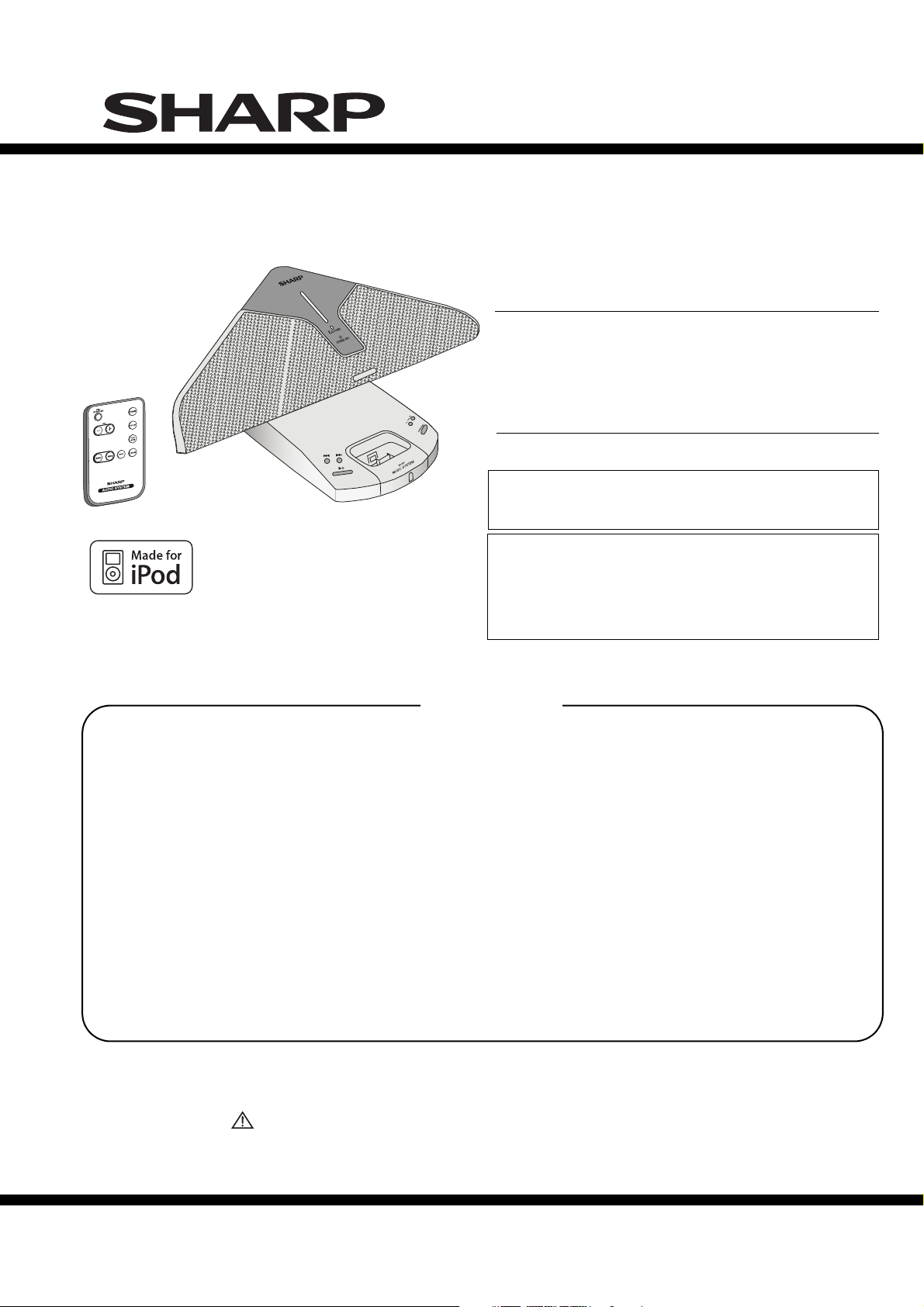
MUSIC SYSTEM FOR iPod
iPod is a trademark of Apple Inc.,
registered in the U.S and other countries
CONTENTS
MODEL
DK-AP2
(For Europe, U.K.)
MUSIC SYSTEM FOR iPod
MODEL
• In the interests of user-safety the set should be restored to
its original condition and only parts identical to those
specified be used.
• Note for users in U.K.
Recording and playback of any material may require
consent which SHARP is unable to give. Please refer
particularly to the provisions of Copyright Act 1956, the
Performers Protection Acts 1963 and 1972 and subsequent
statutory enactments and orders.
DK-AP2(BK
(For Europe, U.K.)
)
PRECAUTIONS FOR USING LEAD-FREE SOLDER
CHAPTER 1. GENERAL DESCRIPTION
[1] Important Service Notes (for U.K. only) ..........1-1
[2] Specifications .................................................1-1
[3] Name Of Parts................................................1-2
CHAPTER 2. MECHANICAL DESCRIPTION
[1] Disassembly .................................................. 2-1
CHAPTER 3. DIAGRAMS
[1] Block Diagram ................................................3-1
CHAPTER 4. CIRCUIT DESCRIPTION
[1] Voltage .......................................................... 4-1
Parts marked with " " are important for maintaining the safety of the set. Be sure to replace these parts with
specified ones for maintaining the safety and performance of the set.
CHAPTER 5. CIRCUIT SCHEMATICS AND PARTS
LAYOUT
[1] Notes On Schematic Diagram .......................5-1
[2] Types Of Transistor And LED........................ 5-1
[3] Chart Of Connecting Wires............................ 5-2
[4] Schematic Diagram .......................................5-4
[5] Wiring Side Of PWB ...................................... 5-14
CHAPTER 6. OTHERS
[1] Function Table Of IC...................................... 6-1
PARTS GUIDE
SHARP CORPORATION
– 1
This document has been published to be used for
after sales service only.
The contents are subject to change without notice.
Page 2
DK-AP2/DK-AP2(BK)
PRECAUTIONS FOR USING LEAD-FREE SOLDER
1. Employing lead-free solder
"MAIN, iPOD, POWER SWITCH, PLAY SWITCH, BATTERY POSITIVE, BATTERY NEGATIVE, LED PWB" of this
model employs lead-free solder. The LF symbol indicates lead-free solder, and is attached on the PWB and
service manuals. The alphabetical character following LF shows the type of lead-free solder.
Example:
Indicates lead-free solder of tin, silver and copper.
2.
Using lead-free wire solder
When fixing the PWB soldered with the lead-free solder, apply lead-free wire solder. Repairing with conventional
lead wire solder may cause damage or accident due to cracks.
As the melting point of lead-free solder (Sn-Ag-Cu) is higher than the lead wire solder by 40°C, we recommend
you to use a dedicated soldering bit, if you are not familiar with how to obtain lead-free wire solder or soldering
bit, contact our service station or service branch in your area.
3.
Soldering
As the melting point of lead-free solder (Sn-Ag-Cu) is about 220°C which is higher than the conventional lead
solder by 40°C,and as it has poor solder wet ability, you may be apt to keep the soldering bit in contact with the
PWB for extended period of time. However, since the land may be peeled of for the maximum heat-resistance
temperature of parts may be exceeded, remove the bit from the PWB as soon as you confirm the steady
soldering condition.
Lead-free solder contains more tin, and the end of the soldering bit may be easily corrected. Make sure to turn
on and off the power of the bit as required. If a different type of solder stays on the tip of the soldering bit, it is
alloyed with lead-free solder. Clean the bit after every use of it.
When the tip of the soldering bit is blackened during use, file it with steel wool or fine sand paper.
Be careful when replacing parts with polarity indication on the PWB silk.
Lead-free wire solder for servicing
Ref No.
PWB-A 92LPWB6822MANS
PWB-B 92LPWB6822SWHS
Parts No.
92LPWB6758LEDSPWB-C
Description
MAIN (A1), iPOD (A2)
POWER SWITCH (B1), PLAY SWITCH (B2), BATTERY POSITIVE (B3),
BATTERY NEGATIVE (B4)
LED
– 2
i
Page 3
DK-AP2/DK-AP2(BK)
CHAPTER 1.
GENERAL DESCRIPTION
CAUTION: “Danger of explosion if battery is incorrectly replaced. Replace only with the same
or equivalent type”.
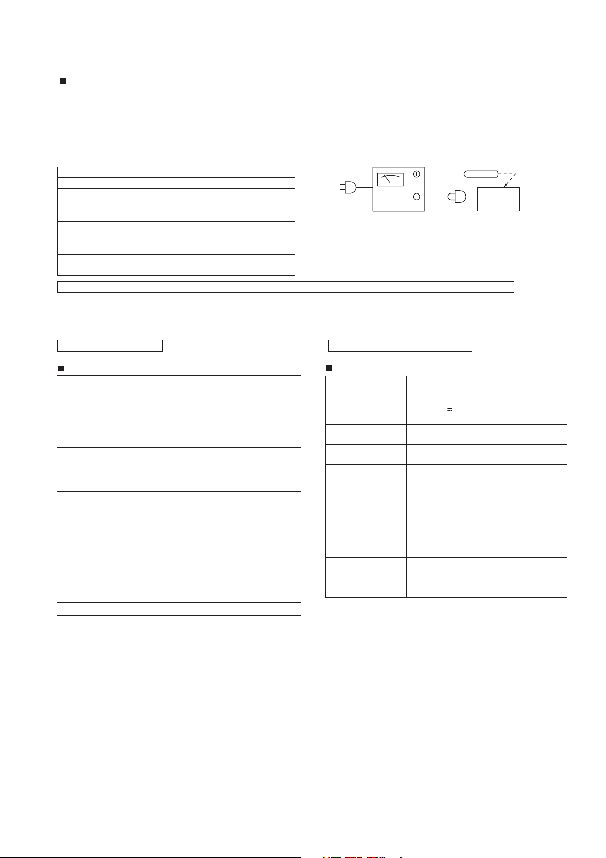
[1] Important Service Notes (for U.K. only)
Before returning the unit to the customer after completion of a repair or adjustment it is necessary for the following withstand voltage test to be
applied to ensure the unit is safe for the customer to use.
Setting of Withstanding Voltage Tester and set.
Set name set value
Withstanding Voltage Tester
Test voltage 4,240 VPEAK
Set time 6 secs
Set current (Cutoff current) 4 mA
Unit
Judgment
OK: The “GOOD” lamp lights.
NG: The “NG” lamp lights and the buzzer sounds.
FOR A COMPLETE DESCRIPTION OF THE OPERATION OF THIS UNIT, PLEASE REFER TO THE OPERATION MANUAL.
[2]
Specifications
3,000 VRMS
DK-AP2/DK-AP2(BK)
DK-AP2/DK-AP2(BK) for U.K.
WITHSTANDING
VOLTAGE TESTER
AC
SHORT-CIRCUIT
AC POWER
SUPPLY CORD
PROBE
OUT
AC/DC
ADAPTOR
CONNECT THE PROBE
TO SHELL OF DC CONNECTOR
General
Power source DC IN 6V 2A: AC/DC adaptor
Power
consumption
Output power Speakers:
Speaker 1-way type speaker system
Speaker maximum
input power
Speaker rated
input power
Output terminals
Input terminals
Dimensions Width: 380 mm (15")
Weight 1.2 kg (2.65 lbs)
*This power consumption value is obtained when in the power
*stand-by mode.
(AC 100 - 240 V ~ 50/60 Hz)
DC IN 3V [ “AA” size (UM/SUM-3, R6 or
HP-7) battery x 4]
Power on : 3.8 W
Power stand-by: 0.2 W (*)
RMS: 3.8 W (1.9 W + 1.9 W) (DIN 45 324)
Speakers: 5 cm (2") - 6 ohms - Full Range
3.8 W/Channel
1.9 W/Channel
Video output: 1Vp-p
Auxiliary (audio signal):
500 mV/47 k ohms
Height: 157 mm (6-2/5")
Depth: 221 mm (8-7/10")
General
Power source
Power
consumption
Output power
Speaker
Speaker maximum
input power
Speaker rated
input power
Output terminals Video output: 1Vp-p
Input terminals Auxiliary (audio signal):
Dimensions Width: 380 mm (15")
Weight 1.2 kg (2.65 lbs)
* This power consumption value is obtained when in the power
stand-by mode.
DC IN 6V 2A: AC/DC adaptor
(AC 100 - 240 V ~ 50/60 Hz)
DC IN 3V [ “AA” size (UM/SUM-3, R6 or
HP-7) battery x 4]
Power on : 3.8 W
Power stand-by: 0.2 W*
Speakers:
RMS: 3.8 W (1.9 W + 1.9 W) (10% T.H.D.)
1-way type speaker system
Speakers: 5 cm (2") - 6 ohms - Full Range
3.8 W/Channel
1.9 W/Channel
500 mV/47 k ohms
Height: 157 mm (6-2/5")
Depth: 221 mm (8-7/10")
1 – 3
1 – 1
Page 4
DK-AP2/DK-AP2(BK)
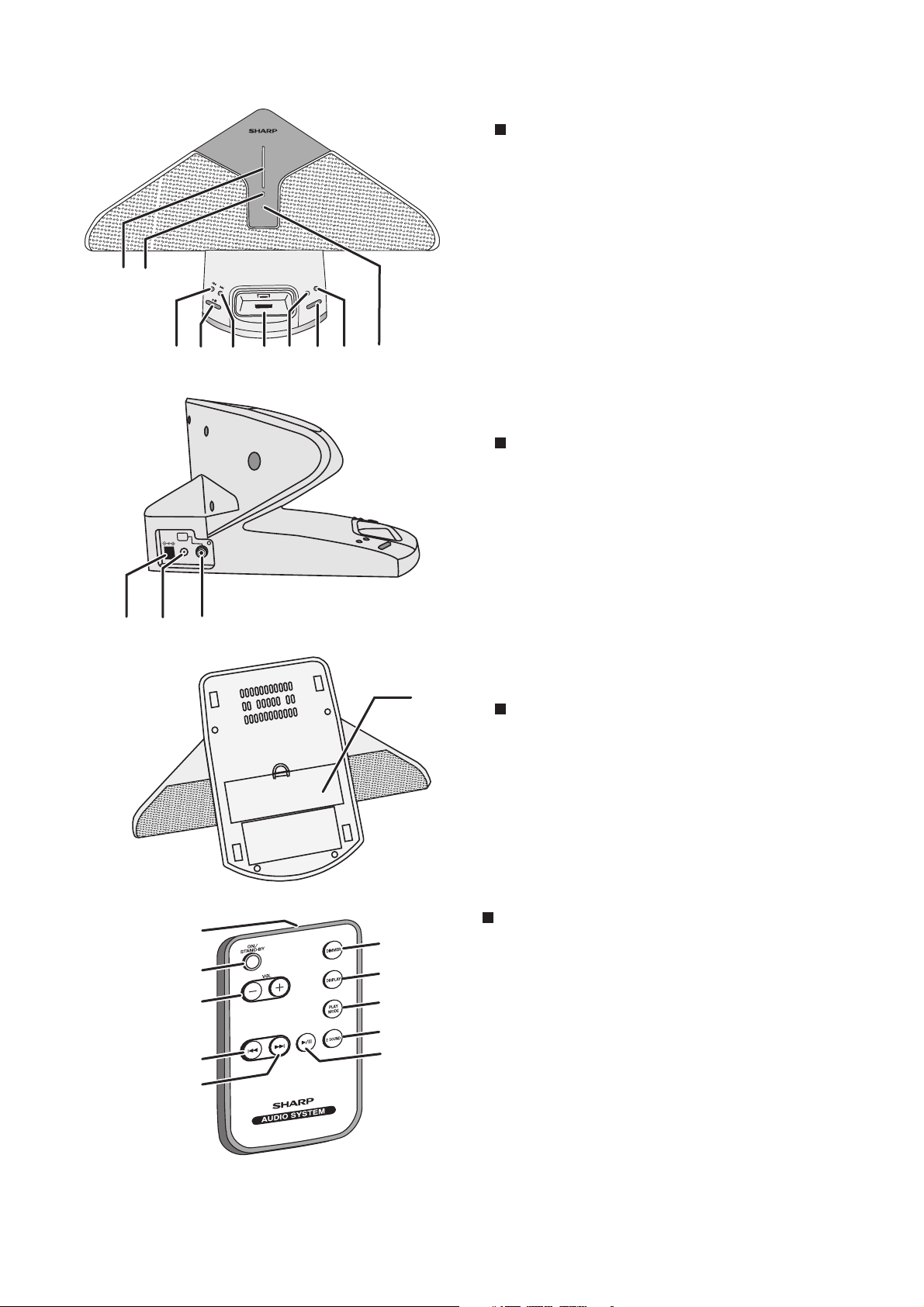
[3] Names Of Parts
12
12
34 5 6 7 8 9
34 5 6 7 8 9
M
M
ESOUND
ESOUND
STAND-BY
STAND-BY
U
U
Top view
1. Power Indicator
2. E SOUND Indicator
3. Skip Down Button
4. Play/Pause Button
5. Skip Up Button
6. iPod Dock
+
+
- VOL
- VOL
-BY
-BY
N/STAND
N/STAND
O
O
P
P
2
2
-
-
K
K
D
D
A
A
M
M
E
E
T
T
S
S
Y
Y
I
I
C
C
S
S
S
S
-
-
-
-
10
10
7. Volume Down Button
8. ON/STAND-BY Button
9. Volume Up Button
10. Stand-by Indicator
Side view
1. DC Input Socket
2. Auxiliary Input Socket
3. Video Out Socket
VIDEO
OUT
DC IN 6V
AUX IN
2
1
3
1
Bottom view
1. Battery Compartment
Remote control
1
2
3
4
5
6
7
8
9
10
1. Remote Control Transmitter
2. On/Stand-by Button
3. Volume Up and Down Buttons
4. Skip Down Button
5. Skip Up Button
6. Dimmer Button
7. Display Button
8. Play Mode Button
9. E SOUND Button
10. Play/Pause Button
1 – 4
1 – 2
Page 5
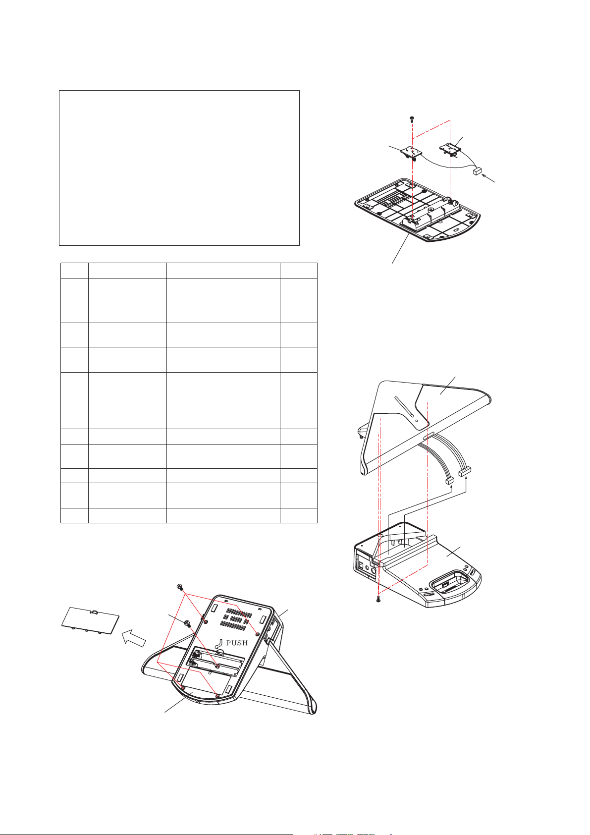
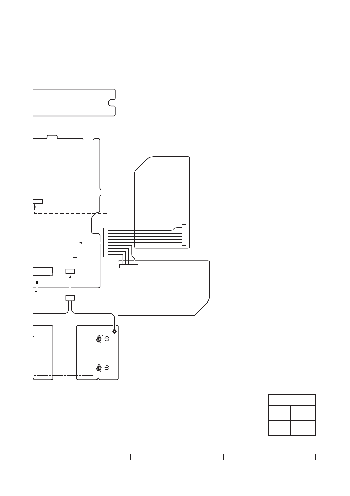
CHAPTER 2. MECHANICAL DESCRIPTION
[1] Disassembly
DK-AP2/DK-AP2(BK)
Caution on disassembly
Follow the below-mentioned notes when disassembling
the unit and reassembling it, to keep it safe and ensure
excellent performance:
1) Be sure to remove the power supply plug from the
wall outlet before starting to disassemble the unit.
2) Take off nylon bands or wire holders where they
need to be removed when disassembling the unit.
After servicing the unit, be sure to rearrange the
leads where they were before disassembling.
3) Take sufficient care on static electricity of integrated
circuits and other circuits when servicing.
STEP REMOVAL PROCEDURE FIGURE
1 Bottom Cover 1
2 Battery Positive PWB/
Battery Negative PWB
3 Speaker Box Ass’y 3
4 Main PWB 4
5 iPOD PWB 5
6 Play Switch PWB/
Power Switch PWB
7 Back Cabinet 6
8 LED PWB 7
9 Speaker 8
1. Open Battery Cover................A1
2. Screw ............................(A2) X 4
3. Screw ............................(A3) X 1
4. Socket ...........................(A4) X 1
1. Screw ............................(B1) X 2
1. Screw ............................(C1) X 3
2. Socket ...........................(C2) X 2
1. Screw ............................(D1) X 1
2. Screw ............................(D2) X 4
3. Screw ............................(D3) X 1
4. Socket ...........................(D4) X 1
5. Flat Cable ...................... (D5) X 1
1. Screw ............................(E1) X 3
1. Screw ............................(F1) X 4
1. Screw ..........................(G1) X 10
1. Screw ............................(H1) X 1
2. Screw ............................(H2) X 2
1. Screw ............................(K1) X 8
2
5
Battery
Negative PWB
Bottom Cover
(B1)x2
M2.6x6mm
Figure 2
Battery
Positive PWB
Speaker Box Ass’y
(C2)x2
From
Main PWB
(A4)x1
From
Main PWB
A1
Battery Cover
(A2)x4
M3x8mm
(A3)x1
M3x8mm
Bottom Cover
Figure 1
Main Unit
2 – 1
(C1)x3
M3x10mm
Bottom Cabinet
Figure 3
Page 6

DK-AP2/DK-AP2(BK)
(D1)x1
M3x8mm
Bottom Cabinet
(H1)x1
M3x10mm
LED PWB
LED Holder
Main PWB
Main Chassis
(D2)x4
M3x10mm
(D3)x1
M3x8mm
Figure 4
Bottom Cabinet
(D5)x1
From Switch PWB
(D4)x1
From iPOD PWB
To
Battery PWB
(H2)x2
M3x10mm
(K1)x4
M3x8mm
Speaker
Speaker Wire
BLUE
(K1)x4
M3x8mm
Front Panel Ass’y
Figure 7
Speaker
RED
Front Panel Ass’y
iPOD PWB
Play Switch PWB
(G1)x10
M3x10mm
(F1)x2
M2.6x8mm
Figure 5
Figure 6
(F1)x2
M2.6x8mm
(E1)x2
M2.6x8mm
Speaker Box Ass’y
Power Switch PWB
Figure 8
Back Cabinet
2 – 2
Page 7

-MEMO-
DK-AP2/DK-AP2(BK)
2 – 3
Page 8

DK-AP2/DK-AP2(BK)
CHAPTER 3. DIAGRAMS
[1] Block Diagram
Figure 1: BLOCK DIAGRAM (1/2)
3 – 1
Page 9
DK-AP2/DK-AP2(BK)
Figure 2: BLOCK DIAGRAM (2/2)
3 – 2
Page 10

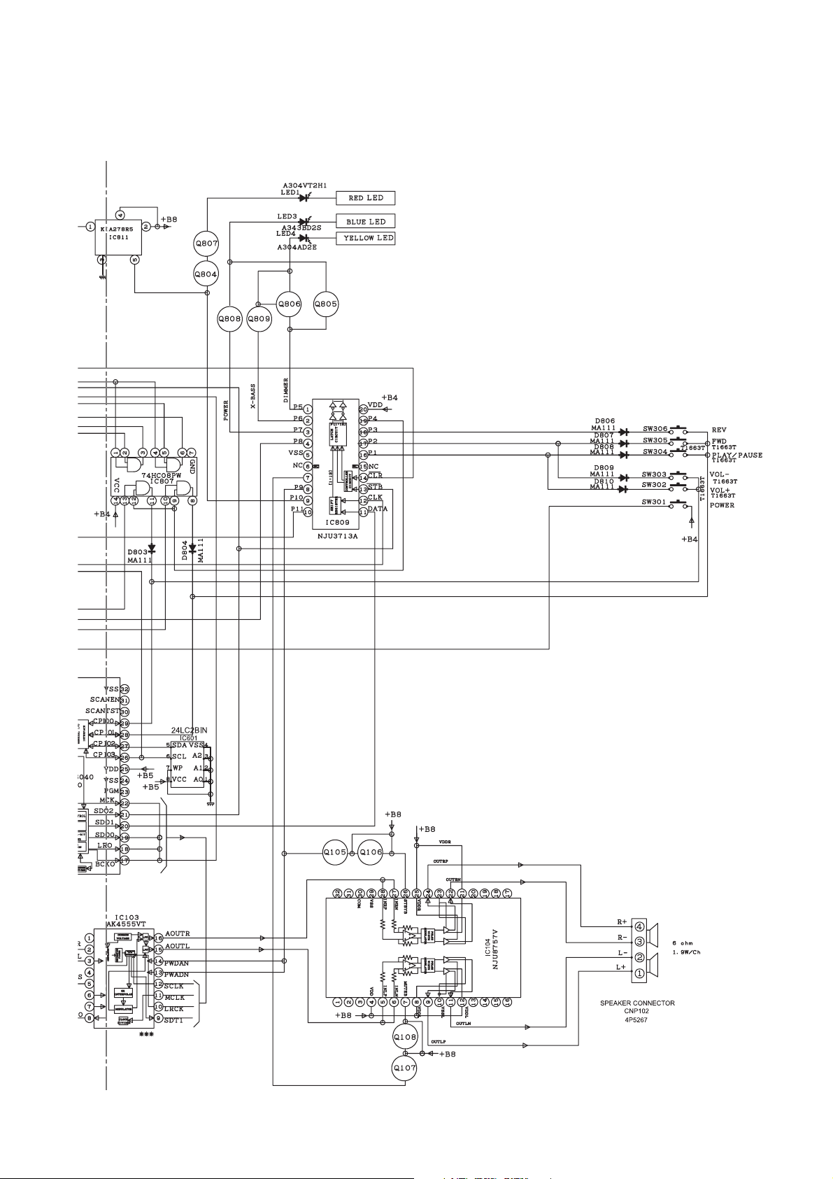
DK-AP2/DK-AP2(BK)
CHAPTER 4.
CIRCUIT DESCRIPTION
[1] Voltage
IC101 IC102 IC103
PINNOVOLTAGE
(V)
1 3.44 1 1.65 1 1.62 9 1.02
2 3.46 2 1.66 2 1.63 10 1.64
3 123.30mV 3 1.65 3 1.64 11 1.62
4 3.46 4 1.90mV 4 2.10mV 12 1.63
5 3.45 5 1.65 5 3.30 13 3.29
6 3.47 6 1.66 6 3.30 14
7 4.93 7 1.65 7 2.10mV 15
8 3.43 8 3.30 8 1.03 16 1.64
9 2.11
10 3.47
IC104
PINNOVOLTAGE
(V)
1 77.10mV 17 200.40mV 1 3.29 17 1.63
2 138.20mV 18 350.20mV 2 3.29 18 -200.80mV
3 4.98 19 46.50mV 3 3.29 19 -166.40mV
4 4.98 20 94.50mV 4 0.20mV 20 185.50mV
5 2.46 21 4.98 5
6 2.42 22 2.48 6 3.27 22
7 3.29 23 -80.30mV 7 -8.60mV 23 0.10mV
8 4.98 24 4.96 8 3.29 24 0.00
9 2.48 25 4.98 9 0.20mV 25 3.29
10 0.50mV 26 3.29 10 1.57 26 1.65
11 20.50mV 27 2.42 11
12 4.98 28 2.46 12 1.40mV 28 0.88
13 0.80mV 29 0.60mV 13 -3.20mV 29 0.50mV
14 7.20mV 30 2.47 14 1.03 30 0.20mV
15 10.50mV 31 -10.70mV 15 -0.30mV 31 0.00
16 12.40mV 32 -24.30mV 16 -0.40mV 32 0.10mV
PINNOVOLTAGE
(V)
PINNOVOLTAGE
(V)
PINNOVOLTAGE
(V)
PINNOVOLTAGE
(V)
3.29
1.53
PINNOVOLTAGE
IC600
PINNOVOLTAGE
21 2.46
27 3.04
(V)
3.29
1.64
(V)
1.62
IC801 IC802
PINNOVOLTAGE
(V)
1 3.29 1 3.29 1 3.29 1 1.35
2 -1.40mV 2 -0.10mV 2 -0.80mV 2 527.00mV
3 2.47 3 1.25 3 1.26 3 1.94
4 3.26 4 3.30 4 3.29 4 -1.10mV
5 5.91 5 5.92 5 5.92 5 5.91
IC805 IC806 IC807
PINNOVOLTAGE
(V)
1 -1.00mV 1 3.29 1 3.26
2 -1.10mV 2 -0.10mV 2 3.24
3 3.27 3 -0.30mV 3 3.29
4 3.29 4 3.29 4 3.26
5 3.29 5 -0.80mV 5 3.29
PINNOVOLTAGE
(V)
PINNOVOLTAGE
(V)
6 3.29 6 3.29
7 -0.80mV 7 -1.10mV
8 2.06 8 0.81
9 1.24 9 0.82
10 3.29 10 3.26
11 1.63 11 -1.00mV
12 2.06 12 0.82
13 2.46 13 7.40mV
14 3.29 14 3.29
IC803
PINNOVOLTAGE
(V)
PINNOVOLTAGE
(V)
IC804
PINNOVOLTAGE
(V)
6
72.22
85.89
1.23
4 – 1
Page 11
DK-AP2/DK-AP2(BK)
IC809 IC810
PIN
VOLTAGE
NO
1 0.60mV 11 0.21 1 2.29 9 2.28
2 -0.30mV 12 1.22 2 2.28 10 3.50mV
3 3.29 13 2.46 3 0.10mV 11 3.50mV
4 3.29 14 3.29 4 0.10mV 12 83.30mV
5 -0.40mV 15 100.20mV 5 0.10mV 13 5.01
6 25.50mV 16 0.82 6 78.50mV 14 5.01
7 3.29 17 0.82 7 3.50mV 15 5.01
8 3.29 18 0.82 8 3.50mV 16 188.80mV
9 3.29 19 0.82
10 -0.20mV 20 3.29
PINNOVOLTAGE
1 5.92 1 6.21
2 4.98 2 0.00
3 0.20mV 3 5.01
4 4.98
5 2.98
(V)
IC811 IC813
(V)
PINNOVOLTAGE
(V)
PINNOVOLTAGE
(V)
PIN
NO
VOLTAGE
(V)
PINNOVOLTAGE
(V)
4 – 2
Page 12

DK-AP2/DK-AP2(BK)
-MEMO-
4 – 3
Page 13
DK-AP2/DK-AP2(BK)
CHAPTER 5. CIRCUIT SCHEMATICS AND PARTS LAYOUT
[1] Notes On Schematic Diagram
• Resistor:
To differentiate the units of resistors, such symbol as
K and M are used: the symbol K means 1000 ohm
and the symbol M means 1000 kohm and the resistor without any symbol is ohm-type resistor.
Besides, the one with “Fusible” is a fuse type.
• Capacitor:
To indicate the unit of capacitor, a symbol P is used:
this symbol P means pico-farad and the unit of the
capacitor without such a symbol is microfarad. As to
electrolytic capacitor, the expression “capacitance/
withstand voltage” is used.
(CH), (TH), (RH), (UJ): Temperature compensation
(ML): Mylar type
(P.P.): Polypropylene type
• Schematic diagram and Wiring Side of P.W.Board
for this model are subject to change for
improvement without prior notice.
REF. NO DESCRIPTION POSITION
SW301 POWER ON / STAND-BY ON—OFF
SW302 VOLUME UP ON—OFF
SW303 VOLUME DOWN ON—OFF
SW304 PLAY/PAUSE ON—OFF
SW305 FORWARD ON—OFF
SW306 REVERSE ON—OFF
• The indicated voltage in each section is the one
measured by Digital Multimeter between such a
section and the chassis with no signal given.
1. In the tuner section,
indicates FM stereo
• Parts marked with “ ” ( ) are
important for maintaining the safety of the set. Be
sure to replace these parts with specified ones for
maintaining the safety and performance of the set.
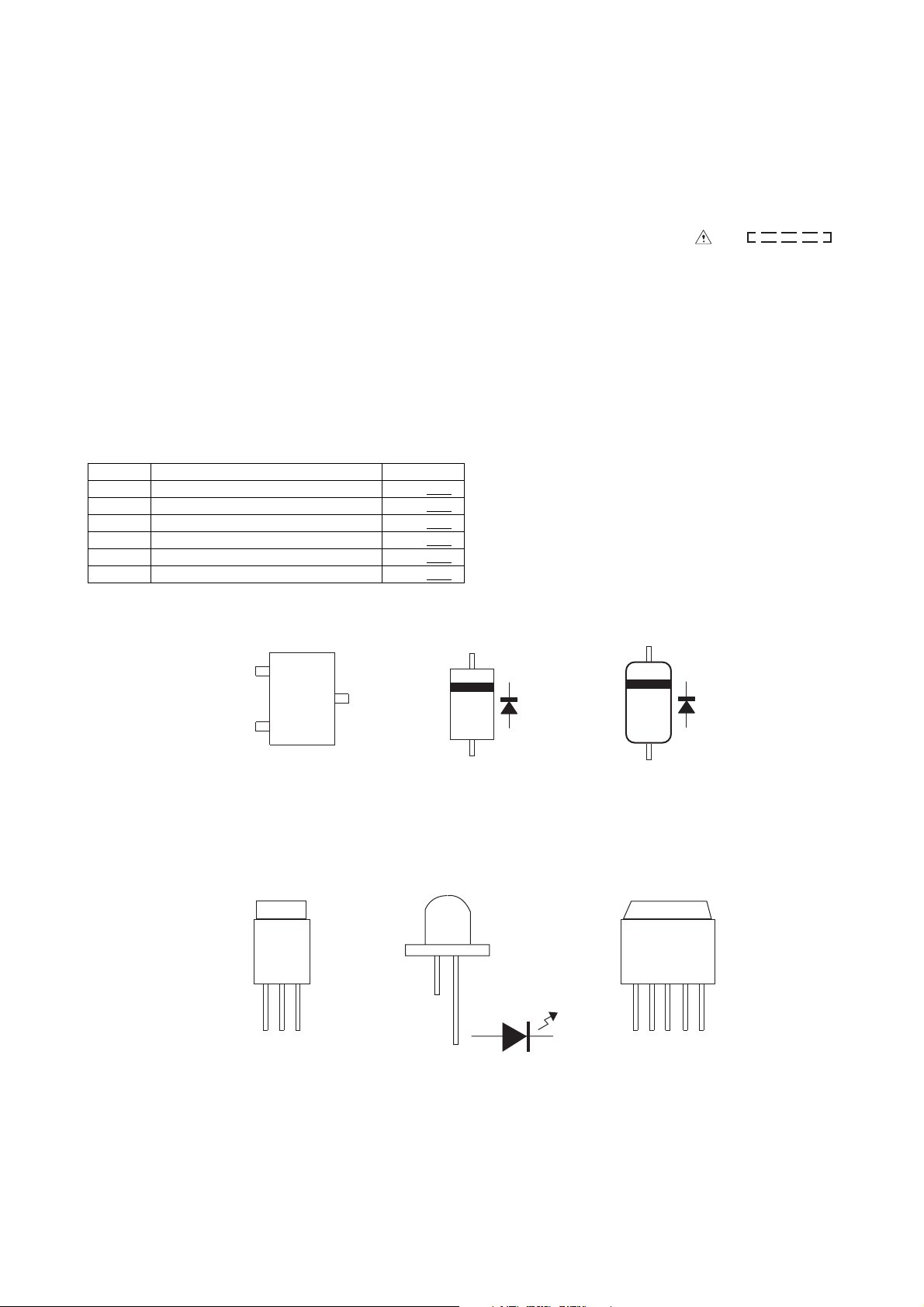
[2] Types Of Transistor And LED
B
(3)
TOP
VIEW
E
(1)
KRC107S
KTC3875 GR
KRA102S
KTC2875B
FRONT
VIEW
3 2 1
KIA78D05
C
(2)
Cathode
Anode
A304VT2H
A343BD2S2
A304AD2E
TOP VIEW
MA111
IN5820
SK24A
MA21038
RB160M30
D1SS119
KiA278R05
FRONT
VIEW
12345
1 - INPUT (Vin)
2 - OUTPUT (V
O)
3 - GND
4 - V
O SENSE
5 - ON/OFF CTRL (V
C)
5 – 1
Page 14
DK-AP2/DK-AP2(BK)
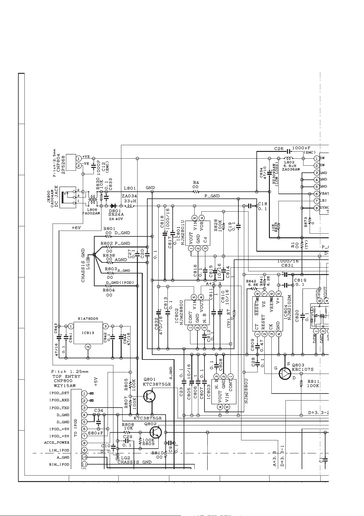
[3] Schematic Diagram
A
B
C
D
E
F
G
H
1
23456
Figure 5-1: MAIN SCHEMATIC DIAGRAM (1/6)
5 – 2
Page 15
DK-AP2/DK-AP2(BK)
7
8 9 10 11 12
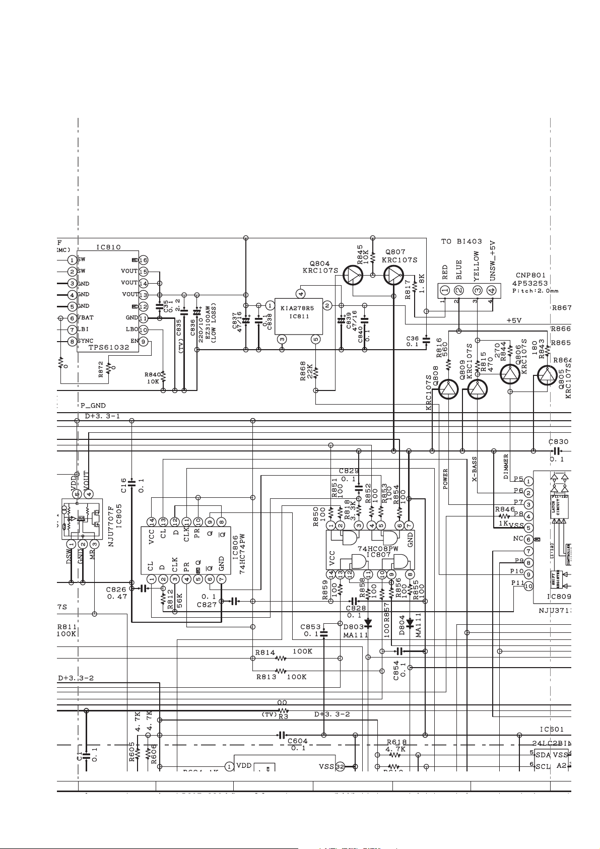
Figure 5-2: MAIN SCHEMATIC DIAGRAM (2/6)
5 – 3
Page 16
DK-AP2/DK-AP2(BK)
13
14 15 16 17 18
Figure 5-3: MAIN SCHEMATIC DIAGRAM (3/6)
5 – 4
Page 17
DK-AP2/DK-AP2(BK)
A
B
C
D
E
F
G
H
1
23456
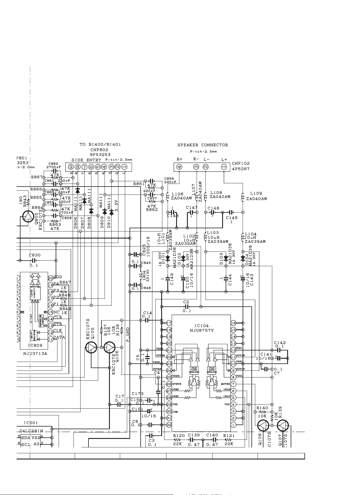
Figure 5-4: MAIN SCHEMATIC DIAGRAM (4/6)
5 – 5
Page 18

DK-AP2/DK-AP2(BK)
7
8 9 10 11 12
Figure 5-5: MAIN SCHEMATIC DIAGRAM (5/6)
5 – 6
Page 19

DK-AP2/DK-AP2(BK)
13
14 15 16 17 18
Figure 5-6: MAIN SCHEMATIC DIAGRAM (6/6)
5 – 7
Page 20

DK-AP2/DK-AP2(BK)
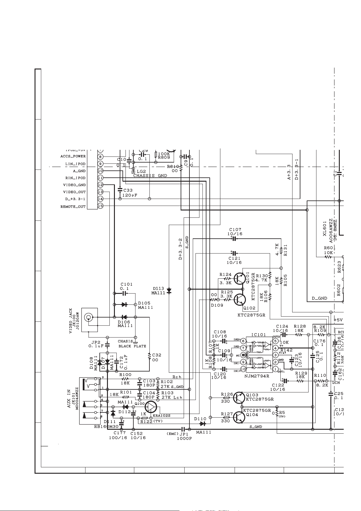
Figure 5-7: IPOD SCHEMATIC DIAGRAM (1/2)
5 – 8
Page 21

DK-AP2/DK-AP2(BK)
Figure 5-8: IPOD SCHEMATIC DIAGRAM (2/2)
5 – 9
Page 22

DK-AP2/DK-AP2(BK)
SCHEMATIC DIAGRAM FOR LED SECTION
SCHEMATIC DIAGRAM FOR SWITCH SECTION
SCHEMATIC DIAGRAM FOR BATTERY SECTION
Figure 5-9: LED, BATTERY AND SWITCH SCHEMATIC DIAGRAM
5 – 10
Page 23

-MEMO-
DK-AP2/DK-AP2(BK)
5 – 11
Page 24

DK-AP2/DK-AP2(BK)
3
2
8
V
[4] Wiring Connection
A
B
LED PWB-C
MAIN PWB-A1
CNS301
1234
RDBKGY
5
BI301
BK
321
4
DC IN 6V
JK800
AUX IN
C
VIDEO OUT
D
E
RD
4
BK
321
BK
BL
CNS102
JK101
JK100
15
FFC202
CNP102
4321
1
15
CNP801
4321
CNP
5791113
468101214
F
G
iPOD PWB-A2
CNP201
CNP202
13579111315
2468101214
RD
BATTERY POSITI
PWB-B3
FROM
H
EXTERNAL IPOD
DEVICE
1
23456
Figure 5-10: WIRING CONNECTION (1/2)
5 – 12
Page 25
C
POWER SWITCH PWB-B1
DK-AP2/DK-AP2(BK)
NP801
21
BI400
RD
123456789
BK
GY
BK
GY
RD
BK
GY
BK
CNS802
12345
BI401
CNP804
21
123456789
CNP802
CNP800
1357911
246810
1
2
3
54
6
2 CNS8041
RD
BL
PLAY SWITCH PWB-B2
BATTERY 1.5V
BATTERY 1.5V
BL
SITIVE
3
BATTERY NEGATIVE
PWB-B4
7
COLOR TABLE
GY
RD
BK
BL
8 9 10 11 12
Figure 5-11: WIRING CONNECTION (2/2)
5 – 13
GRAY
RED
BLACK
BLUE
Page 26
DK-AP2/DK-AP2(BK)
[5] Wiring Side Of PWB
A
MAIN PWB-A1
B
DC IN 6V
C
D
E
F
AUX IN
VIDEO OUT
4321
4321
G
H
1
23456
Figure 5-12: WIRING SIDE OF MAIN PWB (TOP VIEW) (1/2)
5 – 14
Page 27

DK-AP2/DK-AP2(BK)
432
1
1234567
89
1
2468101214
13579111315
2
Lead-free solder indication
Lead-free solder is used in the MAIN PWB.
Refer to "Precautions for handling lead-free solder" for instructions
and precautions.
7
8 9 10 11 12
Figure 5-13: WIRING SIDE OF MAIN PWB (TOP VIEW) (2/2)
5 – 15
Page 28

DK-AP2/DK-AP2(BK)
A
MAIN PWB-A1
B
C
D
C856
R861
C857
R862
C858
E
F
R863
C859
R864
C860
R865
C861
R866
C862
R867
7
0
8R
G
Lead-free solder indication
Lead-free solder is used in the MAIN PWB.
H
Refer to "Precautions for handling lead-free solder" for instructions
and precautions.
1
23456
Figure 5-14: WIRING SIDE OF MAIN PWB (BOTTOM VIEW) (1/2)
5 – 16
Page 29

DK-AP2/DK-AP2(BK)
7
8 9 10 11 12
Figure 5-15: WIRING SIDE OF MAIN PWB (BOTTOM VIEW) (2/2)
5 – 17
Page 30

DK-AP2/DK-AP2(BK)
A
iPOD PWB-A2
B
C
2
31579113151
4
68102141
D
E
F
G
H
Lead-free solder is used in the iPOD PWB.
Refer to “Precautions for handling lead-free solder” for instructions
and precautions.
1
23456
Figure 5-16: WIRING SIDE OF iPOD PWB (TOP VIEW)
5 – 18
Page 31

A
iPOD PWB-A2
B
C
DK-AP2/DK-AP2(BK)
D
E
F
G
H
Lead-free solder is used in the iPOD PWB.
Refer to “Precautions for handling lead-free solder” for instructions
and precautions.
1
23456
Figure 5-17: WIRING SIDE OF iPOD PWB (BOTTOM VIEW)
5 – 19
Page 32

DK-AP2/DK-AP2(BK)
A
B
C
POWER SWITCH PWB-B1 PLAY SWITCH PWB-B2
123
12 34 56
45
BATTERY POSITIVE PWB-B3 BATTERY NEGATIVE PWB-B4
D
E
LED PWB-C
F
12345
G
Lead-free solder is used in the LED, POWER SWITCH, PLAY SWITCH, BATTERY POSITIVE and BATTERY NEGATIVE PWB.
Refer to “Precautions for handling lead-free solder” for instructions
H
and precautions.
1
Figure 5-18: WIRING SIDE OF LED, POWER SWITCH, PLAY SWITCH, BATTERY POSITIVE and BATTERY NEGATIVE PWB (TOP VIEW)
23456
5 – 20
Page 33

CHAPTER 6. OTHERS
[1] Function Table Of IC
IC101 VHiNJM2794R-1 : GROUND NOISE ISOLATION (NJM2794)
DK-AP2/DK-AP2(BK)
BLOCK DIAGRAM
V+
IN1-
OUT1
IN1+
Vref
IN2+
OUT2
IN2-
GND
PIN DESCRIPTION
110
56
No.
1
2
3
4
5
6
7
8
9
10
Symbol Function
OUT1
GND Ground
Vref Reference Voltage
V+ Power Supply
OUT2 Output2
IN2+ +Input2
IN2- -Input2
NC No Connect
IN1- -Input1
IN1+ +Input1
Output1
6 – 1
Page 34

DK-AP2/DK-AP2(BK)
IC102 VHiNJM2115V-1 : DUAL OPERATiONAL AMPLiFiER (NJM2115)
PIN COFIGURATION
(TOP VIEW)
1
A
2
3
45
MARK SPECIFICATION
-+
B
-+
8
7
6
PIN FUNCTION
1. A OUTPUT
2. A-INPUT
3. A+INPUT
-
4. V
5. B+ INPUT
6. B- INPUT
7. B OUTPUT
8. V +
2115
1
2 3
JRC
4
1 Device No. (2115)
2 Last Digit Year
3 Lot No.
4 Manufacturer’s Symbol (JRC)
6 – 2
Page 35

IC600 VHiNJU26040-1 : DiGiTAL SOUND PROCESSOR ( NJU26040 ) ( 1 / 2 )
BLOCK DIAGRAM
DK-AP2/DK-AP2(BK)
SCL/SCK
SDA/SDOUT
RESETb
MCK
CLKOUT
CLK
AD1/SDIN
SERIAL
INTERFACE
TIMING
GENERATOR
HOST
AD2/SSb
24bit Fixed-point DSP Core
PROGRAM
CONTROL
24-BIT x 24-BIT
MULTIPLIER
ALU
ADDRESS GENERATION UNIT
DATA
RAM
FIRMWARE
OTP/RAM
SERIAL AUDIO
INTERFACE
General I/O
INTERFACE
BCK0
LR0
SDO0
SDI
[2:0]
SDO1
SDO2
BCKI
LRI
GPIO3
GPIO2
GPIO1
GPIO0
PIN CONFIGURATION
SDA / SDOUT 2
SCL / SCK 3
AD1 / SDIN 4
AD2 / SSb 5
RESETb 6
CLKOUT 10
VDD 1
VDD 7
VDD 8
VSS 9
CLK 11
SDI2 12
SDI1 13
SDI0 14
LRI 15
BCKI 16
VSS32
TEST31
TEST30
GPIO029
GPIO128
GPIO227
GPIO3 / TEST26
VDD25
VSS24
TEST23
MCK22
SDO221
SDO120
SDO019
LRO18
BCKO17
6 – 3
Page 36

DK-AP2/DK-AP2(BK)
IC2 VHiNJU26040-1: DiGiTAL SOUND PROCESSOR (NJU26040) (2/2)
PIN DESCRIPTION
Pin No. Symbol I/O Description
1, 7, 8, 25 VDD – Power Supply +3.3V
2 SDA / SDOUT OD
3 SCL / SCK I
4 AD1 / SDIN I
5 AD2 / SSb I
6 RESETb I Reset (RESETb=‘Low’ : DSP Reset)
9, 24, 32 VSS – GND
10 CLKOUT O OSC Output
11 CLK I OSC Clock Input
12 SDI2 I Audio Data Input 2
13 SDI1 I Audio Data Input 1
14 SDI0 I Audio Data Input 0
15 LRI I LR Clock Input
16 BCKI I Bit Clock Input
17 BCKO O Bit Clock Output
18 LRO O LR Clock Output
19 SDO0 O Audio Data Output 0
20 SDO1 O Audio Data Output 1
21 SDO2 O Audio Data Output 2
22 MCK O Master Clock Output for A/D, D/A
23, 30, 31 TEST I – for Test (connected to VSS)
26 GPIO3 / TEST I/O + General Purpose IO 3 / for Test (Not connected : OPEN)
27 GPIO2 I/O – General Purpose IO 2
28 GPIO1 I/O – General Purpose IO 1
29 GPIO0 I/O – General Purpose IO 0
I2C I/O / 4-Wire Serial Output
This pin requires a pull-up resistance in both I
2
I
C Clock / Serial Clock
2
C Address / Serial Input
I
2
C Address / Serial Enable
I
2
C bus and 4-Wire serial mode.
6 – 4
Page 37

IC801 VHiNJM2801U-1 : LOW DROPOUT VOLTAGE REGULATOR ( NJM2801U )
PIN CONFIGURATION PIN FUNCTION
5
123
4
V
IN
1.
2.GND
V
3.
OR
C
d
4.
V
OUT
5.
DK-AP2/DK-AP2(BK)
EQUIVALENT CIRCUIT
V
IN
V
OR
GND
V
OUT
Thermal
Protection
+
-
+
-
Cd
Bandgap
Reference
+
-
6 – 5
Page 38

DK-AP2/DK-AP2(BK)
IC802 & IC803 VHiNJM2801U-1 : LOW DROPOUT VOLTAGE REGULATOR ( NJM2880U )
PIN CONFIGURATION PIN FUNCTION
1. CONTROL (Active High)
5
1223
EQUIVALENT CIRCUIT
V
IN
4
2. GND
3. NOISE BYPASS
V
4.
OUT
V
5.
IN
V
OUT
Cont
GND
Bandgap
Reference
Thermal
Protection
Noise Bypass
+
-
6 – 6
Page 39

IC804 VHiNJM2102M-1 : SYSTEM RESET ( NJM2102 )
PIN CONFIGURATION PIN FUNCTION
1. CT
2. RESET
DK-AP2/DK-AP2(BK)
1
2
3
45
BLOCK DIAGRAM
100
kΩ
3. CK
8
7
6
4. GND
+
5. V
V
REF
6.
V
7.
s
8. RESET
+
V
5
+
-
Reference
1.2μA
1.235V1.235V
COMP.O
+
-
10μA
10μA
+
-
6
V
REF
VS
CK
7
40kΩ
3
COMP.S
+
-
Pulse Generator
Q
R
S
Watch
Dog
Timer
CT
281
RESET RESET
4
GND
6 – 7
Page 40

DK-AP2/DK-AP2(BK)
IC805 VHiNJU7707F-1 : VOLTAGE DETECTOR ( NJU7707F )
PIN CONFIGURATION PIN FUNCTION
5
123
EQUIVALENT CIRCUIT
V
DD
4
1. DSW
V
2.
SS
3. MR
V
4.
OUT
V
5.
DD
+
-
Delay Circuit
V
OUT
V
V
V
SS
DD
SS
Vref
Vref
DSW
+
Delay Circuit
-
DSW
MR
MR
V
OUT
6 – 8
Page 41

IC809 VHiNJU3713A-1 : 12-Bit SERIAL TO PARALLEL CONVERTER ( NJU3713A ) (1/2)
PIN CONFIGURATION
V
P5
P6
P7
P8
V
SS
NC
P9
P10
P11
P12
1
2
3
4
5
6
7
8
9
10
20
19
18
17
16
15
14
13
12
11 D ATA
DD
P4
P3
P2
P1
NC
CLR
STB
CLK
DK-AP2/DK-AP2(BK)
BLOCK DIAGRAM
DATA
CLK
STB
CLR
P1
P2
P3
Latch Circuit
Shift Register
P11
P12
Controller Circuit
6 – 9
Page 42

DK-AP2/DK-AP2(BK)
IC809 VHiNJU3713A-1 : 12-Bit SERiAL TO PARALLEL CONVERTER ( NJU3713A ) (2/2)
PIN DESCRIPTION
Pin No. Symbol I/O Description
1P5 O
2P6 O
3P7 O
4P8 O
5V
6 NC – Non Connection
7P9 O
8P10 O
9P11 O
10 PI2 O
11 DATA I Serial Data Input Terminal
12 CLK I Clock Signal Input Terminal
13 STB I Strobe Signal Input Terminal
14 CLR I Clear Signal Input Terminal
15 NC – Non Connection
16 P1 O
17 P2 O
18 P3 O
19 P4 O
20 V
SS
DD
–GND
– Power Supply Terminal (2.4 to 5.5V)
Parallel Conversion Data Output Terminals
Parallel Conversion Data Output Terminals
Parallel Conversion Data Output Terminals
6 – 10
Page 43

IC810 VHiTPS61032-1 : DC - DC CONVERTER ( PS61032 )
BLOCK DIAGRAM
SW
VBAT
Anti-
Ringing
Gate
Control
PGND
DK-AP2/DK-AP2(BK)
VOUT
PGND
PGND
100 kΩ
EN
SYNC
GND
LBI
Regulator
Control Logic
V
REF
GND
Oscillator
Temperature
Low Battery Comparator
= 0.5 V
Error Amplifier
V
Control
REF
10 pF
FB
= 0.5 V
GND
LBO
PIN CONFIGURATION
SW
SW
PGND
PGND
PGND
VBAT
LBI
SYNC
1
2
3
4
5
6
7
8
PowerPAD
16
15
14
13
12
11
10
NC
VOUT
VOUT
VOUT
FB
GND
LBO
9
EN
6 – 11
Page 44

DK-AP2/DK-AP2(BK)
-MEMO-
6 – 12
Page 45

DK-AP2/DK-AP2(BK)
PARTS GUIDE
MUSIC SYSTEM FOR iPod
[1] INTEGRATED CIRCUITS
[2] TRANSISTORS
[3] DIODES
[4] COILS
MODEL
MUSIC SYSTEM FOR iPod
MODEL
CONTENTS
[7] RESISTORS
[8] OTHER CIRCUITRY PARTS
[9] CABINET PARTS
[10] ACCESSORIES/PACKING PARTS
DK-AP2
(For Europe, U.K.)
DK-AP2(BK
(For Europe, U.K.)
)
[5] RESONATOR
[6] CAPACITORS
Parts marked with " " are important for maintaining the safety of the set. Be sure to replace these parts with specified
ones for maintaining the safety and performance of the set.
SHARP CORPORATION
[11] P.W.B. ASSEMBLY (NOT
REPLACEMENT ITEM)
This document has been published to be used
for after sales service only.
0
The contents are subject to change without notice.
Page 46

DK-AP2/DK-AP2(BK)
NO. PARTS CODE
PRICE
RANK
[1] INTEGRATED CIRCUITS
iC101 VHiNJM2794R-1 AN Noise isolation,NJM2794
iC102 VHiNJM2115V-1 AE Low Saturation OP-Amp,NJM2115
iC103 VHiAK4555VT-1 AQ Codec iC
iC104 VHiNJU8757V-1 AT Power Amplifier iC, NJU8757
iC600 VHiNJU26040-1 AX Digital Sound Processor,NJU26040
iC601 VHi24LC2BiN-1 AF 2Kbit EEPROM
iC801 VHiNJM2801U-1 AG Low Dropout Voltage Regulator with Reset,NJM2801
iC802 VHiNJM2880U-1 AG Low Dropout Voltage Regulator ,NJM2880
iC803 VHiNJM2880U-1 AG Low Dropout Voltage Regulator ,NJM2880
iC804 VHiNJM2102M-1 AK System Reset,NJM2102
iC805 VHiNJU7707F-1 AF Voltage Detector,NJU7707
iC806 VHi74HC74PW-1 AE Dual Flip Flop,74HC74PW
iC807 VHi74HC08PW-1 AD Quad and Gate,74HC08PW
iC809 VHiNJU3713A-1 AM 12-BiT Serial to Parallel Coverter
iC810 VHiTPS61032-1 AT DC - DC Converter,PS61032
iC811 VHiKiA278R5-1 AL Voltage Regulator ,5V
iC813 VHiKiA78D05-1 AG Voltage Regulator ,5V
[2] TRANSISTORS
Q100 VSKRA102S//-1 AB Digital,PNP,KRA107 S
Q101 VSKTC2875B/-1 AC Silicon,NPN,KTC2875 B
Q102 VSKTC2875B/-1 AC Silicon,NPN,KTC2875 B
Q103 VSKTC2875B/-1 AC Silicon,NPN,KTC2875 B
Q104 VSKTC2875B/-1 AC Silicon,NPN,KTC2875 B
Q105 VSKRC107S//-1 AB Digital,NPN,KRC107 S
Q106 VSKRC107S//-1 AB Digital,NPN,KRC107 S
Q107 VSKRC107S//-1 AB Digital,NPN,KRC107 S
Q108 VSKRC107S//-1 AB Digital,NPN,KRC107 S
Q601 VSKTC3875GR-1 AB Silicon,NPN,KTC3875 GR
Q801 VSKTC3875GR-1 AB Silicon,NPN,KTC3875 GR
Q802 VSKTC3875GR-1 AB Silicon,NPN,KTC3875 GR
Q803 VSKRC107S//-1 AB Digital,NPN,KRC107 S
Q804 VSKRC107S//-1 AB Digital,NPN,KRC107 S
Q805 VSKRC107S//-1 AB Digital,NPN,KRC107 S
Q806 VSKRC107S//-1 AB Digital,NPN,KRC107 S
Q807 VSKRC107S//-1 AB Digital,NPN,KRC107 S
Q808 VSKRC107S//-1 AB Digital,NPN,KRC107 S
Q809 VSKRC107S//-1 AB Digital,NPN,KRC107 S
[3] DIODES
D101 VHDMA21D38/-1 AC Silicon,MA21D38
D102 VHDMA21D38/-1 AC Silicon,MA21D38
D103 VHDMA21D38/-1 AC Silicon,MA21D38
D104 VHDMA21D38/-1 AC Silicon,MA21D38
D105 VHDMA111///-1 AC Silicon,MA111
D106 VHDMA111///-1 AC Silicon,MA111
D107 VHDMA111///-1 AC Silicon,MA111
D108 VHDMA111///-1 AC Silicon,MA111
D110 VHDMA111///-1 AC Silicon,MA111
D111 VHDRB160M30-1 AC Silicon,RB160M
D112 VHDMA111///-1 AC Silicon,MA111
D113 VHD1SS119//-1 AA Silicon,1SS119
D202 VHDMA111///-1 AC Silicon,MA111
D203 VHDMA111///-1 AC Silicon,MA111
D801 VHDSK24A///-1 AD Silicon,SK24A
D802 VHD1N5820//-1 AD Silicon,1N5820
D803 VHD1N5820//-1 AD Silicon,1N5820 ( SWITCH PWB )
D803 VHDMA111///-1 AC Silicon,MA111 ( MAiN PWB )
D804 VHDMA111///-1 AC Silicon,MA111
D806 VHDMA111///-1 AC Silicon,MA111
D807 VHDMA111///-1 AC Silicon,MA111
D808 VHDMA111///-1 AC Silicon,MA111
D809 VHDMA111///-1 AC Silicon,MA111
D810 VHDMA111///-1 AC Silicon,MA111
LED1 VHP304VT2H1-1 AC LED,Red
LED3 VHPA343BD2S2Z AG LED,Blue
LED4 VHPA304AD2E-1 AD LED,Yellow
[4] COILS
L101 RCILZA039AWZZ AK Coil, 10 µH
L102 RCILZA039AWZZ AK Coil, 10 µH
L103 RCILZA039AWZZ AK Coil, 10 µH
L104 RCILZA039AWZZ AK Coil, 10 µH
L105 RCILZ2130SCT5 AC Coil
L106 RCILZA040AWZZ AD Ferrite Bead,600 ohm
L107 RCILZA040AWZZ AD Ferrite Bead,600 ohm
L108 RCILZA040AWZZ AD Ferrite Bead,600 ohm
L109 RCILZA040AWZZ AD Ferrite Bead,600 ohm
L801 RCILZA034AWZZ AH Inductor, 33 µH
L803 RCILZA036AWZZ AH Inductor, 6.8 µH
L804 RCILZ2130SCT5 AC Coil
L806 RCILFA002AWZZ AL Coil
R612 RCILZA041AWZZ AC Ferrite Bead,120 ohm
R613 RCILZA041AWZZ AC Ferrite Bead,120 ohm
R614 RCILZA041AWZZ AC Ferrite Bead,120 ohm
R615 RCILZA041AWZZ AC Ferrite Bead,120 ohm
R616 RCILZA041AWZZ AC Ferrite Bead,120 ohm
NEW
MARK
PAR T
RANK
DESCRIPTION
1
Page 47

NO. PARTS CODE
PRICE
RANK
NEW
MARK
PAR T
RANK
[4] COILS
R617 RCILZA041AWZZ AC Ferrite Bead,120 ohm
RF1 RCORFA015AWZZ AD Ferrite Core
RF2 RCORFA015AWZZ AD Ferrite Core
[5] RESONATOR
XL601 RCRM-A006AWZZ AE RESONATOR, 36.8MHZ
[6] CAPACITORS
C1 VCKYCY1HB104K AD 0.1 µ F,50V
C2 VCKYCY1HB104K AD 0.1 µ F,50V
C3 VCKYCY1HB104K AD 0.1 µ F,50V
C4 VCKYCY1HB104K AD 0.1 µ F,50V
C5 VCKYCY1HB104K AD 0.1 µ F,50V
C6 VCKYCY1HB104K AD 0.1 µ F,50V
C7 VCKYCY1HB104K AD 0.1 µ F,50V
C8 VCKYCY1HB104K AD 0.1 µ F,50V
C9 VCKYCY1HB104K AD 0.1 µ F,50V
C10 VCKYCY1HB104K AD 0.1 µ F,50V
C11 VCKYCY1HB104K AD 0.1 µ F,50V
C12 VCKYCY1HB102K AA 0.001 µ F,50V
C13 VCKYCY1HB104K AD 0.1 µ F,50V
C14 VCKYCY1HB104K AD 0.1 µ F,50V
C15 VCKYCY1HB104K AD 0.1 µ F,50V
C16 VCKYCY1HB104K AD 0.1 µ F,50V
C17 VCKYCY1HB104K AD 0.1 µ F,50V
C18 VCKYCY1HB104K AD 0.1 µ F,50V
C19 VCKYCY1HB104K AD 0.1 µ F,50V
C20 VCKYCY1HB104K AD 0.1 µ F,50V
C21 VCKYCY1HB104K AD 0.1 µ F,50V
C22 VCKYCY1HB104K AD 0.1 µ F,50V
C23 VCKYCY1HB104K AD 0.1 µ F,50V
C24 VCKYCY1HB104K AD 0.1 µ F,50V
C25 VCKYCY1HB104K AD 0.1 µ F,50V
C26 VCKYCY1HB102K AA 0.001 µ F,50V
C27 VCKYCY1HB104K AD 0.1 µ F,50V
C28 VCKYCY1HB104K AD 0.1 µ F,50V
C29 VCKYCY1HB104K AD 0.1 µ F,50V
C33 VCCCCY1HH121J AA 120 pF (CH),50V
C34 VCCCCY1HH681J AA 680 pF (CH),50V
C35 VCKYCY1HB104K AD 0.1 µ F,50V
C36 VCKYCY1HB104K AD 0.1 µ F,50V
C101 VCKYCY1HB104K AD 0.1 µ F,50V
C103 VCCCCY1HH181J AA 180 pF (CH),50V
C104 VCCCCY1HH181J AA 180 pF (CH),50V
C105 RC-EZD476AF1C AC 47 µ F,16V,Electrolytic
C106 VCKYCY1HB104K AD 0.1 µ F,50V
C107 VCEAZA1CW106M AC 10 µ F,16V,Electrolytic
C108 VCEAZA1CW106M AC 10 µ F,16V,Electrolytic
C109 VCEAZA1CW106M AC 10 µ F,16V,Electrolytic
C120 VCEAZA1CW106M AC 10 µ F,16V,Electrolytic
C121 VCEAZA1CW106M AC 10 µ F,16V,Electrolytic
C122 VCEAZA1CW106M AC 10 µ F,16V,Electrolytic
C123 VCEAZA1CW106M AC 10 µ F,16V,Electrolytic
C124 VCEAZA1CW106M AC 10 µ F,16V,Electrolytic
C125 VCKYCY1HB104K AD 0.1 µ F,50V
C126 VCEAZA1CW106M AC 10 µ F,16V,Electrolytic
C127 VCEAZA1CW106M AC 10 µ F,16V,Electrolytic
C128 VCKYCY1HB104K AD 0.1 µ F,50V
C129 VCEAZA1CW106M AC
C130 VCKYCY1HB104K AD 0.1 µ F,50V
C131 VCEAZA1CW106M AC 10 µ F,16V,Electrolytic
C132 VCEAZA1CW106M AC 10 µ F,16V,Electrolytic
C133 VCEAZA1CW106M AC 10 µ F,16V,Electrolytic
C134 VCKYCY1HB104K AD 0.1 µ F,50V
C135 VCEAZA1CW106M AC 10 µ F,16V,Electrolytic
C136 VCKYCY1HB104K AD 0.1 µ F,50V
C137 VCKYCY1AB474K AC 0.47 µ F,10V
C138 VCKYCY1AB474K AC 0.47 µ F,10V
C139 VCKYCY1AB474K AC 0.47 µ F,10V
C140 VCKYCY1AB474K AC 0.47 µ F,10V
C141 VCEAZA1CW106M AC 10 µ F,16V,Electrolytic
C142 VCKYCY1HB104K AD 0.1 µ F,50V
C143 VCEAZA1CW106M AC 10 µ F,16V,Electrolytic
C144 VCKYCY1EB105K AB 1 µ F,25V
C145 VCKYCY1EB105K AB 1 µ F,25V
C146 VCKYCY1EB105K AB 1 µ F,25V
C147 VCKYCY1EB105K AB 1 µ F,25V
C148 VCKYCY1EB105K AB 1 µ F,25V
C149 VCKYCY1EB105K AB 1 µ F,25V
C150 VCEAZA1CW106M AC 10 µ F,16V,Electrolytic
C151 VCEAZA1CW106M AC 10 µ F,16V,Electrolytic
C152 VCEAZA1CW106M AC 10 µ F,16V,Electrolytic
C162 VCEAZA1HW105M AB 1 µ F,50V,Electrolytic
C163 VCEAZA1HW105M AB 1 µ F,50V,Electrolytic
C164 VCKYCY1HB104K AD 0.1 µ F,50V
C165 VCKYCY1HB104K AD 0.1 µ F,50V
C166 VCKYCY1EF223Z AB 0.022 µ F,25V
C171 VCKYCY1HB104K AD 0.1 µ F,50V
10 µ F,16V,Electrolytic
2
DK-AP2/DK-AP2(BK)
DESCRIPTION
Page 48

DK-AP2/DK-AP2(BK)
NO. PARTS CODE
PRICE
RANK
[6] CAPACITORS
C172 VCKYCY1HB104K AD 0.1 µ F,50V
C177 VCEAZA1CW107M AC 100 µ F,16V,Electrolytic
C201 VCKYCY1HB104K AD 0.1 µ F,50V
C202 VCKYCY1HB104K AD 0.1 µ F,50V
C203 RC-EZD226AF1C AB 22 µ F,25V,Electrolytic
C204 VCKYCY1HB104K AD 0.1 µ F,50V
C205 VCKYCY1HB102K AA 0.001 µ F,50V
C206 VCKYCY1HB102K AA 0.001 µ F,50V
C207 VCCCCY1HH101J AA 100 pF (CH),50V
C208 VCCCCY1HH101J AA 100 pF (CH),50V
C601 VCKYCY1HB104K AD 0.1 µ F,50V
C602 VCKYCY1HB104K AD 0.1 µ F,50V
C603 VCKYCY1HB104K AD 0.1 µ F,50V
C604 VCKYCY1HB104K AD 0.1 µ F,50V
C605 VCCCCY1HH101J AA 100 pF (CH),50V
C606 VCCCCY1HH101J AA 100 pF (CH),50V
C607 VCCCCY1HH101J AA 100 pF (CH),50V
C805 VCEAZA1CW106M AC 10 µ F,16V,Electrolytic
C806 VCKYCY1EB105K AB 1 µ F,25V
C807 VCKYCY1HB104K AD 0.1 µ F,50V
C808 VCKYCY1HB104K AD 0.1 µ F,50V
C809 VCKYCY1AB474K AC 0.47 µ F,10V
C810 VCEAZA1CW106M AC 10 µ F,16V,Electrolytic
C811 VCKYCY1EB105K AB 1 µ F,25V
C812 VCKYCY1HB104K AD 0.1 µ F,50V
C813 VCKYCY1HB104K AD 0.1 µ F,50V
C814 VCKYCY1EB105K AB 1 µ F,25V
C815 VCEAZA1CW106M AC 10 µ F,16V,Electrolytic
C816 VCKYCY1HB104K AD 0.1 µ F,50V
C817 VCKYCY1HB104K AD 0.1 µ F,50V
C818 VCEAZA1CW108M AE 1000 µ F,16V,Electrolytic
C819 VCKYCY1HB104K AD 0.1 µ F,50V
C820 VCKYCY1HB104K AD 0.1 µ F,50V
C825 VCEAZA1CW108M AE 1000 µ F,16V,Electrolytic
C826 VCKYCY1AB474K AC 0.47 µ F,10V
C827 VCKYCY1HB104K AD 0.1 µ F,50V
C828 VCKYCY1HB104K AD 0.1 µ F,50V
C829 VCKYCY1HB104K AD 0.1 µ F,50V
C830 VCKYCY1HB104K AD 0.1 µ F,50V
C831 VCEAZA1CW108M AE 1000 µ F,16V,Electrolytic
C832 VCEAZA1CW477M AC 470 µ F,16V,Electrolytic
C833 VCKYCY1HB104K AD 0.1 µ F,50V
C834 RC-EZ3099AWZZ AE 47 µ F,10V,Electrolytic
C835 VCKYTV1EB225K AB 2.2 µ F,25V
C836 RC-EZ3100AWZZ AE 220 µ F,10V,Electrolytic
C837 VCEAZA1CW476M AB 47 µ F,16V,Electrolytic
C838 VCKYCY1HB104K AD 0.1 µ F,50V
C839 VCEAZA1CW476M AB 47 µ F,16V,Electrolytic
C840 VCKYCY1HB104K AD 0.1 µ F,50V
C841 VCKYCY1HB104K AD 0.1 µ F,50V
C842 VCKYCY1HB104K AD
C843 VCEAZA1CW476M AB 47 µ F,16V,Electrolytic
C844 VCEAZA1CW476M AB 47 µ F,16V,Electrolytic
C845 VCKYCY1HB104K AD 0.1 µ F,50V
C846 VCKYCY1HB104K AD 0.1 µ F,50V
C853 VCKYCY1HB104K AD 0.1 µ F,50V
C854 VCKYCY1HB104K AD 0.1 µ F,50V
C856 VCCCCY1HH221J AA 220 pF (CH),50V
C857 VCCCCY1HH221J AA 220 pF (CH),50V
C858 VCKYCY1HB272K AA 0.0027 µ F,50V
C859 VCCCCY1HH221J AA 220 pF (CH),50V
C860 VCCCCY1HH221J AA 220 pF (CH),50V
C861 VCCCCY1HH221J AA 220 pF (CH),50V
C862 VCKYCY1HB272K AA 0.0027 µ F,50V
JP1 VCKYCY1HB102K AA 0.001 µ F,50V
JP2 VCKYCY1HB104K AD 0.1 µ F,50V
[7] RESISTORS
C32 VRS-CY1JB000J AA 0 ohms,Jumper,0.8x1.55mm
D109 VRS-CY1JB000J AA 0 ohms,Jumper,0.8x1.55mm
D201 VRS-CY1JB000J AA 0 ohms,Jumper,0.8x1.55mm
L201 VRS-CY1JB000J AA 0 ohms,Jumper,0.8x1.55mm
R1 VRS-TV2AB000J AA 0 ohms,Jumper,1.25x2mm
R3 VRS-TV2AB000J AA 0 ohms,Jumper,1.25x2mm
R4 VRS-CY1JB000J AA 0 ohms,Jumper,0.8x1.55mm
R5 VRS-TV2AB000J AA 0 ohms,Jumper,1.25x2mm
R7 VRS-TV2AB000J AA 0 ohms,Jumper,1.25x2mm
R8 VRS-TV2AB000J AA 0 ohms,Jumper,1.25x2mm
R100 VRS-CY1JB183J AA 18 kohms,1/16W
R101 VRS-CY1JB183J AA 18 kohms,1/16W
R102 VRS-CY1JB273J AA 27 kohms,1/16W
R103 VRS-CY1JB273J AA 27 kohms,1/16W
R104 VRS-CY1JB470J AA 47 ohms,1/16W
R105 VRS-CY1JB183J AA 18 kohms,1/16W
R106 VRS-CY1JB183J AA 18 kohms,1/16W
R107 VRS-CY1JB102J AA 1 kohms,1/16W
R108 VRS-CY1JB102J AA 1 kohms,1/16W
R109 VRS-CY1JB822J AA 8.2 kohms,1/16W
NEW
MARK
PAR T
RANK
0.1 µ F,50V
3
DESCRIPTION
Page 49

NO. PARTS CODE
PRICE
RANK
NEW
MARK
PAR T
RANK
[7] RESISTORS
R110 VRS-CY1JB822J AA 8.2 kohms,1/16W
R111 VRS-CY1JB393J AA 39 kohms,1/16W
R112 VRS-CY1JB393J AA 39 kohms,1/16W
R113 VRS-CY1JB563J AA 56 kohms,1/16W
R114 VRS-CY1JB563J AA 56 kohms,1/16W
R115 VRS-CY1JB221J AA 220 ohms,1/16W
R116 VRS-CY1JB221J AA 220 ohms,1/16W
R117 VRS-CY1JB100J AA 10 ohms,1/16W
R118 VRS-CY1JB223J AA 22 kohms,1/16W
R119 VRS-CY1JB223J AA 22 kohms,1/16W
R120 VRS-CY1JB223J AA 22 kohms,1/16W
R121 VRS-CY1JB223J AA 22 kohms,1/16W
R122 VRS-TV2AB102J AA 1 kohms,1/10W
R124 VRS-CY1JB332J AA 3.3 kohms,1/16W
R125 VRS-CY1JB332J AA 3.3 kohms,1/16W
R126 VRS-CY1JB332J AA 3.3 kohms,1/16W
R127 VRS-CY1JB332J AA 3.3 kohms,1/16W
R128 VRS-CY1JB183J AA 18 kohms,1/16W
R129 VRS-CY1JB183J AA 18 kohms,1/16W
R130 VRS-CY1JB472J AA 4.7 kohms,1/16W
R131 VRS-CY1JB472J AA 4.7 kohms,1/16W
R132 VRS-CY1JB221J AA 220 ohms,1/16W
R137 VRS-CY1JB103J AA 10 kohms,1/16W
R138 VRS-CY1JB103J AA 10 kohms,1/16W
R139 VRS-CY1JB103J AA 10 kohms,1/16W
R140 VRS-CY1JB103J AA 10 kohms,1/16W
R201 VRS-CY1JB562D AA 5.6 kohms,1/16W
R202 VRS-CY1JB274D AA 270 kohms,1/16W
R203 VRS-CY1JB274D AA 270 kohms,1/16W
R204 VRS-CY1JB000J AA 0 ohms,Jumper,0.8x1.55mm
R205 VRS-CY1JB102J AA 1 kohms,1/16W
R206 VRS-CY1JB102J AA 1 kohms,1/16W
R207 VRS-CY1JB104J AA 100 kohms,1/16W
R208 VRS-CY1JB104J AA 100 kohms,1/16W
R209 VRS-CY1JB101J AA 100 ohms,1/16W
R210 VRS-CY1JB101J AA 100 ohms,1/16W
R211 VRS-CY1JB104D AA 100 kohms,1/16W
R212 VRS-CY1JB104D AA 100 kohms,1/16W
R214 VRS-CY1JB154D AA 150 kohms,1/16W
R215 VRS-CY1JB154D AA 150 kohms,1/16W
R217 VRS-CY1JB104D AA 100 kohms,1/16W
R218 VRS-CY1JB104D AA 100 kohms,1/16W
R223 VRS-CY1JB101J AA 100 ohms,1/16W
R224 VRS-CY1JB154D AA 150 kohms,1/16W
R225 VRS-CY1JB154D AA 150 kohms,1/16W
R601 VRS-CY1JB103J AA 10 kohms,1/16W
R602 VRS-CY1JB104J AA 100 kohms,1/16W
R603 VRS-CY1JB330J AA 33 ohms,1/16W
R604 VRS-CY1JB105J AA 1 Mohms,1/16W
R605 VRS-CY1JB472J AA 4.7 kohms,1/16W
R606 VRS-CY1JB472J AA
R607 VRS-CY1JB221J AA 220 ohms,1/16W
R608 VRS-CY1JB221J AA 220 ohms,1/16W
R609 VRS-CY1JB221J AA 220 ohms,1/16W
R610 VRS-CY1JB221J AA 220 ohms,1/16W
R611 VRS-CY1JB221J AA 220 ohms,1/16W
R618 VRS-CY1JB472J AA 4.7 kohms,1/16W
R619 VRS-CY1JB472J AA 4.7 kohms,1/16W
R620 VRS-CY1JB104J AA 100 kohms,1/16W
R621 VRS-CY1JB104J AA 100 kohms,1/16W
R622 VRS-CY1JB104J AA 100 kohms,1/16W
R623 VRS-CY1JB104J AA 100 kohms,1/16W
R624 VRS-CY1JB102J AA 1 kohms,1/16W
R625 VRS-CY1JB102J AA 1 kohms,1/16W
R626 VRS-CY1JB102J AA 1 kohms,1/16W
R627 VRS-CY1JB102J AA 1 kohms,1/16W
R628 VRS-CY1JB102J AA 1 kohms,1/16W
R629 VRS-CY1JB102J AA 1 kohms,1/16W
R630 VRS-CY1JB102J AA 1 kohms,1/16W
R631 VRS-CY1JB102J AA 1 kohms,1/16W
R801 VRS-CY1JB000J AA 0 ohms,Jumper,0.8x1.55mm
R802 VRS-CY1JB000J AA 0 ohms,Jumper,0.8x1.55mm
R803 VRS-CY1JB000J AA 0 ohms,Jumper,0.8x1.55mm
R804 VRS-CY1JB000J AA 0 ohms,Jumper,0.8x1.55mm
R805 VRS-CY1JB104J AA 100 kohms,1/16W
R807 VRS-CY1JB104J AA 100 kohms,1/16W
R808 VRS-CY1JB103J AA 10 kohms,1/16W
R809 VRS-CY1JB104J AA 100 kohms,1/16W
R810 VRS-CY1JB000J AA 0 ohms,Jumper,0.8x1.55mm
R811 VRS-CY1JB104J AA 100 kohms,1/16W
R812 VRS-CY1JB563J AA 56 kohms,1/16W
R813 VRS-CY1JB102J AA 1 kohm,1/16W
R814 VRS-CY1JB104J AA 100 kohms,1/16W
R815 VRS-CY1JB471J AA 470 ohms,1/16W
R816 VRS-CY1JB561J AA 560 ohms,1/16W
R817 VRS-CY1JB182J AA 1.8 kohm,1/16W
R818 VRS-CY1JB332J AA 3.3 kohm,1/16W
R828 VRS-CY1JB104J AA 100 kohms,1/16W
R830 VRS-CY1JB103J AA 10 kohms,1/16W
4.7 kohms,1/16W
4
DK-AP2/DK-AP2(BK)
DESCRIPTION
Page 50

DK-AP2/DK-AP2(BK)
NO. PARTS CODE
PRICE
RANK
[7] RESISTORS
R835 VRS-CY1JB103J AA 10 kohms,1/16W
R838 VRS-CY1JB000J AA 0 ohms,Jumper,0.8x1.55mm
R840 VRS-CY1JB103J AA 10 kohms,1/16W
R841 VRS-CY1JB822J AA 8.2 kohm,1/16W
R842 VRS-CY1JB682J AA 6.8 kohm,1/16W
R843 VRS-CY1JB181J AA 180 ohms,1/16W
R844 VRS-CY1JB271J AA 270 ohms,1/16W
R845 VRS-CY1JB103J AA 10 kohms,1/16W
R846 VRS-CY1JB102J AA 1 kohm,1/16W
R847 VRS-CY1JB102J AA 1 kohm,1/16W
R848 VRS-CY1JB102J AA 1 kohm,1/16W
R849 VRS-CY1JB102J AA 1 kohm,1/16W
R850 VRS-CY1JB101J AA 100 ohms,1/16W
R851 VRS-CY1JB101J AA 100 ohms,1/16W
R852 VRS-CY1JB101J AA 100 ohms,1/16W
R853 VRS-CY1JB101J AA 100 ohms,1/16W
R854 VRS-CY1JB101J AA 100 ohms,1/16W
R855 VRS-CY1JB101J AA 100 ohms,1/16W
R856 VRS-CY1JB101J AA 100 ohms,1/16W
R857 VRS-CY1JB101J AA 100 ohms,1/16W
R858 VRS-CY1JB101J AA 100 ohms,1/16W
R859 VRS-CY1JB101J AA 100 ohms,1/16W
R861 VRS-CY1JB473J AA 47 kohms,1/16W
R862 VRS-CY1JB473J AA 47 kohms,1/16W
R863 VRS-CY1JB473J AA 47 kohms,1/16W
R864 VRS-CY1JB473J AA 47 kohms,1/16W
R865 VRS-CY1JB473J AA 47 kohms,1/16W
R866 VRS-CY1JB473J AA 47 kohms,1/16W
R867 VRS-CY1JB473J AA 47 kohms,1/16W
R868 VRS-CY1JB223J AA 22 kohms,1/16W
R872 VRS-CY1JB000J AA 0 ohms,Jumper,0.8x1.55mm
R873 VRS-CY1JB000J AA 0 ohms,Jumper,0.8x1.55mm
[8] OTHER CIRCUITRY PARTS
Bi301 QCNWNA832AWPZ AH Connector Ass'y,5 / 4 Pin with CNS301
CNP102 92LCONE4P5267 AB Plug,4 Pin
CNP201 QCNCWA046AW30 AQ Socket,30Pin
CNP202 QCNCWZY15AWZZ AD Socket,15Pin
CNP800 QCNCWZX15AWZZ AD Socket,15 Pin
CNP801 92LCONE4P53253 AB Plug,4 Pin
CNP802 92LCONE9P53253 AC Plug,9 Pin
CNP804 92LCONE2P5268 AE Plug,2 Pin
CNS802 QCNWNA837AWPZ AK Connector Ass'y,4 / 5 ~ 9Pin with Bi400 / Bi401
CNS804 QCNWNA836AWPZ AE Connector Ass'y,2Pin
FFC202 QCNWNA840AWPZ AF FFC Cable, 15 Pin
JK100 QSOCJ0120AWZZ AD Audio Jack
JK101 QJAKM0004AWZZ AK Headphone Jack
JK800 QJAKCA004AWZZ AD Power Jack
LG1 QLUGP0001AWZZ AC Lug Terminal
RX100 VHLKSM603SM-1 AG Remote Sensor
SW301 92LSWICHT1663T AC Switch,Key Type [Power On/Standby]
SW302 92LSWICHT1663T AC Switch,Key Type [Volume Up]
SW303 92LSWICHT1663T AC Switch,Key Type [Volume Down]
SW304 92LSWICHT1663T AC Switch,Key Type [Play/Pause]
SW305 92LSWICHT1663T AC Switch,Key Type [Forward]
SW306 92LSWICHT1663T AC Switch,Key Type [Reverse]
NEW
MARK
PAR T
RANK
DESCRIPTION
5
Page 51

[9] CABINET PARTS
606x10
DK-AP2/DK-AP2(BK)
207
232
227X2
604X2
PWB-C
603X3
212
604
213
226
220X2
219
206
211X2
607X4
228
607X4
BLUE
603X3
SP1
202
RED
201
231
205
226
220X2
SP2
201-1
201-2
201-3
233
PWB-A1
605
604X4
601X2
PWB-B3
214
210
230
604X3
605
217X4
218
608
209
PWB-B2
204
602X2
208
PWB-B1
602X2
PWB-A2
602X3
602X2
PWB-B4
215
203
609X4
229
216
6
Page 52

DK-AP2/DK-AP2(BK)
NO. PARTS CODE
PRICE
RANK
[9] CABINET PARTS
201 CPNLSA069AW02 BB Front Panel Ass'y [ DK-AP2 ]
201 CPNLSA069AW03 BB Front Panel Ass'y [ DK-AP2(BK) ]
201-1 ------------- --- Front Panel [ DK-AP2 ] (Not Replacement item)
201-1 ------------- --- Front Panel [ DK-AP2(BK) ] (Not Replacement item)
201-2 ------------- --- Grill, Punching [ DK-AP2 ] (Not Replacement item)
201-2 ------------- --- Grill, Punching [ DK-AP2(BK) ] (Not Replacement item)
201-3 PCUSGA112AWSA AC Cushion, Speaker
202 GCABAA075AWSA AW Cabinet, Bottom [ DK-AP2 ]
202 GCABAA075AWSB AV Cabinet, Bottom [ DK-AP2(BK) ]
203 GCOVAA173AWSA AP Cover, Bottom [ DK-AP2 ]
203 GCOVAA173AWSB AN Cover, Bottom [ DK-AP2(BK) ]
204 HDECQA366AWSA AF Cover, Remote Control
205 HDECQA381AW01 AQ Panel, Decoration
206 HINDPA004AWSA AG Reflector
207 HPNLSA068AWSA AX Cabinet, Back [ DK-AP2(BK) ]
207 HPNLSA068AWSB AY Cabinet, Back [ DK-AP2 ]
208 JKNBZA229AWSA AM Button, Power
209 JKNBZA230AWSA AM Button, Play/Pause
210 LCHSMA069AWFW AK Chassis, Main
211 LHLDZA047AWZZ AC Holder, LED
212 LHLDZA064AWZZ AC Holder, LED
213 LHLDZA172AWZZ AG Holder, Edge Light
214 MSPRDA038AWFW AB Spring, A
215 MSPRDA039AWFW AC Spring, B
216 PCOVQA015AWSA AG Cover, Battery [ DK-AP2(BK) ]
216 PCOVQA015AWSB AG Cover, Battery [ DK-AP2 ]
217 PCUSGA110AWZZ AB Cushion, Leg
218 PCUSSA052AWZZ AD Cushion, Battery
219 PCUSSA055AWZZ AE Cushion, Wire
220 PCUSSA056AWZZ AE Cushion, Duct Port [ DK-AP2(BK) ]
220 PCUSSA066AWZZ AE Cushion, Duct Port [ DK-AP2 ]
226 PDUC-A063AWSA AL Port, Flare [ DK-AP2(BK) ]
226 PDUC-A063AWSB AG Port, Flare [ DK-AP2 ]
227 PFILSA001AWZZ AP Module, T.B.I.
228 QCNWNA833AWPZ AK Wire, Speaker
229 TSPC-A816AWZZ AC Label, Specification [ DK-AP2 ] [For Europe]
229 TSPC-A817AWZZ AC Label, Specification [ DK-AP2(BK) ] [For Europe]
229 TSPC-A818AWZZ AC Label, Specification [ DK-AP2 ] [For U.K.]
229 TSPC-A819AWZZ AC Label, Specification [ DK-AP2(BK) ] [For U.K.]
230 92LNBAND1318A AA Nylon Band, 80mm
231 PCUSSA053AWZZ Cushion, Back Cabinet, A
232 PCUSSA054AWZZ Cushion, Back Cabinet, B
233 PCUSSA038AWZZ AB Cushion
SP 1,2 RSP-ZA245AWZZ BA Speaker
601 XEBY726P06000 AA Screw, M2.6 X 6mm
602 XEBY726P08000 AA Screw, M2.6 X 8mm
603 XEBY730P08000 AA Screw, M3 X 8mm
604 XEBY730P10000 AA Screw, M3 X 10mm
605 XEBY830P08000 AB Screw, M3 X 8mm
606 XEBY830P10000 AB Screw, M3 X 10mm
607 XESY730P08000 AB
608 XJBY730P08000 AA Screw, M3 X 8mm
609 XJSY830P10000 AB Screw, M3 X 10mm
NEW
MARK
PAR T
RANK
DESCRIPTION
Screw, M3 X 8mm
7
Page 53

[10] ACCESSORIES / PACKING PARTS
PACKING METHOD (FOR U.K. ONLY)
DK-AP2/DK-AP2(BK)
1 AC Power Supply Cord [ DK-AP2(BK) ] QACCBA004AW00
1 AC Power Supply Cord [ DK-AP2 ] QACCBA004AW09
2 AC/DC Adaptor [ DK-AP2(BK) ] RADPAA036AWZZ
2 AC/DC Adaptor [ DK-AP2 ] RADPAA039AWZZ
3 Remote Control [ DK-AP2 ] RRMCGA126AWSA
3 Remote Control [ DK-AP2(BK) ] RRMCGA127AWSA
4 Pulp, Bottom SPAKAA163AWZZ
5 Pulp, Top SPAKAA164AWZZ
6 Packing Case [ DK-AP2 ] SPAKCA487AWZZ
6 Packing Case [ DK-AP2(BK) ] SPAKCA488AWZZ
7 Carton [ DK-AP2 ] SPAKGA095AWZZ
7 Carton [ DK-AP2(BK) ] SPAKGA096AWZZ
1. PACK UNIT TO PACKING CASE
10
18
3
8 Polyethylene Bag, AC Cord SPAKP0026AWZZ
9 Polyethylene Bag, Accessories SSAKAA011AWZZ
10 Miramat Bag, Unit SSAKH0045AWZZ
11 Sheet, Caution TCAUZA077AWZZ
12 Warranty Card TGAN-3170UMZZ
13 Warranty Sheet TGANZA021AW01
14 Operation Manual TINSEA187AWZZ
15 Quick Guide TINSEA197AWZZ
16 Label, Energy (GEA) TLABZA274AWZZ
17 Label, Pop TLABZA567AWZZ
18 Adaptor Accessories [ DK-AP2 ] UACRTA007AW01
18 Adaptor Accessories [ DK-AP2(BK) ] UACRTA008AW01
5
17
MAIN UNIT
16
4
11, 12, 13, 14, 15
9
2. PACK PACKING CASE TO CARTON
Front Side Of Unit
8
1
2
6
Front of Packing Case
Packing Case
TOP
TOP
BACK
7
8
Page 54

DK-AP2/DK-AP2(BK)
NO. PARTS CODE
[10] ACCESSORIES / PACKING PARTS
!
!
!
!
!
!
1 QACCBA004AW00 AU AC Power Supply Cord [ DK-AP2(BK) ] [ For U.K.]
1 QACCBA004AW09 AU AC Power Supply Cord [ DK-AP2 ] [ For U.K.]
1 QACCEA004AW00 AM AC Power Supply Cord [ DK-AP2(BK) ] [ For Europe]
1 QACCEA004AW09 AM AC Power Supply Cord [ DK-AP2 ] [ For Europe]
2 RADPAA036AWZZ BC AC/DC Adaptor [ DK-AP2(BK) ]
2 RADPAA039AWZZ BC AC/DC Adaptor [ DK-AP2 ]
3 RRMCGA126AWSA AX Remote Control [ DK-AP2 ]
3 RRMCGA127AWSA AX Remote Control [ DK-AP2(BK) ]
4 SPAKAA163AWZZ AM Pulp, Bottom
5 SPAKAA164AWZZ AM Pulp, Top
6 SPAKCA487AWZZ AY Packing Case [ DK-AP2 ]
6 SPAKCA488AWZZ AY Packing Case [ DK-AP2(BK) ]
7 SPAKGA095AWZZ AR Carton [ DK-AP2 ]
7 SPAKGA096AWZZ AR Carton [ DK-AP2(BK) ]
8 SPAKP0026AWZZ AB Polyethylene Bag, AC Cord [ For U.K. only ]
9 SSAKAA011AWZZ AB Polyethylene Bag, Accessories
10 SSAKH0045AWZZ AD Miramat Bag, Unit
11 TCAUZA077AWZZ AE Sheet, Caution [ For U.K. ]
11 TCAUZA078AWZZ AE Sheet, Caution [ For Europe ]
12 TGAN-3170UMZZ AE Warranty Card [ For U.K.only ]
13 TGANZA021AW01 AE Warranty Sheet [ For U.K.only ]
14 TINSEA187AWZZ AE Operation Manual [ For U.K.]
14 TINSZA273AWZZ AR Operation Manual [ For Europe ]
15 TINSEA197AWZZ AD Quick Guide [ For U.K.only ]
16 TLABZA274AWZZ AB Label, Energy (GEA)
17 TLABZA567AWZZ AD Label, Pop
18 UACRTA007AW01 AP Adaptor Accessories [ DK-AP2 ]
18 UACRTA008AW01 AP Adaptor Accessories [ DK-AP2(BK) ]
[11] P.W.B. ASSEMBLY (Not Replacement Item)
!
PWB-A 92LPWB6822MANS - Main A1/ iPod A2
PWB-B 92LPWB6822SWHS - Power Switch B1/ Play Switch B2 /Battery Positive B3/ Battery Negative B4
PWB-C 92LPWB6758LEDS - LED
PRICE
RANK
NEW
MARK
PAR T
RANK
DESCRIPTION
9
Page 55

-MEMO-
DK-AP2/DK-AP2(BK)
Page 56

DK-AP2/DK-AP2(BK)
A0708
SG SK
 Loading...