SHARP CD-DH790N Diagram
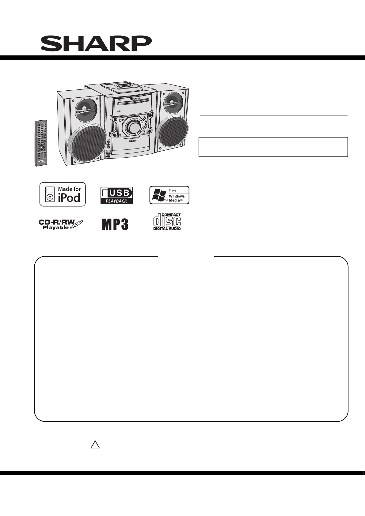
CD-DH790N
SERVICE MANUAL
No. S8938CDDH790N
MINI COMPONENT SYSTEM
M
E
YST
TS
N
E
N
PO
OM
IC
90
IN
7
M
-DH
D
C
N
R
E
W
O
P
Y
B
D-
N
TA
S
/
N
O
CD
B
S
U
E
P
A
T
IN
DIO
AU
NES
PHO
FUNCTIO
VOL
H
PUS
N
E
OP
MODEL
CD-DH790N
CD-DH790N Mini Component System consisting of
CD-DH790N (main unit) and CP-DH790N (speaker system).
• In the interests of user-safety the set shoul d be restored
to its original condition and only parts identical to those
specified be used.
iPod is a trademark of Apple Inc.,
registered in the U.S. and other countries.
“Made for iPod” means that an electronic accessory has
been designed to connect specifically to iPod and has been
certified by the developer to meet Apple performance
standards.
CONTENTS
PRECAUTIONS FOR USING LEAD-FREE SOLDER
CHAPTER 1. GENERAL DESCRIPTION
[1] Important Service Safety Precaution.............. 1-1
[2] Important Service Notes (for U.S.A only).......1-1
[3] Specifications................................................. 1-2
[4] Name Of Parts ............................................... 1-3
CHAPTER 2. ADJUSTMENTS
[1] Mechanism Section........................................ 2-1
CHAPTER 3. MECHANISM BLOCKS
[1] Caution On Disassembly................................ 3-1
CHAPTER 4. DIAGRAMS
[1] Main Block Diagram....................................... 4-1
[2] Servo Block Diagram ....................................4-3
Apple is not responsible for the operation of thi
s device or its
compliance with safety and regulatory standards.
CHAPTER 5. CIRCUIT DESCRIPTION
[1] Waveforms Of CD Circuit ..............................5-1
[2] Voltage...........................................................5-2
CHAPTER 6. CIRCUIT SCHEMATICS AND PARTS
LAYOUT
[1] Notes On Schematic Diagram.......................6-1
[2] Types Of Transistor And LED........................6-1
[3] Schematic Diagram.......................................6-2
[4] Charts Of Connecting Wires .......................6-22
[5] Wiring Side Of PWB....................................6-24
CHAPTER 7. FLOWCHART
[1] Troubleshooting.............................................7-1
CHAPTER 8. OTHERS
[1] Function Table Of IC......................................8-1
[2] FL Display............................. ... ...... .... ... ... ... ...8-9
PARTS GUIDE
Parts marked with " " are important for maintaining the safety of the set. Be sure to replace these parts with
!
specified ones for maintaining the safety and performance of the set.
This document has been published to be used
SHARP CORPORATION
for after sales service only.
The contents are subject to change without notice.
CD-DH790N
PRECAUTIONS FOR USING LEAD-FREE SOLDER
1.Employing lead-free solder
"MAIN, POWER, DISPLAY, SPACER, REGULATOR, TAPE, SERVO, iPod PWB" of this model employs lead-free
solder. The LF symbol indicates lead-free solder, and is attached on the PWB and service manuals. The
alphabetical character following LF shows the type of lead-free solder.
Examples:
Indicates lead-free solder of tin, silver and copper.
2.
Using lead-free wire solder
When fixing the PWB soldered with the lead-free solder, apply lead-free wire solder. Repairing with conventional
lead wire solder may cause damage or accident due to cracks.
As the melting point of lead-free solder (Sn-Ag-Cu) is higher than the lead wire solder by 40°C, we recommend
you to use a dedicated soldering bit, if you are not familiar with how to obtain lead-free wire solder or soldering
bit, contact our service station or service branch in your area.
3.
Soldering
As the melting point of lead-free solder (Sn-Ag-Cu) is about 220°C which is higher than the conventional lead
solder by 40°C,and as it has poor solder wettability, you may be apt to keep the soldering bit in contact with the
PWB for extended period of time. However, since the land may be peeled of for the maximum heat-resistance
temperature of parts may be exceeded, remove the bit from the PWB as soon as you confirm the steady
soldering condition.
Lead-free solder contains more tin, and the end of the soldering bit may be easily corrected. Make sure to turn
on and off the power of the bit as required.
If a different type of solder stays on the tip of the soldering bit, it is alloyed with lead-free solder. Clean the bit
after every use of it.
When the tip of the soldering bit is blackened during use, file it with steel wool or fine sandpaper.
Be careful when replacing parts with polarity indication on the PWB silk.
Lead-free wire solder for servicing
Ref No.
PWB-A 92LPWB7773MANS MAIN (A1), POWER (A2), DISPLAY (A3), SPACER (A4), REGULATOR (A5), TAPE (A6)
PWB-B RUITKA036AWZZ SERVO
PWB-C 92LPWB7119PODS iPod
Parts No.
Description
– i –
CD-DH790N
CHAPTER 1. GENERAL DESCRIPTION
[1] Important Service Safety Precaution
CAUTION : “These servicing instructions are for use by qualified service personnel only. To reduce
the risk of electric shock do not perform any servicing other than that contained in the operating
instructions unless you are qualified to do so”.
WARNING
1. For continued safety, no modification of any circuit should be attempted.
2. Disconnect AC power before servicing.
CAUTION: FOR CONTINUED
PROTECTION AGAINST FIRE
HAZARD, REPLACE ONLY WITH
SAME TYPE F801, F802, F805 5A, 125V/
F80, F804 2.5A, 125V/
F808 1.6A, 125V FUSES.
ATTENTION: POUR ASSURER
UNE LONGUE PROTECTION CONTRE
UN INCENDIE, REMPLACER SEULEMENT
PAR UN FUSIBLE DE
TYPE F801, F802, F805 5A, 125V/
F803, F804 2.5A, 125V/
F808 1.6A, 125V FUSES.
[2] Important Service Notes (for U.S.A only)
BEFORE RETURNING THE AUDIO PRODUCT
(Fire & Shock Hazard)
Before returning the audio product to the user,
perform the following safety checks.
1. Inspect all lead dress to make certain that leads
are not pinched or that hardware is not lodged
between
the chassis and other metal parts in the
audio product.
2. Inspect all protective devices such as insulating
materials, cabinet, terminal board, adjustment and
compartment covers or shields, mechanical
insulators etc.
3. To be sure that no shock hazard exists, check for
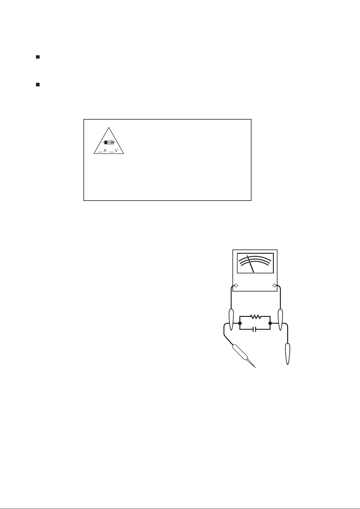
leakage current in the following manner.
Plug the AC line cord directly into a 120 volt AC
*
outlet.
Using two clip leads, connect a 1.5k ohm, 10
*
watt resistor paralleled by a 0.15µF capacitor in
series with all exposed metal cabinet parts and
a known earth ground, such as conduit or
electrical ground connected to earth ground.
Use a VTVM or VOM with 1000 ohm per volt, or
*
higher, sensitivity to measure the AC voltage drop
across the resistor (See diagram).
Connect the resistor connection to all exposed
*
metal parts having a return path to the chassis
(antenna, metal cabinet, screw heads, knobs and
control shafts, escutcheon, etc.) and measure the
AC voltage drop across the resistor.
VTVM
AC SCALE
1.5k ohms
10W
0.15 µ F
TEST PROBE
TO EXPOSED
METAL PARTS
CONNECT TO
KNOWN EARTH
GROUND
All check must be repeated with the AC line cord plug
connection reversed.
Any reading of 0.3 volt RMS (this corresponds to 0.2
milliamp. AC.) Or more is excessive and indicates a
potential shock hazard which must be corrected before
returning the audio product to the owner.
1 – 1
–2
CD-DH790N
[3] Specifications
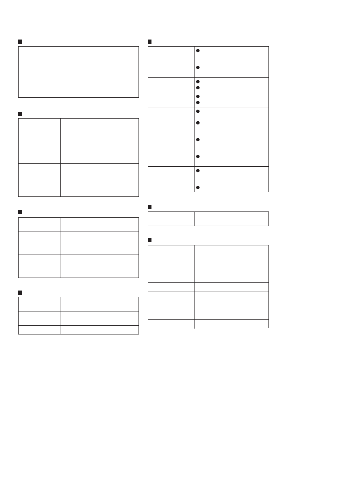
General
Power source AC 120 V ~ 60 Hz
Power
consumption
Dimensions Width: 9 - 7/16" (240 mm)
Weight 8.8 lbs. (5.4 kg)
55 W
Height: 12 - 7/16" (315.5 mm)
Depth: 11 - 5/32" (283.2 mm)
Amplifier
Output power PMPO: 2800 watts
Output terminals Speakers: 4 ohms
Input terminals Audio In (audio signal):
RMS: Total 200 watts
(100 watts per channel into 4
ohms at 1 kHz, 10% total
harmonic distortion)
FTC: 75 watts minimum RMS per
channel into 4 ohms from 100
Hz to 20 kHz, 10% total
harmonic distortion.
Headphones: 16 - 50 ohms
(recommended: 32 ohms)
250 mV/47 k ohms
CD player
Type Single disc multi-play compact disc
Signal readout Non-contact, 3-beam
D/A converter Multi bit D/A converter
Frequency
response
Dynamic range 90 dB (1 kHz)
player
semiconductor laser pickup
20 - 20,000 Hz
Cassette deck
Frequency
response
Signal/noise
ratio
Wow and flutter 0.35% (WRMS)
50 - 14,000 Hz (normal tape)
50 dB (playback)
USB
USB host interface Complies with USB 1.1 (Full
Support file MPEG 1 Layer 3
Bitrate support MP3 (32 ~ 320 kbps)
Other Maximum total number of
File system
support
Speed)/ 2.0 Mass Storage
Class.
Support Bulk only and CBI
protocol.
WMA (Non DRM)
WMA (64 ~ 160 kbps)
MP3/WMA files is 1024.
Maximum total number of
folders is 255 INCLUSIVE of
root directory.
The ID3TAG information
supported are TITLE, ARTIST
and ALBUM only.
Supports ID3TAG version 1
and version 2.
Support USB devices with
Microsoft Windows/DOS/FAT
12/ FAT 16/ FAT 32.
2 kbyte block length for sector.
Tuner
Frequency range FM: 87.5 - 108 MHz
AM: 530 - 1,720 kHz
Speaker
Type 2-way type speaker system
Maximum input
power
Rated input power 100 W
Impedance 4 ohms
Dimensions Width: 7-1/16" (180 mm)
Weight 6.0 lbs. (2.7 kg)/each
2" (5 cm) tweeter
5-1/8" (13 cm) woofer
200 W
Height: 11-13/16" (300 mm)
Depth: 8" (204 mm)
1 – 2
– 4
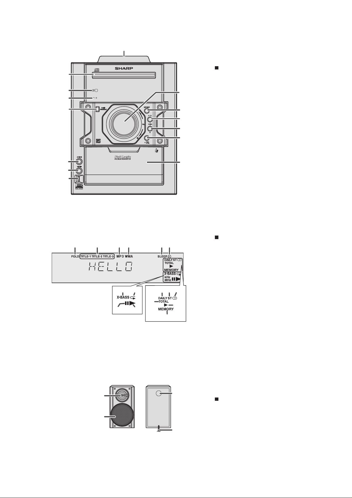
[4] Names Of Parts
2
3
4
5
AUDIO IN
6
PHONES
7
8
MINI COMPONENT SYSTEM
POWER
ON/STAND-BY
CD-DH790
CD-DH790N
1
Front panel
1. iPod Docking Station
2. Disc Tray
3. Remote Sensor
4. Timer Indicator
5. Power On/Stand-by Button
6. Audio In Jack
7. Headphone Jack
8. USB Terminal
9. Volume Control
10. FUNCTION Button
11. Disc / USB / iPod Play or Pause / Tape Play /
Tuning Up Button
12. Disc / USB / Tape Stop / Tuning Down Button
13. Disc Tray Open / Close Button
14. Cassette Compartment
VOL
FUNCTION
9
10
11
12
13
PUSH
OPEN
14
1 2 34 5
13 14
8 9 10
7
15
16
12
1
2
Display
6
11
1. MP3/WMA Folder Indicator
2. MP3/WMA Title Indicators
3. MP3 Indicator
4. WMA Indicator
5. Sleep Indicator
6. Once Timer Play Indicator
7. MP3/WMA Total Indicator
8. Daily Timer Play Indicator
9. FM Stereo Mode Indicator
10. FM Stereo Receiving Indicator
11. Tape play Indicator
12. Memory Indicator
13. Extra Bass Indicator
14. Disc/USB Repeat Play Indicator
15. Disc/USB Pause Indicator
16. Disc/USB Play Indicator
3
Speaker System
1. Tweeter
2. Woofer
3. Bass Reflex Duct
4. Speaker Wire
4
1 – 3
–2
CD-DH790N
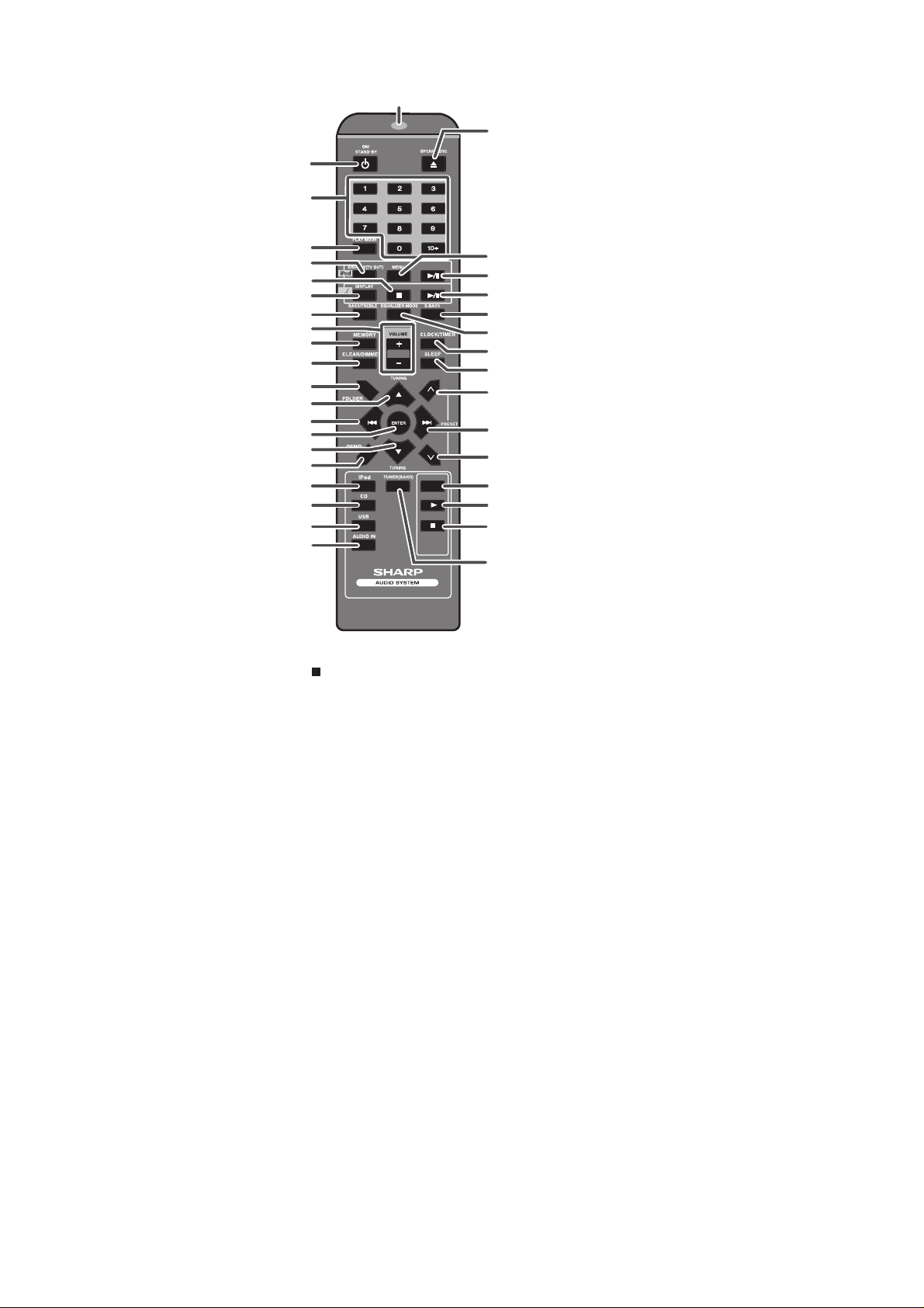
1
22
2
3
4
5
6
7
8
9
10
11
12
CD
USB
23
24
25
26
27
28
29
30
13
14
15
16
17
18
19
20
TAPE
31
32
33
34
35
21
36
Remote control
1. Remote Control Transmitter
2. On/Stand-by Button
3. Direct Search Buttons
4. Play Mode Button
5. iPod Display (TV OUT) Button
6. Disc/USB Stop Button
7. Disc/USB Display Button
8. Bass/Treble Button
9. Volume Up or Down Buttons
10. Memory Button
11. Clear/Dimmer Button
12. Folder Button
13. Tuning Up, iPod Cursor Up Button
14. CD Track Down or Fast Reverse, Time Down Button
15. Enter Button
16. Tuning Down, iPod Cursor Down Button
17. Demo Button
18. iPod Button
19. Disc Button
20. USB Button
21. Audio In Button
22. Open/Close Button
23. iPod Menu Button
24. iPod Play/Pause Button
25. Disc/USB Play/Pause Button
26. X-Bass Button
27. Equaliser Mode Button
28. Clock/Timer Button
29. Sleep Button
30. Tuner Preset Up Button
31. CD Track Up or Fast Forward, Time Up Button
32. Tuner Preset Down Button
33. Tape Button
34. Tape Play Button
35. Tape Stop Button
36. Tuner (Band) Button
1 – 4
– 4
CD-ES700/CD-ES77CD-ES700/CD-ES77Service ManualCD-ES700/CD-ES77MarketE
CHAPTER 2. ADJUSTMENTS
[1] Mechanism Section
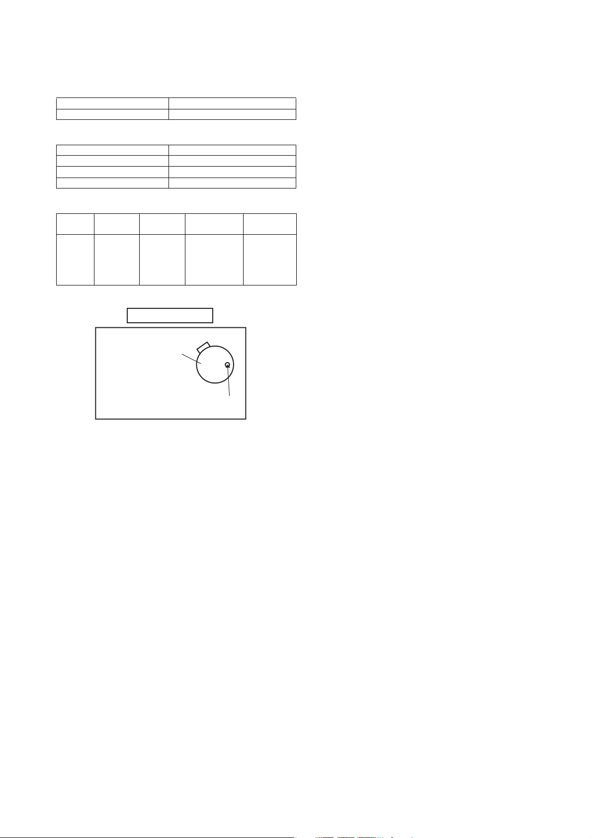
• Driving Force Check
Torque Meter Specified Value
Play: TW-2111 Tape 1: Over 90 g
• Torque Check
Torque Meter Specified Value
Play: TW-2111 29 to 75 g.cm
Fast Forward: TW-2231 55 to 170 g.cm
Rewind: TW-2231 55 to 170 g.cm
• Tape Speed
CD-DH790N
Test Tape Adjusting
Normal
speed
Figure 1
MTT-111 Variable
Point
Resistor in
motor.
TAPE MECHANISM
Tape Motor
Variable Resistor in motor
Specified
Value
3,000 ± 90 Hz
Speaker
Instrument
Connection
Speaker
Terminal
(Load
resistance:
6 ohms)
2 – 1
CD-DH790N
CD-ES700/CD-ES77CD-ES700/CD-ES77Service ManualCD-ES700/CD-ES77MarketE
CHAPTER 3. MECHANISM BLOCKS
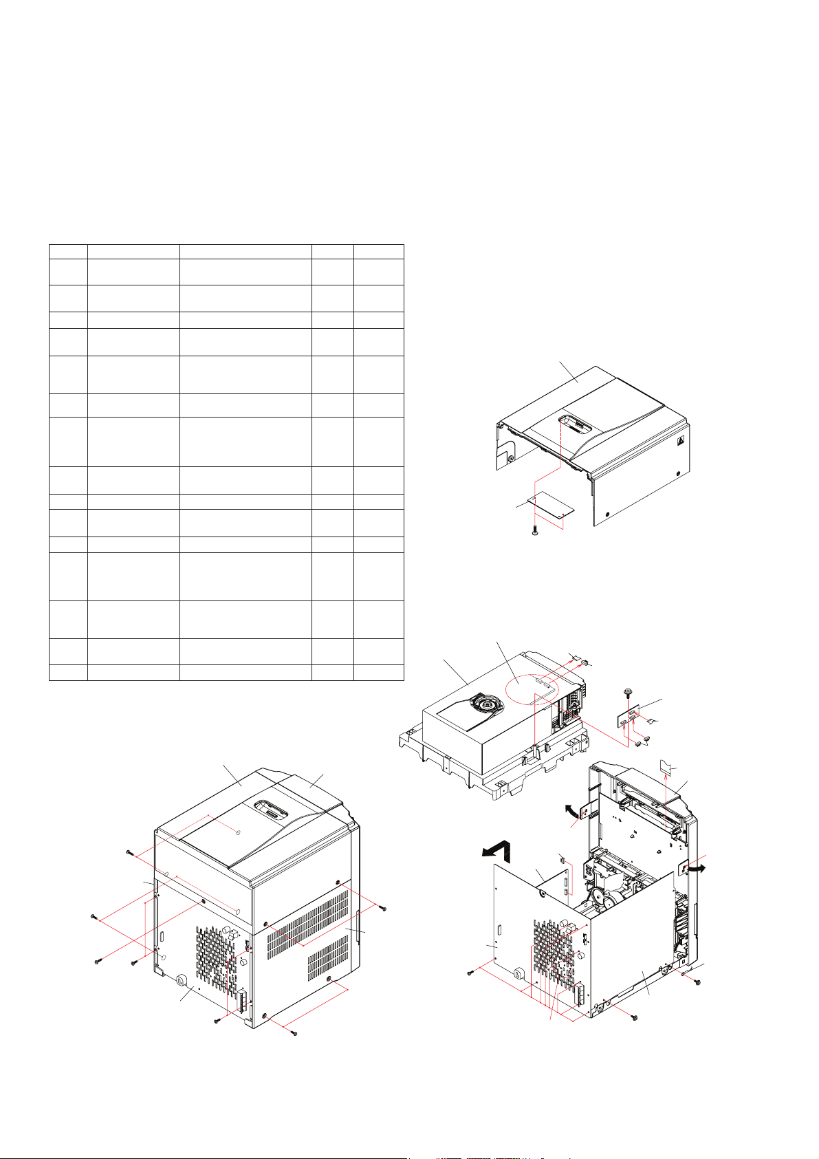
[1] Caution On Disassembly
Follow the below-mentioned notes when disassembling the unit and reassembling it, to keep it safe and ensure
excellent performance:
1. Take cassette tape and compact disc out of the unit.
2. Be sure to remove the power supply plug from th e wall outlet before starting to disassemble the unit.
3. Take off nylon bands or wire holders where they need to be re moved when disassembling th e un it. After servicing
the unit, be sure to rearrange the leads where they were before disassembling.
STEP REMOVAL PROCEDURE FIGURE
.........
(A1)x5
(A2)x1
(B1)x8 1
(C1)x2 2
(D1)x1
(D2)x2
(E1)x2
(E2)x1
(E3)x1
(F1)x9 3
(G1)x2
(G2)x2
(G3)x4
(G4)x2
(H1)x4
(H2)x1
(J4)x4 4
(K1)x6
(K2)x1
(L1)x1 6
(M1)x1
(M2)x1
(M3)x1
(M4)x4
(N1)x2
(N2)x2
(N3)x1
(P1)x4
(P2)x1
(Q1)x4 9
1 Top Cabinet
Side Panel (Left/
2
Right)
iPod PWB
3
4 iPod Transit PWB
5 CD Changer unit
Rear Panel with
6
Fan motor
7 Front Panel
8Main PWB
9Power PWB
10 Tape Mechanism
11 Audio In PWB
12 Display PWB
13 CD PWB
Changer
14
Mechanism Unit
15 CD Mechanism
..........................
1. Screw
2. Flat Cable....................
2. Screw
..........................
..........................
1. Screw
..........................
1. Screw
2. Socket
1. Hook
2. Socket
3. Flat Cable
1. Screw
1. Screw
2. Flat Cable
3. Socket
4. Hook
1. Screw
2. Socket
1. Screw
1. Screw
2. Flat Cable
1. Screw
1. Knob
2. Nut
3. Washer
4. Screw
1. Screw
2. Flat Cable
3. Socket
1. Screw
.........................
...........................
..........................
.....................
...........................
..........................
...................
........................
...........................
..........................
.........................
..........................
..........................
....................
..........................
...........................
..............................
........................
..........................
..........................
....................
.........................
..........................
2. Changer Chassis
1. Screw
..........................
Note:
After removing the connector for the optical pickup from the connector,
wrap the conductive aluminium foil around the front end of the connector
so as to protect the optical pickup from electrostatic damage.
Top Cabinet
Front Panel
4
3,4
3,4
4
3, 4
4
1
3
3
3
5
6
7
8
CD Changer Unit
iPod PWB
M3 x 10mm
CD Servo PWB
Top Cabinet
(C1) x 2
Figure 2
(E3) x 1
(E2) x 1
(D1) x 1
Special Screw
iPod
Transit PWB
(A2) x 1
(D2) x 2
(G2) x 1
Front Panel
(B1) x 2
M3 x 10mm
(A1) x 1
M3 x 12mm
(A1) x 2
M3 x 12mm
Side Panel
(Right)
(B1) x 2
M3 x 10mm
Figure 1
Rear Panel
(B1) x 2
M3 x 10mm
(B1) x 2
M3 x 10mm
(A1) x 2
M3 x 12mm
Side Panel (Left)
3 – 1
Rear Panel
(F1) x 9
M3 x 10mm
PULL
(E1) x 1
(G3) x 1
Power PWB
Fan Motor
Figure 3
Hook
Main PWB
(H1) x 1
Special Screw
Hook
(E1) x 1
PULL
Lug wire
(H1) x 1
Special Screw
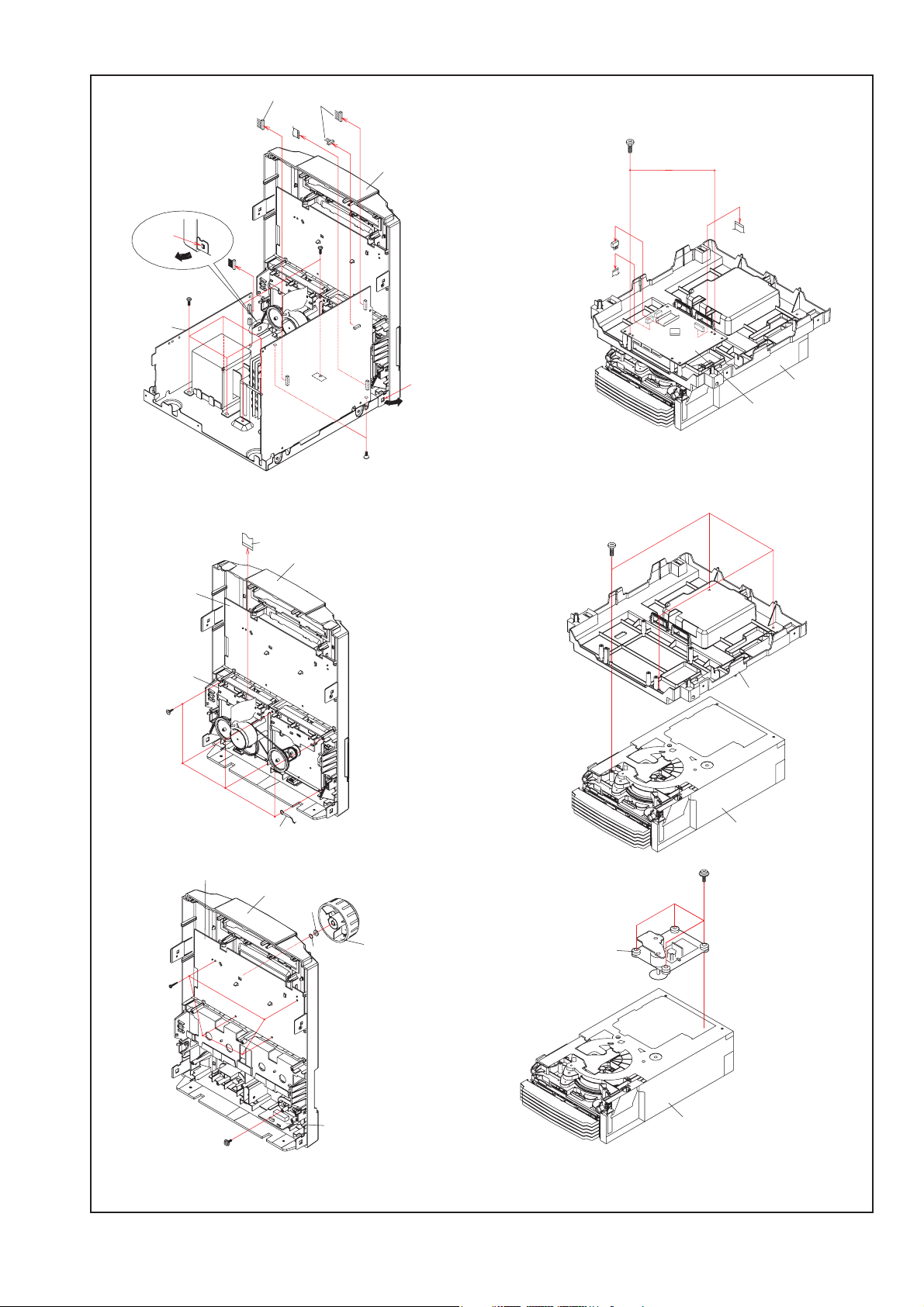
CD-DH790N
Hook
(G4) x 1
PULL
Power PWB
(J1) x 4
M4 x 8mm
Figure 4
(H2) x 1
(G3) x 1
(K2) x 1
(G2) x 1
(H1) x 2
M3 x 6mm
Front Panel
(G3) x 2
Front Panel
(G1) x 2
M3 x 8mm
(G4) x 1
PULL
Hook
(N3) x 1
(N2) x 1
(P1) x 4
M3 x 10mm
Figure 7
(N1) x 2
M3 x 10mm
(N2) x 1
CD PWB
Changer
Mechanism
Unit
Display PWB
Mechanism
(K1) x 6
M3 x 10mm
(M4) x 4
M2.6 x 10mm
Tap e
Figure 5
Display PWB
Lug wire
Front Panel
(M2) x 1
(M3) x 1
(M1) x 1
Figure 8
CD Mechanism
(Q1) x 4
Special
(P2) x 1
Changer
Mechanism
Unit
(L1) x 1
Special Screw
Figure 6
Audio In PWB
3 – 2
Figure 9
Changer
Mechanism
Unit
CD-DH790N
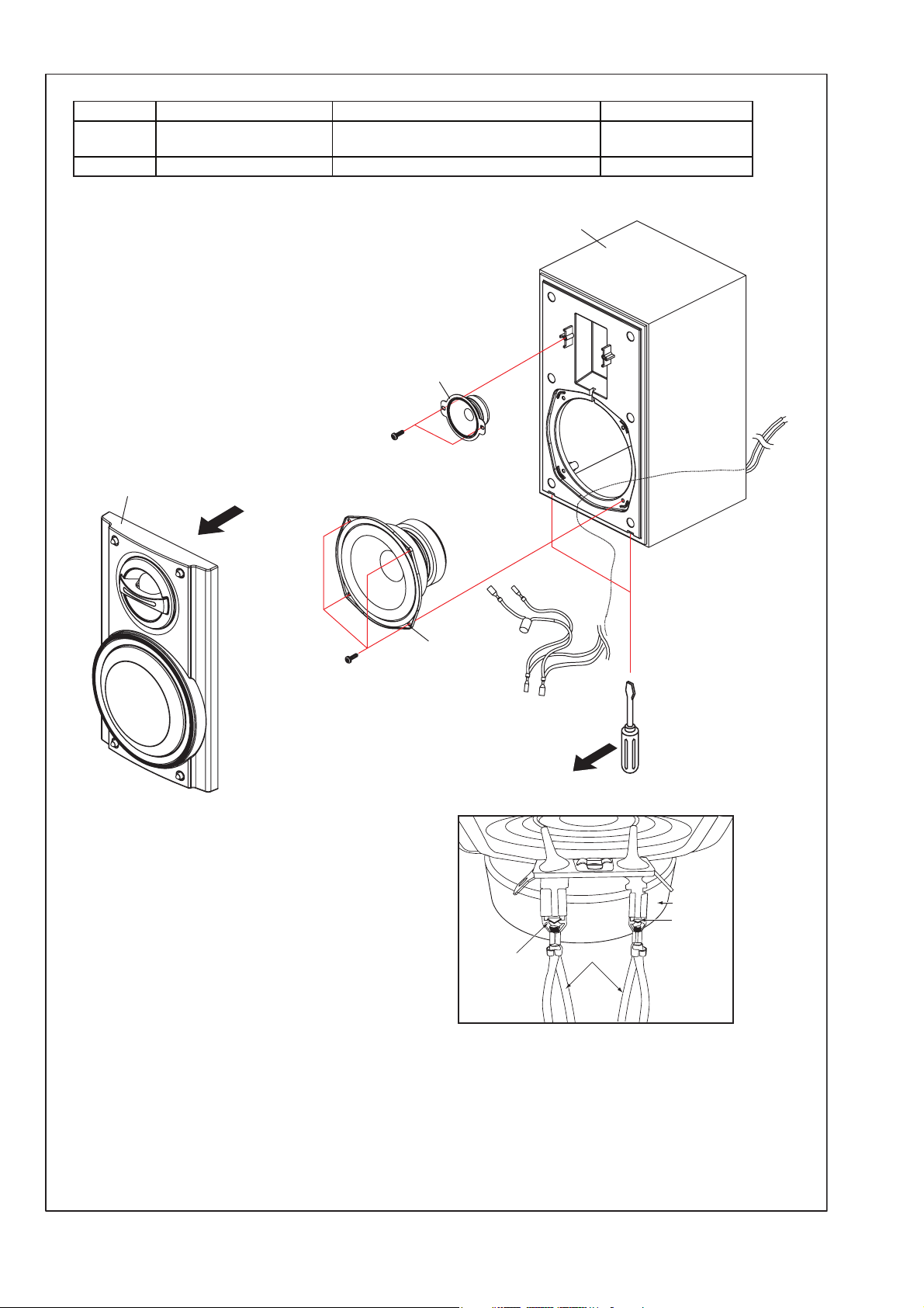
STEP PROCEDURE FIGURE
1 1. Front Panel Ass’y………(A1) X 1
Woofer
REMOVAL
10
1. Screw…….…….…….… (A2) X 4
2 Tweeter 1. Screw…….……….....….(B1) X 2 10
Speaker Box
Tweeter
(B1) x 2
M3 x 10mm
Front Panel Ass’y
(A1) x 1
Figure 10
(A2) x 4
M4 x16mm
Woofer
Screwdriver
SPEAKER UNIT
LOCKING TAB
LOCKING TAB
CAUTION:
TO REMOVE SPEAKER UNIT, PRESS THESE LOCKING TABS
TO RELEASE SPEAKER WIRES.
SPEAKER WIRE
3 – 3

-MEMO-
CD-DH790N
3 – 4
CD-DH790N
2
2
A
CHAPTER 4. DIAGRAMS
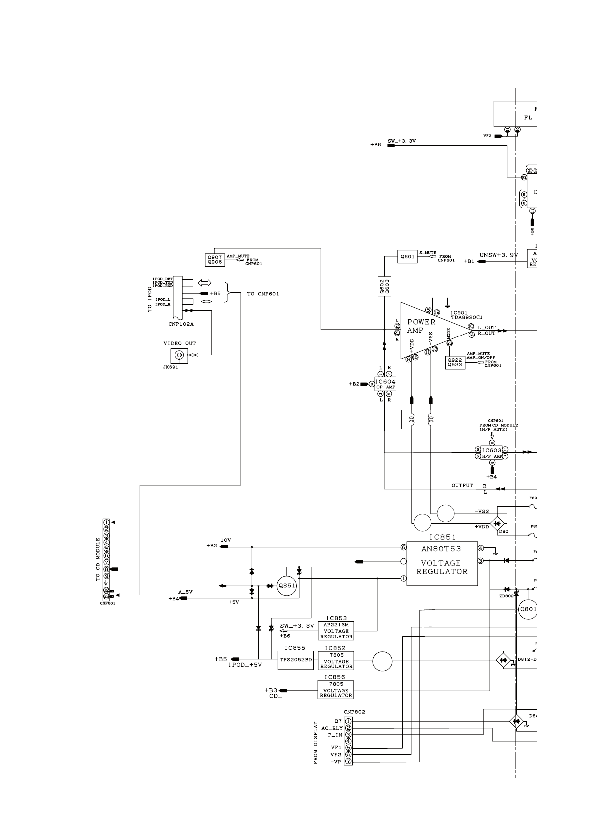
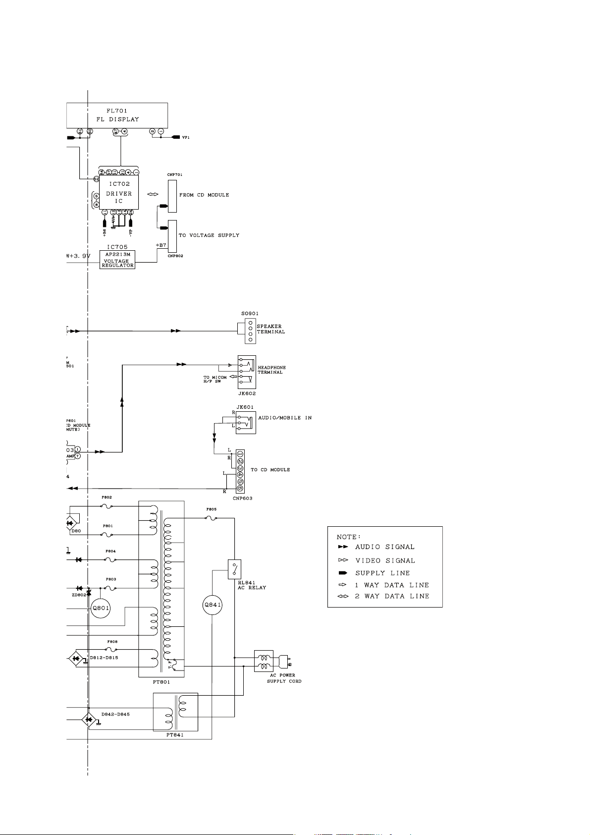
[1] Main Block Diagram
SYS_PROTECT
5.6V
+13V
Q852
L927
R
L
Q905
Q901
2
R
L
5A 1
5A 1
2
2A
2A
1.6
Figure 4-1: MAIN BLOCK DIAGRAM (1/2)
4 – 1
CD-DH790N
R
L
5A 125V
5A 125V
2
2A 125V
2A 125V
1.6A 125V
14
12
17
15
8
9
10
11
5A 125V
7
L844
ZA016AW
3
120V ~ 60Hz
Figure 4-2: MAIN BLOCK DIAGRAM (1/2)
4 – 2
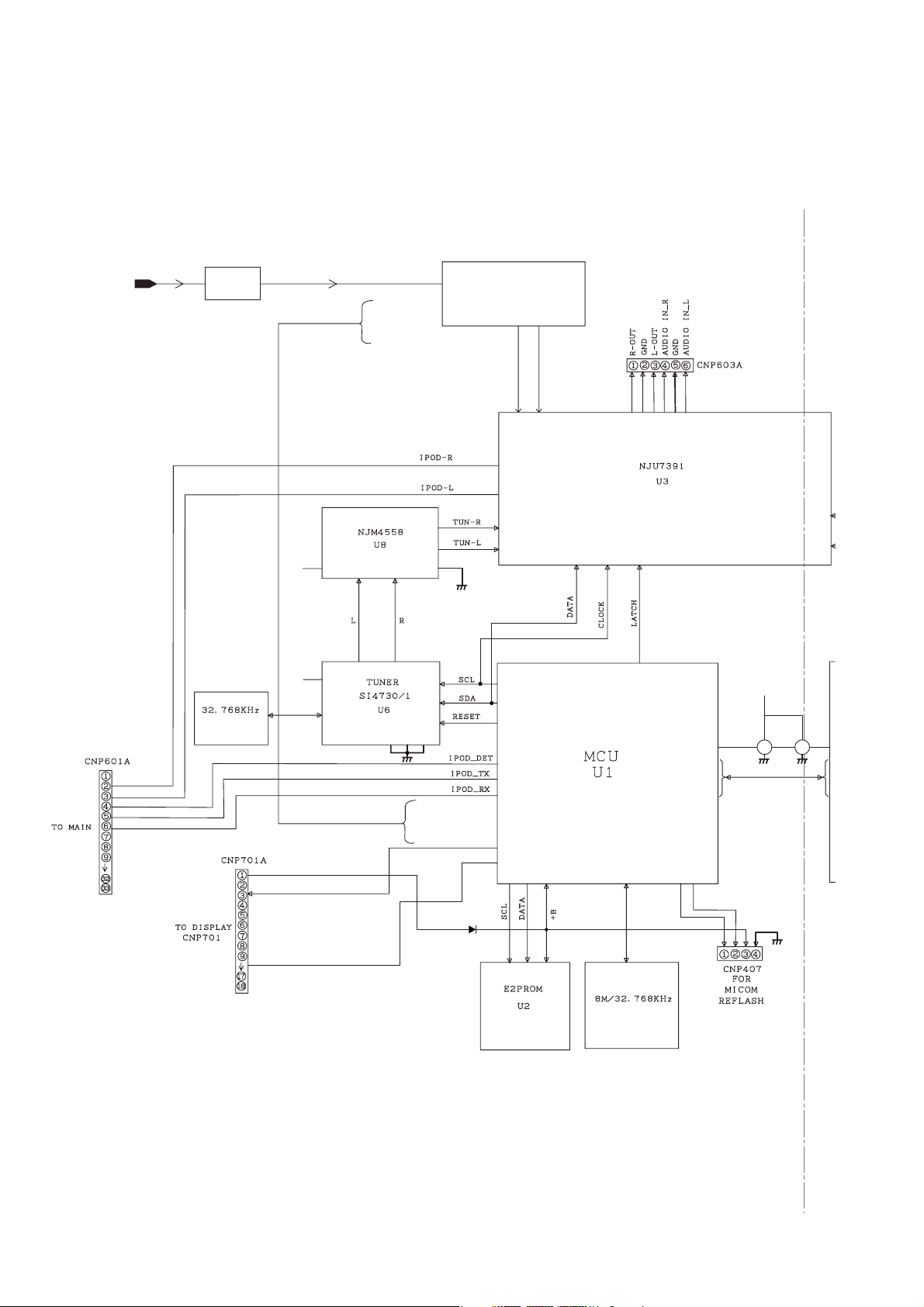
CD-DH790N
[2] Servo Block Diagram
FROM
MAIN PWB
+13V
Q10 ~
Q13
T_SOL
T_MOTOR
T_PHOTO
TAPE MECHA ASSY
TAPE R_IN
TAPE L_IN
+B2
14 13
11
+B6
Y3
9
48
7
8
5
21123
T_SOLin
T_MOTOR 1
PHOTO_OUT
Y1/Y2
37
43 CD_PWR
42 CD_ACK
41 STB
40 CD_DATA
+B3
09 08
MODE36RESET
38
39
45
28
26
27
36 PIN
D1
Figure 4-3: SERVO BLOCK DIAGRAM (1/2)
4 – 3
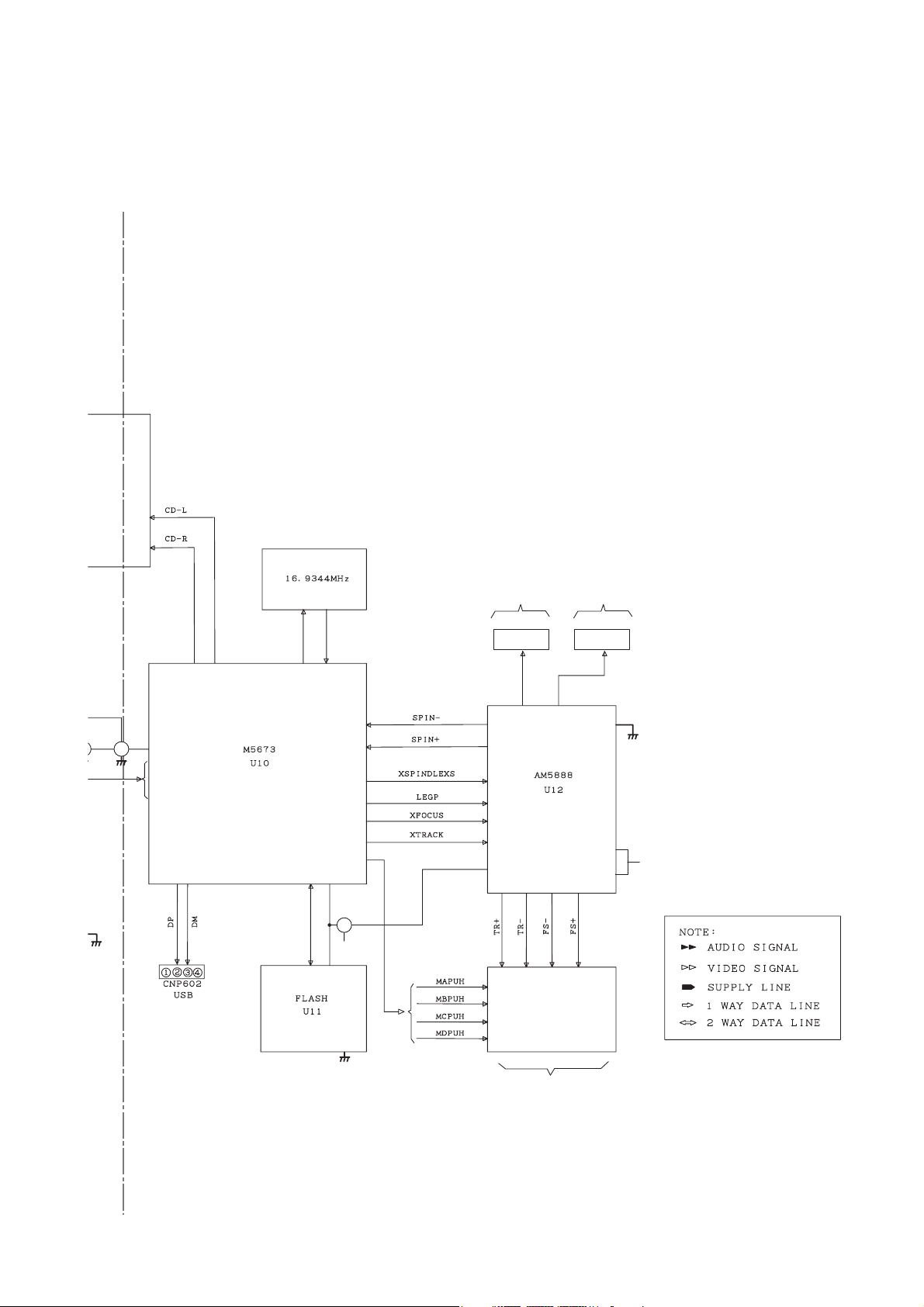
CD-DH790N
To CD PICKUP
CNP404
27 26
08
111 CD +5V
74 CD_ACK
73 CD_DATA
72 STB
53
52
51
50
123
121
126
127
Q6
+B3
8
4
18 22
17
23
4
1
26
2
15
15 14
5
6
7
4
To CD PICK_UP
To CD LOADER
16 13 14
16 13
CNP405
CNP406
19
8
+B3
Figure 4-4: SERVO BLOCK DIAGRAM (2/2)
4 – 4
CD-DH790N
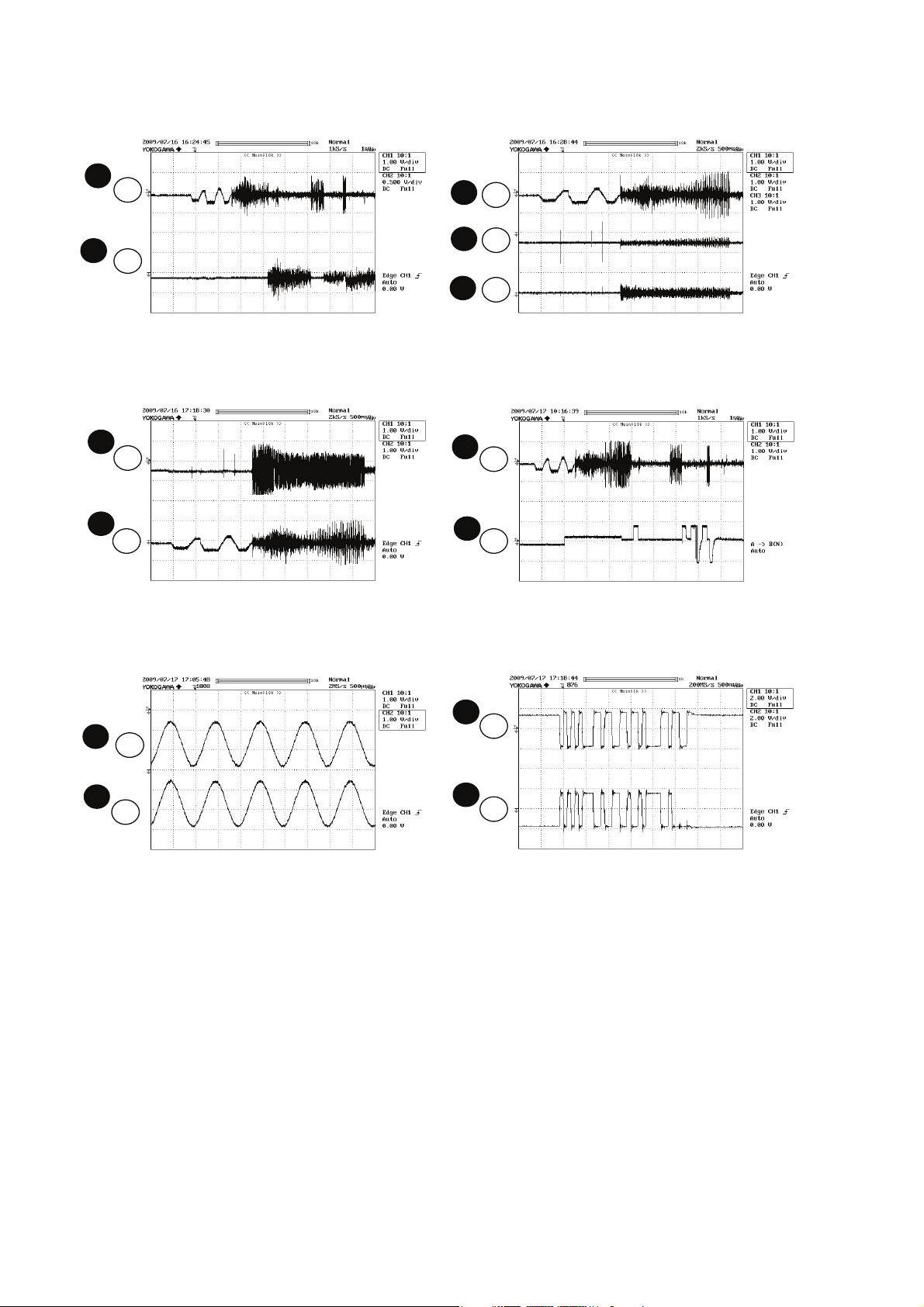
CHAPTER 5.
CIRCUIT DESCRIPTION
[1] Waveform Of Servo Circuit
1
U10 U10
2
U10
4
U10 U10
1
126
126
127
FOO
TRO
Figure 1 Figure 2
TE
14
FOO
1
3
U10
4
FOO
126
FE
13
TE
14
U10
1
5
FOO
126
DMO
123
U10 U10
Figure 3 Figure 4
LINEOUTL
6
33
U10
7
36
U10 U10
LINEOUTR
Figure 5 Figure 6
9
DM
52
U10
10
53
DP
RFO
5 – 1
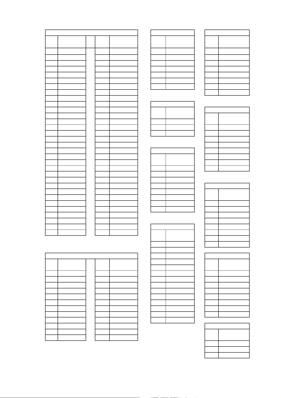
[2] Voltage
IC701 IC851 IC702
PINNOVOLTAGE
(V)
1 -26.66 33 -26.68 1 5.12 1 12.13
2 -26.66 34 -29.10 2 13.03 2 12.23
3 -26.66 35 -26.68 3 18.53 3 3.79
4 -26.66 36 -21.10 4 0.00 4 2.49
5 3.15 37 -17.68 5 19.65 5 0.50
6 3.15 38 -22.10 6 10.05 6 0.50
7 3.06 39 -29.10 7 8.51 7 0.50
8 3.15 40 -24.25 8 0.50
9 3.15 41 -19.40
10 3.15 42 -26.66
11 3.15 43 -24.25
12 1.45 44 -24.57
13 1.45 45 -24.27 1 11.05
14 0.00 46 -19.43 2 0.69 1 5.10
15 -17.50 47 -26.68 3 5.70 2 5.06
16 -29.09 48 -26.68 3 4.94
17 -29.10 49 -29.10 4 0.00
18 -29.10 50 -22.10
19 -29.10 51 -22.10 6 5.06
20 -29.10 52 3.15 7 5.09
21 -29.10 53 -29.10 1 5.12 8 10.04
22 -26.90 54 -29.10 2 5.12
23 -15.26 55 -29.10 3 3.29
24 -29.25 56 -29.10 4 1.92
25 -29.10 57 -26.68 5 0.00
26 -29.10 58 -26.68 6 0.00
27 -19.75 59 -26.68 7 0.00 1 2.02
28 -29.10 60 -26.68 8 0.00 2 2.02
29 -19.70 61 -26.68 3 2.02
30 -21.84 62 -26.68 4 0.00
31 -19.55 63 -26.68
32 -15.23 64 -26.68 6 2.02
PINNOVOLTAGE
(V)
1 2.53 13 -24.48 6 2.52 1 0.50
2 0.00 14 0.00 7 0.00 2 5.70
3 2.44 15 11.45 8 5.12 3 3.16
4 24.15 16 24.35 9 0.00 4 0.00
5 0.00 17 -24.29 10 2.54 5 3.17
6 -24.08 18 -24.15 11 2.57 6 5.09
7 -15.95 19 0.00 12 5.12 7 5.70
8 24.17 20 24.09 13 0.00 8 3.17
9 11.46 21 0.00 14 5.12
10 0.00 22 0.00
11 -24.38 23 2.67
12 -12.10
PINNOVOLTAGE
IC901
PINNOVOLTAGE
(V)
(V)
PINNOVOLTAGE
(V)
IC852
PINNOVOLTAGE
(V)
IC853
PINNOVOLTAGE
(V)
IC902
PINNOVOLTAGE
(V)
1 0.00 8 5.12
2 5.12
3 2.52
4 2.57
5 2.42
PINNOVOLTAGE
IC604
PINNOVOLTAGE
5 4.94
PINNOVOLTAGE
IC603
PINNOVOLTAGE
5 2.02
7 2.04
IC855
PINNOVOLTAGE
IC856
PINNOVOLTAGE
1 14.43
2 1.08
3 6.05
(V)
(V)
(V)
(V)
(V)
(V)
CD-DH790N
5 – 2
CD-DH790N
PINNOVOLTAGE
10 3.16 26 3.16 42 3.17 58 3.17
11 0.00 27 35m 43 3.13 59 0.00
12 0.00 28 3.20 44 37m 60 3.20
13 0.00 29 35m 45 3.15 61 3.20
14 3.21 30 3.15 46 3.17 62 2.16
15 1.50 31 3.16 47 3.17 63 17m
16 2.94 32 32m 48 0.00 64 2.97
PINNOVOLTAGE
PINNOVOLTAGE
10 3.17 2 5.05 2 2.19 22 0.00
11 3.18 3 5.05 3 3.30 23 1.58
12 0.00 4 0.00 4 0.00 24 5.81
13 0.77 5 5.05 5 0.00 25 0.00
14 0.77 6 5.05 6 0.41 26 1.58
15 0.00 7 5.05 7 3.30 27 1.58
16 0.00 8 10.01 8 3.34 28 5.83
17 0.00
18 0.00
19 3.17
20 0.53
U1
PINNOVOLTAGE
(V)
1 2.93 17 34m 33 36m 49 3.14
2 38m 18 34m 34 33m 50 3.20
3 3.15 19 3.15 35 3.15 51 3.20
4 0.75 20 3.16 36 1.17 52 3.15
5 1.14 21 35m 37 3.15 53 19m
6 3.14 22 3.55 38 3.15 54 3.15
7 1.63 23 35m 39 3.15 55 3.15
8 0.00 24 3.54 40 3.17 56 0.00
9 1.56 25 3.15 41 3.15 57 3.15
U2 U3 U12
PINNOVOLTAGE
(V)
1 0.00 1 4.04 17 3.15 1 1.58
2 0.00 2 4.02 18 9.15 2 5.12
3 0.00 3 4.02 19 9.15 3 1.79
4 0.00 4 4.02 20 4.12 4 1.58
5 3.15 5 4.02 21 4.04 5 1.24
6 3.15 6 4.04 22 4.04 6 0.00
7 0.00 7 4.02 23 4.04 7 0.00
8 3.17 8 4.04 24 4.05 8 5.98
9 4.04 25 4.03 9 0.00
U6
(V)
1 0.53 13 0.00 29 4.02 13 3.01
2 0.00 14 0.00 30 4.03 14 2.99
3 0.00 15 3.15 31 4.03 15 2.93
4 0.00 16 3.15 32 4.03 16 2.93
5 3.14 17 2.93
6 3.14
7 3.04 19 5.80
8 3.03 20 0.98
9 1.46 1 5.05 1 0.00 21 1.60
10 0.00 26 4.02 10 0.00
11 4.04 27 4.05 11 3.01
12 4.03 28 4.03 12 3.01
PINNOVOLTAGE
(V)
(V)
U8 U11
(V)
PINNOVOLTAGE
(V)
PINNOVOLTAGE
(V)
PINNOVOLTAGE
(V)
PINNOVOLTAGE
(V)
PINNOVOLTAGE
(V)
18 2.96
5 – 3
U10
PINNOVOLTAGE
(V)
1 3.38 33 1.53 65 1.23 97 NC
2 1.79 34 1.53 66 NC 98 NC
3 1.58 35 1.53 67 NC 99 0.71
4 1.60 36 1.53 68 NC 100 NC
5 1.60 37 0.00 69 NC 101 NC
6 1.60 38 3.34 70 141m 102 NC
7 1.60 39 NC 71 0.00 103 1.25
8 3.39 40 NC 72 NC 104 0.72
9 1.59 41 NC 73 NC 105 0.72
10 1.19 42 NC 74 NC 106 NC
11 0.00 43 NC 75 NC 107 NC
12 1.12 44 NC 76 NC 108 NC
13 1.18 45 0.77 77 NC 109 NC
14 1.38 46 1.53 78 NC 110 0.00
15 0.81 47 0.77 79 NC 111 5.80
16 3.34 48 1.53 80 NC 112 0.00
17 3.34 49 1.72 81 NC 113 3.34
18 1.79 50 2.11 82 NC 114 0.00
19 1.67 51 2.08 83 NC 115 1.77
20 2.31 52 30.4m 84 0.00 116 3.34
21 0.00 53 2.82 85 3.34 117 NC
22 0.00 54 3.34 86 0.72 118 NC
23 3.33 55 0.00 87 NC 119 NC
24 1.78 56 0.00 88 NC 120 1.58
25 3.34 57 3.34 89 NC 121 1.57
26 1.27 58 0.00 90 NC 122 3.34
27 0.72 59 2.19 91 NC 123 1.57
28 0.00 60 0.00 92 1.30 124 0.00
29 1.77 61 0.41 93 1.13 125 NC
30 0.00 62 3.34 94 0.71 126 1.57
31 1.53 63 3.34 95 0.71 127 1.57
32 1.53 64 1.22 96 NC 128 233m
PIN
NO
VOLTAGE
(V)
PIN
NO
VOLTAGE
(V)
PIN
NO
VOLTAGE
(V)
CD-DH790N
IC401
PINNOVOLTAGE
(V)
1 0.00 9 0.00 17 25.80m
2 0.00 10 200.10m 18 0.00
3 0.00 11 0.00 19 0.00
4 0.78 12 0.00 20 2.80
5 2.79 13 6.87 21 0.77
6 0.00 14 4.13 22 0.00
7 0.00 15 0.00 23 0.00
8 25.80m 16 0.00 24 0.00
PINNOVOLTAGE
(V)
PINNOVOLTAGE
(V)
5 – 4

CD-DH790N
-MEMO-
5 – 5
CD-DH790N
CHAPTER 6. CIRCUIT SCHEMATICS AND PARTS LAYOUT
[1] Notes On Schematic Diagram
• Resistor:
To differentiate the units of resistors, such symbol as K and M are
used: the symbol K means 1000 ohm and the symbol M means
1000 kohm and the resistor without any symbol is ohm-type resistor. Besides, the one with “Fusible” is a fuse type.
• Capacitor:
To indicate the unit of capacitor, a symbol P is used: this symbol P
means pico-farad and the unit of the capacitor without such a symbol is microfarad. As to electrolytic capacitor, the expression
"capacitance/withstand voltage is used".
(CH), (TH), (RH), (UJ): Temperature compensation
(ML): Mylar type
(P.P.): Polypropylene type
REF. NO
VR701 VOLUME MAX -- MIN
SW701 ON/STAND-BY ON -- OFF
SW702 FUNCTION ON -- OFF
SW703 DISC/USB/TAPE STOP/TUNING DOWN ON -- OFF
SW704 DISC/USB/iPod PLAY or PAUSE/
TAPE PLAY/TUNING UP
SW705 OPEN/CLOSE ON -- OFF
DESCRIPTION POSITION
ON -- OFF
• Schematic diagram and Wiring Side of P.W.Board for this model are
subject to change for improvement without prior notice.
• The indicated voltage in each section is the one measured by Digital Multimeter between such a section and the chassis with no signal given.
1. In the tuner section,
indicates AM
indicates FM stereo
2. In the main section, a tape is being playback.
3. In the power section, a tape is being playback.
4. In the CD section, the CD is stopped.
Parts marked with “ ” ( ) are important for main-
•
taining the safety of the set. Be sure to replace these parts with
specified ones for maintaining the safety and performance of the
set.
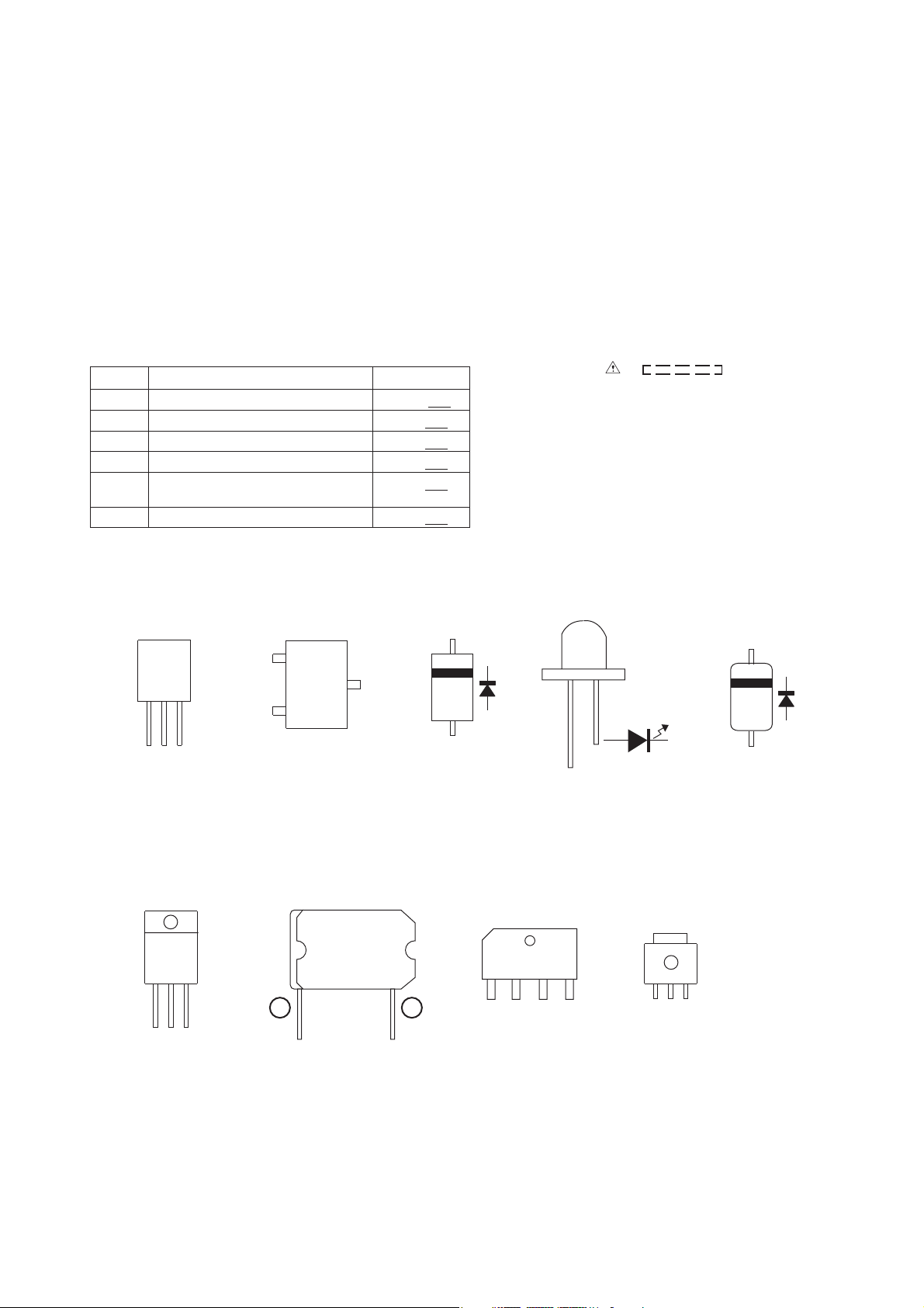
[2] Ty p es Of Transistor And LED
FRONT
VIEW
ECB
(S)(G)(D)
(1)(2)(3)
S8550
KTA1274Y
S8050
KTC3199
KTA1266
KTC3203Y
FRONT
VIEW
BCE
B772
KIA7805A
050N60P
(3)
(1)
B
E
TOP
VIEW
KRA102S
KRC107
KRC104S
H1A
KTA1504GR
KTC3875GR
KRA107S
1
TDA8920CJ
FRONT
VIEW
C
(2)
TOP VIEW
23
1N4004
DRL204F
MA 111
FRONT
VIEW
AC AC -+
10XB60F
TOP VIEW
FRONT
VIEW
HSS4148
343VC3F
TOP VIEW
BCE
HD
6 – 1
CD-DH790N
A
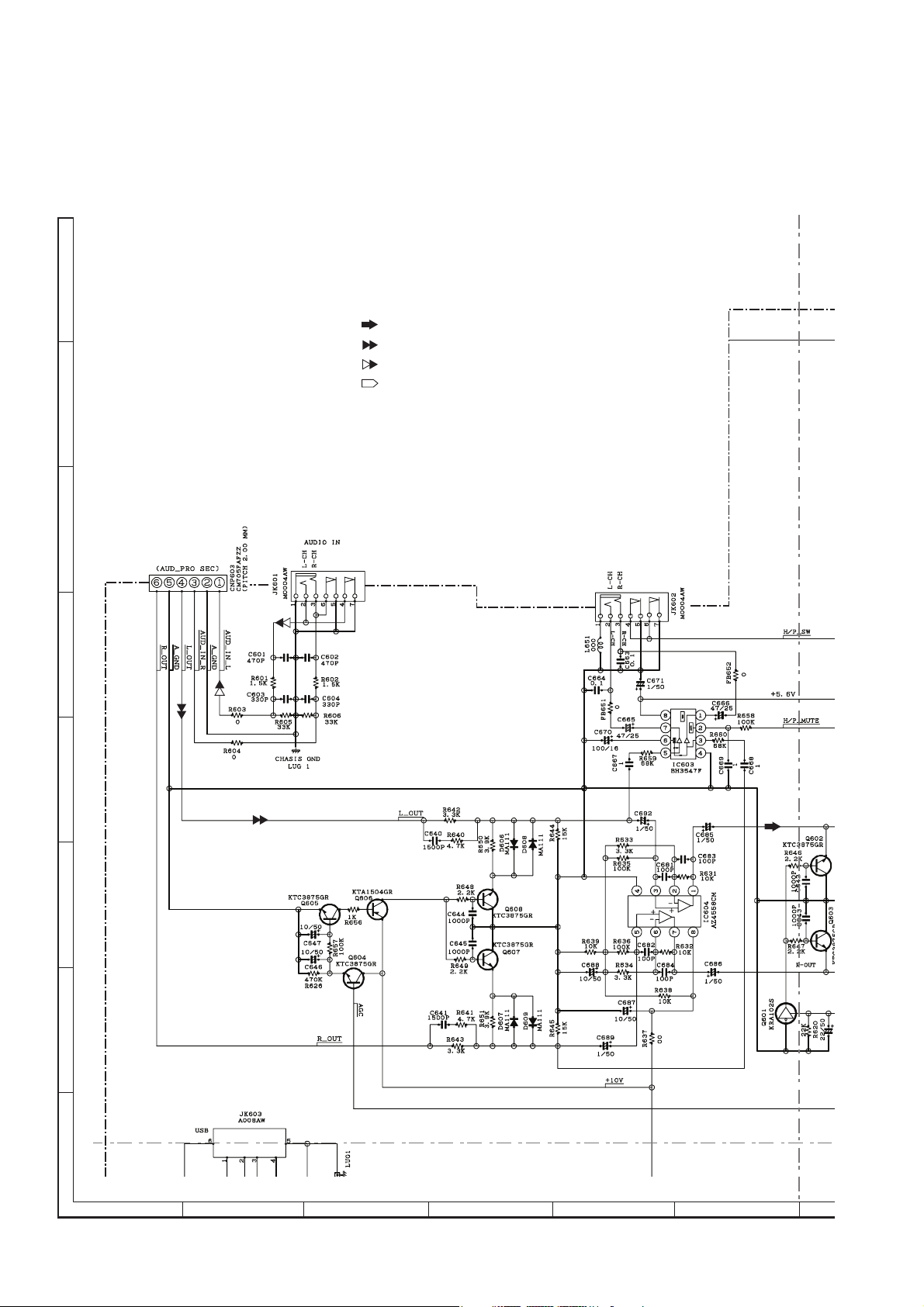
[3] Schematic Diagram
A
FM SIGNAL
CD SIGNAL
AUDIO SIGNAL
iPod SIGNAL
B
C
TO SERVO PWB
D
HEADPHONE
MAIN PWB-
E
F
G
H
1
23456
Figure 6-1: MAIN SCHEMATIC DIAGRAM (1/6)
6 – 2
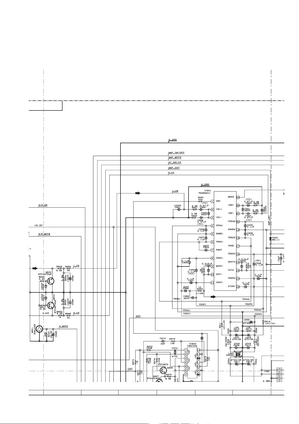
IN PWB-A1
CD-DH790N
C992
100P
7
8 9 10 11 12
47P
47P
47P
Figure 6-2: MAIN SCHEMATIC DIAGRAM (2/6)
6 – 3
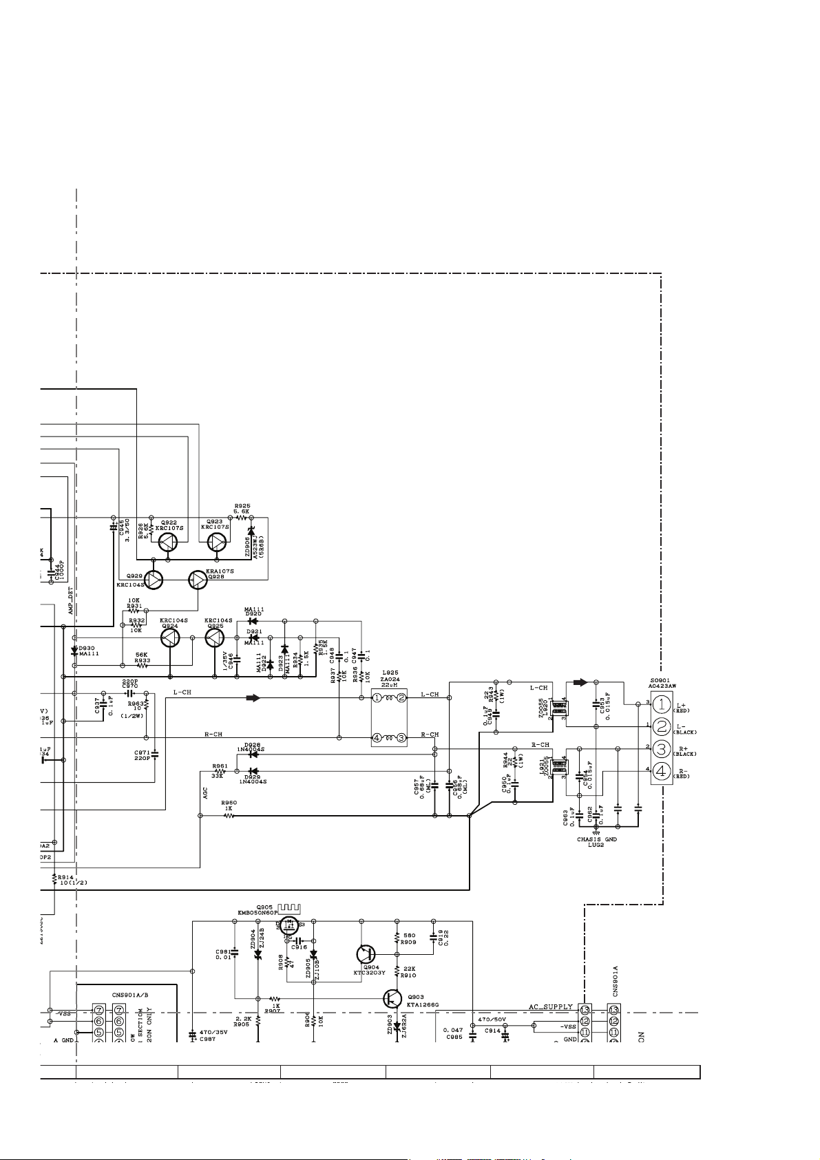
CD-DH790N
13
C988 0.1uF
C989 0.1uF
0.01u
14 15 16 17 18
Figure 6-3: MAIN SCHEMATIC DIAGRAM (3/6)
6 – 4
TO
SPEAKER SYSTEM
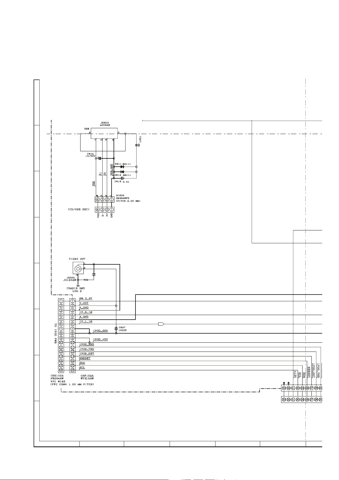
CD-DH790N
A
B
C
TO SERVO PWB
D
C695
0.1u
FB691
E
LN-0061
F
G
SIDE ENTRY
H
1
23456
Figure 6-4: MAIN SCHEMATIC DIAGRAM (4/6)
6 – 5
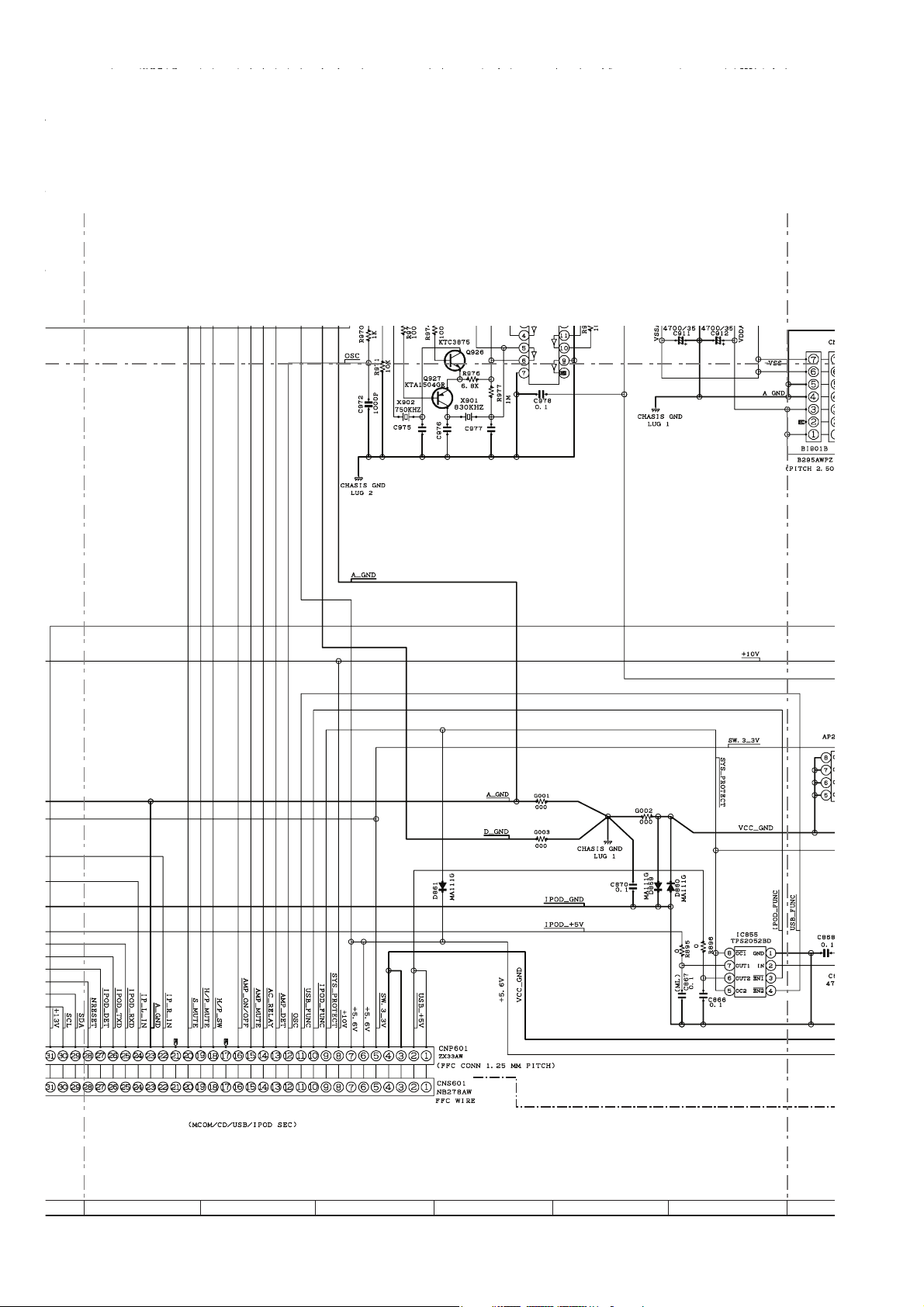
CD-DH790N
C992
100P
47P
47P
47P
TO SERVO PWB
7
8 9 10 11 12
Figure 6-5: MAIN SCHEMATIC DIAGRAM (5/6)
6 – 6
 Loading...