

Page 1

SERVICE MANUAL
CODE: 00ZARP11//A1E
DIGITAL LASER COPIER/
PRINTER OPTION
PRINTER EXPANSION KIT
AR-PK1
MODEL
CONTENTS
[1] SYSTEM CONFIGURATION . . . . . . . . . . . . . . . . . . . . . . . . . . . . . . . . . . . 1-1
[2] SPECIFICATIONS . . . . . . . . . . . . . . . . . . . . . . . . . . . . . . . . . . . . . . . . . . . 1-1
[3] INSTALLATION . . . . . . . . . . . . . . . . . . . . . . . . . . . . . . . . . . . . . . . . . . . . . 3-1
[4] SETTING AND ADJUSTMENTS . . . . . . . . . . . . . . . . . . . . . . . . . . . . . . . . 4-1
[5] SIMULATION . . . . . . . . . . . . . . . . . . . . . . . . . . . . . . . . . . . . . . . . . . . . . . . 4-3
[6] CONFIGURATION REPORT AND TEST PAGE . . . . . . . . . . . . . . . . . . . . 6-1
[7] FLASH ROM VERSION UP PROCEDURE. . . . . . . . . . . . . . . . . . . . . . . . 7-1
AR-P11
[8] PRINTER STATUS MONITOR/PRINTER MANAGEMENT UTILITY. . . . . 8-1
[9] TROUBLE CODE LIST . . . . . . . . . . . . . . . . . . . . . . . . . . . . . . . . . . . . . . . 9-1
[10] CIRCUIT DIAGRAM. . . . . . . . . . . . . . . . . . . . . . . . . . . . . . . . . . . . . . . . . 10-1
PARTS G UI DE
Parts marked with “ ” are important for maintaining the safety of the set. Be sure to replace these parts with
specified ones for maintaining the safety and performance of the set.
This document has been published to be used
SHARP CORPORATION
for after sales service only.
The contents are subject to change without notice.
Page 2

CONTENTS
[1] SYSTEM CONFIGURATION . . . . . . . . . . . . . . . . . . . . . . . . . 1-1
[2] SPECIFICATIONS
1. Basic specification . . . . . . . . . . . . . . . . . . . . . . . . . . . . . . . 1-1
2. Network specification . . . . . . . . . . . . . . . . . . . . . . . . . . . . . 1-1
3. Printer driver specification . . . . . . . . . . . . . . . . . . . . . . . . . 1-1
A. System . . . . . . . . . . . . . . . . . . . . . . . . . . . . . . . . . . . . . 1-1
B. Printing function specification. . . . . . . . . . . . . . . . . . . . 1-2
C. System requrement . . . . . . . . . . . . . . . . . . . . . . . . . . . 1-3
D. Paper handling specifications. . . . . . . . . . . . . . . . . . . . 1-3
E. Print enable area . . . . . . . . . . . . . . . . . . . . . . . . . . . . . 1-4
F. Print reference . . . . . . . . . . . . . . . . . . . . . . . . . . . . . . . 1-4
[3] INSTALLATION
(AR-P11). . . . . . . . . . . . . . . . . . . . . . . . . . . . . . . . . . . . . . . . . 3-1
1. Parts included . . . . . . . . . . . . . . . . . . . . . . . . . . . . . . . . . . 3-1
2. Installation procedure. . . . . . . . . . . . . . . . . . . . . . . . . . . . . 3-1
3. Mounting of additional memory . . . . . . . . . . . . . . . . . . . . . 3-2
(AR-PK1). . . . . . . . . . . . . . . . . . . . . . . . . . . . . . . . . . . . . . . . . 3-2
1. Parts included . . . . . . . . . . . . . . . . . . . . . . . . . . . . . . . . . . 3-2
2. Installation procedure. . . . . . . . . . . . . . . . . . . . . . . . . . . . . 3-2
4. Software installation. . . . . . . . . . . . . . . . . . . . . . . . . . . . . . 3-2
A. Before installing . . . . . . . . . . . . . . . . . . . . . . . . . . . . . . 3-2
B. Driver installation . . . . . . . . . . . . . . . . . . . . . . . . . . . . . 3-2
C. Installing the resident font information for PPD
(Windows 95/98/Me). . . . . . . . . . . . . . . . . . . . . . . . . . . 3-3
D. Uninstalling unnecessary software. . . . . . . . . . . . . . . . 3-3
[4] SETTING AND ADJUSTMENTS
1. Menus and key operation sequences . . . . . . . . . . . . . . . . 4-1
A. Set the print method on the operation panel . . . . . . . . 4-1
B. Configuration menu . . . . . . . . . . . . . . . . . . . . . . . . . . . 4-2
2. AR-PK1 (PS expansion kit) setup . . . . . . . . . . . . . . . . . . . 4-3
A. Setup content . . . . . . . . . . . . . . . . . . . . . . . . . . . . . . . . 4-3
B. Setup enable conditions . . . . . . . . . . . . . . . . . . . . . . . . 4-3
C. Setup menu . . . . . . . . . . . . . . . . . . . . . . . . . . . . . . . . . 4-3
D. Function cancel menu . . . . . . . . . . . . . . . . . . . . . . . . . 4-3
3. Email alert status . . . . . . . . . . . . . . . . . . . . . . . . . . . . . . . 4-3
A. Setup contents. . . . . . . . . . . . . . . . . . . . . . . . . . . . . . . 4-3
B. Setup enable conditions . . . . . . . . . . . . . . . . . . . . . . . 4-3
C. Setup menu . . . . . . . . . . . . . . . . . . . . . . . . . . . . . . . . . 4-3
D. Function cancel display . . . . . . . . . . . . . . . . . . . . . . . . 4-3
[5] SIMULATION
1. Simulation mode key operation. . . . . . . . . . . . . . . . . . . . . 4-3
2. Simulation contents. . . . . . . . . . . . . . . . . . . . . . . . . . . . . . 4-3
[6] CONFIGURATION REPORT AND TEST PAGE
1. Kinds of test pages . . . . . . . . . . . . . . . . . . . . . . . . . . . . . . 6-1
2. Print method . . . . . . . . . . . . . . . . . . . . . . . . . . . . . . . . . . . 6-1
3. Samples . . . . . . . . . . . . . . . . . . . . . . . . . . . . . . . . . . . . . . 6-1
[7] FLASH ROM VERSION UP PROCEDURE
1. Printer control board program download procedure . . . . . 7-1
[8] PRINTER STATUS MONITOR/PRINTER ADMINISTRATION
UTILITY
1. Printer status monitor . . . . . . . . . . . . . . . . . . . . . . . . . . . . 8-1
A. Purpose . . . . . . . . . . . . . . . . . . . . . . . . . . . . . . . . . . . . 8-1
B. Operating environment . . . . . . . . . . . . . . . . . . . . . . . . 8-1
C. V3.0 limitations and notes . . . . . . . . . . . . . . . . . . . . . . 8-1
D. Outline of functions . . . . . . . . . . . . . . . . . . . . . . . . . . . 8-1
2. Printer administration utility. . . . . . . . . . . . . . . . . . . . . . . . 8-3
A. Purpose . . . . . . . . . . . . . . . . . . . . . . . . . . . . . . . . . . . . 8-3
B. Operating environment . . . . . . . . . . . . . . . . . . . . . . . . 8-3
C. Outline of functions . . . . . . . . . . . . . . . . . . . . . . . . . . . 8-3
[9] TROUBLE CODE LIST . . . . . . . . . . . . . . . . . . . . . . . . . . . . . 9-1
[10] CIRCUIT DIAGRAM
1. Block diagram. . . . . . . . . . . . . . . . . . . . . . . . . . . . . . . . . 10-1
2. Circuit diagram . . . . . . . . . . . . . . . . . . . . . . . . . . . . . . . . 10-2
Page 3
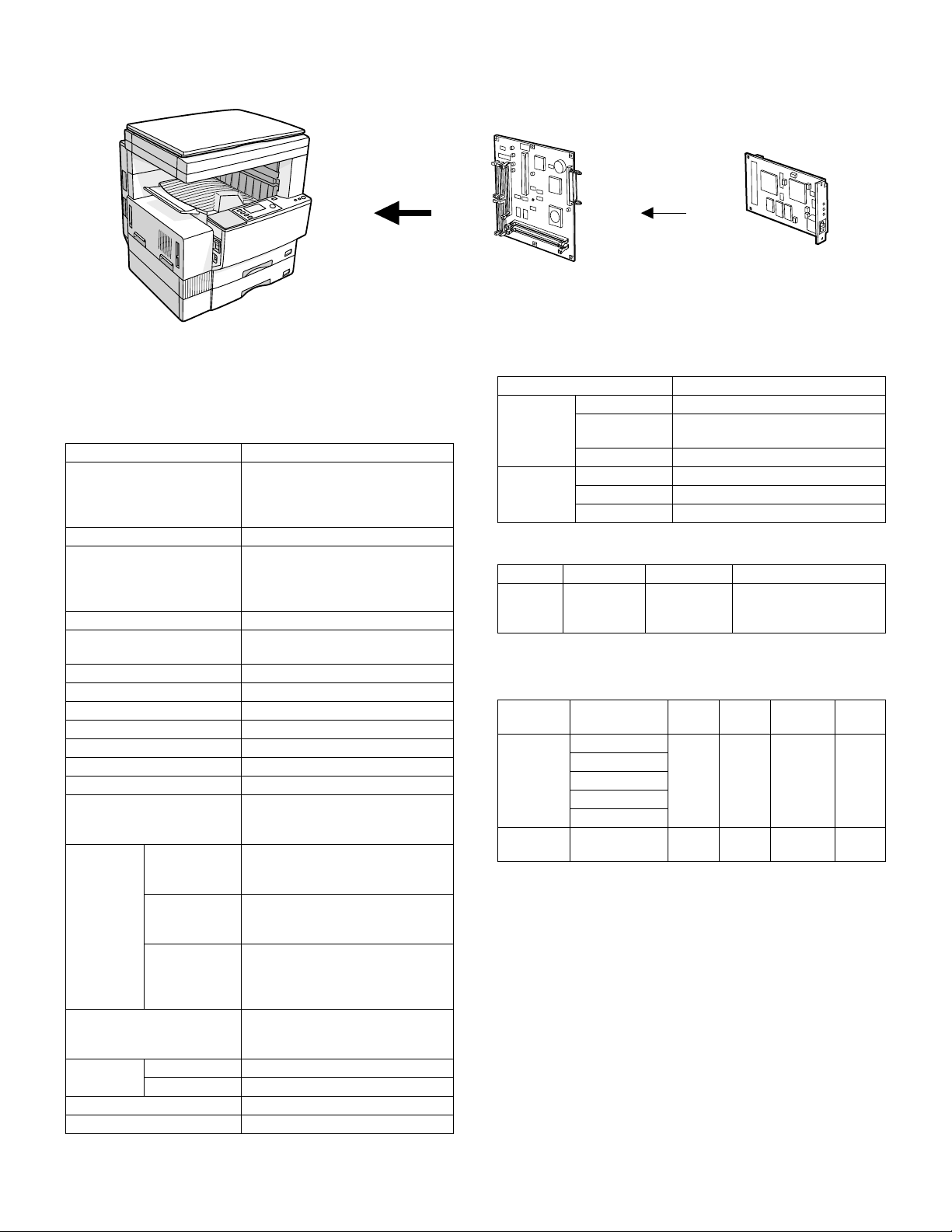
[1] SYSTEM CONFIGURATION
AR-235/275 series
Printer expansion kit
(AR-P11)
Print server card
(AR-NC5J)
[2] SPECIFICATIONS
1. Basic specification
Item Detail
Print Speed AR-275: 27ppm at 600dpi
AR-235: 23ppm at 600dpi
Resolution 300dpi, 600dpi, 1200dpi
Smoothing AR-275: 27ppm at 1200dpi x
Toner Save Mode Standard
Input tray Multi Bypass tray
Duplex Print Standard
Finisher Option
NIC 10/100baseTX
Printer driver Standard
PostScript Level3 Option/Standard
Barcode Font Option
Manual (Online manual) Standard
Platform IBM PC/AT (Include compatible
Support OS
(Printer
Driver)
PDL Emulation
Memory Standard SDRAM 32MB
Expansion Slot for Memory 2 DIMM Slots
Expansion Memory 168pin 32 MB/64 MB/128 MB DIMM
Custom PS Windows 95/98/Me
Custom PCL6
(PCL5e, XL)
PPD only Windows 95/98/Me
Max 288MB
600dpi
AR-235: 23ppm at 1200dpi x
600dpi
Tray 1, Tray 2, Tray 3, Tray 4
machine)
Power Macintosh, iMac, iBook
Windows NT 4.0
Windows2000
Windows 95/98/Me
Windows NT 4.0
Windows2000
Windows NT 4.0
Windows2000
MacOS 8.51 or later
PCL5e emulation
PCL6 emulation
PostScript Level 3 emulation
13.5ppm at 1200dpi
13.5ppm at 1200dpi
Item Detail
Resident
Fonts
Screen
Fonts
For PS 136 Outline Fonts
For PCL5e, XL 45 Outline Fonts
Line Printer
For PCL Barcode Fonts (Option)
For PS 136 Outline Fonts
For PCL 5e, XL 45 Outline Fonts
For PCL Barcode Fonts (Option)
2. Network specification
Interface Support OS Support Protocol
AR-NC5J 10Base-T
100Base-TX
NetWare,
Windows NT,
Mac OS
IPX/SPX, TCP/IP,
EtherTalk, Peer to Peer
(TCP/IP) NetBEUI
3. Printer driver specification
A. System
Machine OS
IBM PC/AT
(Include
compatible
machine)
Mac, Power
Mac
Windows 95
Windows 98
Windows Me
Windows NT 4.0
Windows 2000
MacOS8.51 to
9.x
PCL6
Custom
PCL5e
Custom
Ye s Ye s Ye s Yes
N/A N/A N/A Yes
PostScript
Custom
PPD
File
AR-P11 SYSTEM CONFIGURATION / SPECIFICATIONS - 1
Page 4

B. Printing function specification
Function
General Copies 1-999 ←←←←
Orientation Portrait
Duplex 1-Sided
Binding Edge N/A Long/Short ←←N/A
Pamphlet Style N/A N/A N/A N/A N/A
Pamphlet
Binding Edge
N-up 2/4/6/8/16 2/4/6/8/16 2/4/6/9/16 2/4 *1 2/4/6/8/16
N-up Order Z ←←←←
N-up Border Yes / No ← None / Single
Paper Input Paper Size A3 / B4 / A4 / B5 /
Custom Paper
Size
Source
Selection
Different 1st
(Cover) Page
Transparency
Print
Transparency
Inserts
Paper Output Output Tray
Selection
Staple Finisher
Graphic Resolution
Setting
Halftone
Setting
Graphics Mode Raster
Smoothing Yes / No ←←←←
Toner save Yes / No ←←←←
Photo
Enhancement
Negative Image N/A Yes / No
Mirror Image N/A Horizontal
Zoom N/A ← 25-400% ← N/A
Fit to Page Yes / No ← N/A ← Ye s / N o
Font Resident Font 45 fonts + 1 136 fonts 35 fonts 136 fonts *4 45 fonts + 1
Download Font Bitmap
Others Configuration
Setting
ROPM Yes / No ←←←←
Print Auditor Yes / No ←←N/A Yes / No
PCL5e Custom
Driver
Landscape
2-Sided
A5 / 11 x 17 / B6 / A6
8.5 x 14 / 8.5 x 13 /
8.5 x 11 / 5.5 x 8.5 /
Folio / Exective /
COM-10/ DL / C5/
8K / 16K
1 size ← N/A 3 sizes *2 1 size
Auto
Bypass-Tray (Auto)
Bypass-Tray
(Manual)
Tray 1/2/3/4
Ye s / N o ←←N/A Yes / No
Ye s / N o ←←N/A Yes / No
No
Yes (Blank)
Yes (Printed)
Upper Tray
Center Tray
Offset Tray
Yes / No
600/300 dpi 1200/600 dpi ←←1200/600/300 dpi
N/A Screen Frequency
HP-GL2
N/A Yes / No N/A ← Ye s / No
TrueType
Graphics
Ye s
(Automatic)
PS Custom Driver Macintosh PPD file PPD file
←←←←
←←←←
Left / Right N/A Left / Right
Always Yes Yes / No
hairline / Single thin
line / Double hairline
←←←←
←←←←
←←N/A No
←←←←
←←←←
8 to 360.0
in 0.1 steps
Screen angle
0.0 to 360.0
in 0.1 steps
N/A ←←Raster
Vertical
Bitmap
Type1
TrueType
←←Yes Ye s
/ Double thin line
N/A ←←
←
← Yes / No N/A
N/A Bitmap
← N/A
Type1
TrueType
PCL6 (XL) Custom
Driver
Yes (Blank)
Yes (Printed)
Vector
Bitmap
TrueType
Graphics
(Automatic)
AR-P11 SYSTEM CONFIGURATION / SPECIFICATIONS - 2
Page 5
Function
Others Watermark Yes / No ← Ye s / N o
Page
Protection
Job
Compression
Bitmap
Compression
*1:N-up printing is not supported by Windows NT. For Windows2000, 2/4/6/9/16, Booklet are supported.
*2:Custom paper size is not supported by Windows NT. For Windows2000, only one size is supported.
*3:Halftone setting is not supported by Windows NT.
*4:For Windows95/98/Me, the Font Setup Utility is required. For Win NT, 35 fonts.
PCL5e Custom
Driver
Ye s / N o ← N/A Yes / No ←
N/A None
N/A None
PS Custom Driver Macintosh PPD file PPD file
(with limit)
N/A ←←
Fastest
Fast
Medium
Best Compression
N/A ←←
Very High
High
Medium
Draft
← Ye s / N o
PCL6 (XL) Custom
Driver
C. System requrement
Computer IBM PC/AT compatible machines (DOS/V machines)
Operating
system
Note: Hardware requirements such as CPU and RAM for your operat-
Power Macintosh, iMac, iBook
Microsoft Windows 95
Microsoft Windows 98
Microsoft Windows Me
Microsoft Windows NT 4.0
Microsoft Windows 2000
MacOS 8.51 or later
ing system must be satisfied.
D. Paper handling specifications
(1) Paper feed direction
a. Paper size and image transfer direction
Name
A6R 105 × 148 Yes N/A N/A N/A N/A N/A Yes Yes N/A N/A N/A
B6R 128 × 182 Yes N/A N/A N/A N/A N/A Yes Yes N/A N/A N/A
Invoice 215.9 × 139.7 (8.5” × 5.5”) Yes Yes N/A N/A N/A N/A Yes Yes Yes N/A N/A
Invoice-R 139.7 × 215.9 (5.5” × 8.5”) Yes N/A N/A N/A N/A N/A Yes Yes Yes N/A N/A
A5 210 × 148 Yes Yes N/A N/A N/A Yes Yes Yes Yes N/A N/A
A5R 148 × 210 Yes N/A N/A N/A N/A N/A Yes Yes Yes N/A N/A
B5 257 × 182 Yes Yes Yes Yes Yes Yes Yes Yes Yes Yes Yes
B5R 182 × 257 Yes Yes Yes Yes Yes Yes Yes Yes Yes Yes N/A
Executive-R 186.7 × 266.7 (7.35” × 10.5”) Yes N/A N/A N/A N/A N/A Yes Yes Yes Yes N/A
Letter 279.4 × 215.9 (11” × 8.5”) Yes Yes Yes Yes Yes Yes Yes Yes Yes Yes Yes
Letter-R 215.9 × 279.4 (8.5” × 11”) Yes Yes Yes Yes Yes Yes Yes Yes Yes Yes Yes
A4 297 × 210 Yes Yes Yes Yes Yes Yes Yes Yes Yes Yes Yes
A4-R 210 × 297 Yes Yes Yes Yes Yes Yes Yes Yes Yes Yes Yes
Folio 210 × 330 (8.3” × 13”) Yes N/A N/A N/A N/A N/A Yes Yes Yes Yes N/A
Legal 215.9 × 355.6 (8.5” × 14”) Yes Yes Yes Yes Yes Yes Yes Yes Yes Yes Yes
Foolscap 215.9 × 330.2 (8.5” × 13”) Yes Yes Yes Yes Yes Yes Yes Yes Yes Yes Yes
B4 257 × 364 Yes Yes Yes Yes Yes Yes Yes Yes Yes Yes Yes
A3 297 × 420 Yes Yes Yes Yes Yes Yes Yes Yes Yes Yes Yes
Ledger 279.4 × 431.8 (11” × 17”) Yes Yes Yes Yes Yes Yes Yes Yes Yes Yes Yes
8K 270 × 390 Yes Yes Yes Yes Yes Yes Yes Yes Yes Yes N/A
16K 270 × 195 Yes Yes Yes Yes Yes Yes Yes Yes Yes Yes N/A
16KR 195 × 270 Yes Yes Yes Yes Yes Yes Yes Yes Yes Yes N/A
COM10 4.12 × 9.5 Yes N/A N/A N/A N/A N/A Yes Yes N/A N/A N/A
C5 162 × 229 Yes N/A N/A N/A N/A N/A Yes Yes N/A N/A N/A
DL 110 × 220 Yes N/A N/A N/A N/A N/A Yes Yes N/A N/A N/A
Size
mm (inch)
Bypass
Tray
Tray 1 Tray 2 Tray 3 Tray 4 Duplex
Exit Tray 2tray Finisher
Center
Tray
Upper
Tray
Top
Tray
Offset
Tray
Staple
AR-P11 SYSTEM CONFIGURATION / SPECIFICATIONS - 3
Page 6
Exit Tray 2tray Finisher
Center
Tray
Upper
Tray
Top
Tray
Offset
Tray
Staple
Name
Size
mm (inch)
Bypass
Tray
Tray 1 Tray 2 Tray 3 Tray 4 Duplex
Transparency Yes N/A N/A N/A N/A N/A Yes Yes N/A N/A N/A
Heavy stock Yes N/A N/A N/A N/A N/A Yes Yes N/A N/A N/A
Label Yes N/A N/A N/A N/A N/A Yes Yes N/A N/A N/A
Setting direction toward paper
feed port = Long side
Setting direction toward paper
feed port = Short side
Transfer direction
Transfer direction
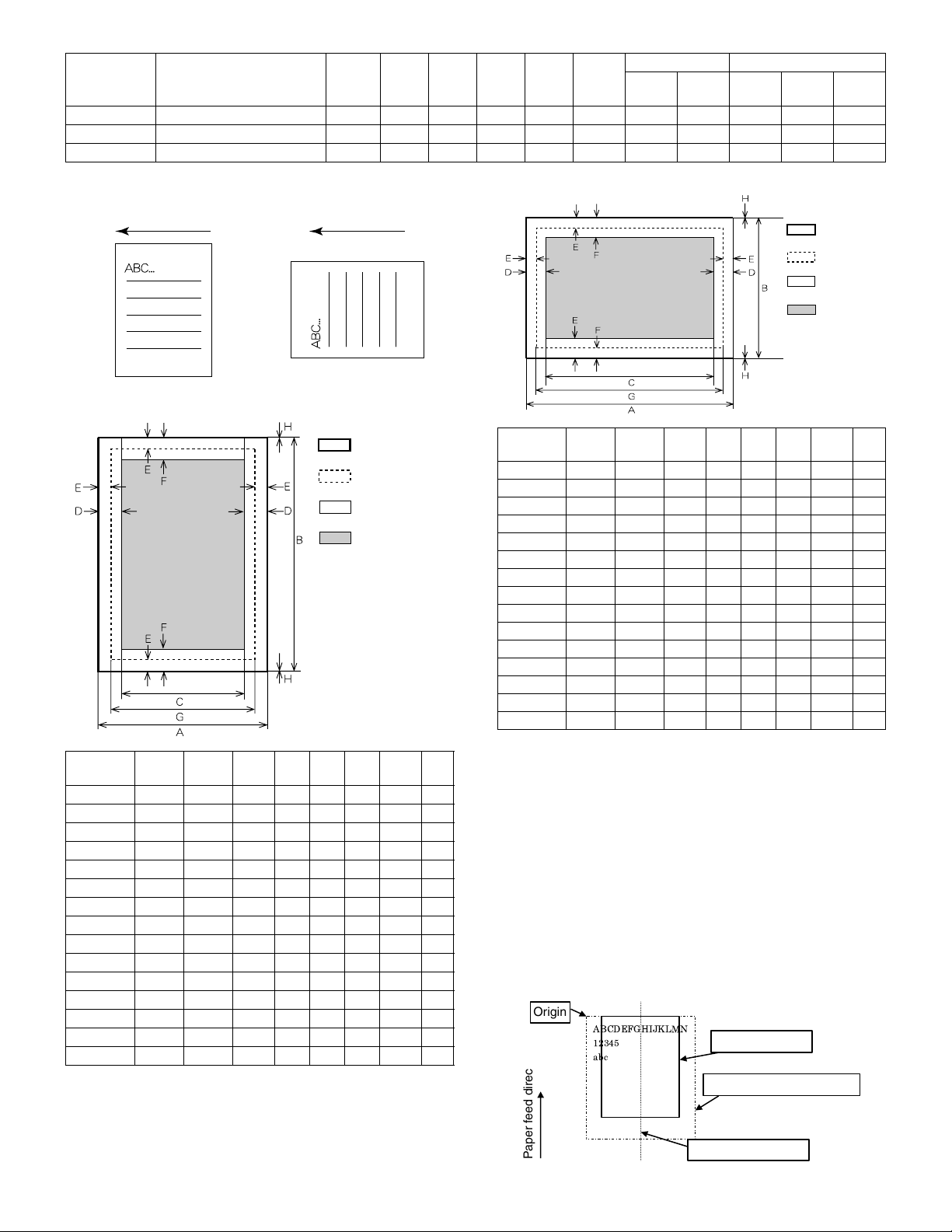
E. Print enable area
Actual page size
Print area
Logic paper size
HP/GL
picture frame
Paper
Size
A3 7014 9920 6730 142 100 300 6814 0
B4 6070 8597 5786 142 100 300 5870 0
A4 4960 7014 4676 142 100 300 4760 0
B5 4298 6070 5770 142 100 300 4098 0
A5 3508 4960 3224 142 100 300 3308 0
Ledger 6600 10200 6300 150 100 300 6400 0
Legal 5100 8400 4800 150 100 300 4900 0
Letter 5100 6600 4800 150 100 300 4900 0
Invoice 3300 5100 3000 150 100 300 3100 0
Foolscap 5100 7800 4800 150 100 300 4900 0
Folio 4980 7800 4680 150 100 300 4780 0
Executive 4350 6300 4050 150 100 300 4150 0
COM-10 2474 5700 2174 150 100 300 2274 0
C5 3826 5408 3542 142 100 300 3626 0
DL 2598 5196 2314 142 100 300 2398 0
ABCDEFGH
Actual page
size
Print area
Logic paper
size
HP/GL
picture
frame
Paper
Size
ABCDEFGH
A3 9920 7014 9684 118 100 300 9720 0
B4 8597 6070 8361 118 100 300 8397 0
A4 7014 4960 6778 118 100 300 6814 0
B5 6070 4298 5830 118 100 300 5870 0
A5 4960 3508 4720 118 100 300 4760 0
Ledger 8400 5100 8160 120 100 300 8200 0
Legal 8400 5100 8160 120 100 300 8200 0
Letter 6600 5100 6360 120 100 300 6400 0
Invoice 5100 3300 2860 120 100 300 4900 0
Foolscap 7800 5100 7560 120 100 300 7600 0
Folio 7800 4980 7560 120 100 300 7600 0
Executive 6300 4350 6060 120 100 300 6100 0
COM-10 5700 2474 3460 120 100 300 5500 0
C5 5408 3826 5172 118 100 300 5208 0
DL 5196 2598 4960 118 100 300 4996 0
Top margin
∗
The set value is received from the digital copier, and data are made
according to the set value.
Left margin
∗
Since the paper size sensor is not set, the digital copier cannot recognize the size and direction of paper which is actually inserted.
Therefore, the left margin is set according to the paper size specified in
the print data sent from the computer, and print process is performed. If
the computer does not specify the paper size, or in the case of the custom size, the left margin is set according to the default paper size.
F. Pri n t re f ere n ce
This machine employs the center reference system.
Since the digital copier is not provided with the tray size detection feature, formatting and center distribution are performed not by the actual
paper size but by the paper size specified by the computer.
Origin
ABCDEFGHIJKLMN
12345
abc
Actual paper size
Paper feed direction
AR-P11 SYSTEM CONFIGURATION / SPECIFICATIONS - 4
Size specified by the HOST
Center reference line
Page 7
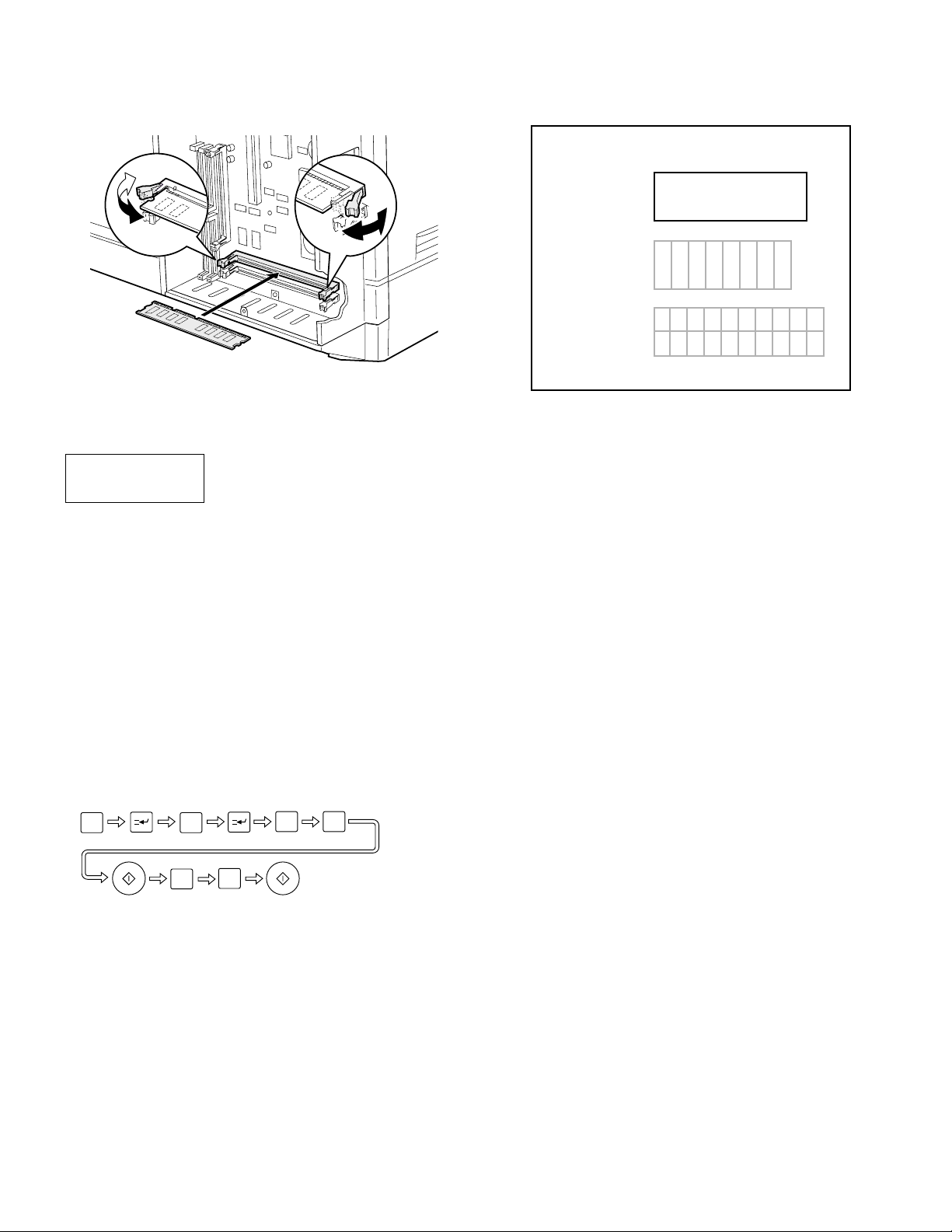
[3] INSTALLATION
(AR-P11)
1. Parts included
PCL PWB: 1 Screws M3 × 8: 2
CD-ROM: 1 Operation manual: 1
2. Installation procedure
Turn off the main switch of the copier and then remove the power
plug of the copier from the outlet.
1) Remove the shielding plate.
Remove five screws and remove the shielding plate.
M3 screws with
washer: 8
Installation
manual: 1
3) Attach the PCL PWB unit.
Connect the parallel connector to the mounting plate for options in
the main unit, connect the connector of the PCL PWB to the connector of the mother board, and attach the PCL PWB using the
supplied eight M3 screws with washer.
Then, attach the parallel connector portion using the supplied two
screws (M3 x 8).
Connector on the mother board
M3 screws with washer
Parallel connector
M3 screws
with washer
4) Attach the shielding plate.
Attach the shielding plate using five screws.
PCL PWB
Screws
(M3 x 8)
Screws
2) Cut and remove the cut-out portion from the left rear cabinet.
Cut and remove the cut-out portion from the left rear cabinet using
a tool such as nippers. (Be careful about the direction of the tool so
that the cut surface is flat.)
Cut-out portion
Screws
Insert the power plug of the copier to the outlet and turn on the
main switch. Then, carry out the following procedure.
5) Check for the PCL PWB.
Press the PRINT key on the operation panel to check to see if the
copier enters the print mode.
6) Check for the language.
Check for the language setting (26-22) following the procedure
described in the service manual (section of simulation).
7) Check for printing.
For installation of printer drivers on a computer, see the supplied
operation manual.
Then, connect a parallel cable to the computer and execute print-
ing to check to see if printing can be executed properly.
AR-P11 INSTALLATION - 1
Page 8
3. Mounting of additional memory
(After mounting it, Installation proceed to step 4.)
Open the two bail clips, insert the memory matching the orientation of
its connector with that of the PWB, and then close the bail clips.
(AR-PK1)
Please keep below important information.
This information will use for other products.
AR-PK1
APPLICATION
NUMBER
MACHINE
SERIAL
NUMBER
PRODUCT
KEY
1. Parts included
CD-ROM: 1
License agreement: 1
Installation manual: 1
2. Installation procedure
To enable the PS3, the product key must be acquired.
(For the method of acquiring the product key, contact the SHARP
authorized dealer.)
1) Check that AR-P11 operates normally.
• Turn on the power and wait until warming up is complete.
• Press the PRINT key on the operation panel of the main unit.
• If the LCD in the operation panel of the main unit switches to the
print mode normally, AR-P11 is operating normally.
• If it is not operating normally, follow the AR-P11 Installation Manual to check and modify the system configuration settings and
check the operation.
2) Enable the PS3.
To enable the system configuration, use the keys on the main unit
to set the mode.
• Enter the product key.
#
C
2
14
Enter the product key that has been acquired in the display using
the numeric keys and press the OK key.
The message " PS KIT KEY OK " will appear in the display.
Setting of the product key is complete. To update the system, press
the CA key to exit the setting mode.
3) Check the PS3.
Make the following sequence of selections on the control panel.
• Press Special Functions , highlight Configuration and press OK.
• Use the up and down keys to highlight Test print menu and press
OK.
• Use the up/down keys to highlight Configuration page and press
OK.
A configuration page will be printed.
Check that the option memory capacity is 128 MB or more.
Check that the PS3 has been installed.
6
4. Software installation
A. Before installing
To use this printer with your computer, you must install a printer driver.
A printer driver is software designed to convert print data from any
application into data understandable by the printer so that the printer
can quickly and efficiently print out the data.
Install the printer driver using the supplied SHARP PRINTER UTILITIES CD-ROM. For installation using the installer in the CD-ROM, see
the document "USING THE DIGITAL COPYING MACHINE AS A
PRINTER".
* It is recommended that you use the PCL6 printer driver. If you have a
problem printing from older software using the PCL6 driver, use the
PCL5e driver.
* You can use the PostScript Level 3 printer driver if you have installed
the PS3 expansion kit (AR-PK1) that is optional for some models.
(1) CD-ROM contains
Also the CD-ROM includes the following utilities and fonts.
• Printer Status Monitor: Utility for monitoring the status of a printer in
network environment
• Printer Administration Utility: Utility for monitoring and adjusting the
settings of printers in network environment
• Resident font information for PPD: Residents font information used
with the PPD driver for Windows 95, Windows 98, and Windows Me
• Display font: Fonts to be displayed on the computer screen to check
the print image on the screen
(2) System requirements
The following hardware and software is required in order to install the
printer drivers.
• IBM PC/AT or compatible computer equipped with a bi-directional
parallel interface or a network interface
• Windows 95, Windows 98, Windows Me, Windows NT 4.0 or Windows 2000 is installed. (Hardware requirements such as CPU and
RAM for your operating system must be satisfied.)
B. Driver installation
If you use Windows 95, Windows 98, Windows Me or Windows 2000
and you connect the printer to your computer with parallel interface, a
printer driver can be installed with the Plug and Play feature.
* The Plug and Play feature is effective if both the computer and
peripheral equipment are equipped with IEEE 1284 compliant parallel interface.
AR-P11 INSTALLATION - 2
Page 9

(1) Installation with Plug & Play
1) Ensure that the printer cable is connected between your computer
and the printer and then turn on the printer.
Note:
Before installing the printer driver, be sure to close all other open
applications.
2) Follow the on-screen instructions.
To specify the printer driver path, see the table below.
To enter the printer name, use the following name.
"SHARP" + printer model name + printer driver
Example: SHARP AR-235 PCL6
(2) Installation with Add Printer wizard
If you use the Add Printer wizard to install a printer driver, follow the
standard procedure of your operating system.
An example of installation is described below for Windows 98.
1) On the Start menu, highlight "Settings", then highlight and click on
"Printers".
2) Insert a PRINTER UTILITIES CD-ROM into a CD-ROM drive.
If your computer is configured for auto start, the license agreement
will be displayed. Click the "Cancel" button.
3) From the Printers window, select "Add Printer" to run the Add
Printer Wizard. Then click "Next".
4) If Windows 98 has been configured for network operation, it might
be necessary to select "Local printer" or "Network printer". Select
the appropriate option, and click "Next" to continue.
5) If "Network printer" was selected, specify the appropriate Network
Path or Queue Name and click "Next".
6) The installation window will display a list of printer models and
manufacturers. Click the "Have Disk" button.
7) Follow the on-screen instructions.
To specify the printer driver path, see the table below.
To enter the printer name, use the following name.
"SHARP" + printer model name + printer driver
Example: SHARP AR-235 PCL6
(3) Printer driver path
* The CD-ROM drive is assigned as drive R here.
Printer
driver
PCL5e Windows 95/98/Me R:\Option\English\9x_me_pcl5e
PCL6 Windows 95/98/Me R:\Option\English\9x_me_pcl6
PostScript Windows 95/98/Me R:\Option\English\9x_me_ps
PPD Windows 95/98/Me R:\Option\English\9x_me_psppd
Operating System Path
Windows NT 4.0 R:\Option\English\nt_pcl5e
Windows 2000 R:\Option\English\2k_pcl5e
Windows NT 4.0 R:\Option\English\nt_pcl6
Windows 2000 R:\Option\English\2k_pcl6
Windows NT 4.0 R:\Option\English\nt_ps
Windows 2000 R:\Option\English\2k_ps
Windows NT 4.0 R:\Option\English\nt_psppd
Windows 2000 R:\Option\English\2k_psppd
C. Installing the resident font information for PPD
(Windows 95/98/Me)
If you have installed the PPD printer driver for Windows 95/ Windows
98/ Windows Me, install the resident font information following the procedure below.
Note:
• Before installing the resident font information, be sure to install the
printer driver.
• When installing the resident font information, be sure to close all
other open applications.
• If you have changed the port for the printer from Properties of the
printer driver when the printer is used as a network printer, reinstall
the resident font information.
• If printer resident fonts cannot be specified from application software, the resident font information has not been installed or the
information is not proper. In this case, reinstall the resident font information.
• With the PPD driver for Windows NT 4.0, the printer resident fonts
cannot be specified. Font downloading, therefore, is always performed when printing is executed. To use the printer resident fonts
under Windows NT 4.0, install the PS, PCL5e or PCL6 driver. For
Windows 2000, the resident font information is automatically
installed with the printer driver.
(1) Installation procedure
1) Start Windows.
2) Insert the supplied PRINTER UTILITIES CD-ROM into a CD-ROM
drive.
If your computer is configured for auto start, the license agreement
will be displayed. Click the "Cancel" button.
3) On the "Start" menu, click "Run".
4) Enter the CD-ROM drive and "packages\english\psppd9x\Pfm-
setup. exe". Then click the "OK" button.
Example: If the CD-ROM drive is designated as drive R, type
"R:\packages\english\psppd9x\Pfmsetup. exe" and click "OK".
5) Click the "OK" button.
If the printer driver has not been installed, installation of the resident font information will not be performed.
6) Click the "OK" button.
7) After the resident font information has been installed, restart Win-
dows.
D. Uninstalling unnecessary software
To uninstall a printer driver or a printer utility that has been
installed using the installer, follow the procedure shown below.
1) On the "Start" menu, highlight "Settings", then highlight and click
on "Control Panel".
2) Double-click "Add/ Remove Programs".
3) Select the driver or utility to be deleted and click "Add/ Remove".
4) Click "Yes".
To delete a printer driver that has been installed using the Plug
and Play feature or from the Add Printer wizard, follow the procedure shown below.
1) On the "Start" menu, highlight "Settings", then highlight and click
on "Printers".
2) Right-click the printer driver to be deleted.
3) Click "Delete" and then follow the instructions on your screen.
AR-P11 INSTALLATION - 3
Page 10
[4] SETTING AND ADJUSTMENTS
1. Menus and key operation sequences
SPECIAL FUNCTION key
CONFIGURATION
OK key
MAIN MENU
OK key
COPIES
key
RESOLUTION
key
SMOOTHING
key
TONER SAVE
key
PAGE PROTECTION
key
ROPM
key
2-SIDED PRINTING
key
PAPER SOURCE
key
PAPER SIZE
key
ORIENTATION
key
EMULATION
key
PCL SYMBOL SET
key
*1
INTERFACE MENU
OK key OK key OK key
I/O TIME OUT
key
PORT SWITCHING METHOD
menu item may not be displayed depending on the
This
*1
installed printer memory capacity.
Displayed only
*2
some models) is installed.
Displayed only if the Print Server Card (AR-NC5J)(optional for
*3
some models) is installed.
*4
Displayed
installed.
key
if
the PS3 expansion kit (AR-PK1)(optional for
only if the optional Barcode Font Kit (AR-PF1) is
PS3 MENU
PRINT PS3 ERROR
key
*2
TEST PRINT MENU
CONFIGURATION PAGE
key
NETWORK STATUS PAGE
key
PCL FONT LIST
key
PS3 FONT LIST
key
OPTION FONT LIST
*3
*2
*4
A. Set the print method on the operation panel
You can control printing using either the operation panel on the printer
or the printer driver installed on your computer. This section explains
the menus that may be set from the operation panel of the printer and
their operation procedures.
NOTE:
When printing from an application on your computer, some of the items
which you can set with the printer driver can also be set with keys of
the operation panel (for example, the number of copies printed). In
these cases, the value set in the printer driver overrides the value set
on the operation panel.
(Basic menu setting procedure)
NOTE:
The menus and items displayed may be different depending on the
optional functions installed.
To access the printer configuration menu, follow the steps below.
1) Press the PRINT key to select the print mode.
Make sure the PRINT indicator lights up and the basic screen is
displayed on the display.
2) Press the [down] key to select the OFFLINE mode.
3) Press the SPECIAL FUNCTION key.
4) Ensure that "CONFIGURATION" is selected and press the OK key.
• The printer configuration menu will appear.
• The menu items are: MAIN MENU, INTERFACE MENU, PS3
MENU, and TEST PRINT MENU. The PS3 menu appears only if
the PS3 expansion kit (AR-PK1) (optional for some models) is
installed.
5) Use the [UP] and [DOWN] keys to select the desired menu and
press the OK key.
NOTE:
The menus and items displayed may be different depending on the
optional functions installed.
6) Use the [UP] and [down] keys to select the desired function and
press the OK key.
• For some functions, a check box is displayed to the left of the
function name. If the OK key is pressed, a check mark will
appear and the function will be set. If the OK key is pressed
again, the check mark will disappear and the function will be
canceled. Proceed to step 8.
• For other programs, the setting screen of the function will appear
when the OK key is pressed.
7) Follow instructions for the function.
• Use the [UP] and [down] keys to select the desired item or use
the numeric keys to enter a number. Then press the OK key.
• If a mistake is made during entry, press the CLEAR key to clear
the entry.
8) To continue with other functions, use the [UP] and [down] keys to
select another program. To select a function of another menu,
press the BACK key and select the desired menu.
• To exit the configuration setting, press the CLEAR ALL key.
AR-P11 SETTING AND ADJUSTMENTS / SIMULATION - 1
Page 11
B. Configuration menu
The following items may be set with the menus of the operation panel.
Values in bold letters are factory default settings. Values that you set
are preserved even if the printer is turned off. Note that the functions
with the settings "On" and "Off" are set by pressing the OK key so that
a check mark is displayed in the check box.
(1) Main menu
Item Possible settings Description
COPIES
RESOLUTION 1200DPI /
SMOOTHING
TONER SAVE On /
PAG E
PROTECTION
ROPM On /
2- SIDED
PRINTING
PAP ER
SOURCE
- 999 Sets how many copies to
1
600DPI
300DPI
/ Off Sets whether smoothing is
On
Off
On /
Off
Off
/ BOOK /
OFF
TAB LE T
/ TRAY1 /
AUTO
TRAY 2 / T RAY3 * /
TRAY4 * / BYPASS
TRAY (MANUAL) /
BYPASS TRAY
(AUTO)
print.
/
Sets the printing resolution.
done or not. This function
improves the appearance of
printed documents by
smoothing the angles and
curves of images. This
allows printing at a higher
apparent resolution. For
example, if the printer is set
to 600dpi, resolution
equivalent to 1200dpi can
be achieved. When printing
bit- mapped images, you
may need to select "Off" to
achieve best results.
Sets whether toner save
mode is in effect or not.
This function prints slightly
fainter to save toner. This
item is different from the
copier "toner save mode".
Sets page protection. Page
protection is a function
designed to prevent data
loss errors when complex
data is printed.
Sets whether the ROPM
function is enabled. If the
ROPM function is enabled,
print data will be stored in
the printer memory once for
printing onto multiple
sheets. This function can
reduce transmission
quantity between the printer
and your computer.
Select "Book" to print on
both sides of the paper and
to bind the left margin.
Select "Tablet" to print on
both sides of the paper and
to bind the top margin.
Sets the tray used for paper
feeding. Setting to "AUTO"
automatically selects the
paper tray loaded with the
paper of the size specified
in the "PAPER SIZE" item. *
The available settings
reflect the installed trays.
Item Possible settings Description
PAPER SIZE A3 / B4 / A4 * / B5 /
ORIENTATION
EMULATION
PCL SYMBOL
SET
PCL symbol set
No. Symbol set No. Symbol set
1 Roman- 8 19 Math-8
2 ISO 8859- 1 Latin 1 20 PS Math
3 PC- 8 21 Pi Font
4 PC- 8 Danish/ Norwegian 22 ISO 8859- 2 Latin 2
5 PC- 850 23 ISO 8859- 9 Latin 5
6 ISO 6 ASCII 24 ISO 8859- 10 Latin 6
7 Legal 25 PC- 852
8 ISO 21 German 26 PC- 775
9 ISO 17 Spanish 27 PC- Turkish
10 ISO 69 French 28 MC Text
11 ISO 15 Italian 29 Windows 3.1 Latin 1
12 ISO 60 Norwegian v1 30 Windows 3.1 Latin 2
13 ISO 4 United Kingdom 31 Windows 3.1 Latin 5
14 ISO 11 Swedish: names 32 Windows Baltic (not 3. 1)
15 PC- 1004 (OS/ 2) 33 Windows 3.0 Latin 1
16 DeskTop 34 Symbol
17 PS Text 35 Wingdings
18 Microsoft Publishing
A5 / B6 / A6 /
11 x 17 / 8- 1/2 x 14
/
8-1/2 x11
8-1/2 x 13 / 8. 3 x 13
/ 7-1/ 4 x 10⁻¹/2 /
5-1/2 x 8-1/2 / 8K /
16K / COM10 / DL /
C5
PORTRAIT
LANDSCAPE
AUTO
- 35 Specifies a PCL symbol set.
1
* /
/
/ PCL / PS3 * Specifies the printer
Sets the size of the paper
where data will be printed. If
this size is different from the
paper size present in the
tray, the size set for this item
takes precedence. *
Depending on where the
printer was purchased, the
default value is either "A4"
or "Letter".
Sets the page orientation
for printing. Specify
"PORTRAIT" to print the
paper with its long side
(longer edge) vertical.
Specify "LANDSCAPE" to
print the paper with its long
side (longer edge)
horizontal.
language used. * Displayed
only if the PS3 expansion
kit (AR- PK1)( optional for
some models) is installed. If
"AUTO" is selected, the
emulation to PCL5e, PCL6
or PS3 is automatically set
depending on the received
data.
(The symbol set is used to
assign a part of character
codes to characters of a
country.) See the table on
the next page. The factory
default setting is 1 (Roman-
8).
AR-P11 SETTING AND ADJUSTMENTS / SIMULATION - 2
Page 12
(2) Interface Menu
Item Setting choice Description
I/ O TIME OUT 1 SEC. -
999
PORT
SWITCHING
METHOD
SWITCH AT END
OF JOB
AFTER I/ O
TIMEOUT
/ SWITCH
60 SEC
-
Sets I/ O time out. If no data
is received within the preset
time, print processing will
be canceled.
Determines which switching
method to use for the
interface port.
(3) PS3 Menu
Displayed only if the PS3 expansion kit (AR-PK1) (optional for some
models) is installed.
Item Setting choice Description
PRINT PS3
ERROR
On /
Off
Prints a PostScript error
page when there are
problems with a print job if
this function is set.
(4) Test Print Menu
Item Description
CONFIGURATION PAGE Prints the configuration page.
NETWORK STATUS PAGE Prints the outline of network settings.
PCL FONT LIST Prints the PCL6 font list.
PS3 FONT LIST Prints the PS3 font list. Displayed only
OPTION FONT LIST Prints the barcode font list. This item
This item is displayed only if the Print
Server Card (AR- NC5J) (optional for
some models) is installed.
if the PS3 expansion kit (AR-PK1)
(optional for some models) is
installed.
is displayed only if the optional
barcode font Kit (AR- PF1) is
installed.
2. AR-PK1 (PS expansion kit) setup
A. Setup content
• The soft key is supplied by registering the manufacturing number
and the model name of the machine and the application number
attached to the PS expansion kit via the Web site.
Enter the soft key to the machine, and the PS3 function can be operated.
If, however, the setup enable conditions are not satisfied, inputs are
disabled.
• When the soft key is erroneously inputted:
When the function lock is canceled: the function lock turns to work.
When the function lock is working: the function lock is kept working.
B. Setup enable conditions
• The printer expansion kit (including the standard equipment) should
be installed.
• The Japanese font ROM should be installed to the printer board.
(Japan only)
• The printer function should be provided as standard provision.
C. Setup menu
Enter the soft key to the machine with SIM 26-11.
D. Function cancel menu
• When the diag menu or the key operator program menu is displayed,
the current machine state (the key is canceled or not) is displayed.
• Display content
ON: The function lock is working.
OFF: The function lock is canceled.
• Regardless of the display position
3. Email alert status
A. Setup contents
• The soft key is supplied by registering the manufacturing number
and the model name of the machine and the fixed application number via the Web site.
Enter the soft key to the machine, and the email alert and status
function can be operated.
If, however, the setup enable conditions are not satisfied, inputs are
disabled.
• When the soft key is erroneously inputted:
When the function lock is canceled: the function lock turns to work.
When the function lock is working: the function lock is kept working.
B. Setup enable conditions
• The printer expansion kit (including the standard equipment) should
be installed.
• The network expansion kit (NIC) should be installed.
C. Setup menu
Enter the soft key to the machine with SIM 26-12.
D. Function cancel display
• When the diag menu or the key operator program menu is displayed,
the current machine state (the key is canceled or not) is displayed.
• Display content
ON: The function lock is working.
OFF: The function lock is canceled.
• Regardless of the display position
[5] SIMULATION
1. Simulation mode key operation
Simulation
1
mode selection
2 Main code selection
3 Sub code selection
Selection of the mode and
4
item
5 Start simulation operation
Returns to the sub code
selection
6
Simulation mode clear
2. Simulation contents
Main
code
22 1 Various counters
24 9 Printer/other
67 14 Printer Flash ROM
Procedure Key operation
Sub
code
Normal
mode
Detail Details of operation
display
counter clear
data download
→
INTERRUPT
#
10-key
10-key
10-key
OK
or
INTERRUPT
CA
The current printer (various)
counter value is displayed.
Printer (other) counter clear.
Enters the Flash ROM
version-up mode of the printer
PWB. (For details, refer to the
Flash ROM version up
procedures described later.)
→ →
(Input main code)
(Input sub code)
and
↑ ↓
START
C
→
→
INTERRUPT
START
START
AR-P11 SETTING AND ADJUSTMENTS / SIMULATION - 3
Page 13
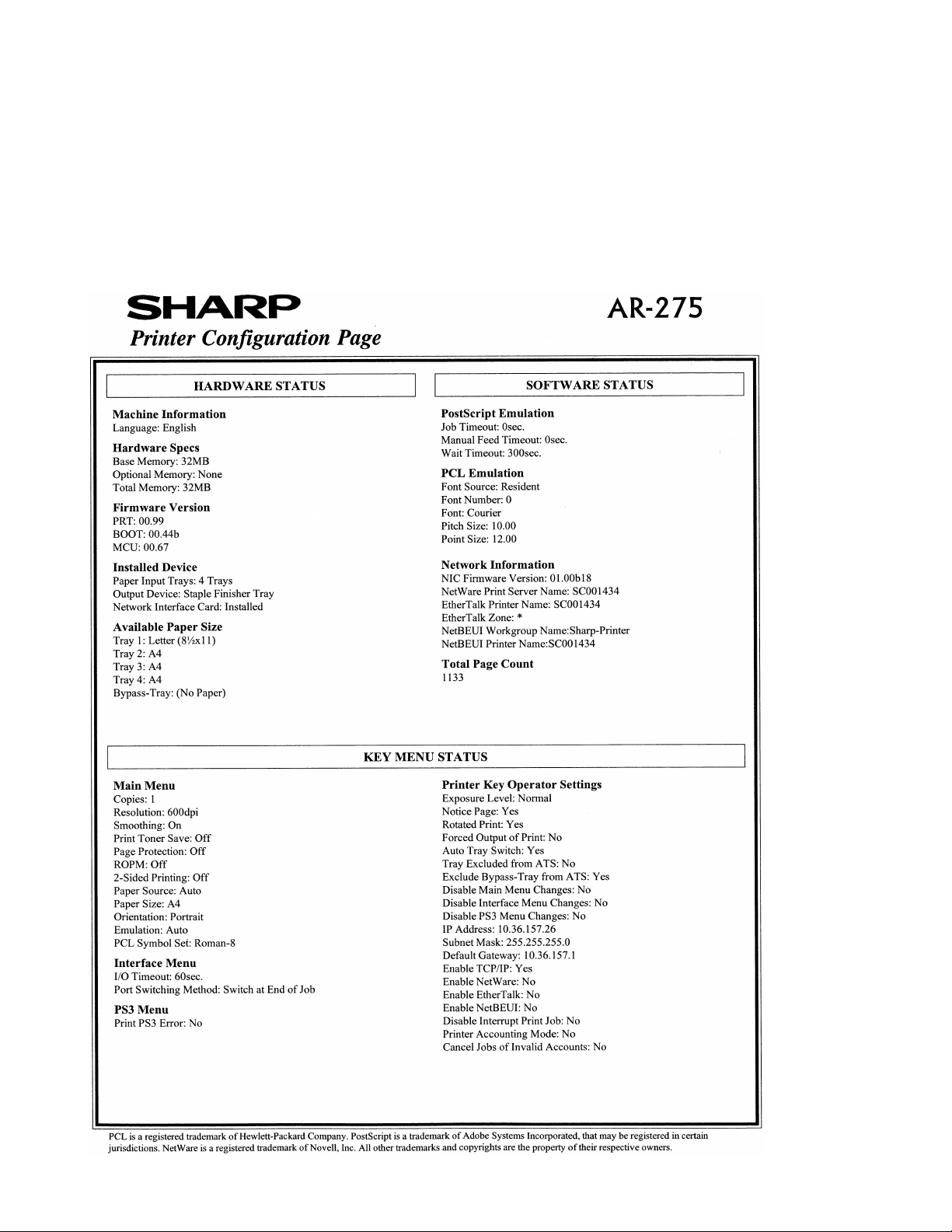
[6] CONFIGURATION REPORT AND TEST PAGE
1. Kinds of test pages
Test pages are available in the following 5 kinds:
• Setup list
• PCL built-in Europe language fonts list
• PostScript built-in Europe language fonts list
• Option fonts list (Only when bar code font option is installed.)
• Network status page (Only when the NIC option is installed.)
3. Samples
2. Print method
1) Push the special function key.
2) Select the test print setup on the operation panel.
3) Select the test page to be printed, and push the OK key.
When the OK key is pushed, the LCD panel display returns to the initial
menu of the printer mode.
AR-P11 CONFIGURATION REPORT AND TEST PAGE - 1
Page 14

[7] FLASH ROM VERSION UP PROCEDURE
(Items necessary for upgrade)
A Personal computer
B Parallel (printer) cable
C Software for upgrade
(Type of ROM)
Flash ROM is directly attached to each PWB
(Targeted PWBs)
1 PCL-PWB
Diagrammatic sketch for upgrade method
(Personal computer)
A
RS232C connector
(9pin or 25pin)
IEEE 1284 port
C
Download
data
I/F Circuit (9pin)
MCU-PWB
IEEE 1284 port
PCL-PWB
B
Parallel cable
1
Operation
panel
Electronic
sort-PWB
FAX-PWB
Finisher
(AR-235/275)
(Necessary files for download)
• Printer control board data transfer tool: fcopy.exe
The maintenance program performs the following program download
operations:
• Printer control board program download
1. Printer control board program download
procedure
The download procedures of the printer control board are as follows:
1) Preliminary procedure: Connect the PC and the main body (printer
control board) with the parallel cable.
Note: If the download cable (RS-232C cable) is connected to the PC
and the main body, be sure to disconnect the cable.
2) Main body side: Turn on the power of the main body.
3) PC side: Confirm that the tree is displayed on the maintenance
program.
4) Enter the test command mode of the main body and execute SIM
67-14 "Flash memory writing."
5) Main body side : Wait until the program transfer start allow message ("Pleas Send Data", etc.) is displayed on the main body
panel.
6) PC side: Double click "Option (printer control board)" in the main
tree items of the maintenance software to develop the sub tree
items. Double click "Printer control board program download" in the
sub tree items.
7) PC side: The maintenance software asks you the printer control
board program download file. Specify the file name.
Printer control board program download file name: pagesXXX.hex
XXX: Release version
9) PC side: Data transmission is started. Wait for a while.
10) PC side: When data transmission is completed normally, the message below is displayed.
Message: Data transmission complete
11) Main body side: Wait until the main body status display is shown
on the main body panel.
12) After-work: Terminate the maintenance program and press the
[CA] key to reset the main body.
With the above procedures, the printer control board program download is completed.
NOTE:
When upgrading the version of the PCL board with NIC installed, it
may take about 30 sec to display "Please Send Data" in the above step
6).
This is because initialization of the NIC is not completed until the
DHCP server has completed retrieval and the IP address has been
acquired (or 30 sec time-out). To avoid this, perform either of the following measures and complete the above step.
Measures to avoid:
• Remove the NIC.
• Turn off DHCP of the NIC.
• Connect to a network with a DHCP server in it.
AR-P11 FLASH ROM VERSION UP PROCEDURE - 1
Page 15

2. Others (Error list)
The list below describes errors occurring during download and countermeasures.
No Error message Descriptions
01 COM Port Open Error ! This error message is displayed when a COM port which is disabled is selected or when there is an abnormal
02 TimeOut Error ! This error message is displayed when no response is sent back from the remote party for 10 sec.
03 Receive Error ! This error message is displayed when data received from the remote party are abnormal.
04 Panel Size Error ! This error message is displayed when the download file size is specified to 8MB though the machine panel is of
05 Destination Error ! This error message is displayed when the destination of the machine panel does not coincide with that of the
06 Printer Control Board
FirmWare Download
Send Error !
COM port.
[Countermeasures]
Select another COM port which is enable. Check if there is any software which is using the COM port.
[Countermeasures]
Once reset the maintenance software and the machine, then download again.
[Countermeasures]
Once reset the maintenance software and the machine, then download again.
4MB size.
[Countermeasures]
Specify a download size suitable for the machine panel size, and download again.
download file.
[Countermeasures]
Specify the download file suitable for the destination of the machine panel, and download again.
This error message is displayed when an error occurs during downloading of the printer control board firmware.
[Countermeasures]
Execute SIM 67-14 on the machine panel to check that "Please Send Data" is displayed, and download again.
AR-P11 FLASH ROM VERSION UP PROCEDURE - 2
Page 16

[8] PRINTER STATUS MONITOR/PRINTER ADMINISTRATION UTILITY
1. Printer status monitor
A. Purpose
• Is printing enabled or disabled?
• Is toner sufficiently supplied?
• Is paper sufficiently supplied?
• Is the previous printing completed?
This application provides easy and simple view of the above items.
B. Operating environment
Windows95, Windows98, WindowsMe, WindowsNT4.0 Workstation
(SP3 or later), Windows2000 Professional, TCP/IP necessary
C. V3.0 limitations and notes
(1) Requisites of printer to be monitored
• The printer driver should have been installed. (Necessary)
• The driver should allow peer-to-peer printing.
For the AR-235/275 series, the attached SC-Print2000 should be
installed to the AR-NC5J, and the "Print destination port" of the
printer should be set to TCP/IP port,
or
• In the case where the driver is shared with the printer server, the
printer should be connected with TCP/IP. In this case, monitoring is
allowed after printing once.
(2) Install and uninstall
In the case of WindowsNT/2000, the administrator authority is required
for install and uninstall.
D. Outline of functions
(1) Status display
Simple view: For beginners
Detailed view: For experts
Simple/Detailed selection allowed
(2) Status change notification
Device status when the machine is sending a job
Print enable
Print disable
Paper jam
Toner empty
Cover open
Off-line
Printer error (Service call)
Notifying method:
Status window pop-up
Tip pop-up
Sound
(3) Selection of printer to be monitored
If the driver is installed, the printer can be monitored.
(4) Job complete notification
Status of the job which was sent by the machine
Print complete
Error
(5) Information supply to the driver
The obtained option information is reflected to the driver setup.
1) Tool bar
Displays the status window, revises the display to the latest state,
makes setups, and displays Help.
2) Status window
Displays the printer status.
Selection of Simple/Detailed view is allowed.
Pop-up to indicate a change in the status is also allowed by setup.
1)
2)
3)
4)
3) Dip
Turns on for a certain time (when setting) when the status
changes.
4) Task tray icon
Memory-resident. Displays the printer status which is monitored.
AR-P11 PRINTER STATUS MONITOR/PRINTER MANAGEMENT UTILITY - 1
Page 17

(6) Job complete notification
When a print job is completed (or interrupted by an error), a notification
from the printer is received and displayed.
The dialog pop-up shows the notification.
1)
1) 2)
3)
4)
5)
6)
1) "Error" icon
1) "Normal" icon
2) Message
3) Notifying time
(7) Status advice immediately before printing (23-page machine/27-page machine)
4) Printer driver name
5) Job name
6) "CLOSE" button
2) Message
3) Notifying time
4) Printer driver name
2)
3)
4)
5)
6)
7)
5) Job name
6) "CLOSE" button
7) "DETAIL" button
The status is checked when printing is performed. The dialog to select Continue or Cancel printing is
(8) Information supply to the printer driver
If any trouble
occurs
displayed.
Option information is obtained from the
printer status monitor and reflected to
the "Device composition setup" tab of
the driver.
AR-P11 PRINTER STATUS MONITOR/PRINTER MANAGEMENT UTILITY - 2
Page 18

2. Printer administration utility
A. Purpose
This application provides easy and simple view of the following items:
• What kinds of network printers are connected in the network?
• Are the network printers operating normally?
• What functions does the printer have?
B. Operating environment
Windows95/98/Me/NT4.0 Workstation (SP3 or later)/2000 Professional, TCP/IP, Winsock2 necessary
C. Outline of functions
(1) Network printer retrieval/list display
• Retrieval and list display of the network printers which conform to the
Printer MIB (RFC1759) specifications.
• Printer status display by the color of the icon
– Normal state (No color)
– Warning state (Yellow)
– Paper low, toner near empty, printer warning
– Error state (Red)
Paper empty, cover open, toner empty, paper jam, printer error
• List display filter function
1)
(2) Alert/log function
• Alert by the pop-up/sound when the printer status changes.
• Making of the alert/log file
(3) Printer property display
• Device information
Model name, status, name, installing place, RAM size, max. print
speed, etc.
• Paper exit tray information
Tray name, number of trays, paper empty/presence of each tray,
paper exit method, printing sequence, etc.
• Paper feed tray information
Number of trays, tray name, paper empty/presence of each tray,
paper size etc,
• Print setup
Channel & PDL information, default PDL, paper direction, single/
duplex print information
• Resource information
Print quantity, toner status, waste toner status
• Summary information
Information on the system and network
• SHARP NIC information
NetWare setup, IP address, hardware address, etc.
3)
2)
1) Main window
List display of network printers.
The status of a printer is indicated by the color of the icon.
2) Printer property page
Detailed information (on the functions and status) of a printer is displayed.
3) Pop-up alert
The pop-up-alert can be displayed by the setup when the printer
status changes.
AR-P11 PRINTER STATUS MONITOR/PRINTER MANAGEMENT UTILITY - 3
Page 19

Printer property page
[Device tab]
1)
2)
3)
4)
3) Description: = Tray name
4) Model name: (Not set in some models.)
5) Paper exit method: Face-up or face-down
6) Printing sequence: "First To Last" or "Last
To F i rs t "
7) Max. paper capacity: The paper presence
is detected and displayed only when the job
separator is installed.
[Paper feed tab]
Information on the
tray selected from
the list is
displayed.
1)
2)
3)
4)
5)
6)
E
O
1) Model
2) Name : Can be set.
3) Installing place: Can be set.
4) Property:
RM size
Max. paper size
Max. print speed
Paper path
[Paper exit tab]
1)
2)
3)
4)
1) Paper feed tray for normal use:
If the driver does not specify any paper feed tray, the printer uses
this tray.
2) List of paper feed trays:
3) Description: = Tray name
4) Model name: (Not set in some models.)
5) Paper size: Length x width (mm)
6) Paper kind: Name defined by ISO/IEC
10175DPA
7) Max. paper capacity: AR-160/200 series
detects the presence of paper only.
[Print setup tab]
Information on the
tray selected from
the list is
displayed.
7)
1)
2)
3)
1) Paper exit tray for normal use:
If the driver does not specify any paper exit tray, the printer uses this
tray.
2) List of paper output trays:
AR-P11 PRINTER STATUS MONITOR/PRINTER MANAGEMENT UTILITY - 4
5)
6)
7)
4)
1) Channel list: List of the effective channels
2) Paper direction: If the driver does not specify the direction, the
printer uses this direction for normal use. (No change allowed for
some models.)
3) Default PDL: If the driver does not specify any PDL, the printer
uses this PDL for normal use. (No change allowed for some models.)
4) Single/Duplex print: If the driver does not specify single/duplex
print, the printer uses this print path for normal use. (No change
allowed for some models.)
Page 20

[Resource type]
! "
1)
1)
2)
2)
3)
3)
1) Print quantity: The quantity of printouts. The paper jams are not
counted. The outputs of copy and FAX are not counted, either.
2) Toner status: OK or toner empty.
(Only toner empty or not is detected in some models.)
3) Waste toner status: (Not supported in the models which have not
a waste toner bottle.)
[Summary tab]
1)
4)
1) NetWare setup: Setup of NetWare enable/disable
If set to enable, setup and display and changes are made on the
following items:
NDS mode or Bindery mode
NDS tree name, context name
Bindery server name,
Ethernet frame name
2) TCP/IP setup: TCP/IP address, sub-net mask, default gateway
3) Hardware address : Hardware address of the network card in the
target printer.
4) Link to the device Web page (Provided only the models which have
an assembly Web server.)
[Application]
1) Network and device information:
Device information
– Descriptions, operating time, etc.
Network information
– TCP, IP, the number of send/receive packet of SNMP
AR-P11 PRINTER STATUS MONITOR/PRINTER MANAGEMENT UTILITY - 5
3)2)1)
1) Setup : Used to set that the icon is minimized when booting or not,
and that the setup content is stored when terminating or not.
2) Network printer retrieval interval: Used to set automatic retrieval of
a printer on the network.
The printers to be retrieved can be set with the "Printer retrieval
(TCP/IP)" tab.
The retrieval interval is 1min to 60min. The default is 3min.
3) State and alert revision interval
Used to set automatic revision of the printer status. The revision
interval is 10sec to 90sec. The default is 30sec.
Page 21

[Confirmation]
1)
[Printer retrieval]
1) Confirmation message: Used to set that the confirmation pop-up
menu is displayed when;
the device setup is changed.
the device is deleted,
the filter setup is deleted,
the log file is deleted,
the application is terminated.
1) 2)
1) Printer retrieval on the local network :
When this box is checked, the local network address is obtained
from the IP address and the sub net mask of the PC where PAU is
installed, and a printer on the local network is retrieved.
2) Retrieval by IP address :
A certain IP address can be obtained.
Only when this box is checked, the printers which have IP
addresses listed on the list can be retrieved.
AR-P11 PRINTER STATUS MONITOR/PRINTER MANAGEMENT UTILITY - 6
3)
3) Advanced retrieval dialog box
Used to set the printer retrieval on an external network.
To specify an external network to be retrieved, enter the network
address and the sub net mask of that network.
Page 22

System diagram
User
User
Printer status monitor
Printer status monitor
Printer
status
monitor
User
Manager
User
Printer status monitor
PAU
Printer status monitor
Printer status monitor
User
User
AR-P11 PRINTER STATUS MONITOR/PRINTER MANAGEMENT UTILITY - 7
Page 23

[9] TROUBLE CODE LIST
Trouble code
Main
Sub
code
code
F9 00 Content F9-**: MCU-PRT communication trouble
Details Communication establishment error/
Cause Printer PWB connector disconnection
Check
and
remedy
10 Content Printer PWB trouble
Details Communication trouble between MCU and
Cause Printer PWB connector disconnection
Check
and
remedy
80 Content Printer PWB communication trouble
Details Communication trouble between MCU and
Cause Printer PWB connector disconnection
Check
and
remedy
81 Content Printer PWB communication trouble
Details Communication trouble between MCU and
Cause Printer PWB connector disconnection
Check
and
remedy
Details of trouble
framing/parity/protocol error
Harness trouble between the printer PWB
and the MCU PWB
Motherboard connector pin breakage
Printer PWB ROM trouble/Data
disturbance
Check the connectors and harness of the
printer PWB and MCU PWB.
Check the grounding of the copier.
Check ROM on printer PWB.
printer PWB
Harness trouble between the printer PWB
and the MCU PWB
Motherboard connector pin breakage
Printer PWB ROM trouble/Data
disturbance
Check the connectors and harness of the
printer PWB and MCU PWB.
Check the grounding of the copier.
Check ROM on printer PWB.
(Protocol)
printer PWB (Protocol error)
Harness trouble between the printer PWB
and the MCU PWB
Motherboard connector pin breakage
Printer PWB ROM trouble/Data
disturbance
Check the connectors and harness of the
printer PWB and MCU PWB.
Check the grounding of the copier.
Check ROM on printer PWB.
(Parity)
printer PWB (Parity error)
Harness trouble between the printer PWB
and the MCU PWB
Motherboard connector pin breakage
Printer PWB ROM trouble/Data
disturbance
Check the connectors and harness of the
printer PWB and MCU PWB.
Check the grounding of the copier.
Check ROM on printer PWB.
Trouble code
Main
Sub
code
code
F9 82 Content Printer PWB communication trouble
Details Communication trouble between MCU and
Cause Printer PWB connector disconnection
Check
and
remedy
84 Content Printer PWB communication trouble
Details Communication trouble between MCU and
Cause Printer PWB connector disconnection
Check
and
remedy
88 Content Printer PWB communication trouble
Details Communication trouble between MCU and
Cause Printer PWB connector disconnection
Check
and
remedy
99 Content Machine-PCL board language error
Details The machine language setup does not
Cause PCL board connection error
Check
and
remedy
Details of trouble
(Overrun)
printer PWB (Overrun error)
Harness trouble between the printer PWB
and the MCU PWB
Motherboard connector pin breakage
Printer PWB ROM trouble/Data
disturbance
Check the connectors and harness of the
printer PWB and MCU PWB.
Check the grounding of the copier.
Check ROM on printer PWB.
(Framing)
printer PWB (Framing error)
Harness trouble between the printer PWB
and the MCU PWB
Motherboard connector pin breakage
Printer PWB ROM trouble/Data
disturbance
Check the connectors and harness of the
printer PWB and MCU PWB.
Check the grounding of the copier.
Check ROM on printer PWB.
(Timeout)
printer PWB (Timeout error)
Harness trouble between the printer PWB
and the MCU PWB
Motherboard connector pin breakage
Printer PWB ROM trouble/Data
disturbance
Check the connectors and harness of the
printer PWB and MCU PWB.
Check the grounding of the copier.
Check ROM on printer PWB.
coincide with the PCL board language
setup.
SIM setup error
Check the firmware of the PCL board and
the combination of the panel screen data,
and download the correct version, if
necessary.
Check the machine language information.
(Machine language setup: SIM 26-22)
AR-P11 TROUBLE CODE LIST - 1
Page 24

[10] CIRCUIT DIAGRAM
1. Block diagram
(66MHz)
System CLK
32MB
SDRAM
On Board
SDRAM
168pin DIMM
(Max 128MB)
SDRAM
168pin DIMM
(Max 128MB)
Boot ROM (4MB)
On Board
CPU
200MHz
TMPR4955AF
Code ROM (8MB)
72pin SODIMM
Font ROM (4MB)
(ESCP)
72pin SODIMM
Kanji Font
ROM (32MB)
100 pin SODIMM
72pin SODIMM
Option ROM (8MB)
AR-P11 CIRCUIT DIAGRAM - 1
Page 25

+5V
RB160L-40
D3
RB160L-40
R225 1K
R223 10
R224 10
+
10uF
C77
C79
0.1u
C78
1000p
C128
100p
R226 10
155
IC29
VssPLL
1 2
TP701
156
PLLCAP
D2
TPC3
TPC2
797877
TPC1
1 2
R222 10
TP699
157
VccPLL
E
D
32
VINVOUT
TP700
ADJUST
1
TP707
+3.3V
R227 4.7k
R228 4.7k
TP702
TP703
118
1196887
DIVMODE1
DIVMODE0
+
10uF
C134
NJM317DL1
R232 200
R229 4.7k
R230 4.7k
TP704
TP705
80235
Endian
BUFSEL1
HALT/DOZE
DebugCLKOUT
R231 4.7k
TP706
BUFSEL0
144
VccINT
136
C130
C129
C133
C132
C131
C84
130
VccINT
VccINT
123
VccINT
112
+
+
105
VccINT
VccINT
22u
22u
0.1u
0.1u
0.1u0.1u
VccINT
VccINT
VccINT
VccINT
VccINT
VccINT
VccINT
111825325065819198
VccINT
VccINT
160
VccIO
154
VccIO
C53
C80
C45
C50
C54
C82
152
VccIO
140
133
VccIO
VccIO
+
+
126
VccIO
116
VccIO
22u
22u
0.1u
0.1u
0.1u
0.1u
109
VccIO
VccIO
VccIO
VccIO
VccIO
VccIO
VccIO
VccIO
VccIO
VccIO
VccIO
VccIO
VccIO
71421284048596775868895102
VccIO
51
Vss
Vss
TimerIntDisable
Vss
19222629334152606676899296
Vss
Vss
Vss
Vss
Vss
Vss
Vss
Vss
Vss
Vss
Vss.
E
D
99
103
106
110
113
120
124
127
131
134
137
141
145
153
158
Vss
Vss
Vss
Vss
Vss
Vss
Vss
Vss
Vss
Vss
Vss
Vss
Vss
Vss
Vss
Vss
Vss
Vss
C
B
A
TMPR4955AF
SYSADC3
SYSADC2
IC21
132
129
TP55
TP58
RN784.7kx4
685
23174
+3.3V
SYSADC1
SYSADC0
138
135
TP56
TP57
SYSCMD8
SYSCMD7
62
61858
TP128
TP129
TP130
RN6410x4
10
865
21374
R93SYSCMD8
SYSCMD7
SYSCMD6
SYSCMD6
SYSCMD5
SYSCMD4
571256
TP131
TP132
TP133
RN6710x4
865
SYSCMD5
SYSCMD4
SYSCMD3
SYSCMD3
SYSCMD2
SYSCMD1
551554
TP134
TP135
21374
SYSCMD2
SYSCMD1
SYSCMD0
53
TP136
+3.3V
SYSCMD0
SYSCMDP
EXTRQST_
RELEASE_
RdRDY
WrRDY
VALIDIN_
TP27
TP138
R134 10
TP623
TP348
TP365
TP59
R138 10
TP698
VALIDOUT_
648347434445468285
TP60
R90 4.7k
ColdReset_
Reset_
84
TP22
TP21
PLLReset
49
MasterCLK
159
TP393
JTDI
TRst_
442563
TP29
TP392
TCK
TMS
TDO
PCST8
PCST7
PCST6
PCST5
147
148
149
150
151
R133 4.7K
R141 4.7K
R140 4.7K
R135 4.7K
R139 4.7K
R136 4.7K
R137 4.7K
R233 4.7K
PCST4
363738
PCST3
PCST2
PCST1
PCST0
39
NMI
TP332
74
TP61
INT5
INT4
INT3
INT2
INT1
INT0
MODE43_
SYSAD31
SYSAD30
SYSAD29
SYSAD28
SYSAD27
SYSAD26
SYSAD25
SYSAD24
SYSAD23
SYSAD22
SYSAD21
SYSAD20
SYSAD19
SYSAD18
SYSAD17
SYSAD16
SYSAD15
SYSAD14
SYSAD13
SYSAD12
SYSAD11
SYSAD10
SYSAD9
SYSAD8
SYSAD7
SYSAD6
SYSAD5
SYSAD4
SYSAD3
SYSAD2
SYSAD1
SYSAD0
TP73
TP74
RN63
56847
SYSAD10
SYSAD9
SYSAD8
TP71
TP72
10x4
134
SYSAD7
TP69
TP70
RN66
78625
SYSAD6
SYSAD5
9
146
TP67
TP68
10x4
324
SYSAD4
SYSAD3
143
142
TP65
TP66
RN88
86715
SYSAD2
SYSAD1
139
TP64
B
SYSAD0
736372
TP63
TP62
71170
TP137
TP339
69
TP28
117
128
125
122
121
115
TP90
TP91
TP92
TP93
TP94
TP95
RN82
10x4
RN80
10x4
65738
785
4
2
1
SYSAD31
SYSAD30
SYSAD29
SYSAD28
SYSAD27
114
111
108
TP88
TP89
32164
SYSAD26
SYSAD25
SYSAD24
107
104
TP86
TP87
RN85
10x4
21374
865
SYSAD23
SYSAD22
SYSAD21
101
TP84
TP85
SYSAD20
979493903431302724232017161310
100
TP75
TP76
TP77
TP78
TP79
TP80
TP81
TP82
TP83
RN87
10x4
RN60
10x4
10x4
865
68735
21374
124
312
SYSAD19
SYSAD18
SYSAD17
SYSAD16
SYSAD15
SYSAD14
SYSAD13
SYSAD12
SYSAD11
A
C
2. CIRCUIT DIAGRAM
CPU CIRCUIT 1/9
SYSCMD[8:0]
4 4
EXTRQST_
RELEASE_
READY_
VALIDIN_
VALIDOUT_
COLDRESET_
CPURESET_
MASTERCLK
JTDI
JTCLK
JTMS
JTRST_
ERESET_
CHAIN1
3 3
AR-P11 CIRCUIT DIAGRAM - 2
NMI_
PARINTR_
GAINTR_
2 2
SYSAD[63:0]
1 1
Page 26

ROMBUFOE_
ROMBUFDIR
ROMOE_
FROMCS1_
FROMCS2_
FROMCS3_
CROMCS1_
CROMCS0_
FROMCS4_
BOOTCS_
TP16
TP17
TP
TP
E
TP372
R6 10
R41 10
R46 10
TP6
TP4
TP
TP
FROMCS5_
685
R63 10
R55 10
RN47
23174
FROMCS0_
10x4
ROMWE_
TP9
TP
+3.3V
R49
4.7K
R54 10
R43 10
R48 10
R65 10
R59 10
PARGACS2_
TP10
TP
RN22
10x4
765
12384
PARGACS0_
PARGACS1_
R21 10
ALE
LWE_
LOE_
+3.3V
LDAT11
LDAT10
LDAT13
LDAT14
LDAT12
LDAT7
LDAT8
LDAT9
LDAT15
865
21374
RN77
R15 4.7k
R18 10
R14 10
LDAT6
LDAT5
LDAT4
765
765
12384
12384
RN76
10x4
RN75
10x4
10x4
LDAT3
LDAT2
768
42351
RN74
LDAT1
10x4
LDAT0
LDAT[15:0]
+3.3V
TP11
TP13
TP12
TP
TP
TP
E
JTRST_
JTCLK
JTDO
CHAIN1
JTMS
R20 4.7K
R30 4.7K
MD40
0.1u
C25
MD39
MD38
TP409
TP416
F23
E24
LDATA15
MD37
MD36
21374
TP408
TP417
G22
F22
LDATA13
LDATA14
+3.3V
MD35
MD34
TP403
TP405
E26
E25
LDATA10
LDATA11
LDATA12
TYPESEL1
AD10
TP612
R58 4.7K
MD33
MD32
21374
TP404
TP406
TP410
F24
G23
LDATA8
LDATA9
TYPESEL0
AC10
TP589
R62 4.7K
MD31
MD29
MD30
231
TP407
F26
F25
LDATA7
MD28
TP411
TP412
TP413
H23
G24
LDATA4
LDATA5
LDATA6
TESTMODE_
THR_MODE
B18
C18
TP494
TP591
TP620
R70 4.7K
R68 0
R76 4.7K
MD25
MD27
MD26
21374
TP414
TP415
H24
J22
G25
LDATA2
LDATA3
SCANTEST
SCANEN
A18
D23
D17
TP495
TP621
R75 0
R22 4.7K
MD23
MD24
132
TP402
G26
LDATA0
LDATA1
VSEL[1]
VSEL[0]
F5
D22
TP492
TP496
R96 4.7K
MD21
MD22
VCOIN[1]
VCOIN[0]
D2
D21
TP491
TP493
R25 20k
R23 75
TP276
MD20
MD19
432
CPOUT[1]
CPOUT[0]
G5
TP490
R100 20k
R101 75
TP275
MD18
MD17
MD16
C52
C23
MD15
MD14
MD13
21374
0.1u
MD12
0.01u
MD11
MD10
TP617
E20
VFCLK
PLL_EN[1]
F4
C22
TP614
TP615
R27 4.7K
R29 4.7K
MD8
MD9
21374
TP598
C24
D25
PAGE_
HSYNC_
PLL_EN[0]
PLL_TEST
PLL_RST
E2
D3
TP613
TP616
R95 4.7K
R98 4.7K
ERESET_
MD5
MD6
MD7
D24
VDATAEN
MD4
MD3
21374
E23
VDATA_
MD2
PLL_VDD
E3
B23
+2.5V
+2.5V
MD1
MD0
21374
PLL_VDD
DQM[7:0]
DQM7
DQM6
21374
C24
C28
C49
C51
DQM5
DQM4
JTCLK
DQM3
B19
0.1u
0.1u
0.1u
0.1u
DQM2
21374
JTMS
TP390
A19E4A20
JTDO
DQM1
D18
E18
JTRST_
PLL_GND
C23
DQM0
JTDI
PLL_GND
DRACULA
D
C
TP386
TP618
TP619
TP388
TP609
TP608
TP607
TP606
TP605
TP426
TP427
TP428
TP425
TP590
AF6
AD7
AE7
AC8
AD8
AB9M22
AF7
FONTCS6_DACK1_
FONTCS7_
DACK2_
L25
M23
TP430
R19 10
TP
TP
TP3
TP5
FONTCS3_
FONTCS4_
FONTCS5_
DMA_TC3_
DACK0_
L22
TP
TP7
PARACK_
AE6
FONTCS1_
FONTCS2_
DMA_TC2_
DMA_TC1_
L23
K25
K26
TP488
TP489
R12 10
R17 10
TP
TP8
TCO_
STC_
AE8
FONTCS0_
DMA_TC0_
SCLK
B20
SCLK
ADV_
TP595
R24 10
AC9
AF8
BUFOE_
TXD1
B21
C20
TP596
R69 10
TXD
BUFDIR
RXD1
RXD
AD9
AE9
ROMOE_
AF9
ROMCLK
ROMWE_
RXD0
TXD0
A21
D20
TP431
TP597
R67 10
R26 10
CMD
STS
TxRDY
D19
TP432
R74 10
CRDY_
RxRDY
C19
TP433
R72 10
SRDY_
AD6
AF5
AB6
AE5
AC7
BOOTCS_
CODECS1_
CODECS0_
CODECS3_
CODECS2_
DREQ3_
DREQ2_
DREQ1_
DREQ0_
D
IC12D
L26
TP588
R10 4.7k
+3.3V
M24
M25
TP486
TP487
R13 10
R11 10
SENDREQ_
RCVREQ_
L24
N23
TP429
R16 10
PARREQ_
DACK3_
TP
TP2
EECLK0
E21
A22
TP594
TP593
R28 10
R71 10
SCL
TP423
TP424
J25
LCS3_
EEDAT0
SDA
J26
TP422
K23
LCS2_
TP421
K24
LCS1_
LCS0_
C
MA[12:0]
MCS_[4:0]
BS1
BS0
MRAS_
MCAS_
MWE_
CKE
MA12
MA11
MA10
MA9
MA8
MA7
MA6
MA5
MCS_3
MCS_4
413
MCS_1
MCS_2
MCS_0
314
875
MA4
875
MD[63:0]
MA0
MA1
MA2
MA3
MD63
MD62
MD61
21374
MD60
MD59
MD58
12483
MD57
MD56
MD55
MD54
MD53
21374
MD52
MD51
MD50
21374
TP420
J24
ALE
+3.3V
MD49
IC8
MD48
TP419
H26
LWE_
VCC
A0A1A2
123
MD47
MD46
21374
TP418
J23
B22
TP610
R31 10
TP291
678
WP
MD45
LOE_
EEDAT1
EECLK1
C21
TP611
R32 10
TP292
SCK
GND SDA
4 5
MD44
MD43
TP497
H25
WAIT_
24C256
MD42
MD41
21374
R53 10
TP599
R45 10
TP600
R57 10
TP601
R42 10
TP602
R51 10
TP603
R61 10
TP604
TP583
75826
RN49
TP584
10x4
TP585
TP586
R52 10
TP587
TP565
76825
RN45
TP563
10x4
TP568
TP569
TP564
31264
RN43
TP570
10x4
TP566
TP567
TP562
31264
RN46
TP572
10x4
TP573
TP574
R47 10
TP571
TP561
RN21
TP560
10x4
TP559
865
TP558
756
RN20
TP556
TP557
10x4
TP555
TP554
TP553
RN19
TP552
10x4
TP551
865
TP550
865
RN17
TP548
TP549
10x4
TP547
TP546
865
RN18
TP544
TP545
10x4
TP543
TP542
TP541
RN16
TP540
10x4
TP539
865
TP538
TP537
RN15
TP536
10x4
TP535
865
TP534
TP533
RN14
TP532
10x4
TP531
865
TP530
TP529
57648
RN11
TP528
10x4
TP527
TP526
865
RN8
TP524
TP525
10x4
TP523
TP522
TP521
58647
RN10
TP520
10x4
TP519
TP518
TP517
85617
RN9
TP516
10x4
TP515
TP514
TP513
RN6
TP512
10x4
TP511
865
TP510
B
AE22
AB20
AB21
AC21
AD22
AD23
AC22
AD24
AC23
AC24
AB23
AC25
AB24
Y22
AA22
AB25
AB26
AA24
Y23
AA25
AA26
Y24
W23
W24
V22
Y26
W25
V23
W26
V24
V26
U23
U24
T22
U25
U26
T23
T24
T25
R23
T26
R24
R25
P23
R26
P24
P25
P26
N26
N25
N24
M26
AD13
AE13
AF13
AF14
AE14
AD14
AF15
AE15
AD15
AF16
AC15
AB15
AE16
AE10
AF10
AC11
AD11
AE11
AE12
AC13
AC12
AF11
AB11Y3AD12AA1
CKE
MWE_SYSCMD8
BSEL0
BSEL1
MCS_2
MCS_3
MCS_4
MRAS_
MCAS_
SYSCMD7
SYSCMD6
SYSCMD5
SYSCMD4
SYSCMD3
AA2
AA3
TP695
TP696
TP697
SYSCMD8
SYSCMD7
SYSCMD6
Y4
AB1
AB2
TP692
TP693
TP694
SYSCMD3
SYSCMD5
SYSCMD4
SYSCMD2
AA5
TP690
TP691
SYSCMD2
SYSCMD1
IC12A
A
SYSCMD[8:0]
CPU I/F, MEMORY I/F, PERIPHERAL I/F 2/9
MCS_0
MCS_1
SYSCMD1
SYSCMD0
AA4
TP689
SYSCMD0
MAD11
MAD12
SYSAD63
SYSAD62
W4
SYSAD61
SYSAD62
SYSAD63
TP
TP
TP688
TP687
MAD10
SYSAD61
Y2
V5
SYSAD60
TP
TP686
MAD9
SYSAD60
W3
SYSAD59
TP
TP685
MAD6
MAD7
MAD8
SYSAD59
SYSAD58
SYSAD57
Y1
W2
SYSAD57
SYSAD58
TP
TP
TP
TP683
TP684
TP682
MAD4
MAD5
SYSAD56
SYSAD55
V4
W1
SYSAD55
SYSAD56
TP
TP
TP681
TP680
MAD2
MAD3
SYSAD54
SYSAD53
V3
V2
TP678
TP679
SYSAD54
SYSAD53
SYSAD52
MAD1
SYSAD52
V1
U4Y5U3
TP677
TP676
SYSAD51
MAD0
SYSAD51
SYSAD50
SYSAD49
T5
TP674
TP675
SYSAD49
SYSAD50
MD63
SYSAD48
SYSAD47
T4T3T2
U2
U1
TP673
TP671
TP672
SYSAD48
SYSAD47
SYSAD46
MD60
MD61
MD62
SYSAD46
SYSAD45
SYSAD44
TP670
TP669
SYSAD44
SYSAD45
SYSAD43
R5
TP668
4 4
MD57
MD58
MD59
SYSAD43
SYSAD42
SYSAD41
R4T1R3
TP666
TP667
SYSAD42
SYSAD41
3 3
MD55
MD56
SYSAD40
SYSAD39
R2P4R1
TP664
TP663
TP665
SYSAD40
SYSAD39
SYSAD38
MD52
MD53
MD54
SYSAD38
SYSAD37
SYSAD36
P3P2P1
TP662
TP661
SYSAD36
SYSAD37
TP660
SYSAD35
MD49
MD50
MD51
SYSAD35
SYSAD34
SYSAD33
N1N2N3M1N4
TP658
TP659
SYSAD33
SYSAD34
MD47
MD48
SYSAD32
SYSAD31
TP657
TP656
SYSAD31
SYSAD32
MD45
MD46
SYSAD30
SYSAD29
M2
TP653
TP654
TP655
SYSAD28
SYSAD29
SYSAD30
MD44
SYSAD28
M3L1M4
TP652
SYSAD27
MD41
MD42
MD43
SYSAD27
SYSAD26
SYSAD25
TP650
TP651
SYSAD26
SYSAD25
MD39
MD40
SYSAD24
SYSAD23
L2L3L4
TP648
TP649
SYSAD23
SYSAD24
MD37
MD38
SYSAD22
SYSAD21
K1
K2L5K3
TP645
TP646
TP647
SYSAD20
SYSAD21
SYSAD22
MD36
SYSAD20
TP644
SYSAD19
MD33
MD34
MD35
SYSAD19
SYSAD18
SYSAD17
K4
TP642
TP643
SYSAD17
SYSAD18
MD31
MD32
SYSAD16
SYSAD15
J1J2J3H1J4
TP639
TP640
TP641
SYSAD15
SYSAD16
SYSAD14
MD28
MD29
MD30
SYSAD14
SYSAD13
SYSAD12
TP637
TP638
SYSAD13
SYSAD12
2 2
H2
TP636
SYSAD11
MD25
MD26
MD27
SYSAD11
SYSAD10
SYSAD9
J5
G1
TP634
TP635
SYSAD10
SYSAD9
MD24
SYSAD8
H3
H4
TP632
TP633
SYSAD7
SYSAD8
MD22
MD23
SYSAD7
SYSAD6
G2
G3
TP630
TP631
SYSAD6
SYSAD5
MD20
MD21
SYSAD5
SYSAD4
F1
F2G4F3
TP629
TP628
SYSAD3
SYSAD4
MD18
MD19
SYSAD3
SYSAD2
TP626
TP627
SYSAD2
SYSAD1
MD16
MD17
SYSAD1
SYSAD0
E1
TP625
SYSAD0
MD14
MD15
SYSAD[63:0]
MD12
MD13
VALIDIN_
AB3
TP401
R92 10
VALIDIN_
RN7
10x4
TP507
TP508
TP509
AD21
AC20
AF22
MD10
MD11
VALIDOUT_
READY_
AB4
AC2
AC3
TP399
TP400
R91 10
R66 10
VALIDOUT_
READY_
865
RN48
TP504
TP505
TP506
AC19
AD20
AF21
MD7
MD8
MD9
EXTRQST_
RELEASE_
AD3
AC4
TP398
R64 10
RELEASE_
EXTRQST_
865
10x4
TP502
TP503
AB18
AE20
MD5
MD6
INTR_
NMI_
AD4
TP397
R60 10
GAINTR_
NMI_
TP501
MD4
TP396
R50 10
RN44
TP500
AD19
MD3
VCCOK
AC5
TP395
R56 10
VCCOK
AF20
AD5
865
10x4
TP498
TP499
AD18
AE19
MD0
MD1
MD2
CPURST_
COLDRST_
POR_
AE4
AB7
TP394
R89 10
ERESET_
CPURESET_
COLDRESET_
1 1
865
RN50
TP581
TP582
AF18
AE18
DQM6
DQM7
865
10x4
TP578
TP579
TP580
AB16
AD17
AC17
DQM3
DQM4
DQM5
MASTERCLK
SYSBUS64EN
D4
AC6
TP592
R44 4.7k
MASTERCLK
RN51
TP577
AE17
DQM2
10x4
TP576
AF17
DQM1
TP575
B
AD16
DQM0
DRACULA
A
AR-P11 CIRCUIT DIAGRAM - 3
Page 27

+3.3V
ROMD[31:0]
E
21374
865
RN31
ROMD31
ROMD31
ROMD30 ROMD30
21374
865
RN32
TP160
TP161
4.7Kx4
ROMD29
ROMD28
ROMD28
ROMD29
10x4
TP165
TP170
21374
865
RN33
ROMD26
ROMD27
ROMD26
ROMD27
21374
865
RN34
TP155
TP159
4.7Kx4
ROMD25 ROMD25
ROMD24 ROMD24
10x4
TP156
TP164
21374
865
RN35
ROMD22
ROMD23
ROMD22
ROMD23
21374
865
RN36
TP163
TP167
4.7Kx4
ROMD20
ROMD21
ROMD20
ROMD21
10x4
TP166
TP169
21374
865
RN37
ROMD19
ROMD18
ROMD19
ROMD18
21374
865
RN38
TP162
TP168
4.7Kx4
ROMD16
ROMD17
ROMD17
ROMD16
10x4
TP157
TP158
D
195201822623
2B4
2B5
2A4
2A5
SYSAD18
SYSAD19
2B6
2B7
2B8
2A6
2A7
2A8
261244825
SYSAD17
SYSAD16
1DIR
TP350
413102151421
GND
GND
2DIR
1OE_
TP351
GND
2OE_
GND
7 28
343391745
VCC GND
+3.3V
GND
VCC
GND
VCC
GND
VCC
74LVC16245
IC10
1B1
1A1
47
SYSAD31
831935114212
1B2
1B3
1B4
1B5
1A2
1A3
1A4
1A5
4633443243304129402738
SYSAD29
SYSAD30
SYSAD27
SYSAD26
SYSAD28
1B6
1B7
1A6
1A7
37
SYSAD24
SYSAD25SYSAD39
2B1
1B8
2A1
1A8
36
SYSAD22
SYSAD23
16
2B2
2B3
2A2
2A3
SYSAD20
SYSAD21
C
+3.3V
21374
21374
865
4.7kx4
RAD5
RAD4
RAD3
RAD3
RAD5
RAD4
865
10x4
TP141
TP142
TP143
6
5
1Y4
1Y3
1A4
1A3
41
43
44
SYSAD36
SYSAD35
SYSAD37
RN3
4.7kx4
RAD7
RAD6
RAD6
RAD7
21374
RN40
10x4
TP144
TP145
9208
2Y2
2Y1
2A2
2A1
40
SYSAD38
865
RAD9
RAD8
RAD9
RAD8
865
TP146
TP147
122211
13
2Y4
2Y3
2A4
2A3
372838
SYSAD40
SYSAD41
21374
RN4
4.7kx4
RAD11
RAD10
RAD10
RAD11
21374
RN41
10x4
TP148
TP149
16
14
3Y2
3Y1
3A2
3A1
33
SYSAD42
SYSAD43
RAD[22:1]
865
RN2
RAD[22:1]
RAD2
RAD1
SYSAD[63:0]
RAD1
RAD2
IC11
SYSAD[63:0]
21374
865
RN39
TP139
TP140
3
1Y2
1Y1
1A2
1A1
46
47
SYSAD33
SYSAD34
B
A
CLOCK BUFFER, ROM_BUS BUFFER CIRCUIT 3/9
865
RAD13
RAD12
RAD12
RAD13
865
TP151
TP150
193517
3Y4
3Y3
3A4
3A3
30
32
SYSAD45
SYSAD44
21374
RN5
4.7kx4
RAD14
RAD14
RAD15 RAD15
21374
RN42
10x4
TP152
TP153
4Y1
4Y2
4A2
4A1
29
SYSAD46
SYSAD47
RAD16
RAD16
TP154
23
4Y4
4Y3
4A4
4A3
26
SYSAD48
ROMBUFDIR
ROMBUFOE_
15
10
4
GND
GND
3OE_
2OE_
1OE_
1
243625248
GND
4OE_
45
392734
21
GND
GND
GND
GND
GND
VCC
VCC
VCC
VCC
C26 0.1u
74LVC16244
7
423118
+3.3V
4 4
C36 0.1u
+3.3V
21374
865
4.7kx4
RN23
ROMD12
ROMD13
ROMD14
ROMD15
ROMD14
ROMD12
ROMD15
ROMD13
21374
865
10x4
RN24
TP172
TP177
TP181
TP185
1B1
1B2
1B3
1A1
1A2
1A3
IC9
47
4633443243304129402738
SYSAD15
SYSAD13
SYSAD12
SYSAD14
865
21374
RN72
4.7kx4
RAD17
RAD20
RAD18
RAD19
RAD18
RAD17
RAD20
RAD19
865
21374
RN59
10x4
TP264
TP263
TP261
TP262
18161412975320
1Y1
1Y2
1Y3
1A1
1A2
1A3
IC14
246
8
SYSAD52
SYSAD50
SYSAD49
SYSAD51
3 3
21374
865
RN25
ROMD10
ROMD11
ROMD10
ROMD11
21374
865
RN26
TP171
TP174
831935114212
1B4
1B5
1B6
1A4
1A5
1A6
SYSAD11
SYSAD10
4.7K
4.7K
R87
R86
RAD22
RAD21
RAD22
RAD21
RN58
TP265
TP326
1Y4
2Y1
2Y2
1A4
2A1
2A2
111315
SYSAD54
SYSAD53
4.7kx4
ROMD8
ROMD9
ROMD8
ROMD9
10x4
TP180
TP184
1B7
1B8
1A7
1A8
37
SYSAD8
SYSAD9
ROMOEB_
ROMWEB_ROMWE_
21374
865
10x4
TP270
TP271
2Y3
2Y4
2A3
2A41G2G
17119
TP353
TP352
ROMOE_
21374
865
RN27
ROMD6
ROMD7
ROMD7
ROMD6
21374
865
RN28
TP175
TP182
2B1
2A1
36
SYSAD6
SYSAD7
+3.3V
4.7kx4
ROMD5
ROMD5
10x4
TP179
16
2B2
2B3
2A2
2A3
SYSAD5
10
VCC
GND
865
ROMD4
ROMD3
ROMD3
ROMD4
865
TP173
TP176
195201822623
2B4
2A4
SYSAD3
SYSAD4
74LVC244
21374
4.7kx4
RN29
ROMD1
ROMD2
ROMD1
ROMD2
21374
10x4
RN30
TP183
TP186
2B5
2B6
2A5
2A6
SYSAD1
SYSAD2
ROMD0
ROMD0
TP178
413102151421
2B7
2B8
2A7
2A8
1DIR
261244825
SYSAD0
C38 0.1u
GND
2DIR
GND
1OE_
GND
2OE_
GND
TP282
1 2
+3.3V
VCC GND
7 28
+3.3V
TP331
21B121
343391745
GND
VCC
IC20
L4
C73
GND
GND
VCC
VCC
74LVC16245
PCICLK_RETURN
PCICLK1
10
R129 10
R127 10
TP267
TP268
TP269
3
CLK1
CLKOUTREF
VCC
TP330
345
Q
Q_
IC19
CK
D
1
2
C74
0.1u
C75
0.1u
10u
+
2 2
C34 0.1u
PCICLK2
R128
567812
CLK2
678
CLK3
CLR_
CLK4
PR_
4
TP368
AGND2
GND
CY2305
GND
TC7WH74FU
Vcc
L2
IC17
IC16
21B121
MASTERCLK
PARGACLK
10
10
R130
R132
TP289
TP328
TP341
34
OUTVcc
66.666MHz
TP257
R241
12
+3.3V
L3
1 2
TP709
C40
C71
C39
OE/SB GND
+
TP370
Vcc GNDYAB
5 3412
1 2
+3.3V
21B121
SG8002
IC15
4.7k
0.1u
0.1u
IC7
7SA08F
C41
C42
SCLK
10
R88
TP329
34
OUTVcc
10u
SDCLK0
R7 10
TP297
16
CLKOUT
REFS1S2
198
TP277
TP300
TP301
10
10K
10K
R131
R8
0.1u
0.1u
14.31818MHz
OE/SB GND
1 2
TP710
R242
R9
SDCLK2
SDCLK4
SDCLK1
SDCLK5
SDCLK3
243
243
87516
RN13
10x4
TP296
TP298
TP258
TP259
TP260
2314156710
CLKA1
CLKA2
CLKA3
CLKA4
CLKB1
Vdd
Vdd
4
13
TP299
AGND2
21B121
L1
1 2
AGND2
+3.3V
AGND2
AGND2
TP369
SG8002
4.7k
AGND2
1 1
SDCLK6
87516
RN12
10x4
TP294
TP295
CLKB2
C18
C19
C136
C135
C17
C16
C15
SDCLK8
SDCLK7
TP293
11
CLKB3
CLKB4
5
TP367
0.1u
0.1u
0.1u
0.1u
0.1u
0.1u
+
CY2309/ICS9112-17
GND
GND
12
10u
E
D
AGND1 AGND1
AGND1 AGND1AGND1
C
B
A
AR-P11 CIRCUIT DIAGRAM - 4
Page 28

BDIMMCS_
E
+3.3V
R40 4.7k
R37 4.7k
BOOTWP_
BOOTVPP
CODEVPP
CODEWP_
PSROMVPP
PSROMWP_
BROMCS_
E
R5 4. 7K
JP2
JUMPER
2
1
+3.3V
3
+3.3V
D
ROMD9
ROMD5
717
RAD6
ROMD6
D5A5
RAD7
ROMD12
ROMD8
ROMD11
ROMD7
ROMD10
818
928
2131
2232
D6A6
D7A7
D8A8
D9A9
RAD11
RAD10
RAD8
RAD9
2329
2433
D10A10
RAD12
2534
D11A11
RAD13
ROMD13
2636
D12A12
RAD14
ROMD14
D13A13
RAD15
2765
ROMD15
3566
D14A14
RAD16
ROMD16
3767
D15A15
RAD17
ROMD17
D16A16
RAD18
3868
D17A17
ROMD3
ROMD1
ROMD0
ROMD4
414
515
616
D2A2
D3A3
D4A4
A1
CN1
C
13
RAD2RAD21
RAD3
RAD4
RAD5
R4 4. 7K
JP3
JUMPER
2
1
3
ROMD22
ROMD23
ROMD18
ROMD20
ROMD19
ROMD21
ROMD24
4969
5070
51715253545657586059626364551030
D18A18
D19A19
D20A20
D21
D22
D23
A22/1CE1_
2CE1_
RAD19
RAD20
RAD21
RAD22
ROMD29
ROMD30
ROMD28
ROMD25
ROMD27
ROMD26
D24
D25
D26
D27
D28
D29
1CE0_
2CE0_
OE_
WE_RPBYTE_
40414243444719
CROMCS0_
D30
ROMD31
D31
48
R240 4.7K
R235 0
R236 0
R237 0
+3.3V
R238 0
R239 0
R234 0
TP374
D
CODEVPP
+3.3V
C3022u
+
0.1u
C31
12201239372
61
VPP
VCC1
VSS1D0VSS1A0VSS1D1VSS1
VCC2
VSS1(NC)
CODE0 ROM
3/5_
11
+3.3V
DIMM72
WP_
RY/B Y_
46
45
CODEWP_
FROMCS5_
BOOTCS_
C
RAD6
RAD5
RAD4
RAD3
13
25242322212019
RAD2
BOOTVPP
Vpp
A0A1A2A3A4A5A6A7A8A9A10
+3.3V
37
Vcc
CE_
261447
0.1u
C11
B
272946
Vss
Vss
LH28F800BV
RY/BY _
OE_
WE_
WP_
BYTE_
RP_
15
28
11
12
+3.3V
A
1 1
+3.3V
0.1u
C13
DQ2
ROMD17
313335384042443032343639414345
RAD8
DQ1
ROMD16
RAD7
BOOTVPP
37
13
Vcc
Vpp
DQ0
A0A1A2A3A4A5A6A7A8A9A10
25242322212019
RAD6
RAD5
RAD2
RAD4
RAD3
OE_
WE_
CE_
28
11
261447
TP19
BYTE_
TP283
272946
Vss
Vss
LH28F800BV
RY/BY _
WP_
RP_
15
12
ROMD14
ROMD10
ROMD12
ROMD11
ROMD15
ROMD13
ROMD9
DQ9
DQ10
DQ11
DQ12
DQ13
DQ14
DQ15
IC5
A14
A15
A16
A17
A18
A19(16M)
NC
1
481716910
RAD18
RAD19
RAD17
RAD16
RAD21
RAD20
RAD22
ROMD7
ROMD8
DQ8
A13
RAD14
RAD15
DQ7
A12
ROMD5
ROMD6
DQ6
A11
RAD13
RAD12
ROMD4
DQ5
RAD11
DQ4
ROMD3
DQ3
8765432
RAD10
ROMD2
DQ2
18
RAD9
ROMD1
313335384042443032343639414345
DQ1
RAD8
ROMD0
DQ0
RAD7
B
ROMD[31:0]
RAD[22:1]
ROMD30
ROMD31
DQ14
DQ15
IC6
A19(16M)
NC
RAD22
ROMD28
ROMD29 ROMD2
DQ13
A18
RAD20
RAD19
ROMD27
DQ12
A17
RAD18
481716910
ROMD26
DQ11
A16
1
RAD17
ROMD25
DQ10
A15
RAD16
DQ9
A14
ROMD24
DQ8
A13
RAD15
ROMD23
DQ7
A12
RAD14
ROMD22
ROMD21
DQ6
A11
RAD12
RAD13
ROMD20
DQ5
RAD11
ROMD19
DQ4
RAD10
ROMD18
DQ3
8765432
18
RAD9
A
+3.3V
OnBoard (Standard) ROM CIRCUIT 4/9
ROMD[31:0]
RAD[22:1]
ROMOEB_
ROMWEB_
FRESET_
4 4
BROMCS_
BOOTWP_
3 3
2 2
AR-P11 CIRCUIT DIAGRAM - 5
Page 29

PSROMVPP
+3.3V
E
ROMD5
ROMD6
ROMD8
ROMD7
ROMD9
ROMD10
ROMD12
ROMD11ROMD11
ROMD13
ROMD14
ROMD16
ROMD15
ROMD18
ROMD17
ROMD20
ROMD19
ROMD21
ROMD22
ROMD24
ROMD23
ROMD26
ROMD25
ROMD27
ROMD28
ROMD31
ROMD29
ROMD30
ROMD0
ROMD1
ROMD3
ROMD2
ROMD4
C5822u
+
C61
0.1u
E
28782979308031813282338334843585368637873888398940904191429243
D0D1D2D3D4D5D6D7D8
D9
D10
D11
D12
D13
D14
D15
D16
D17
D18
D19
D20
D21
D22
D23
93
454564546555695
Vpp
D24
D25
D26
D27
D28
D29
Vpp
D30
D31
96
Vcc
Vcc
Vcc
Vcc
Vcc
Vcc
Vcc
Vcc
124950515299
98
48
GND
GND
GND
GND
GND
GND
GND
GND
GND
100
GND
PS-J ROM
1CEU_
1CEL_
2CEU_
2CEL_
3CEU_
3CEL_
4CEU_
4CEL_
OE_
A1A2A3A4A5A6A7A8A9
CN6
7578589
591060116112621363146415651666
RAD6
RAD3
RAD2
RAD1
RAD4
RAD7
RAD8
RAD9
A10
RAD10
A11
RAD11
A12
RAD12
A13
RAD13
RAD14
A14
RAD15
A15
RAD16
A16
RAD17
A17
A18
A19
A20
A21
A22
18681969207021
71
RAD19
RAD20
17
67
RAD22
WE_RPBYTE_
222372
D
PSROMVPP
+3.3V
C1022u
ROMD9
ROMD10
2232
2329
D9A9
ROMD11
2433
D10A10
D11A11
ROMD13
ROMD12
2534
2636
D12A12
D13A13
ROMD16
ROMD19
ROMD15
ROMD20
ROMD14
ROMD17
ROMD18
2765
3566
3767
3868
4969
5070
51715253545657586059626364551030
D14A14
D15A15
D16A16
D17A17
D18A18
D19A19
D20A20
ROMD8
ROMD5
ROMD4
ROMD2
ROMD7
ROMD1
ROMD3
ROMD6
ROMD0
414
515
616
717
818
928
2131
D2A2
D3A3
D4A4
D5A5
D6A6
D7A7
D8A8
C
PS-E R OM
A1
CN5
13
ROMD23
ROMD22
ROMD21
D21
D22
A22/1CE1_
2CE1_
D23
ROMD28
ROMD25
ROMD30
ROMD29
ROMD26
ROMD27
ROMD24
D24
D25
D26
D27
D28
D29
1CE0_
2CE0_
OE_
WE_RPBYTE_
40414243444719
ROMD31
D30
D31
48
+
C1
61
VPP
VCC2
VCC1
VSS1(NC)
3/5_
11
732624
+3.3V
0.1u
12201239372
VSS1D0VSS1A0VSS1D1VSS1
WP_
RY/BY_
46
45
WP_
RY/BY_
25
PSROMWP_
OptionFON T ROM
DIMM72
CN7
3
ROMD1
ROMD0
13
NCNCNC
27
47
ROMD2
ROMD3
414
515
D2A2
A1
NC
53
ROMD4
616
D3A3
D4A4
747576
ROMD5
ROMD6
717
818
D5A5
CE0_
CE1_
CE2_
CE3_
77
FROMCS2_
FROMCS1_
FROMCS4_
FROMCS3_
ROMD8
ROMD9
ROMD7
928
2131
2232
D6A6
D7A7
D8A8
D9A9
NC
97
ROMD11
ROMD10
2329
2433
D10A10
D11A11
ROMD13
ROMD12
2534
2636
D12A12
100pinDIMM
3/5_
ROMD16
ROMD19
ROMD15
ROMD20
ROMD14
ROMD17
ROMD23
ROMD22
ROMD21
ROMD24
ROMD18
2765
3566
3767
3868
4969
5070
51715253545657586059626364551030
D13A13
D14A14
D15A15
D16A16
D17A17
D18A18
D19A19
D20A20
D21
D22
D23
A22/1CE1_
2CE1_
40414243444719
ROMD25
D24
D25
1CE0_
2CE0_
ROMD26
ROMD27
D26
D27
OE_
ROMD28
ROMD30
ROMD29
D28
D29
WE_RPBYTE_
ROMD31
D30
D31
48
CODEVPP
+3.3V
VPP
VCC1
3/5_
11
61
VCC2
C322u
+
C2
12201239372
VSS1(NC)
46
0.1u
VSS1D0VSS1A0VSS1D1VSS1
WP_
RY/BY_
45
DIMM72
D
C
RAD8
RAD9
RAD10
RAD11
RAD14RAD14
RAD13
RAD15
RAD2
RAD3RAD3
RAD4
RAD5
RAD6
RAD7
B
ROMD5
ROMD4
ROMD10
ROMD6
818
D6A6
RAD7
RAD8
ROMD7
ROMD8
928
2131
D7A7
RAD9
ROMD9
2232
D8A8
RAD10
D9A9
RAD11
2329
D10A10
2433
D11A11
RAD12
ROMD13
ROMD12
2534
2636
D12A12
D13A13
RAD13
RAD15
ROMD3
ROMD2
ROMD1
ROMD0
414
515
616
717
D1
D2A2
D3A3
D4A4
D5A5
A1
CN4
13
RAD5 RAD5
RAD6
RAD4
RAD2
RAD22
RAD19
RAD20
RAD18 RAD18
RAD16
FROMCS0_CROMCS1_
ROMD23
ROMD24
ROMD18
ROMD17
ROMD20
ROMD21
ROMD14
2765
D14A14
RAD16
ROMD22
ROMD15
ROMD19
ROMD16
3566
3767
3868
4969
5070
51715253545657586059626364551030
D15A15
D16A16
D17A17
D18A18
D19A19
D20A20
D21
D22
D23
D24
1CE0_
A22/1CE1_
2CE1_
40414243444719
RAD20
RAD19
RAD17
RAD21
RAD22
RAD18
ROMD26
ROMD25
D25
D26
2CE0_
ROMD27
ROMD28
D27
D28
OE_
ROMD30
ROMD31
ROMD29
D29
D30
D31
WE_RPBYTE_
48
+3.3V+3.3V
CODEVPP
+3.3V
VPP
VCC1
3/5_
11
RAD3
RAD2
PSROMWP_
C3322u
+
0.1u
C32
12201239372
61
VSS1D0VSS1A0VSS1
VSS1(NC)
VSS1
DIMM72
WP_
RY/BY_
46
SCANNER ROM
45
VCC2
RAD21 RAD21
RAD17
RAD12
A
RAD[22:1]
ROMD[31:0]
Option ROM SOCKET CIRCUIT 5/9
RAD4
RAD5
RAD6
RAD7
RAD8
RAD9
RAD10
RAD11
RAD12
RAD13
RAD14
RAD15
RAD16
RAD18
RAD19
RAD20
RAD21
RAD22
BDIMMCS_
+3.3V
CODEWP_
ROMOEB_
ROMWEB_
FRESET_
B
A
RAD17
4 4
3 3
2 2
1 1
AR-P11 CIRCUIT DIAGRAM - 6
Page 30

C6
+3.3V+3.3V
MD58
MD57
MD32
MD33
MD34
MD35
MD36
MD37
MD38
MD39
MD40
MD41
MD42
MD43
MD44MD44
MD5
MD6
MD12
MD11
MD10
MD3
MD0
MD1
MD2
MD13
MD8
MD7
MD9
MD14
MD15
MD16
MD17
MD18
MD19
MD20
MD21
MD22
MD23
MD24
MD25
MD26
MD28
MD29
MD30
MD31
MD27
MD46
MD47
MD48
MD49
MD50
MD51
MD52
MD53
MD54
MD55
MD56
MD59
MD60
MD61
MD62
MD63
0.1u
C9
22u
+
E
234578910111314151617192055565758606566676970717274757677868788899192939495979899100
DQ0
DQ1
DQ2
DQ3
DQ4
DQ5
DQ6
DQ7
DQ8
DQ9
DQ10
DQ11
DQ12
DQ13
DQ14
DQ15
DQ16
DQ17
DQ18
DQ19
DQ20
DQ21
DQ22
DQ23
DQ24
DQ25
DQ26
DQ27
DQ28
DQ29
DQ30
DQ31
DQ32
DQ33
DQ34
DQ35
DQ36
DQ37
A11
BA0
CS0_
BA1
DQMB0
126
MA12MA12
MD12
A12
122
BS0
MD14
303928
BS1
MD15
MD16
CS2_A0DQMB1A1DQMB2A2DQMB3A3DQMB4A4DQMB5A5DQMB6A6DQMB7
CS3_
CS1_
453329
463447
11235113
129
114
DQM0
DQM5
DQM4
DQM2
DQM3
DQM1
MCS_3
MCS_4
MD26
MD20
MD25
MD24
MD21
MD19
MD18
MD17
MD23
MD22
13036131
DQM6
MD27
DQM7
MD28
MD29
MD30
WE_
MWE_
RAS_
115
MRAS_
MD31
CAS_
111
MCAS_
MD32
MD33
163
MD34
CLK3
79
MD35
CLK2
CLK1
125
SDCLK7
SDCLK6
MD37
MD36
CLK0
SDCLK5
MD38
A7A8A9
CN9
117
118
MA0
MA2
MA1
MA3MA10
MD0
MD1
MD2
MD3
A10
38
123
119
12037121
MA11
MA6
MA9
MA5
MA10
MA7
MA4
MA8
MD7
MD8
MD4
MD10
MD9
MD11
MD5
MD6
D
234578910111314151617192055565758606566676970717274757677868788899192939495979899100
DQ0
DQ1
DQ2
DQ3
DQ4
DQ5
DQ6
DQ7
DQ8
DQ9
DQ10
DQ11
DQ12
DQ13
DQ14
DQ15
DQ16
DQ17
DQ18
DQ19
DQ20
DQ21
DQ22
DQ23
DQ24
DQ25
DQ26
DQ27
DQ28
DQ29
DQ30
DQ31
DQ32
DQ33
DQ34
DQ35
DQ36
DQ37
A11
BA0
CS0_
BA1
DQMB0
D3D4D5D6D7D8D9
126
MD50
MA1
A12
122
MD49
MA0 MD13
BS0
MD48
245
BS1
D0D1D2
DQM7
DQMU
DQM6
CS2_A0DQMB1A1DQMB2A2DQMB3A3DQMB4A4DQMB5A5DQMB6A6DQMB7
CS3_
CS1_
303928
453329
463447
11235113
129
114
DQM2
DQM0
DQM1
DQM3
CAS_
MCAS_
MRAS_
RAS_
CS_
MCS_0
CKE
38
CKE
Vss
Vss
CLK
SDCLK0
DQM4
541
VssVcc
14
+3.3V
40
MCS_1
MCS_2
NC
DQML
WE_
MWE_
13036131
DQM5
DQM6
6281227464152
VssQ
Vcc
Vcc
DQM7
VssQ
WE_
CLK0
CLK2
CAS_
CLK1
CLK3
RAS_
79
111
125
163
115
MWE_
MRAS_
MCAS_
SDCLK3
SDCLK2
SDCLK1
SDCLK4 SDCLK8
VssQ
VssQ
C8
64M_SDRAM
VccQ
VccQ
VccQ
VccQ
9
3
49
43
A7A8A9
CN8
117
118
MA1
MA2
MA3
MA0
C
MD62
MD60
MD61
MD59
MD63MD31
D12
D13
D14
D15
A11
BS0
BS1A9A8A7A6A5A4A3A2A1A0
A12
IC4
352022213433323130292625242315161718193937
36
MA11
BS0
BS1
A10
38
123
119
12037121
MA11
MA5
MA7
MA4
MA8
MA6
MA10
MA9
MD58 MD4
MD56
MD57
MD51
MD54
MD55
MD52
MD53
781011134244454748505153
D10
D11
A10
MA6
MA4
MA5
MA8
MA3
MA7
MA2
MA9
101
103
104
139
140
DQ38
DQ39
DQ40
DQ41
DQ42
DQ43
DQ44
DQ45
DQ46
DQ47
DQ48
NCNCNC
NC
NCNCNCNCNC
CKE1
CKE0
212224
25425051525361
63
128
CKE
MD47
MD42
MD48
MD41
MD46
MD49
MD45 MD45
MD40
MD39
MD43
101
103
104
139
140
DQ38
DQ39
DQ40
DQ41
DQ42
DQ43
DQ44
DQ45
DQ46
DQ47
DQ48
NCNCNC
NC
NCNCNCNCNC
CKE1
CKE0
212224
25425051525361
63
128
CKE
MD47
MD42
MD45
MD43
MD40
MD44
MD41
MD46
D10
D11
D12
D13
D14
D15
0.1u
A11
BS0
A10
BS1A9A8A7A6A5A4A3A2A1A0
A12
IC1
352022213433323130292625242315161718193937
36
MA7
MA9
MA10
MA8
MA12MA12
MA11
BS0
BS1
DQ49
MD50
DQ49
MD39
MA6
141
DQ50
141
DQ50
142
144
149
DQ51
DQ52
NCNCNCNCNC
80
81
105
MD51
MD53
MD52
142
144
149
DQ51
DQ52
NCNCNCNCNC
80
81
105
MD38
MD37
MD36
MA5
MA4
MA3
DQ53
DQ53
150
106
MD54MA2
150
106
MD35
781011134244454748505153
151
DQ54
108
MD55
151
DQ54
108
MD34
D3D4D5D6D7D8D9
MA1
DQ55
DQ55
153
DQ56
NC
109
MD56
153
DQ56
NC
109
MD33
MA0
154
155
156
158
DQ57
DQ58
DQ59
NCNCNCNCNC
132
134
135
136
MD60
MD59
MD58
MD57
154
155
156
158
DQ57
DQ58
DQ59
NCNCNCNCNC
132
134
135
136
MD32
245
40
D0D1D2
NC
DQML
DQMU
DQM5
DQM4
159
160
16127483144
DQ60
DQ61
DQ62
NCDUNC
137
145
147
MD63
MD61
MD62
159
160
16127483144
DQ60
DQ61
DQ62
NCDUNC
137
145
147
WE_
CAS_
RAS_
MWE_
MCAS_
MRAS_
DQ63
164
DQ63
164
CS_
CKE
MCS_0
CKE
146
82
146
82
Vss
CLK
38
SDCLK0
62
SDANCSCL
83
SDA
62
SDANCSCL
83
SDA
541
Vss
DU
SCL
DU
SCL
VssVcc
14
+3.3V+3.3V
DUDUDU
165
R2 4.7K
DUDUDU
165
6281227464152
VssQ
Vcc
Vcc
6182640414959738490102
VCC
VCC
VSS
SA0
SA1
SA2
1
122332435464788596
166
167
+3.3V
6182640414959738490102
VCC
VCC
VSS
SA0
SA1
SA2
1
122332435464788596
166
167
VssQ
VssQ
VssQ
VccQ
VccQ
VccQ
VccQ
9
3
49
43
VCC
VCC
VCC
VCC
VSS
VSS
VSS
VSS
VCC
VCC
VCC
VCC
VSS
VSS
VSS
VSS
C4
64M_SDRAM
110
124
133
143
157
168
VCC
VCC
VCC
VCC
VCC
VCC
VCC
VCC
VCC
VCC
VCC
VSS
VSS
VSS
VSS
VSS
VSS
VSS
VSS
VSS
VSS
VSS
107
DIMM168
116
127
138
148
162
C14
0.1u
C12
22u
+
E
D
110
124
133
143
157
168
VCC
VCC
VCC
VCC
VCC
VCC
VCC
VCC
VCC
VCC
VCC
VSS
VSS
VSS
VSS
VSS
VSS
VSS
VSS
VSS
VSS
VSS
107
DIMM168
116
127
138
148
162
C
SDCLK0
MCS_4
MCS_3
MCS_2
MCS_1
MCS_0
0.1u
SDCLK0
MCS_[4:0]
MWE_
MRAS_
MCAS_
CKE
BS1
BS0
B
R1 4.7K
C5
64M_SDRAM
R3 4.7K
5
6
7
8
+3.3V
0.1u
1 1
4.7kx4
SDA
SDA
RN1
4
3
2
1
SCL
MWE_
MRAS_
MCAS_
SCL
MD24
MD28
MD30
MD29
D12
D13
D14
D15
A11
BS0
BS1A9A8A7A6A5A4A3A2A1A0
A12
IC3
352022213433323130292625242315161718193937
36
MA11
MA12 MA12
BS0
MD[63:0]
MA[12:0]
BS1
DQM[7:0]
A
SDRAM CIRCUIT 6/9
4 4
MD27
MA10
D11
A10
MD26
MA9
MD20
MD18
MD16
MD21
MD22
MD25
D10
MA8
MD17
MD19
MD23
6281227464152
WE_
MWE_
CAS_
MCAS_
MRAS_
RAS_
TP48
CS_
MCS_0
CKE
38
TP360
CKE
Vss
Vss
CLK
SDCLK0
541
VssVcc
VssQ
VssQ
VssQ
VssQ
C7
64M_SDRAM
Vcc
Vcc
VccQ
VccQ
VccQ
VccQ
9
3
14
49
43
+3.3V
245
781011134244454748505153
40
D0D1D2
D3D4D5D6D7D8D9
NC
DQML
DQMU
MA2
MA5
MA7
MA1
MA0
MA6
MA4
MA3
DQM3
DQM2
MD15
MD14
D14
D15
0.1u
BS0
BS1A9A8A7A6A5A4A3A2A1A0
IC2
BS0
BS1
3 3
MD6
MD12
MD11
MD7
MD8
MD10
MD9
MD13
D10
D11
D12
D13
A11
A10
A12
352022213433323130292625242315161718193937
36
MA6
MA9
MA8
MA10
MA7
MA11
MD0
MD4
MD2
MD3
MD5
MD1
245
781011134244454748505153
40
D0D1D2
D3D4D5D6D7D8D9
NC
DQML
WE_
DQMU
MA5
MA1
MA2
MA4
MA0
MA3
DQM1
DQM0
MWE_
2 2
CAS_
RAS_
MCAS_
MRAS_
CS_
CKE
MCS_0
CKE
Vss
CLK
38
SDCLK0
6281227464152
541
Vss
VssVcc
VssQ
VssQ
VssQ
VssQ
Vcc
Vcc
VccQ
VccQ
VccQ
VccQ
9
3
14
49
43
B
A
CKE
BS1
BS0
AR-P11 CIRCUIT DIAGRAM - 7
Page 31

AA23
GND
AB8A4AB12D1AB19
GND
GND
GND
GND
AC16
AC26
AD1
AD2A1AD25
AD26
AE1
AE2
AE3
AE21
GND
GND
GND
GND
GND
GND
GND
AE23
GND
AC1
AC14
GND
GND
GND
GND
GND
GND
GND
GND
GND
C2
C25
GND
C26
D11
D26
E15
E19
GND
GND
GND
GND
GND
GND
H22B2L11B3L12
GND
GND
GND
GND
L13
GND
L14
L15C1L16M5M11
GND
GND
GND
GND
GND
M12
M13
M14
M15
M16
N11
N12
N13
N14
N15
N16
P11
P12
P13
P14
P15
P16
GND
GND
GND
GND
GND
GND
GND
GND
GND
GND
GND
GND
GND
GND
GND
GND
GND
B24
B25
B26
GND
GND
GND
GND
GND
GND
GND
A8
A12
A23E8A24
A25
A26H5B1
GND
GND
GND
GND
GND
GND
GND
GND
T11
T12
T13
T14
T15
T16
V25
GND
GND
GND
GND
GND
GND
GND
W22A3Y25
GND
R11
R12
R13
R14
R15
R16
R22
GND
GND
GND
GND
GND
GND
GND
GND
E
AE24A2AE25
GND
GND
AE26
GND
AF1W5AF2
GND
GND
AF12
AF19
AF24
AF23
AF25
AF26
AF4
AF3
GND
GND
GND
GND
GND
GND
GND
GND
E
VDD
VDD
VDD
VDD
VDD
VDD
VDD
VDD
VDD
VDD
VDD
VDD
VDD
VDD
VDD
VDD
IC12B
E5
K5
P5
0.1u
C44
CN11
E22
K22
PCIAD0
PCIAD1
98
AD0
3
N22
0.1u
C48
PCIAD2
AD1
RST_
AD2
U5
0.1u
PCIAD4
PCIAD3
AD3
FRAME_
27
PCI_FRAME_
PCI_IRDY_
E10
E13N5E17
+3.3V
D
VDD
U22
AB5
AB10
AB14
AB17
AB22
AC18
22u
22u
+
+
C43
C20
C22
PCIAD17
PCIAD19
PCIAD11
PCIAD12
AD11
AD12
LOCK_
PCIAD13
PCIAD14
AD13
AD14
GNT3_
GNT4_
61111
R82 10
R80 10
+3.3V
PCIAD16
PCIAD15
AD15
GNT2_
9
R81 10
PCI_GNT2_
AD16
AD17
GNT1_
PCIAD18
AD18
REQ4_
6255127759
PCIAD5
PCIAD6
PCIAD7
PCIAD10
PCIAD8
PCIAD9
924191409039892474237322722171186817671666
AD4
AD5
AD6
AD7
AD8
AD9
AD10
IRDY_
TRDY_
STOP_
DEVSEL_
PERR_
SERR_
785679429
28
80
30
PCI_TRDY_
PCI_DEVSEL
PCI_STOP_
PCI_PERR_
PCI_SERR_
PCIAD20
AD19
REQ3_
C
PCIAD8
PCIAD14
PCIAD10
PCIAD16
PCIAD11
PCIAD12
PCIAD13
AD10
AD11
AD12
LOCK_
SERR_
30
R85 10
PCI_SERR_
PCI_LOCK_ PCI_LOCK_
AD13
GNT4_
61111
R83 10
+3.3V
PCIAD15
AD14
AD15
GNT2_
GNT3_
9
R84 10
PCIAD17
PCIAD18
PCIAD19
AD16
AD17
AD18
REQ4_
GNT1_
6255127759
PCI_GNT1_
PCIAD20
AD19
REQ3_
PCIAD6
PCIAD7
PCIAD3
PCIAD5
PCIAD9
PCIAD4
PCIAD1
PCIAD0
PCIAD2
98
AD0
AD1
RST_
CN10
3
PCIAD[31:0]
C/BE_[3:0]
B
ERESET_
924191409039892474237322722171186817671666
AD2
AD3
AD4
AD5
AD6
AD7
AD8
AD9
FRAME_
IRDY_
TRDY_
STOP_
DEVSEL_
PERR_
27
785679429
28
80
PCI_FRAME_
PCI_IRDY_
PCI_TRDY_
PCI_DEVSEL
PCI_STOP_
PCI_PERR_
PCIAD22
PCIAD21
AD20
AD21
REQ1_
REQ2_
60
PCI_REQ2_
PCIAD21
PCIAD22
AD20
AD21
REQ1_
REQ2_
60
PCI_REQ1_
PCIAD23
AD22
AD23
IDSEL
76
R123 100
PCIAD23
AD22
AD23
IDSEL
76
R124 100
PCIAD11 PCIAD12
+2.5V
PCIAD24
PCIAD25
AD24
AD25
INTA_
PCI_INTI_
PCIAD24
PCIAD25
AD24
AD25
INTA_
PCI_INTI_
CVDD
E14
PCIAD26
PCIAD27
AD26
AD27
INTB_
54
PCIAD26
PCIAD27
AD26
AD27
INTB_
54
CVDD
CVDD
P22
0.1u
C47
PCIAD29
AD28
AD29
PCICLK1
PCICLK2PCICLK1
PCIAD29
PCIAD28 PCIAD28
AD28
AD29
PCICLK1
CVDD
AB13
0.1u
PCIAD30
PCIAD31PCIAD14
65
15
AD31
AD30
PCICLK2
PCICLK3
57258
PCIAD31
PCIAD30
65
15
AD31
AD30
PCICLK2
PCICLK3
57258
C27
PCICLK4
PCICLK4
C/BE_1
C/BE_0
C/BE0_
708494
C/BE_1
C/BE_0
C/BE0_
708494
0.1u
C21
C/BE_2
C/BE1_
C/BE2_
NC
C/BE_2
C/BE1_
C/BE2_
NC
C/BE_3
C/BE3_
NC
+5V
C/BE_3
C/BE3_
NC
+5V
22u
+
C55
PAR
5V(I/O)
100
PAR
5V(I/O)
100
22u
+
C46
7
8881347147519972069254626873536379638
GND
GND
GND
GND
GND
5V(I/O)
5V(I/O)
5V(I/O)
5V(I/O) GND
5V(I/O)
5V(I/O)
495504851 6
529399
C3522u
+
C1140.1u
7
8881347147519972069254626873536379638
GND
GND
GND
GND
GND
5V(I/O)
5V(I/O)
5V(I/O)
5V(I/O) GND
5V(I/O)
5V(I/O)
495504851 6
529399
C3722u
+
C1150.1u
GND
5V(I/O)
GND
5V(I/O)
GND
GND
GND
GND
GND
GND
GND
GND
+3.3V
+3.3V
GND
GND
GND
GND
31
31
GND
3.3V
325333
GND
3.3V
325333
434544
GND
GND
3.3V
3.3V
3410818283
C6722u
+
C660.1u
434544
GND
GND
3.3V
3.3V
3410818283
C6822u
+
C690.1u
GND
3.3V
GND
3.3V
639564
639564
GND
3.3V
GND
3.3V
GND
3.3V
GND
3.3V
854286
854286
GND
3.3V
GND
3.3V
GND
3.3V
GND
3.3V
PCI NIC I/F
PCI NIC I/F
+3.3V
R106 4.7K
R104 4.7K
R99 4.7K
PCI_FRAME_
PCI_IRDY_
PCI_TRDY_
PCI_DEVSEL
PCI_STOP_
PCI_PERR_
PCI_SERR_
PCI_LOCK_
PCI_GNT2_
PCI_GNT1_
PCI_REQ2_
PCI_REQ1_
DRACULA
D
C
PCI_INTI_
B
+3.3V
PCICLK_RETURN
R77 4.7k
R73 0
TP472
TP473
TP622
C17D8E16
B17
A
PCICLKI
PCICLKO
PCIMODE
IC12C
PCI BUS CIRCUIT 7/9
C/BE_0
C/BE_2
C/BE_1
C/BE_3
675
13284
RN69
10x4
TP458
TP466
C8A7B8
PCI_CBE3
TP462
TP450
D9
PCI_CBE2
PCI_CBE1
PCI_CBE0
PCIAD30
PCIAD31
865
21374
RN52
10x4
TP467
TP469
C9
PCIAD30
PCIAD31
PCIAD29
PCIAD28
TP464
TP447
D10A9B9
PCIAD28
PCIAD29
PCIAD26
PCIAD27
865
21374
RN70
10x4
TP455
TP436
E11
C10
PCIAD27
4 4
PCIAD24
PCIAD25
TP438
TP445
A10
B10
PCIAD25
PCIAD26
PCIAD22
PCIAD23
865
21374
RN71
10x4
TP449
TP451
B11
C11
PCIAD23
PCIAD24
PCIAD20
PCIAD21
TP434
TP439
D12
E12
PCIAD21
PCIAD22
PCIAD18
PCIAD19
875
31264
RN57
10x4
TP468
TP437
C12
A11
PCIAD19
PCIAD20
PCIAD17
PCIAD16
TP443
TP446
D13
B12
PCIAD17
PCIAD18
3 3
PCIAD15
875
31264
RN54
10x4
TP461
TP453
B13
C13
PCIAD15
PCIAD16
PCIAD12
PCIAD13
TP440
TP442
A13
PCIAD13
PCIAD14
PCIAD11
PCIAD10
658
23471
RN56
10x4
TP435
TP454
PCIAD11
PCIAD12
PCIAD10
PCIAD8
PCIAD9
TP456
TP444
PCIAD9
PCIAD7
PCIAD6
865
10x4
TP460
TP452
PCIAD7
PCIAD8
PCIAD5
21374
RN53
TP441
C15B4B15C5D14D6A15C4C14D5B14C3A14
PCIAD6
PCIAD4
TP463
D15B5A16
PCIAD4
PCIAD5
PCIAD2
PCIAD3
675
13284
RN55
10x4
TP459
TP448
C16C6B16
PCIAD2
PCIAD3
PCIAD0
PCIAD1
TP457
TP465
A17
D16
PCIAD1
PCIAD0
R114 10
R110 10
R113 10
R111 10
TP474
TP475
TP476
TP477
B7
E9
PCI_IRDY_
PCI_PARITY
PCI_FRAME_
2 2
R115 10
R112 10
R109 10
TP478
TP479
TP480
A6
B6
PCI_TRDY_
PCI_STOP_
PCI_DEVSEL
R107 10
R108 10
TP481
TP482
D7
A5C7E6
PCI_LOCK
PCI_SERR_
PCI_PERR_
TP14
TP
R105 10
R103 10
TP470
TP471
E7
PCI_GNT3_
PCI_GNT2_
1 1
TP485
PCI_GNT1_
PCI_REQ3_
R102 10
TP483
PCI_REQ2_
PCI_REQ1_
TP15
TP
R97 10
TP484
PCI_INTI_
PCI_INTO_
PCI_IDSEL
A
DRACULA
AR-P11 CIRCUIT DIAGRAM - 8
Page 32

RTCCLK
RTCCS
RTCDATA
RTCR/W
E
INPRIM_
DSTB_
SLCTIN_
AUTOLF_
CN12
1
31
36
R19522
R14622
R14522
R14222
D
100p
C91
100p
C92
100p
C95
100p
C124
TP190
TP197
TP206
TP208
28
C14Y9C15
C16
C17
C
FAULT_
ACK
BUSY
PE
SLCT
32
11
122313
+5V
PLHIGH
R194 10k
TP240
TP343
252947
30
PL_OUT
HOST L IN
PARACONN
NC
GND
DATA1
DATA2
DATA3
DATA4
DATA5
DATA6
DATA7
NC
15
PDATA0
R14422
R14322
R14722
R14922
R14822
TP192
TP195
TP201
TP217
TP224
462745
442643
Y10
Y11
Y12
Y13
45678
PDATA1
PDATA2
C96
C94
C90
C89
C93
7
PDATA3
PDATA4
C83
18
Vcc
Vcc
PDATA5
PDATA6
100p
100p
100p
100p
100p
+
C81
39334
DATA8
9
PDATA7
22u
0.1u
GND
GND
GND
PDATA[7,0]
GND
GND
30
PDATA1
PDATA0
22x4
TP200
TP214
40
B2
GND
GND
PDATA2
PDATA3
PDATA4
PDATA5
RN90
22x4
21374
865
TP193
TP194
TP202
TP204
38837936103511331232
B3A1B4A2B5
GNDSGGNDFGGND
PDATA6
RN89
21374
TP189
B6A3B7A4B8
24142516261727228329
PDATA7
865
C125
C123
C122
C121
C88
C87
C86
C85
TP219
2234201021
GNDNCGND
GND
GND
GND
SG
Vcc
35
19
33
18
10K
R116
PLHIGH
100p
100p
100p
100p
100p
100p
100p
100p
+5V
R210
10
IC26
TR2
2SA1610
6572
CLK
Vdd
8
TP187
CE
DATAXT
GND
XT_ FOUT/IO
NJU6356E
4
3 1
X2
32.768KHz
1 2
100p
C120
C119
220u
+
TP188
1 2
10K
10K
R221
3.3K
TP285
TP286
2
TR1
2SC4176
TP239
3
1
JP4
JUMPER
BT1
12
R189
2.2K
RTCCLK
RTCCS
RTCDATA
CR2477
RTCR/W
D1
TP284
RB751SB
R190
R220
E
D
C
ADR3
145
ADR2
+5V +3.3V
ADR1
144
143
ADR0
HD
1
TP288
R192 10k
DEVD15
39
TP44
TP45
DEVD13
DEVD14
TP42
TP43
DEVD12
TP191
TP203
TP210
TP216
717273747576777870
PARAD0
PARAD1
PARAD2
DEVD8
DEVD9
DEVD10
DEVD11
TP37
TP38
TP39
TP40
A9
A10
A11
Vcc CABLE
Vcc CABLE
42
31
R193
18
TP18
PL_IN
19
24
TP223
10k
ADR13
ALE
157
158
A14
A15
A16
202122
TP207
TP215
TP221
616263
INIT_
SLCTIN_
PARDACK_
PARDREQ_
54
53
TP334
TP340
A17
23
+5V
TP209
64
STB_
AUTOFD_
CPUINTR_
47
IC25
B
IC24A
HOST L OUT
ADR9
ADR10
ADR11
ADR12
154
155
156
2
4
5416
TP196
TP199
TP213
TP218
6566676869
PE
ACK_
BUSY
ADR6
ADR7
ADR8
149
150
151
152
A12B1A13
TP222
SLCT
FAULT_
ADR4
ADR5
148
146
A
PARALLEL I/F CIRCUIT 8/9
PARACK_
PARREQ_
4 4
PARINTR_
ALE
LDAT[15:0]
3 3
A5
13
141516
TP212
TP220
PARAD3
PARAD4
DEVD6
DEVD7
TP35
TP36
A6
A7
17
TP198
TP205
PARAD5
PARAD6
DEVD4
DEVD5
TP33
TP34
A8
PARAD7
DEVD2
DEVD3
TP31
TP32
DIR
48
TP211
REV
DEVD0
DEVD1
192223242627282931323334363738
TP30
TP338
74LVC161284
DEVCS0_
DEVCS1_
DEVCS2_
DEVWR_
DEVRD_
484950515217434546
TP46
TP47
TP336
TP337
PARGACS0_
LWE_
LOE_
PARGACS2_
PARGACS1_
RES_
MODECLK
VCCOK
ERESET_
VCCOK
2 2
MODEIN
95
SET_DT12
SET_DT13
IOPORT6
IOPORT7
108
109
TP272
TP273
R197 4.7K
R177 4.7k
SET_DT10
SET_DT11
IOPORT4
IOPORT5
106
107
TP274
TP278
R179 4.7k
R178 4.7k
SET_DT9
IOPORT3
104
105
TP279
TP281
R203 10
4.7K
R180
+3.3V
EREADY_
SET_DT6
SET_DT7
SET_DT8
IOPORT0
IOPORT1
IOPORT2
102
103
TP287
TP280
R181 4.7K
R204 4.7K
82838485868788899091929394
SET_DT1
SET_DT2
SET_DT3
SET_DT4
SET_DT5
R202 4.7K
R202 is not
placed.
SET_DT0
R206 4.7k
R208 4.7k
R182 4.7k
R205 4.7k
TP355
TP356
TP357
TP358
969798
99
RTCIO
RTCCS
RTCCLK
PAGE_
142
TP327
R176 10
RTCDATA
SYSCLK
2
TP335
B
UNICORN
A
PAGE_
PARGACLK
1 1
AR-P11 CIRCUIT DIAGRAM - 9
Page 33

42
PRLINE_
36
NC
PWOFF_
PCLACK0P_
PCLREQ0P_
PCLCS0P_
TP740
R150 10
IC23
TP354
RREQ_
R167 10
TP324
2
1A1
1Y1
18
TP363
STS
1Y2
1A2
R79 0
TP384
1Y3
1A3
MBUS_CN
R175 10
R196 10
TP321
TP325
1Y4
1A4
864
11
TP375
TP344
PREQ_
SRDY_
2Y1
2A1
R173 10
TP320
2Y2
2A2
TP20
CMD
TP741
R171 10
TP322
2Y3
2A3
TP345
RACK_
TP319
TP742
R170 10
TP323
3579121416
2Y4
2A4
171513
TP346
RCS_
19101
2OE
1OE
+3.3V
C102100p
C57100p
C97100p
C105100p
C104100p
C98100p
C100100p
C101100p
C60100p
C106100p
C59100p
C108100p
C109100p
GND
VCC
74LVC244A/SO
20
E
D
C
C107 0.1u
B
AGND1 AGND2 AGND3 AGND4
RESET_NCREADY_
5
38
TP728
TP727
R172 10
R168 10
TP24
TP349
EREADY_
RESETIN_
PCLCRDY_
PCLSTS
15
37
TP730
TP731
TP729
R122 10
R119 10
TP359
TP23
CRDY_
SCLINE_
HSYNC_
TP732
R120 4.7k
+3.3V
SCLINE_
PCLCS1P_
PCKACK1P_
PCLREQ1P_
572756
TP735
TP733
TP734
R153 10
R165 10
TP333
TP342
PACK_
PCS_
JTDI
13
TP736
+3.3V
R78 4.7k
JTMS
PCLPAGE_
PCLCMD
PCLSRDY_
1482944264558
TP737
TP738
TP739
R117 4.7k
PAGE_
ERESET_
FRESET_
JTCLK
JTDO
PCLPRD
JTRST_
DATA15
DATA14
DATA13
DATA12
DATA11
DATA10
DATA9
DATA8
DATA7
DATA6
DATA5
DATA4
DATA3
DATA2
DATA1
E
CN13
54245362375232245133213450
TP712
TP711
TP713
TP714
21374
865
RN91
10x4
TP716
TP715
21374
865
RN92
10x4
TP717
TP718
TP719
865
RN93
201495919248
TP721
TP720TP250
21374
10x4
TP722
1831473217
TP724
TP723
21374
865
RN94
10x4
TP725
DATA0
TP726
+3.3V
+3.3V
+3.3V
+5V
+3.3V
+3.3V
+5V
+5V
+5V
+5V
GND
GND
5541403546
60
C65220u
+
C112220u
+
C113220u
+
C64220u
+
C630.1u
C1110.1u
C1100.1u
C620.1u
GND
GND
GND
GNDNCGND
39302825161211
GND
D
TxD
RxD
+5V
123
4
TxD
Vcc
RxD
GND
RSCN
CN14
+3.3V
4.7kx4
C
RN95
4.7kx4
RN96
4.7kx4
RN97
4.7kx4
RN98
IC22
8
7
6
5
8
7
6
5
8
7
6
5
8
7
6
5
B
TP312
TP314
TP316
TP317
1B2
1B3
1B1
1A1
1A2
1A3
47
4633443243304129402738
1
2
3
4
1
2
3
4
1
2
3
4
1
2
3
4
TP241
TP242
TP243
TP244
TP313
831935114212
1B4
1B5
1A4
1A5
TP245
TP315
TP246
1B6
1A6
TP309
1B7
1A7
TP247
TP307
1B8
1A8
37
TP248
TP311
TP249
TP302
TP303
TP304
TP305
TP306
TP308
TP310
195201822623
2B4
2A4
TP252
TP253
2B5
2A5
2B6
2A6
TP254
2B7
2A7
TP255
413102151421
2B8
GND
2A8
1DIR
2DIR
261244825
TP25
TP26
EXTBUFDIR
TP256
GND
GND
GND
VCC GND
1OE_
2OE_
7 28
+3.3V
EXTBUFOE_
343391745
GND
VCC
GND
VCC
GND
VCC
0.1u
C103
74LVC16245
10u
+
C99
+2.5V+5V
TP385
VIN VOUT
IC13
1 3
C29
16
2B1
2B3
2B2
2A1
2A2
2A3
36
TP251
GND
C56
+
2
GND
GND
GND
GND
+3.3V
220u
0.1u
GND
GND
9
43
10
R174 4.7K
R169 4.7K
R118 4.7K
R121 4.7K
R164 4.7K
R159 4.7K
R151 4.7K
R166 4.7K
NJM2391-2.5
PCLDETECT_
4
IC27
IC28
Out
+3.3V+3.3V
TP318
4
Out
RESETIN_
1 1
NCInVdd
125
NCInVdd
125
3
GND
3
GND
0.1u
C126
ELM7SH14M
0.1u
C127
ELM7SH14M
A
45678910
1112139
138
137
136
135
134
133
132
130
129
128
127
126
125
124
123
GDATA9
GDATA8
GDATA7
GDATA6
GDATA5
GDATA4
GDATA3
GDATA2
GDATA1
IC24B
CROMCS0(0L)_
CROMCS2(1L)_
CROMCS1(0U)_
CROMCS3(1U)_
CSIN0_
CSIN1_
131415
CROMCS4(2L)_
CROMCS6(3L)_
CROMCS5(2U)_
CROMCS7(3U)_
CSIN2_
CSIN3_
16
CSSEL
GDATA15
GDATA14
GDATA13
PREQ_
112
GDATA12
GDATA11
PACK_
PCS_
113
114
GDATA10
SENDREQ_
56
TP361
RREQ_
115
116
RACK_
RCS_
117
RCVREQ_
59
TP347
GDATA0
BUFOE_
119
A
PCS_
RREQ_
PACK_
PREQ_
SENDREQ_
RACK_
RCS_
RCVREQ_
EXTBUFOE_
MBUS CIRCUIT 9/9
4 4
DIR
TCO_L
58
118
TP364
EXTBUFDIR
TCO_
55
TP362
STC_L
STC_
SCLINE_
111
SCLINE_
3 3
32125303541427980
GND
GND
GND
GND
GND
VDD
VDD
VDD
1
204081
+3.3V
C116
C117
C118
C76
C72
GND
VDD
101
121
122
131
141
147
153
159
160
GND
GND
GND
GND
GND
GND
GND
GND
GND
GND
GND
GND
N.C.(SENDACK_)
VDD
100
120
C70
+
N.C.(RCVACK_)
VDD
VDD
N.C.(AMC)
N.C.(SMC)
57
60
44
140
110
0.1u
0.1u
0.1u
0.1u
0.1u
220u
UNICORN
+3.3V
R155
R156
R157
R152
R162 0
R163 0
R154 0
R160 0
R161 0
R158 1K
1K
1K
1K
123456
7
9
TDI
TCK
TDO
TMSNC
TRST_
JTAGCN1
GND
VCC
NC
FG
CN15
8
10
2 2
AR-P11 CIRCUIT DIAGRAM - 10
Page 34

Page 35

PARTS GUIDE
AR-P11
MODEL
CONTENTS
1 AR-P11 Packing material & Accessories
2 AR-PK1 Packing material & Accessories
3 AR-P11 PCL PWB unit
■ Index
AR-PK1
Page 36

DEFINITION
The definition of each Rank is as follows and also noted in the list
A : Parts necessary to be stocked as High usage parts.
B : Parts necessary to be stocked as Standard usage parts.
C : Low usage parts.
D : Parts necessary for refurbish.
E : Unit parts recommended to be stocked for efficient after sales service.
Please note that the lead time for the said parts may be longer than normal parts.
S : Consumable parts.
Please note that the following parts used in Copier under the same description are classified into A or B Rank depending
upon the place used.
Example: Gear made of Metal, Sprocket, Bearing, Belt made of Rubber, Spring clutch mechanism.
A Rank : The parts which may be with the revolution or loading.
B Rank : Parts similar to A Rank parts, but are not included in Rank A.
Because parts marked with "!" is indispensable for the machine safety maintenance and operation, it must be replaced with
the parts specific to the product specification.
F Other than this Parts Guide, please refer to documents Service Manual (including Circuit Diagram) of this model.
F Please use the 13 digit code described in the right hand corner of front cover of the document, when you place an order.
F For U.S. only-Use order codes provided in advertising literature. Do not order from parts department.
– 1 –
Page 37

1 AR-P11 Packing material & Accessories
NO. PARTS CODE
SPAKA399ACCZZ AB
1
SSAKA0006UCZZ AA
3
CDSKA0003QS31 AL
5
LX-BZ0024QSZZ AA
9
XBBSD30P08KS0 AA
10
PRICE
RANK
NEW
PART
MARK
RANK
D Vinyl bag
D Vinyl bag (50X60)
N D CD-ROM
CScrew
C Screw (3X8KS)
DESCRIPTION
2 AR-PK1 Packing material & Accessories
NO. PARTS CODE
SPAKA0323QSZZ AG
1
SPAKC0321QS11 AH
4
SSAKA0006UCZZ AA
101
PRICE
RANK
NEW
MARK
PART
RANK
D Spacer
D Packing case
D Vinyl bag (50X60)
DESCRIPTION
1 AR-P11 Packing material & Accessories 2 AR-PK1 Packing material & Accessories
10
10
3
9
10
1
1
5
4
FCP05038 FCP05039
– 2 –
Page 38

3 AR-P11 PCL PWB unit
NO. PARTS CODE
PCAPH0010GCZZ AD
1
PCOVP1468FCZZ AD
2
QCNCM0040QSZZ AL
3
QCNCM0041QSZZ AP
4
QCNCW0071GCZZ AH
5
QPIN-0003GCZZ AC
6
QSOCZ0001QSZZ AL
7
QSOCZ0073FCZZ AL
8
RC-EZ2273QCZZ AE
9
RCRSP6676RCZZ AG
10
RCRUA0008QSZZ AP
11
RCRUA0009FCZZ AP
12
RFILN0008QSZZ AC
13
RMPTR4100ACZZ AB
RMPTR4100ACZZ AB
RMPTR4100ACZZ AB
14
RMPTR4100ACZZ AB
RMPTR4100ACZZ AB
RMPTR4220ACZZ AB
15
RMPTR4472ACZZ AB
17
RMPTR4472ACZZ AB
UBATI0014FCZZ AN
18
VCCCCZ1HH101J AA
VCCCCZ1HH101J AA
19
VCCCCZ1HH101J AA
VCEAPS1CC226M AC
VCEAPS1CC226M AC
20
VCEAPS1CC226M AC
VCEAPH1CW106M AC
21
VCKYCZ1CB102K AA
22
VCKYCZ1CB103K AA
23
VCKYCZ1CF104Z AB
VCKYCZ1CF104Z AB
VCKYCZ1CF104Z AB
VCKYCZ1CF104Z AB
24
VCKYCZ1CF104Z AB
VCKYCZ1CF104Z AB
VCKYCZ1CF104Z AB
VCKYCZ1CF104Z AB
VHDRB751V40-1 AD
25
VHI24WC256K-1 AV
26
VHI74LVX16128 AP
29
VHIKS0U1347-1 BN
30
VHILCX16244-1 AM
31
VHILCX16245-1 AM
32
VHILCX244WM-1 AG
33
VHIN2391D25-1 AG
34
VHINJM317DL-1 AK
35
VHINJU6356E-1 AK
36
VHIPI6C2305-1 AP
37
VHIPI6C2309-1 AR
38
VHISD4M16L1-1 AZ
39
VHIT4955A20-1 BF
40
VHITC7WH74FU1 AG
41
VHIEL7SH14T-1 AE
42
VHIEL7SH14T-1 AE
43
VHIUPD659436M AX
44
VRS-CZ1JD000J AA
45
VRS-CZ1JD000J AA
VRS-CZ1JD100J AA
VRS-CZ1JD100J AA
VRS-CZ1JD100J AA
VRS-CZ1JD100J AA
VRS-CZ1JD100J AA
46
VRS-CZ1JD100J AA
VRS-CZ1JD100J AA
VRS-CZ1JD100J AA
VRS-CZ1JD100J AA
VRS-CZ1JD100J AA
VRS-CZ1JD101J AA
47
VRS-CZ1JD102J AA
48
VRS-CZ1JD103J AA
49
VRS-CZ1JD201J AA
50
VRS-CZ1JD203J AA
51
VRS-CZ1JD220J AA
52
VRS-CZ1JD222J AA
53
VRS-CZ1JD332J AA
55
VRS-CZ1JD472J AA
VRS-CZ1JD472J AA
56
VRS-CZ1JD472J AA
PRICE
RANK
NEW
PART
MARK
RANK
D Cap (JM-2W-96) [JP2,3,4]
D FAX battery cover
C Connector (TX25-60P-12ST-H1) [CN13]
C Connector (TX25-100P12) [CN10]
C Connector (57pin)(57RE-40360-830B) [CN12]
C Pin (T3B-SQ) [JP2,3,4]
C Socket (DMM168-FLAA2-3A133) [CN8,9]
C Connector (72pin) [CN1,7]
N C Capacitor (16WV 220µF) [C56,64,65,70,112,113,119]
B Crystal (32.768KHz) [X2]
N B Crystal (14.318MHz) [IC15]
N B Crystal (66.666MHz) [IC16]
N C Chip bead (BLM21B121SDPT) [L1,2,3,4]
B Block resistor (10Ω×4) [RN6∼22,24,26,28]
B Block resistor (10Ω×4) [RN30,32,34,36,38∼60]
B Block resistor (10Ω×4) [RN63,64,66,67,69,70,71]
B Block resistor (10Ω×4) [RN74∼77,80,82,85]
B Block resistor (10Ω×4) [RN87,88,91,92,93,94]
B Block resistor (22Ω×4) [RN90,89]
B Block resistor (4.7KΩ×4) [RN1∼5,23,25,27,29,31,33]
B Block resistor (4.7KΩ×4) [RN35,37,72,78,95∼98]
B Battery (CR2477-H01) [BT1]
C Capacitor (50WV 100pF) [C59,60,85∼96]
C Capacitor (50WV 100pF) [C104,105,106,108,109]
C Capacitor (50WV 100pF) [C120∼125]
N C Capacitor (16WV 22µF) [C3,9,10,12,22,30,33,35,37]
N C Capacitor (16WV 22µF) [C43,46,53,55,58,67,68,80]
N C Capacitor (16WV 22µF) [C83,129,130]
N C Capacitor (16WV 10µF) [C15,39,73,77,99,134]
N C Capacitor (16WV 0.010µF) [C78]
C Capacitor (16WV 0.010µF) [C52]
C Capacitor (16WV 0.10µF) [C1,2,4∼8,11,13,14]
C Capacitor (16WV 0.10µF) [C16∼21,23∼29]
C Capacitor (16WV 0.10µF) [C31,32,34,36,38,40,41,42]
C Capacitor (16WV 0.10µF) [C44,45,47∼51,54,61,62]
C Capacitor (16WV 0.10µF) [C63,66,69,71,72,74,75,76]
C Capacitor (16WV 0.10µF) [C79,81,82,84,103,107,110]
C Capacitor (16WV 0.10µF) [C111,114∼118,126,127]
C Capacitor (16WV 0.10µF) [C131,132,133,135,136]
B Diode (RB751V40) [D1]
N B IC (24WC256K) [IC8]
B IC (74LVX16128) [IC25]
B IC (KS0U1347) [IC12]
N B IC (LCX16244) [IC11]
N B IC (LCX16245) [IC9,10,22]
B IC (74LCX244WM) [IC14,23]
N B IC (N2391D25) [IC13]
N B IC (NJM317DL) [IC29]
B IC (NJU6356E) [IC26]
N B IC (PI6C2305) [IC20]
N B IC (PI6C2309) [IC7]
N B IC (SD4M16L1) [IC1,2,3,4]
B IC (T4955A20) [IC21]
B IC (TC7WH74FU1) [IC19]
N B IC (EL7SH14T) [IC17]
N B IC (EL7SH14T) [IC27,28]
N B IC (UPD659436M) [IC24]
C Resistor (1/16W 0Ω ±5%) [R68,73,75,79,154,160∼163]
C Resistor (1/16W 0Ω ±5%) [R234,236,238,241,242]
C Resistor (1/16W 10Ω ±5%) [R6,7,11∼14,16,17,18]
C Resistor (1/16W 10Ω ±5%) [R19,21,24,26,28,31,32,41]
C Resistor (1/16W 10Ω ±5%) [R42,43,45∼48,50∼57]
C Resistor (1/16W 10Ω ±5%) [R59,60,61,63∼67,69,71,72]
C Resistor (1/16W 10Ω ±5%) [R74,80∼85,88,89,91]
C Resistor (1/16W 10Ω ±5%) [R92,93,97,102,103,105,107∼115]
C Resistor (1/16W 10Ω ±5%) [R119,122,127,128,129,130,131]
C Resistor (1/16W 10Ω ±5%) [R132,134,138,150,153,165,167]
C Resistor (1/16W 10Ω ±5%) [R168,170,171,172,173,175,176]
C Resistor (1/16W 10Ω ±5%) [R196,203,210,222,223,224,226]
C Resistor (1/16W 100Ω ±5%) [R123,124]
C Resistor (1/16W 1.0KΩ ±5%) [R152,155∼158,225]
C Resistor (1/16W 10KΩ ±5%) [R8,9,116,190,192,193,194,220]
C Resistor (1/16W 200Ω ±5%) [R232]
C Resistor (1/16W 20KΩ ±5%) [R25,100]
C Resistor (1/16W 22Ω ±5%) [R142∼149,195]
C Resistor (1/16W 2.2KΩ ±5%) [R189]
C Resistor (1/16W 3.3KΩ ±5%) [R221]
C Resistor (1/16W 4.7KΩ ±5%) [R1∼5,10,15,20,22]
C Resistor (1/16W 4.7KΩ ±5%) [R27,29,30,37,40,44,49,58]
C Resistor (1/16W 4.7KΩ ±5%) [R62,70,76,77,78,86,87,90]
DESCRIPTION
– 3 –
Page 39

3 AR-P11 PCL PWB unit
NO. PARTS CODE
VRS-CZ1JD472J AA
VRS-CZ1JD472J AA
VRS-CZ1JD472J AA
56
VRS-CZ1JD472J AA
VRS-CZ1JD472J AA
VRS-CZ1JD472J AA
VRS-CZ1JD750J AA
57
VS2SA1586Y+-1 AC
58
VS2SC4116Y+-1 AC
59
PRICE
RANK
NEW
PART
MARK
RANK
C Resistor (1/16W 4.7KΩ ±5%) [R95,96,98,99,104,106,117]
C Resistor (1/16W 4.7KΩ ±5%) [R118,120,121,133,135,136]
C Resistor (1/16W 4.7KΩ ±5%) [R137,139,140,141,151,159]
C Resistor (1/16W 4.7KΩ ±5%) [R164,166,169,174,177∼182]
C Resistor (1/16W 4.7KΩ ±5%) [R197,204,205,206,208]
C Resistor (1/16W 4.7KΩ ±5%) [R227∼231,233,240]
C Resistor (1/16W 47Ω ±5%) [R23,101]
N B Transistor (2SA1586Y) [TR2]
N B Transistor (2SC4116Y) [TR1]
DESCRIPTION
– 4 –
Page 40

■ Index
PARTS CODE NO.
[C]
CDSKA0003QS31
[L]
LX-BZ0024QSZZ
[P]
PCAPH0010GCZZ
PCOVP1468FCZZ
[Q]
QCNCM0040QSZZ
QCNCM0041QSZZ
QCNCW0071GCZZ
QPIN-0003GCZZ
QSOCZ0001QSZZ
QSOCZ0073FCZZ
[R]
RC-EZ2273QCZZ
RCRSP6676RCZZ
RCRUA0008QSZZ
RCRUA0009FCZZ
RFILN0008QSZZ
RMPTR4100ACZZ
RMPTR4220ACZZ
RMPTR4472ACZZ
[S]
SPAKA0323QSZZ
SPAKA399ACCZZ
SPAKC0321QS11
SSAKA0006UCZZ
"
[U]
UBATI0014FCZZ
[V]
VCCCCZ1HH101J
VCEAPH1CW106M
VCEAPS1CC226M
VCKYCZ1CB102K
VCKYCZ1CB103K
VCKYCZ1CF104Z
VHDRB751V40-1
VHI24WC256K-1
VHI74LVX16128
VHIEL7SH14T-1
"
VHIKS0U1347-1
VHILCX16244-1
VHILCX16245-1
VHILCX244WM-1
VHIN2391D25-1
VHINJM317DL-1
VHINJU6356E-1
VHIPI6C2305-1
VHIPI6C2309-1
VHISD4M16L1-1
VHIT4955A20-1
VHITC7WH74FU1
VHIUPD659436M
VRS-CZ1JD000J
VRS-CZ1JD100J
VRS-CZ1JD101J
VRS-CZ1JD102J
VRS-CZ1JD103J
VRS-CZ1JD201J
VRS-CZ1JD203J
VRS-CZ1JD220J
VRS-CZ1JD222J
VRS-CZ1JD332J
VRS-CZ1JD472J
VRS-CZ1JD750J
VS2SA1586Y+-1
VS2SC4116Y+-1
[X]
XBBSD30P08KS0
1- 5
1- 9
3- 1
3- 2
3- 3
3- 4
3- 5
3- 6
3- 7
3- 8
3- 9
3- 10
3- 11
3- 12
3- 13
3- 14
3- 15
3- 17
2- 1
1- 1
2- 4
1- 3
2-101
3- 18
3- 19
3- 21
3- 20
3- 22
3- 23
3- 24
3- 25
3- 26
3- 29
3- 42
3- 43
3- 30
3- 31
3- 32
3- 33
3- 34
3- 35
3- 36
3- 37
3- 38
3- 39
3- 40
3- 41
3- 44
3- 45
3- 46
3- 47
3- 48
3- 49
3- 50
3- 51
3- 52
3- 53
3- 55
3- 56
3- 57
3- 58
3- 59
1- 10
PRICE
RANK
AL
AA
AD
AD
AL
AP
AH
AC
AL
AL
AE
AG
AP
AP
AC
AB
AB
AB
AG
AB
AH
AA
AA
AN
AA
AC
AC
AA
AA
AB
AD
AV
AP
AE
AE
BN
AM
AM
AG
AG
AK
AK
AP
AR
AZ
BF
AG
AX
AA
AA
AA
AA
AA
AA
AA
AA
AA
AA
AA
AA
AC
AC
AA
NEW
PART
MARK
RANK
ND
C
D
D
C
C
C
C
C
C
NC
B
NB
NB
NC
B
B
B
D
D
D
D
D
B
C
NC
NC
NC
C
C
B
NB
B
NB
NB
B
NB
NB
B
NB
NB
B
NB
NB
NB
B
B
NB
C
C
C
C
C
C
C
C
C
C
C
C
NB
NB
C
PARTS CODE NO.
PRICE
RANK
NEW
MARK
PART
RANK
– 5 –
Page 41

CAUTION FOR BATTERY REPLACEMENT
(Danish)
Lithiumbatteri – Eksplosionsfare ved fejlagtig håndtering.
Udskiftning må kun ske med batteri
Levér det brugte batteri tilbage til leverandoren.
(English)
Danger of explosion if battery is incorrectly replaced.
Replace only with the same or equivalent type
recommended by the manufacturer.
CONTAINS MANGANESE DIOXIDE LITHIUM BATTERY
MUST BE DISPOSED OF PROPERLY.
REMOVE THE BATTERY FROM THE PRODUCT AND
CONTACT FEDERAL OR STATE ENVIRONMENTAL
AGENCIES FOR INFORMATION ON RECYCLING
CONTAINS LITHIUM-ION BATTERY.
MUST BE DISPOSED OF PROPERLY.
REMOVE THE BATTERY FROM THE PRODUCT AND
CONTACT FEDERAL OR STATE ENVIRONMENTAL
AGENCIES FOR INFORMATION ON RECYCLING
(Finnish)
Paristo voi räjähtää, jos se on virheellisesti asennettu.
Vaihda paristo ainoastaan laitevalmistajan suosittelemaan
tyyppiin. Hävitä käytetty paristo valmistajan ohjeiden
(French)
Il y a danger d’explosion s’ il y a remplacement incorrect
de la batterie. Remplacer uniquement avec une batterie du
même type ou d’un type équivalent recommandé par
Mettre au rebut les batteries usagées conformément aux
(Swedish)
Explosionsfara vid felaktigt batteribyte.
Använd samma batterityp eller en ekvivalent
typ som rekommenderas av apparattillverkaren.
Kassera använt batteri enligt fabrikantens
(German)
Explosionsgefahr bei Verwendung inkorrekter Batterien.
Als Ersatzbatterien dürfen nur Batterien vom gleichen Typ oder
vom Hersteller empfohlene Batterien verwendet werden.
Entsorgung der gebrauchten Batterien nur nach den vom
Hersteller angegebenen Anweisungen.
ADVARSEL !
af samme fabrikat og type.
Caution !
“BATTERY DISPOSAL”
AND DISPOSAL OPTIONS.
“BATTERY DISPOSAL”
AND DISPOSAL OPTIONS.
VAROITUS
mukaisesti.
ATTENTION
le constructeur.
instructions du fabricant.
VARNING
instruktion.
Achtung
Page 42

All rights reserved.
Printed.
No part of this publication may be reproduced,
stored in a retrieval system, or transmitted,
in any form or by any means,
electronic; mechanical; photocopying; recording or otherwise
without prior written permission of the publisher.
Trademark Acknowledgments
Microsoft Windows, MS-DOS, Windows NT, Windows 2000 are trademarks of Microsoft
Corporation in the U. S. A. and other countries.
Macintosh, Power Macintosh, Mac OS, LaserWriter, and AppleTalk are registered trademarks of
Apple Computer, Inc.
IBM, PC/ AT, and PowerPC are trademarks of International Business Machines Corporation.
Pentium is a registered trademark of Intel Corporation.
PCL is a trademark of the Hewlett- Packard Company.
PostScript is a registered trademark of Adobe Systems Incorporated.
NetWare is a registered trademark of Novell, Inc.
All other trademarks and copyrights are the property of their respective owners.
Digital Document Systems Group
Quality & Reliability Control Center
Yamatokoriyama, Nara 639-1186, Japan
2001 April Printed
 Loading...