

Page 1
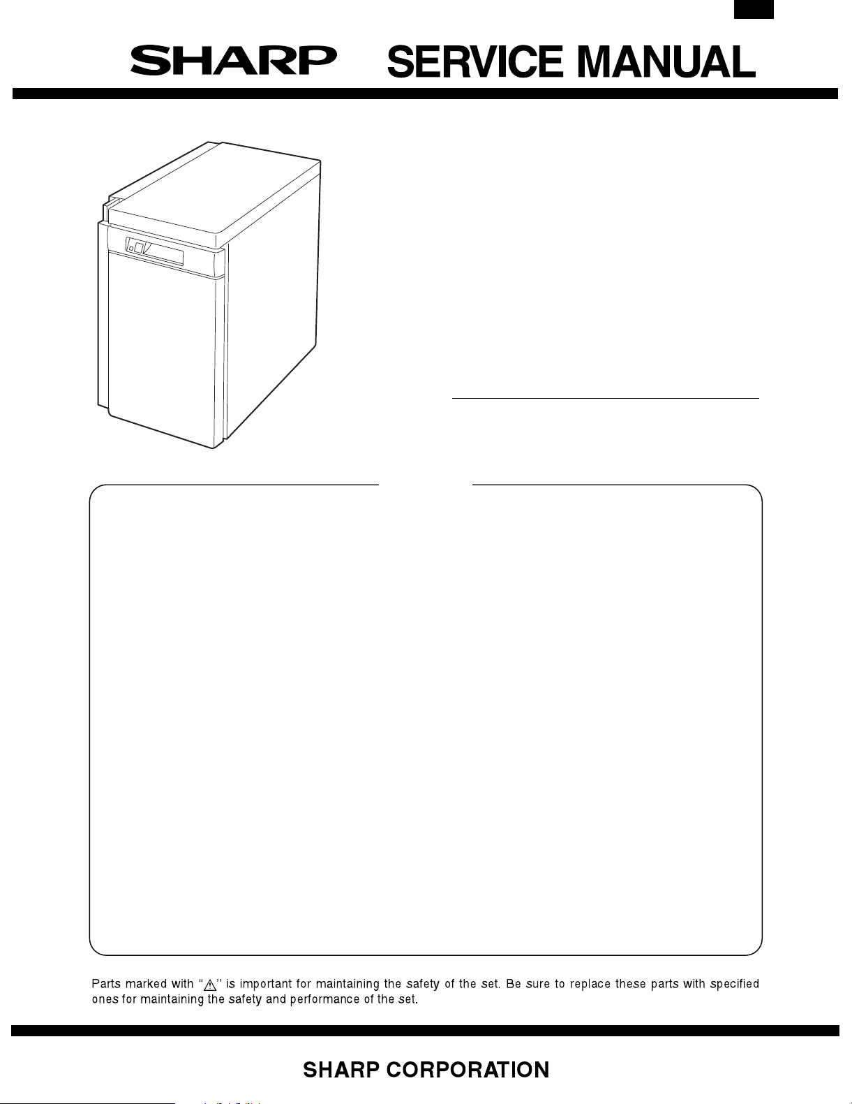
AR-LC1N
CODE: 00ZARLC1N/A1E
DIGITAL COPIER OPTION
LARGE-CAPACITY
PAPER FEED TRAY
MODEL AR-LC1N
CONTENTS
[Note]
This Service Manual describes only the differences from 00ZARLC1//A1E.
The items which are not described in this Manual are common with the
00ZARLC1//A1E.
[ 1 ] OUTLINE OF THE PRODUCT . . . . . . . . . . . . . . . . . . . . . . . . . . . . . . . 1-1
[ 2 ] SPECIFICATIONS . . . . . . . . . . . . . . . . . . . . . . . . . . . . . . . . . . . . . . . . 1-1
[ 3 ] UNPACKING AND INSTALLATION . . . . . . . . . . . . . . . . . . . . . . . . . . . 3-1
[ 4 ] EXTERNAL VIEW AND INTERNAL CONSTRUCTION . . . . . . . . . . . . 4-1
[ 5 ] OPERATING PRINCIPLE . . . . . . . . . . . . . . . . . . . . . . . . . . . . . . . . . . . 5-1
[ 6 ] DISASSEMBLY AND REINSTALLATION . . . . . . . . . . . . . . . . . . . . . . 6-1
[ 7 ] ADJUSTMENT . . . . . . . . . . . . . . . . . . . . . . . . . . . . . . . . . . . . . . . . . . . 7-1
[ 8 ] MAINTENANCE . . . . . . . . . . . . . . . . . . . . . . . . . . . . . . . . . . . . . . . . . . 8-1
[ 9 ] TROUBLESHOOTING . . . . . . . . . . . . . . . . . . . . . . . . . . . . . . . . . . . . . 9-1
[10] WIRING DIAGRAM . . . . . . . . . . . . . . . . . . . . . . . . . . . . . . . . . . . . . . . 10-1
[11] CIRCUIT DESCRIPTIONS . . . . . . . . . . . . . . . . . . . . . . . . . . . . . . . . . 11-1
PARTS GUIDE
This document has been published to be used
for after sales service only.
The contents are subject to change without notice.
Page 2

AR-LC1N
List of different points between the AR-LC1N and the AR-LC1
No.
Page Item Content Change Remark
1 1-1 [2]-9 Max. power consumption
about 17.6 W
2 11-1 [11] CIRCUIT DESCRIPTIONS Entirely changed. Refer to the
AR-LC1 AR-LC1N
Max. power consumption
Changed to about 25 W
attached page.
8/6/1999 – 1 –
Page 3
[11] CIRCUIT DESCRIPTIONS
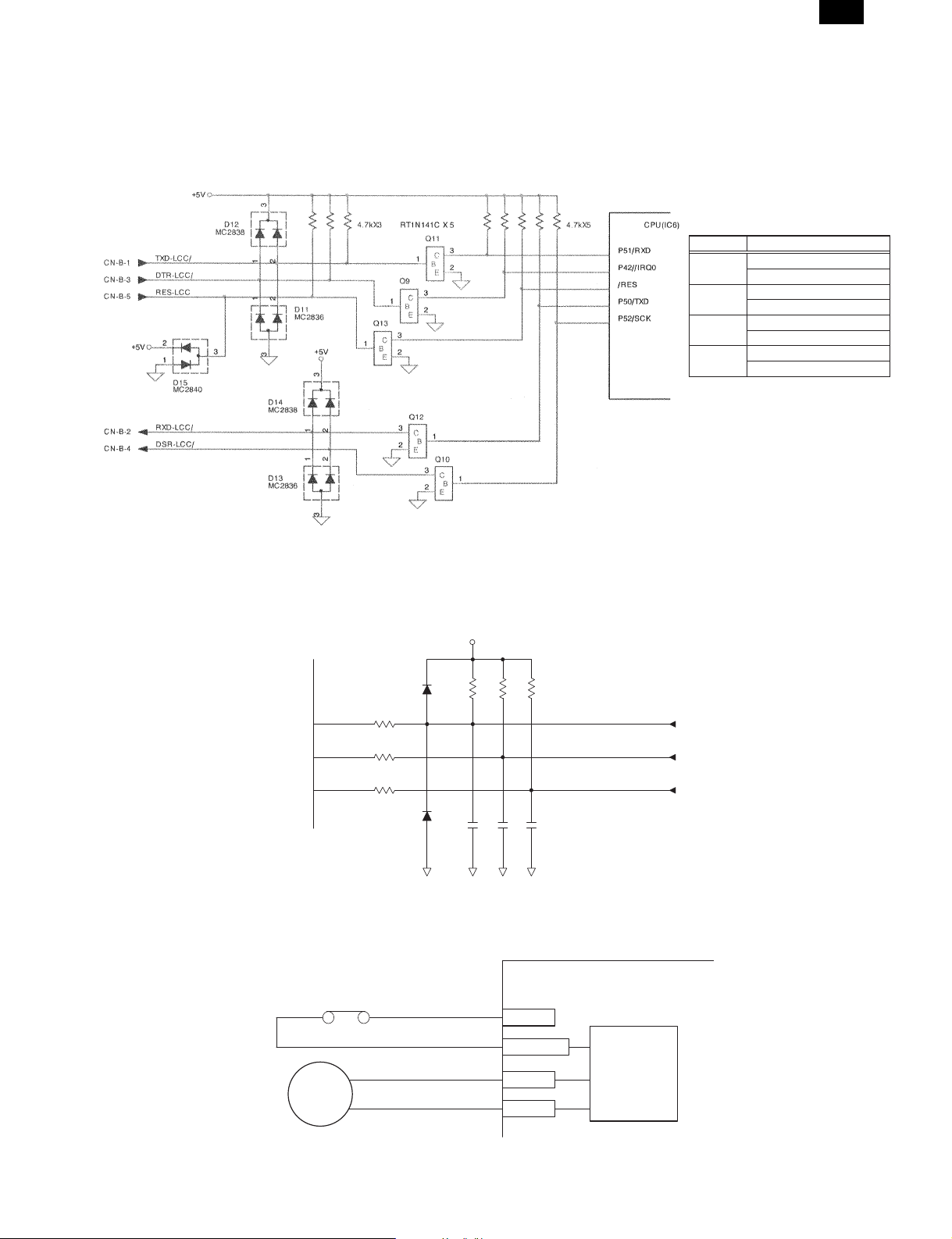
1. Operation
(1) Communication buffer circuit
On the communication buffer circuit, signals are input and output by the transistor RT1N141C (Q9 – Q13).
AR-LC1N
Signal name Logic
DSR-LCC
DTR-LCC
TXD-LCC
RXD-LCC
H: Request for communication
L: No request for communication
H: Communication allowed
L: Communication inhibited
H: Normal
L: Start bit
H: Normal
L: Start bit
(2) Sensor input circuit
The sensor signals used by the LCC are connected directly to the input port of the IC6. LPFD and LCD are provided with a static electricity noise
protective diode which protects against static electricity from the paper transport section. The other sensors have the same circuit configuration as the
LPED.
+5V
CPU
(IC6)
P74/AN4
P73/AN3
P76/AN6
18 LPFD
17 LDD
21 LPED
MC2838
10K
10K
10K
MC2836
D9
D10
R16
R15
22K
22K
C12 C11 C10
BR1
4.7K
1000P x 3
LPFD
LDD
LPED
CN-A-17
CN-A-23
CN-A-12
(3) Upper limit switch
A limit switch is provided to protect the LCC If it fails to operate normally. If the tray exceeds the upper limit sensor (LUD) position, the switch is turned
off to shut off the power of the lift motor.
LCC control PWB
Upper limit switch
24V
Lift motor
24V(LLSW)
Lift motor
LLM+
LLM-
drive circuit
11 – 1 8/6/1999
Page 4

AR-LC1N
(4) Solenoid and clutch drive circuit
The solenoids and clutches are driven by a Darlington transistor array M63823P with 7-circuit clamp diode. LPFS is turned on wh en the CPU’s port
output is at H. LPFC has the same circuit.
IC2
M63823P
+24V
SOL
CPU(IC6)
P66/FTOB
/TMRI1
29 LPFS
10.5K
7.2K
3K
LPFS/
CN-A-8
(5) Lift motor drive circuit
The tray height is adjusted according to the size of the paper mounted on the paper feed tray. The lift motor controls the rotational direction
(CW/CCW) with the control signals (LLMU, LLMD) from the CPU. The circuit forms a bridge circuit with STA457C to allow the CW/CCW control.
A fuse (F1) is provided to protect the motor against shorting or overload.
1-E4
LLMU
LLMD
1-E4
Lift motor
Forward rotation (UP)
Forward rotation (DOWN)
IC2
314
IC2
413
CPU port
LLMD LLMU
L
H
L
H
L
LOFF
R21 1K
R22 1K
IC3
7
2
R20 1K
1
R18
1K
6
D3
D2
1SS133x2
STA457C
2
7
3
3
1
8
8
4
4
9
9
6
5
51010
R17
10K
R19
10K
F1
1.25A/120V
T1.0A/250V
R3
3.9K
(1/4W)
C13
0.1uF
LLM+
LLM-
+24V(LLSW)
CN-A-3
CN-A-4
Suppose that both LLMD and LLMU become H level at the above circuit. If LLMU becomes H first, t he STA457C pin 3 become H, IC04 pin 13
through IC07 pin 6 become H due to diode D20. Even if LLMU is at H and LLMD at H on the port, STA457C pin 1 is at L and pin 6 at H, thus no
conduction of STA457C is achieved.
(6) Transport motor drive circuit
U
V
W
HU
HV
HW
RE\
The motor drive circuit is composed of IC4 motor ICs (Q5 – 8 (transistor), IC2 and IC5). When the PWM signal output from the CPU made at H level,
the transistor inside the IC5 turns on to supply current to the motor to start the motor. As the motor is started, hole signals (Hu, Hv, Hw) in side the
motor switch the input of IC4, while the output switches the transistor inside IC5. The motor thus starts rotating under non-control state.
When the motor rotates, the speed si gnal (RE) is output from the motor. The signal is taken into the CPU. If the motor speed is slow, the RWM signal
On duty is increased to increase the speed; if the motor speed is high, the PWM signal On duty is decreased to maintain the required speed.
As the current flowing to the mot or becomes large, the input voltage at the minus side of the IC7 rises. If the voltage exceeds the plus-side input
voltage, output voltage at IC7 becomes at L level, leading in the PWM signal to t urn off the transistor of Q5 so t hat the current to the motor is cut of f.
(setting: 3A).
8/6/1999 11 – 2
Page 5

AR-LC1N
(7) 24V power detection line
The line monitors 24V power. If the 24V power fed from the copier is not 24V, the level becomes L and the 24V power error is sent to the copier.
24V
R11
22K
14
P70/AN0
R10
4.7K
(8) Cassette detection line
This line has the same circuit as each sensor. When the LCC cassette door is opened, the CPU level becomes H when the door is closed, the line is
connected to GND and the CPU level becomes L.
5V
5V
P26/A14
33
10K
(9) LED lighting circuit
This is the LED lighting circuit for the cassette door switch.
R7
4.7K
1000p
D9
MC2838
D10
MC2836
Drawer connector
When the CPU outputs the L signal, the LED comes on.
11 – 3 8/6/1999
Page 6

AR-LC1N
D
1/3
CN-A-15
LPFD
1
R2
220(1/4W)
BR4
10kX4
12
8
7567586
BR5
10kX4
44
2
1
33
+5V
2
IC1
1
8
2
7
3
3
R31
22k
65
4
BR8
10kX4
4
324
1
BR9
4.7kX4
R26
4.7k
758
6
5
24
A16
2
OE
D0
D1
D2
D3
D4
D5
D6
D7
LTRC
LRE
DTR-LCC
A15
3
A15
A16
IC6
A14
29
21
D7D5D3
A11
A12A2A10
A13
23
25
4
28
A11
A12
A13
A14
D4
D5
D6
D7
17
18
19
20
D6
D4
49
50
51
52
53
54
55
56
57
58
59
60
61
62
63
64
H8/3294FP-64A
C
CN-A-6
LPFC/
BR6
10kX4
11
22
33
44
75867586
BR7
10kX4
A5
A3
A7
A4
A6A0A8
A9
A1
12
11
10
9
8
7
6
5
27
26
A10
D3
15
D2
A9
D2
P30/D0
P31/D1
P32/D2
P33/D3
P34/D4
P35/D5
P36/D6
P37/D7
P45//AS
A8
D1
14
D1
P41//IRQ1
P42//IRQ0
P43//RD
P44//WR
P46/CLK
P47//WAIT
13
D0
A7
D0
A0
48
1
RXD-LCC
A6
32
VCC(+5V)
A1
47
P10/A0
P50/TXD
2
TXD-LCC
A1
A2
A3
A4
A5
CE
PGM
VPP
VCC
1
30
22
31
C7
0.1u
4
1
2
3
BR11
10kX4
A6
A5
A4
A3
A2
42
43
44
45
46
P15/A5
P14/A4
P13/A3
P12/A2
P11/A1
P40//ADTRG//IRG
VCC
/NMI
/RES
P52/SCK
P51/RXD
7
6
5
4
3
VCC(+5V)
RES-LCC
/NMI
DSR-LCC
/STBY
A0
GND
NC
16
VSS(SGND)
5867
A7
VSS(SGND)
40
41
P17/A7
P16/A6
VSS
/STBY
9
8
VSS(SGND)
XTAL
VSS
XTAL
27C010
A8
39
10
EXTAL
A9
38
P20/A8
EXTAL
11
MD1
P21/A9
MD1
A10
37
12
MD0
A12
A11
A13
35
36
P23/A11
P22/A10
AVSS
MD0
14
13
/24VM
VSS(SGND)
34
P25/A13
P24/A12
P71/AN1
P70/AN0
15
/LDSW
A14
33
16
LCD
P26/A14
P72/AN2
IC2B
32
P27/A15
31
VCC
30
P67/TMO1
29
P66/FTOB/TMRI1
28
P65/FTID/TMCI1
27
P64/FTIC/TMO0
26
P63/FTIB/TMRI0
25
P62/FTIA
24
P61/FTOA
23
P60/FTCI/TMCI0
22
AVCC
21
P77/AN7
20
P76/AN6
19
P75/AN5
18
P74/AN4
17
P73/AN3
15
2
LPFC
M63823P
A15
VCC(+5V)
LPFC
LPFS
LLED/
PWM/
DIR
RE
LLMU
LLMD
VCC(+5V)
LPED
LUD
LTOD
LPFD
LDD
B
CN-A-17
CN-A-23
22k
22k
2
1
BR1
4.7kX4
7586
R7
4.7k
LPFD
LPED
8
BR2
10kX4
2
CN-A-12
LDD
LPFD
LPED
2134
LDD
/LDSW
LTOD
LUD
LCD
657
758
6
314
2
431
CN-A-29
CN-A-8
LPFS/
LLED
IC2A
M63823P
1 16
LPFS
R1
220(1/4W)
R8
4.7k
C
R9
4.7k
2-C2
2-B2
2-B2
DIR
PWM/RELLMU
B
2-C2
+5V
R15
+5V
R16
D9
MC2838
3
+5V
E
10k
Q4
DTD114GK
2-C2
LLMD
A
CN-A-11
CN-A-18
CN-A-28
CN-A-27
LCD
LUD
LTOD
/LDSW
C5
C8C9 C6
1000pX7
C10C11
C12
2
3
1
D10
MC2836
R10
4.7k
1
2
3
R11
22k
+24V
/24VM
BR3
10kX4
4
5
6
Q14
RT1N141C
C
E
7
8
B
7586
4.7kX4
BR13
3
+5V
D12
MC2838
2. LCC MAIN PWB
4.7k
R32
C14
0.1u
R42
4.7k
BR12
4.7kX4
1
34
2
75 86
C22
1000p
C21
0.1u
Q13
Q11
E
RES-LCC/
CN-B-5
RT1N141C
B
0.1u
C25
0.1u
C24
2
3
1
D11
MC2836
Q9
RT1N141C
C
B
C
4
213
2
1
DTR-LCC/
TXD-LCC/
LRE/
CN-B-3
CN-B-1
CN-A-24
RT1N141C
E
C
E
B
3
D15
MC2840
1
2
D
+
C1
47u/35V
Q12
RT1N141C
C
D14
MC2838
2
3
+5V
1
RXD-LCC/
DSR-LCC/
CN-B-4
CN-B-2
C
R14
0J(JUMPER)
R13
10K
CPUMODESELLECTP ART
R12 10k
X1
8.00MHz
B
E
B
C
Q10
RT1N141C
D13
MC2836
2
3
1
or
+5V
0J(JUMPER)
L1
ACB20120M-150-T
VCC(+5V)
VSS(SGND)
L2
or
CN-A-5
CN-A-7
CN-A-1
0J(JUMPER)
ACB20120M-150-T
+24V
E
+24V
+24V
CN-B-09
CN-A-9
CN-A-10
+5V
C33
0.1u
C3
47u/35V
+
GND
JP1
GND1
CN-B-10
CN-A-16
+5V
CN-A-21
+5V
CN-B-7
C32
+
C4
CN-A-22
CPUMODESELLECTP ART
CN-C-1
0.1u
47u/35V
GND2
CN-B-8
B
INTER-ROM
0EUPWB0409
N31,32,41,42
OUTER-ROM
UNITCODE
CN-A-14
CN-A-13
CN-B-6
A
H
MODE(MODE3)
H
MODE(MODE1)
MD0
(12Pin)
CPU
CPUMODE
CN-A-19
CN-A-20
H
L
MD1
(11Pin)
PORT
LOGIC
CN-A-25
+24V(LLSW)
+24V(LLSW)
CN-A-2
R13
ASSEN-
CN-A-26
R14
BLE
PARTS
CN-C-6
6
7
8
8/6/1999 11 – 4
Page 7

AR-LC1N
D
C
B
A
2/3
1
+24V
C2
100U/35V
+
2
R33
R34
R43
3
4
CN-C-7
CN-C-8
CN-C-9
U
V
W
ISR124-400X3
0.1u
D6 D7 D8
10
7
3
1
OC
OB
OA
VCC
IA2
IB2
IC2
GND
GND
IC1
IB1
IA1
IC5
9
8
2
1k
1k
1k
2.2K
R25
R23 2.2K
R24 2.2K
12
M63823P
IC2E
5
Q8
RT1N141C
SLA6012
4
6
5
11
12
C18
C15
1k
R36
R35
R27
11
10
M63823P
IC2F
IC2G
6
7
Q7
RT1N141C
Q6
1k
1k
M63823P
RT1N141C
0.1uX3
R39 680
R38 680
R37 680
+10V
+5V
C19
C16
1
IC7A
BA10393
4
8
+
-
3
2
0.1u
C17
R30
2.4k
R28
Q5
200
RT1N141C
R40
R29
360
R4
0.22(1W)
C20
0.1u
10k
F1
IC2C
+24V(LLSW)
1.25A/120V
T1.0A/250V
IC3
STA457C
7
2
14
M63823P
3
CN-A-3
CN-A-4
LLM+
LLM-LLM-
0.1u
C13
R3
3.9k(1/4W)
R19
10k
9
4
8
3
8
3
7
2
1
1
1k
R20 1k
R22 1k
R21 1k
IC2D
R17
10k
9
4
10
10
5
5
6
6
R18
1SS133x2
D3
D2
13
M63823P
4
1
2
3
4
6
7
+10V
2.7k
R41
5
6
+5V
5
BR10
10kX4
234
9
7
16
15
14
13
12
11
GND
OUT1
OUT2
OUT4
OUT6
OUT3
OUT5
REVERSE
VREF
VCC
IN6
IN5
IN4
IN3
IN2
IN1
IC4
1
2
4
6
3
8
5
2.2kX4
4
3
21
10
+10V
2.2k
R45
2.2k
R44
+5V
BR14
876
5
7
7
6
5
BR15
1.2kX4
4
3
2
8
UPC1246C
0.1u
C23
C27 C29
C28 C26
R46
1000pX4
1-D2
PWM
LLMU
1-D2
LLMD
1-D2
1-D2
DIR
7
IC7B
BA10393
+
-
5
6
5
6
RE
1-D2
10k
R5
1k(1/4W)
+24V
FR1
100(1/4W)
R6
1k(1/4W)
Q1
2SC1472K
+10V
IC2
9
+24V
D5
RD18FB1
C30
0.1u
C31
0.1u
D4
RD11EB
8
7
8
LCC MAIN PWB
D
RE/
HWHVHU
CN-C-5
CN-C-2
CN-C-3
C
CN-C-4
B
A
11 – 5 8/6/1999
Page 8

AR-LC1N
D
C
B
A
3/3
1
2
3
1
2
3
4
5
6
7
8
9
1
2
3
CN-C(B9B-EH-A)
5V
RE/
HU
HV
HW
GND2
U
V
W
4
RXD-LCC
GND2
DSR-LCC
GND1
GND2
5
12
34
56
78
910
TXD-LCC
5V
RES-LCC
DTR-LCC
CN-B(B10B-PHDSS-B)
24V
6
24V(LLSW)
LLM-
LPFC/
LPFS/
5V(LPED)
LPED
GND2(LPED)
5V(LTOD)
LTOD
GND2(LTOD)
5V(LRE)
LRE/
GND2(LRE)
LCD
N.C.
2
4
6
87
12
14
109
1615
18
1
3
5
11
13
7
17
24
2019
28
21 22
23
27
29 30
25 26
4
5
6
7
24V(OUT)
LLM+
24V(LPFS)
5V(LUD)
LUD
GND2(LUD)
5V(LPFD)
LPFD
GND2(LPFD)
5V(LDD)
LDD
GND2(LDD)
/LDSW
CN-A(B30B-PHDSS-B)
24V(LPFC)
LLED
8
LCC MAIN PWB
D
8/6/1999 11 – 6
C
8
B
A
Page 9

CAUTION FOR BATTERY REPLACEMENT
(Danish) ADVARSEL !
Lithiumbatteri – Eksplosionsfare ved fejlagtig håndtering.
Udskiftning må kun ske med batteri
af samme fabrikat og type.
Levér det brugte batteri tilbage til leverandoren.
(English) Caution !
Danger of explosion if battery is incorrectly replaced.
Replace only with the same or equivalent type
recommended by the manufacturer.
Dispose of used batteries according to manufacturer’s instructions.
(Finnish) VAROITUS
Paristo voi räjähtää, jos se on virheellisesti asennettu.
Vaihda paristo ainoastaan laitevalmistajan suosittelemaan
tyyppiin. Hävitä käytetty paristo valmistajan ohjeiden
mukaisesti.
(French) ATTENTION
Il y a danger d’explosion s’ il y a remplacement incorrect
de la batterie. Remplacer uniquement avec une batterie du
même type ou d’un type équivalent recommandé par
le constructeur.
Mettre au rebut les batteries usagées conformément aux
instructions du fabricant.
(Swedish) VARNING
Explosionsfara vid felaktigt batteribyte.
Använd samma batterityp eller en ekvivalent
typ som rekommenderas av apparattillverkaren.
Kassera använt batteri enligt fabrikantens
instruktion.
AR-LC1N
Page 10

AR-LC1N
All rights reserved.
Printed in Japan.
No part of this publication may be reproduced,
stored in a retrieval system, or transmitted,
in any form or by any means,
electronic; mechanical; photocopying; recording or otherwise
without prior written permission of the publisher.
SHARP CORPORATION
Digital Document Systems Group
Quality & Reliability Control Center
Yamatokoriyama, Nara 639-1186, Japan
1999 August Printed in Japan
 Loading...