

Page 1

SERVICE MANUAL
Digital copier option
Staple sorter
MODEL AR-FN5
CONTENTS
[ 1 ] SPECIFICATIONS ............ ............................ .............................. ............ 1
[ 2 ] UNPACKING AND INSTALLATION ....................................................... 2
[ 3 ] EXTERNAL VIEW AND INTERNAL STRUCTURE................................ 5
[ 4 ] OPERATIONAL DESCRIPTIONS ........ .................................................. 8
[ 5 ] DISASSEMBLY AND SSEMBLY ........ .................................... .............. 13
[ 6 ] ADJUSTMENTS ................................................................................... 20
[ 7 ] MAINTENANCE............ .................. .................. .................. .................. 22
[ 8 ] TROUBLESHOOTING.......................................................................... 23
[ 9 ] CIRCUIT DESCRIPTIONS ........... .................... ...................... .............. 25
[10] OUTLINE MAP ............................................................... ...................... 35
[11] ELECTRICAL SECTION....................................................................... 36
Parts marked with " " are important for maintaining the safety of the set. Be sure to replace these parts with specified
ones for maintaining the safety and performance of the set.
This document has been published to be used
SHARP CORPORATION
for after sales service only.
The contents are subject to change without notice.
Page 2

[1] SPECIFICATIONS
1. Type
Installation-to-the-copier type
2. Tray
Number of trays: 2
Type: Upper tray, normal type
Lower tray, lift-up type (with the offset function)
Capacity: Upper tray, 100 pages
Lower tray, 1,000 pages (500 pages for A4/Letter
or greater)
3. Paper transport
Center reference
4. Paper exit syst e m
Face down
5. Paper exit size
9. Paper exit job
Machine tray: Printer, FAX, and copy output
Finisher upper tray: FAX output and interruption output
Note: The factory default is 1. Setup to 2, 3, 4 is made
by the user.
When a COPY/FAX model is set to the default
(1), an interrupt copy to the top tray is inhibited.
Finisher lower tray: Copy, printer output
10. Staple secti on
Staple allowed: Lower tray
Binding capacity: M ax. 30 pages (80g/u or less)
Paper size: AB series: A3, B4, A4, A4R, B5
Inch series: 11x17, 8.5x14, 8.5x13, 8.5x11, 8.5x11R
For Mainland China: A3, B4, A4, A4R, B5, 16k, 8k
Binding reference: Parallel binding at one position
Staple supply: Cartridge-type (3,000 pcs. or more)
Detection: Staple empty detection, no cartridge detec-
tion
Manual stapling: Not provided.
Upper tray: A4 / A4R / A5 / A5R / B4 / B5 / B5R / A5 / 11x17 /
8.5x14 / 8.5x13 / 8.5x11 / 8.5x11R / INV / FC / OHP /
Label sheet / Second original / 16k / 16kR / 8k
Lower tray: A3 / A4 / A4R / B4 / B5 / B5R / 11x17 / 8.5x14 / 8.5x13 /
8.5x11 / 8.5x11R / FC / 16k / 16kR / 8k
6. Paper weight
52 ~ 128g/m2 (Upper/lower trays)
7. Paper exit full detection
Provided (Upper/lower trays)
8. Offset
Offset allowed: Lower tray
Offset quantity: 27mm
1 1. Power source
Supplied from the copier. 24V/5V/3.3V
12. Power consumption
63W (Max.)
13. External dimensions
Finisher paper exit section: 173.5(W) x 511(D) x 540(H) mm (Except
for the tray)
Compiler section: 562(W) x 444(D) x 109(H) mm
14. Weight
About 19kg (Finisher body 11kg, compiler section 7kg)
Note: The finisher cannot be used with the manual paper feed tray.
Page 3

[2] UNPACKING AND INSTALLATION
1. Unpacking
2. Installation
If this unit is installed together with AR-SP4/RP3 or DM-SP2/RP1,
install AR-SP4/RP3 or DM-SP2/RP1 before installing this unit.
For improvement of workability, part of the description in this manual
may be modified without prior notice. In this case, refer to the service
manual.
Turn off the main switch of the co pi er an d the n r emove
the power plug of the copier from the outlet.
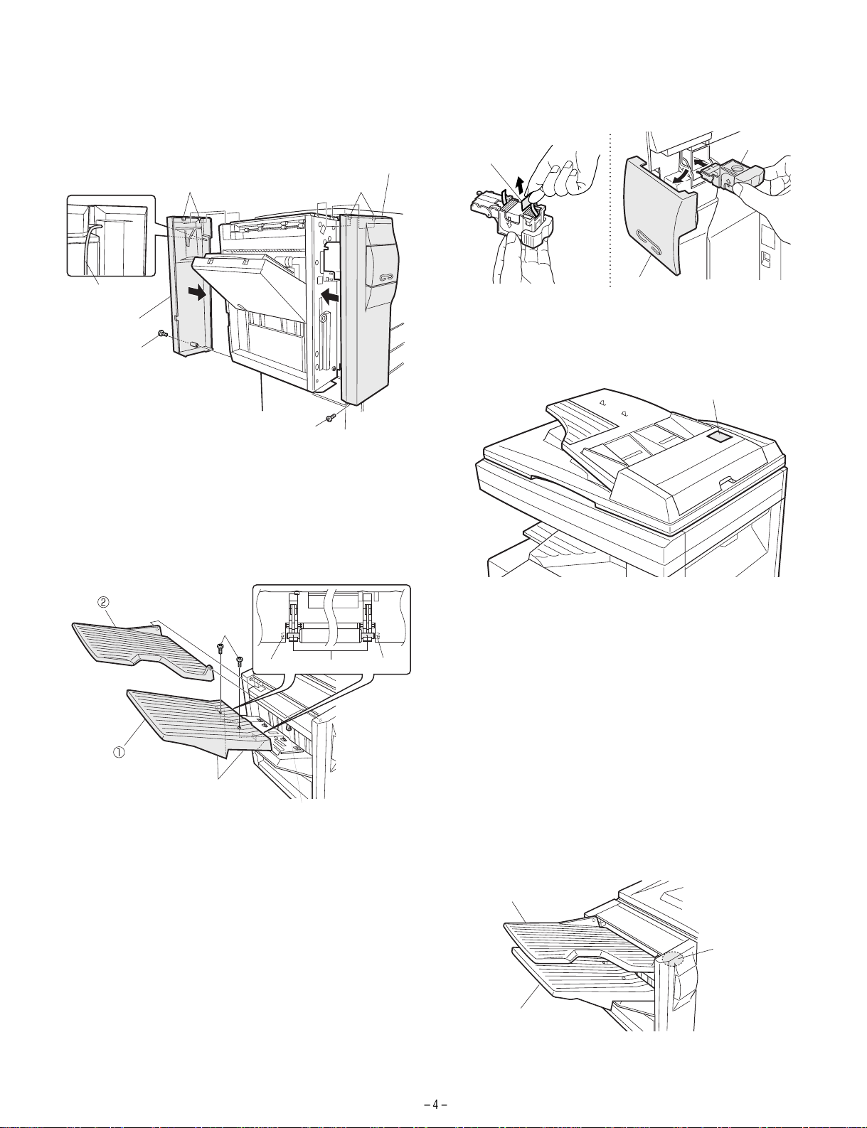
1. Remove the inner cabinet from the copier.
< 1 > Pull the lock lever to the right and then pull out the rail dummy
cover to remove it.
<2> Remove the pawl from the exit dummy cover and remove the exit
dummy cover.
Lock lever
Rail dummy cover
Pawl
Exit dummy cover
<3> Remove the screw and remove the rear exit cover.
<4> If this unit is installed together with AR-SP4/RP3 or DM-
SP2/RP1, install AR-SP4/ RP3 or DM-SP2/RP1 before installi ng
this unit.
Top tray: 1 pc.
Harness cover: 1 pc.
Screws (M4 x 10): 10 pcs.
Offset tray unit: 1 pc.
Staple cartridge: 1 pc.
Mounting fixtures: 2 pcs.
Staple position label
: 1 sheet
Installation manual
: 1 sheet
Remove all pieces of fixing tape and fixing materials from
the finisher.
· < 1 >, to < 2 >, < 3 >, < 4 >, < 5 >, < 7 >, and < 8 > indicate tape.
· < 6 >, < 9 >, and < 10 > indicate fixing material.
Paper pressure rollers
Rear exit cover
Screw (M3 x 10)
2. Fit the mounting fix ture s.
Cut and remove the two cut-out portions from the right cabinet of the
copier using a tool such as nippers.
(Be careful about the direction of the tool so that the cut surface is
flat.)
Fix the two mounting fixtures using two screws (M4 x 10) respectively.
Cut-out portions
Screws (M4 x 10)
Tape (wire handling)
Tape
Metal fitting
Screws (M4 x 10)
Metal fitting
Page 4

3. Remove the front and rear cabinets.
Remove the screw for each cabinet and remove the front and rear
cabinets.
Rear cabinet
Screw (M4 x 10)
Screw (M4 x 10)
Front cabinet
4. Attach the exit unit.
Lower the exit unit from above the mounting fixtures so that the right
and left positioning bosses are placed into the U-shaped grooves of
the fixtures. Then, fix the front side and the rear side using a screw
(M4 x 10) respectively.
5. Attach the alignment unit.
Place the rails of the alignment unit on the guide of the copier and
push it until it stops. Then, attach it using two screws (M4 x 10).
Guide
Rail
Harness
Pass the harness here.
Copier guide
Alignment unit
Screw (M4 x 10)
Right rail of
alignment unit
Screw (M4 x 10)
6. Connect each connector
< 1 > Connect the two harnesses of the alignment unit and the stapl e
connector to the exit unit relay harness on the front side.
< 2 > Pull out the harnesses of the alignment unit through the hole of
the copier rear frame and connect them to the three connectors
of the finisher PWB.
Front side Rear side
Rear side
Bosses
Mounting fixtures
U-shaped groove
U-shaped groove
<3> Connect the harness to the connector of the copier and fix it
using the screws.
Screws
Harness
7. Attach the harn es s co ve r .
Insert the rib of the harness cover into the left inner cabinet and then
hang the pawl on the right frame.
Screw (M4 x 10)
(Top view)
Screw (M4 x 10)
Rib
Pawl
Harness cover
Page 5
8. Attach the front and rear cabinets.
After hanging the ribs of the front and rear covers on the frames,
attach the front and rear cabinets using a screw (M4 x 10) respectively.
At this time, paste the connection harness to the rear cabinet as
shown in the illustration.
Front cabinet
Ribs
Ribs
10. Mount the staple cartridge.
Remove protective paper from the cartridge.
Open the staple cover, insert the staple cartridge to the staple unit
until it clicks, and then close the staple cover.
Staple cartridge
Protective paper
Connection
harness
Rear cabinet
Screw (M4 x 10)
Screw (M4 x 10)
9. Attach the trays.
< 1> Raise the paper holder lever, insert the two pawls on the rear
side of the offset tray unit to the mounting positions, and fix the
tray using the two screws (M4 x 10).
< 2> Insert the bosses of the escape exit tray into the mounting holes
shown in the illustration and attach the tray.
Top tray
Screw
(M4 x 10)
Roller shaft
Offset tray unit
pawls
Paper holder lever
[CAUTION]
When attaching the offset tray, make sure that part of the roller shaft
of the offset tray is not on the offset tray.
NGNG
Staple cover
11. Paste the staple po si tio n la be l.
Paste the staple position label to the document feeder.
staple position label
Insert the power plug of the copier to the outlet and turn
on the main switch of the copier. Then, carry out the
following procedure.
12. Check for stapl in g op er a tio n.
Make three copies in the staple sort mode.
Check to see if stapling has been performed properly.
13. Check for paper delivery to the top tray.
Deliver two copies to the top tray.
If this equipment is installed together with a printer expansion kit or a
facsimile expansion kit, check the appendix of each operation manual
(key operator programs and index list output and setting).
14. Check for paper delivery to the offs et tray .
Deliver three sets from two originals to the offset tray.
Check to see if copies have been offset stacked properly.
Escape exit tray
Offset tray
Installation of staple sorter is now complete.
Stapling position
Page 6

[3] EXTERNAL VIEW AND INTERNAL STRUCTURE
1. External view
1
2
3
No. Name
1 Upper tray
2 Lower tray
3 Alignment unit
Page 7
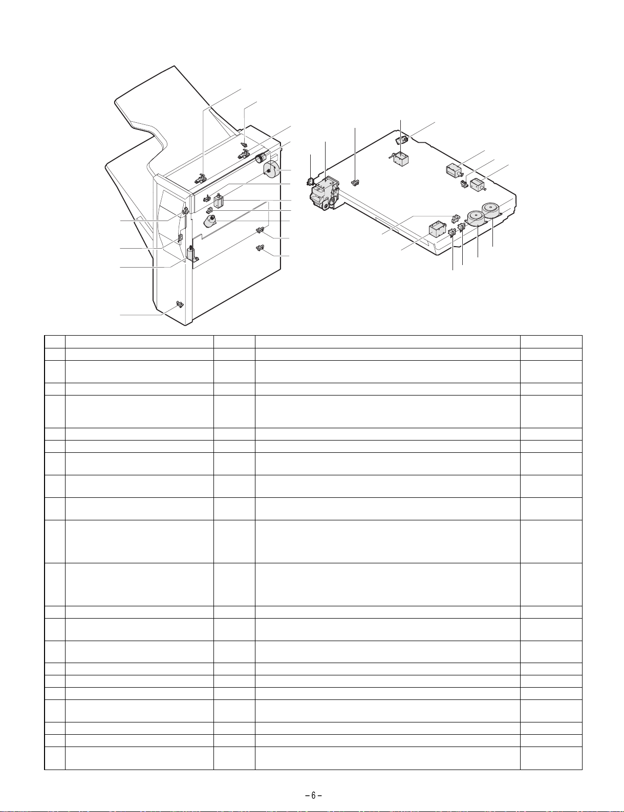
2. Sensors, motors, solenoids, etc.
1
2
3
4
29
17
16
5
6
7
8
18
12
13
9
10
11
28
27
14
15
No. Part name Code Function/Operation Type
1 Upper tray paper exit sensor T10D Counts down the output page, detects JAM. Photo sensor
2 JAM process PG open/close detection
switch
3 Escape full sensor T1PD Detects paper full in the upper stage tray (ESC tray). Photo sensor
4 Paper exit roller rotation control clutch ORCLD Used to select whether to slow the speed of the paper exit roller upper
5 Main drive motor FMM Drives the rollers for paper transport. Pulse motor
6 Lower tray paper exit sensor /T20D Counts down the output page, detects JAM. Photo sensor
7 Paper hold solenoid OFSLD Presses paper onto the paper shift prevention lever of the lower stage
8 Paper position sensor /T2PD Detects the top surface of discharged paper, and detects the upper
9 Tray offset drive motor OFM
10 Tray position sensor (Upper) T2UP Detects the lift-up tray position in combination with the tray position
11 Tray position sensor (Lower) T2DN Detects the lift-up tray position in combination with the tray position
12 Offset home position sensor OFHP Detects the standby position of the offset tray. Photo sensor
13 Staple supply cover open/close
detection switch
14 Lift-up motor LUM
15 Lift-up drive control sensor LUEN Reads the encoder for control of the DC motor rotation. Photo sensor
16 Stapler unit
17 Tray paper empty sensor ATPD Detects paper presence or empty on the alignment tray. Photo sensor
18 Shutter drive solenoid STSLD When discharging a bundle of paper, shift the lead edge reference
19 Upper alignment plate drive solenoid AJSLD Holds paper on the alignment tray. Solenoid
20 Side guide plate home position sensor SDHP Detects the home position of the width alignment members. Photo sensor
21 Transport switch gate solenoid Right GRSLD Drive to sort paper into the escape transport section and the alignment
TCSW Interlocks when the open/close PG of the transport section in front of
(+, –)
SCSW Detects the staple supply cover open/close. When open, interlocks. Micro switch
(+, –)
the upper stage tray is open.
for the speed of the paper exit roller lower or to make it as a normal
follower roller.
tray upper.
standby position of the lift-up tray.
Supplies drive power to separate paper and shift the tray to the front
and the rear.
sensor (lower). (Upper limit detection in the case of erroneous detection
by the paper position sensor, intermediate position detection, and full
detection)
sensor (upper). (Upper limit detection in the case of erroneous
detection by the paper position sensor, intermediate position detection,
and full detection)
Drives the lift-up tray up and down. DC motor
plate in the paper transport direction.
tray.
22
26
25
24
19
23
20
21
Micro switch
Electromagnetic
clutch
Solenoid
Photo sensor
DC motor
Photo sensor
Photo sensor
Solenoid
Solenoid
Page 8
No. Part name Code Function/Operation Type
22 Transport switch gate solenoid Left GLSL Drive to sort paper into the escape paper exit port and the li ft -up tray
paper exit port.
23 Side guide plate alignment motor SDM Aligns paper vertically to the paper transport direction. Pulse motor
24 Reciprocating alignment motor BKM Aligns paper in the paper transport direction. Pulse motor
25 Paper entry sensor INPD Detects paper entry in the finisher and detects JAM. Switch trigger of
the transport switch gate right.
26 Paper width sensor WDPD Make a distinction between A4 and A5R, LT and INVR. If the paper
entry sensor is ON and this sensor is OFF, it is A5R or INVR.
27 Rear edge plate drive solenoid BKSLD Drives the rear edge plate. Solenoid
28 Rear edge plate home position sensor BKHP Detects the home position of the rear edge alignment members. Photo sensor
29 Tray JAM process detection switch PGSW Interlocks when the alignment tray is opened downward in a JAM
process.
Solenoid
Photo sensor
Photo sensor
Micro switch
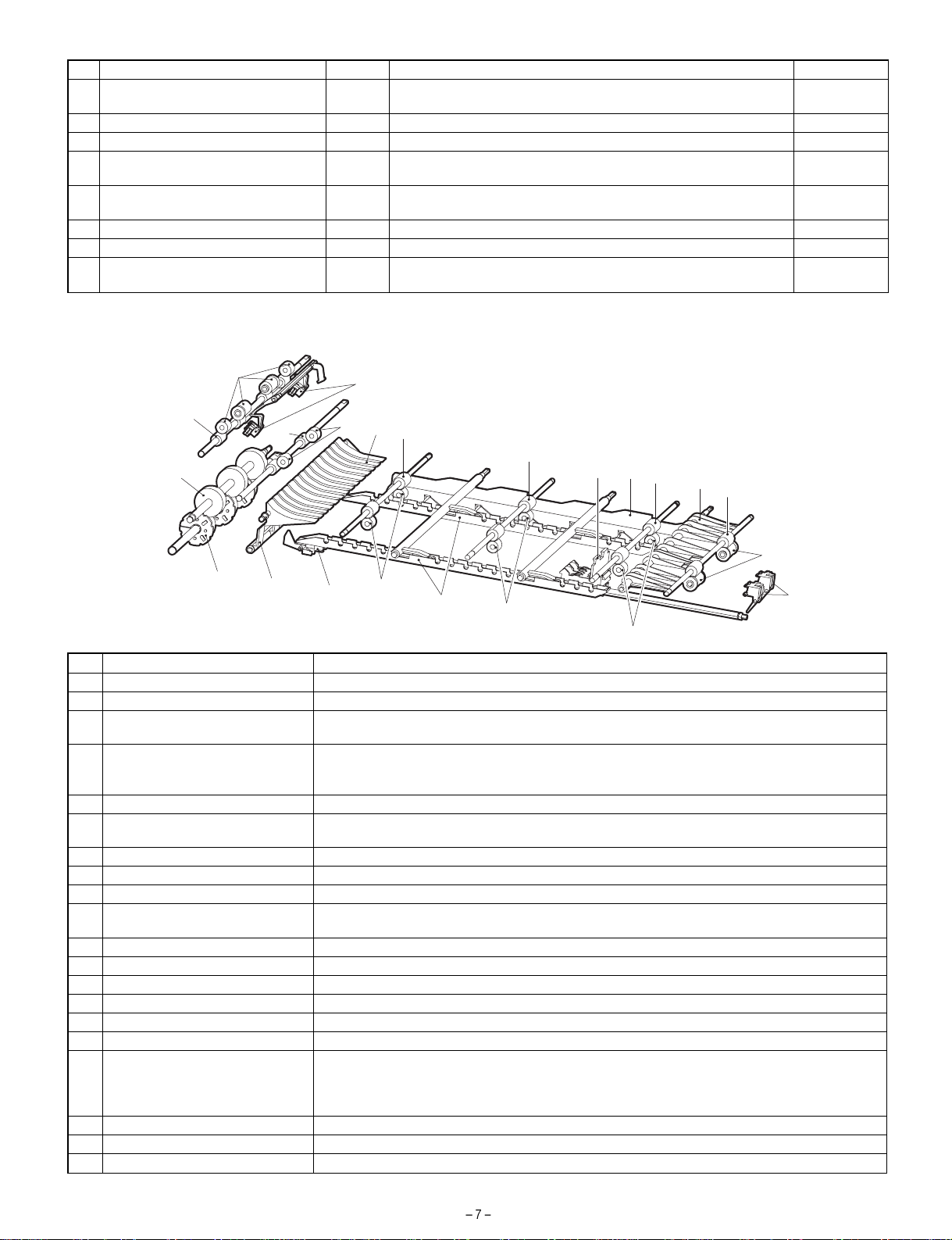
3. Rollers, gates, etc.
15
16
13
17
12
14
11
19
2
7
5
2
4
20
3
18
10
9
8
6
8
1
8
No. Name Function
1 Paper entry sensor Detects paper transported from the machine.
2 Transport roller fin Transports paper in combination with No. 8 roller.
3 Paper entry follower roller (Kick-out
sponge)
4 Transport switch gate right Selects between the escape transport (non-staple mode) and the alignment tray transport (staple
5 Side guide plate Aligns paper vertically to the paper transport direction.
6 Upper alignment hold plate Knocks paper when paper (5th page or later) comes on the alignment tray removing air or adjusting
7 Rear edge plate Aligns paper in the paper transport direction.
8 PS upper roller (Common part) Transports paper in combination with No. 2, 19, 20 rol lers.
9 Paper empty sensor (1A71A) Detects paper empty on the alignment tray.
10 Shutter Serves as the paper lead edge reference for alignment of paper, and opens to allow a bundle of
11 Transport switch gate left Selects between the escape tray transport and the offset tray transport.
12 PS upper roller (Common part) Transports paper in combination with No. 13 roller.
13 Escape transport roller Transports paper in combination with No. 12 (No. 8) roller.
14 Escape paper exit sensor Detects paper transport to the escape tray.
15 Transports paper in combination with No. 16 roller.
16 Escape paper exit roller Transports paper in combination with No. 15 roller.
17 Paper exit roller upper Transports paper in combination with No. 18 roller. This roll er normally follows No. 18 roller. When
18 Paper exit roller lower Transports (discharges) paper in combi nation with No. 17 roller.
19 Transport drive roller fin Transports paper in combination with No. 8 roller.
20 Paper entry roller fin Transports paper in combination with No. 8 roller.
Transports paper in combination with No. 2 roller.
mode).
When selecting the alignment transport (staple mode), this gate drops t he rear edge of paper.
curls.
paper to be transported to the paper exit port after stapling.
discharging a stapled bundle of paper, the electromagnetic clutch turns on to make this roller a drive
roller. The bundle of paper is bent by the difference between thi s roller speed and the No. 18 roller
speed so that it is not caught by the preceding bundle staple.
Page 9

[4] OPERATIONAL DESCRIPTIONS
1. Paper transport path
a. Tray 1 paper exit
b. Tray 2 paper exit (Offset function selectable)
c. Tray 2 staple paper exit
3. Paper exit of a stapled bundle
·
In the case of A3, WL
a. When paper is discharged from t he machine, the finisher raises
the direction switch gate right to pass the paper to the alignment
tray. When the read edge of paper passes the paper entry sensor,
the operation is triggered. That is, when the rear edge of paper
passes the direction switch gate right, the gate i s lowered to store
the rear edge of paper completely in the alignment tray.
2. Operational descriptions
1. Paper exit to the top tray
When paper is discharged from the machine, the finisher lowers the
direction switch gate right to pass the paper to the upper transport
path (escape transport section) and lowers the direction switch gate
left to discharge the paper to the top tray. The direction switch gate
right is triggered by the finisher paper entry sensor and operated only
when the paper lead edge passes through it.
2. Paper exit to the offset tray
When paper is discharged from the machine, the finisher lowers the
direction switch gate right to pass the paper to the upper transport
path, and lowers the direction switch gate left to discharge the paper
to the offset tray. The direction switch gate right is triggered by the
finisher paper entry sensor and operated only when the paper lead
edge passes through it.
b. The rear edge plate and the side guide plate are moved in the
paper alignment direction to lower the upper alignment plate, performing alignment. After alignment, stapling is performed by the
staple unit.
c. After alignment and stapling, the side guide plate is loosened and
the shutter is lowered to discharge paper to the paper exit roller by
the rear edge plate. The bundle of paper is discharged to the offset
tray by the paper exit roller.
· In the case of small size
a. The rear edge plate is moved to the center and the direction switch
gate right is raises to pass the paper to the alignment tray. When
the read edge of paper passes the paper entry sensor, the operation is triggered. That is, when the rear edge of paper passes the
direction switch gate right, the gate is lowered to store the rear
edge of paper completely in the alignment tray.
Page 10

b. When the second last paper is passed, the rear edge plate (1) is
lowered and passed under the paper bundle (2) to the rear edge of
the paper bundle (3). Then the rear edge plate is raised. (HP
position)
e. The rear edge plate and the side guide plate are moved in the
paper guiding direction and the upper guide plate is lowered to
perform the last alignment. Then stapling is performed by the staple unit.
f. After alignment and stapling by the stapler unit, the side guide
plate is loosened and the shutter is lowered. The paper is moved
to the paper exit roller by the rear edge plate, and discharged to
the offset tray by the paper exit roller.
(1) (2) (3)
c. When the last paper from the machine passes the direction switch
gate right, it lowers the gate.
d. The paper bundle is moved in the paper exit direction by the rear
edge plate.
3. Descriptions on each section
This machine is composed of the paper exit unit and the alignment
unit. The paper exit unit includes the paper exit tray 1 and 2. The
paper exit tray 2 is provided with the offset function and the lift-up
function.
The alignment unit includes the paper transport section used f or the
non-staple mode, the paper alignment section for the staple mode,
and the staple unit.
a. Paper exit unit section
(1) Paper transport (Main motor)
By rotating the main drive motor, the paper exit unit and the all transport rollers of the alignment unit are driven.
(2) Tray 1 full detection
The top of paper bundle on the tray is detected by t he combination of
the lever and the photo sensor to judge paper full on Tray 1.
(3) Lift-up section
· Lift-up motor
In order to discharge paper always at a fixed posi tion regardl ess of
paper load on the tray 2, the lift-up motor is driven, the pulley is
rotated normally or in reverse, and the timing belt is driven to move
the tray 2 up and down.
Page 11
· Full detection
Paper full on the tray 2 is detected in combination between the
lower limit sensor ON and detection of the top of paper bundle on
the tray by the paper exit actuator.
(4) Offset tray section
· Offset motor
The offset motor moves the offset tray vertically to the paper exit
direction so that each bundle of paper discharged to the offset tray
is separately grouped.
· Paper exit clutch
This clutch is turned on when a stapled bundle of paper is discharged so that the bundle of paper is warped by the difference
between the speeds of the upper and the lower paper exit rollers,
preventing the bundle from being caught by the preceding bundle’s
staple.
b. Alignment unit section
(1) Transport switch gate right (gate right solenoid)
Selection between the transport section and the alignment section
in the alignment unit is made by the transport switch gate right.
This gate drops the rear edge of paper entering the alignment
section so that the rear edge is completely transported.
(2) Rear edge plate uni t
· Rear edge plate motor
The motor is turned on at the timing when paper enters the alignment tray to drive the rear edge plate unit. Paper of A3 or WLT is
aligned to the shutter, and paper of a smaller size is aligned to the
right side of the alignment tray in the transport direction.
· Rear edge plate solenoid
After provisional alignment of small size paper, this solenoid puts
down the rear edge plate of the rear edge unit to pass it under the
aligned paper. After returning to the home position, it is turned off
and the rear edge plate is put back and paper is transported to the
shutter.
(3) Side guide plate (Guide plate motor)
When paper enters the alignment tray, this plate is driven to align
paper vertically to the paper transport direction toward the fixed
wall of the alignment tray front side.
(4) Shutter (Shutter soleno id )
The shutter solenoid drives the shutter which stops the lead edge
of paper for alignment. After stapling, the shutter is put down to
transport paper to the paper exit roller.
(5) Transport switch gate left (Gate left solenoid)
Paper passed through the escape transport path is sent to the tray
1 or to the tray 2.
4. Basic operations
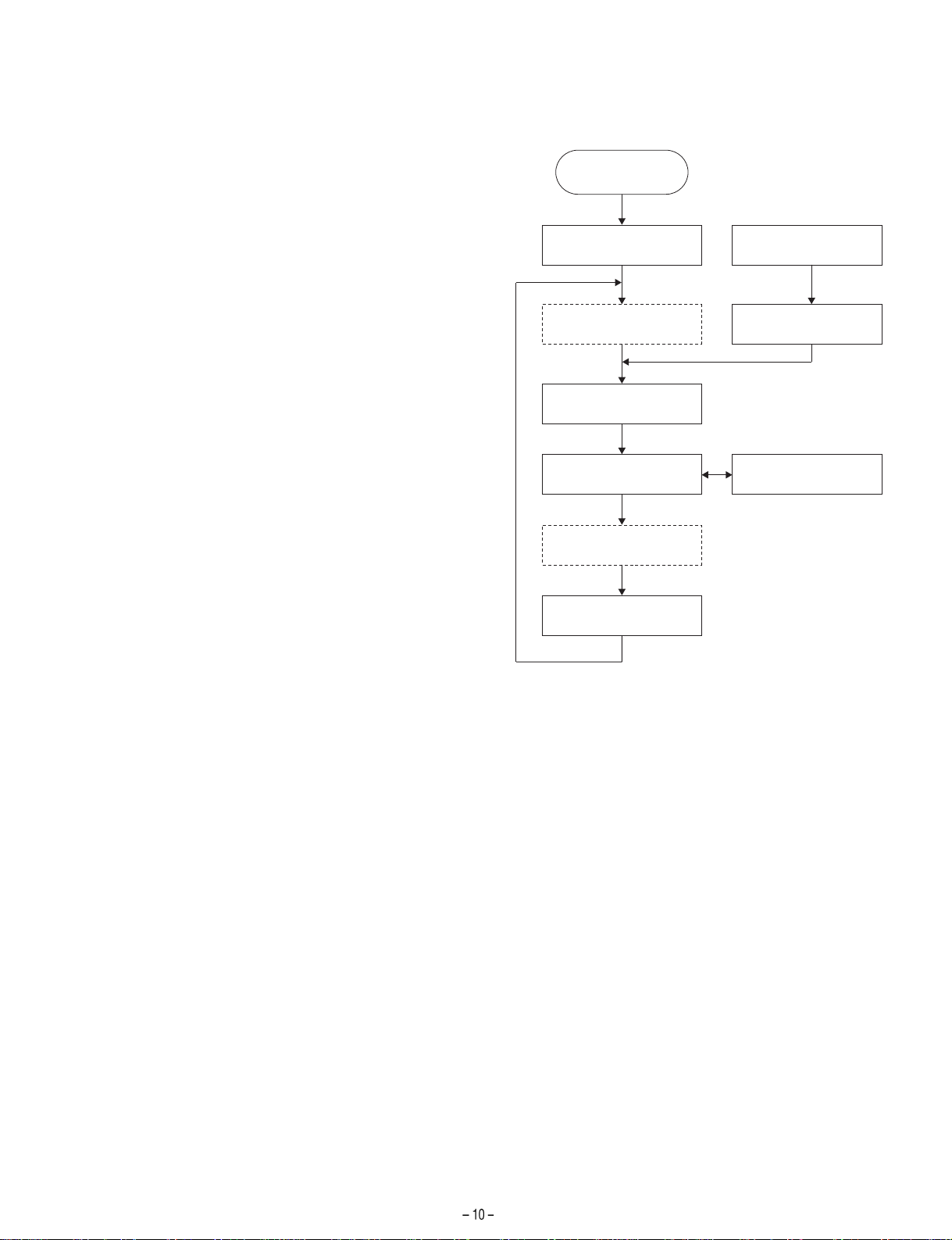
A. Flowchart of basic operations
Power ON
Initializing at power ON
Individual printing
operation (Offset tray)
Job start operation
Transport operation
Offset paper exit operation
Job end operation
The initialization (home positioning of each motor) is performed at the
following timing:
1) When the power is turned on.
2) When the staple section door on the upper side of the finisher
paper exit unit is opened or closed.
3) When the alignment unit is opened or closed.
4) When the copy start key is pressed (JOB_START): Recovery operation
5) When copying is completed (JOB_END).
6) When a jam occurs: Jogger saving
Operation in case
of an error
Operation when the
door is closed
Stapling operation
Page 12
B. Operations of each section when the power it turned on
Unit No. Operation Remark
Alignment unit Escape transport upper unit 1 Finisher paper entry detection OP: Paper provided. JAM display
CL: Paper empty. Go to READY
2 Paper width detection
3 Transport switch gate right drive
4 Transport switch gate left drive
Escape transport lower unit 5 Upper alignment plate drive
Alignment tray unit 6 Side guide plate alignment drive
7 Rear edge plate alignment drive
8 Rear edge plate drive
9 Side guide plate home position
10 Rear edge plate unit home position
11 Shutter drive
12 Tray paper empty detection
Staple unit 13 Staple empty detection
14 Cartridge empty detection
15 Stapling operation
16 Home position detection
17 Self priming
Others 18 Staple supply cover open/close detection
19 Tray JAM process detection
Paper exit tray unit Escape tray 20 No. 1 tray paper exit detection
21 JAM process PG open/close detection
Lift-up tray 22 No. 2 tray paper exit detection
23 Lift-up drive
24 Lift-up drive rotation control
25 Tray position detection (upper)
26 Paper position detection
27 Tray position detection (lower)
28 Tray offset drive
29 Offset home position
Main drive system 30 Main rotation drive
31 Paper exit roller rotation control
5. Operational specifications of each section
(1) Operational specifications of side guide plate
Pulse motor specifications and control
· 1 step = 7.5 degrees
· 1-2 phase drive 1200pps
· Reduction ratio 15P ® 40P = 24P (MXL tooth shape)
· Side guide plate shift for an input of 1 pulse: 0.1905mm / pulse
· Slow up/down control for tuning:
Basic operations of side guide plate
1. Moving to the standby position
· The side guide plate is moved from the home position to the
standby position according to the paper size information supplied
by the main body.
Paper width (mm) Shift quantity (mm) Pulse number (pluse)
A3, A4 297 0 0
B4, B5 257 22.1 116
A4R 210 45.5 239
WLT, LT 279.4 12.4 65
RG, LTR,GLG 215.9 42.7 224
Page 13
· The pulse number is rounded at the first digit below the decimal
point.
2. Alignment operation start
· Alignment operation is started at timer control after the paper
entry sensor is turned OFF.
¯
Timer time = 59.6(mm) / 122(mm/s) + a = About 0.7
3. Shift quantity in alignment
Paper width (mm) Shift quantity (mm) Pulse number (pluse)
A3, A4 297 27.4 144
B4, B5 257 45.3 238
A4R 210 69.0 362
WLT, LT 279.4 32.0 168
RG, LTR,GLG 215.9 65.9 346
· The pulse number is rounded at the first digit below the decimal
point.
4. Alignment operation
· Reciprocating operations in the above shift quantity are per-
formed. At the last page, the plate stops at a position about 2mm
from the edge. ® Staple process
¯
The last return is made by the pushing quantity (2).
· For provisonal alignment paper (B4 or less), the rear edge plate
passes under a bundle of paper to reach the home position, and
stands by at a position slightly wider than the paper width (about
2mm) until the final alignment is performed toward the shutter.
After completion of the final alignment, the plate stops at a position about 2mm from the edge similarly to the above, and stapling
is performed.
5. Paper exit operation
· When a bundle of paper is discharged after stapling, the side
guide plate moves to a position so as not to interfere discharging
and to prevent against skew feeding of the bundle.
¯
Paper width 12pulse (about 2.3mm)
6. Next job
· The rear edge plate pushes paper by specified distance, and
returns to the home position. The above procedures are repeated
for the next job.
· If the operation is completed wi th one job, the plate ret urns to the
home position.
(2) Operational descriptions of rear edge plate
Pulse motor specifications and control
· 1 step = 7.5 degrees
· 1-2 phase drive 847pps (600pps when discharging a paper bun-
dle)
· Reduction ratio 15P ® 20P = 26P
· Side guide plate shift for an input of 1 pulse: 0.141275mm / pulse
· Slow up/down control for tuning
Basic operations of side guide plate
1. Moving to the standby position
The side guide plate is moved from the home position to the
standby position according to the paper size information supplied
by the main body.
The standby position and the alignment operations differ depending on the following two size groups:
A3, WLT
B4, LG, FC, A 4 , B5, A4R, LT, LTR
Paper width (mm) Shift quantity (mm) Pulse number (pluse)
WLT 431.8 24.8 60
A3 420 24.8 60
B4 384 395.0 957
RG 355.6 393.8 954
GLG 330.2 368.6 893
A4R 297 335.2 812
LTR 279.4 317.8 770
LT 215.9 254.3 616
A4 210 248.5 602
B5 182 220.4 534
2. Alignment operation start
Alignment operation is started at timer control after the paper
entry sensor is turned OFF.
¯
Timer time = 59.6(mm) / 122(mm/s) + a = About 0.7
3. Shift quantity in alignment
Paper width (mm) Shift quantity (mm) Pulse number (pluse)
WLT 431.8 9.9 24
A3 420 20.6 50
B4 384 1.7 4
RG 355.6 7.4 18
GLG 330.2 8.3 20
A4R 297 8.3 20
LTR 279.4 8.3 20
LT 215.9 8.3 20
A4 210 8.3 20
B5 182 8.3 20
· The pulse number is rounded at the first digit below the decimal
point.
4. Alignment operation
· A3, WLT
Reciprocating alignment operation in the above shift quantity is
performed toward the shutter. At the last page, the plate stops at a
position about 2mm from the edge. ® Stapling process
· B4 or less
Reciprocating alignment operation in the above shift quantity is
performed toward the provisional alignment reference wall. After
the last page is aligned, the rear edge is put down, and t he unit
returns to the home position. After detection of the home position,
the rear edge plate is raised and the bundle of paper is transported
to the shutter. After completion of the final page alignment, the
plate stops at the paper edge. ® Stapling process
5. Paper exit operation
The stapled bundle of paper is lifted up by the rear edge plate and
pushed to the paper exit roller.
6. Next job
· The pushing distance of a paper bundle is a little bit greater than
the distance (71.6mm) between the shutter and the paper exit
roller. After pushing, moves toward the home position without
putting down the rear edge plate. The next job paper which is in
stand-by in front of PS is fed, and the above procedures are
repeated.
If the operation is completed with one job, the paper bundle is
Page 14

discharged and the plate returns to the home position.
[5] DISASSEMBLY AND ASSEMBLY
(3) Paper size detection
1. Body Paper-In sensor
Detects the paper size by the ON time.
¯
The following sizes cannot be judged only with the length.
A4 and A5R
A5 and postcard
LT and INVR
Some kinds of envelopes
2. Width detection of paper before discharging from the body
· No. 1 tray (escape tray) output inhibition size
¯
Postcards, envelopes
· No. 2 tray (list-up tray) output inhibition size
¯
A5, A5R, INV. INVR, postcards, envelopes
· Staple inhibition size
¯
B5R, above uncertain sizes
For disassembly, follow the sequence of the illustration numbers. For
assembly, reverse the disassembly procedures.
For disassembly and assembly of parts which are not described in this
manual, refer to the Parts Guide.
1. Finisher
A. Alignment plate unit
1-A-1
2)
4)
3)
1)
1-A-2
1-A-3
1-A-4
1)
3)
2)
4)
2)
1)
3)
Page 15

1-A-5
1)
B. Paper exit unit
1) Remove the alignment unit.
1)
2)
3. Paper exit unit and each roller
Move down the offset tray unit to the bottom, and remove the paper
exit unit from the copier.
Then remove the rollers from the paper exit unit.
Procedures to move down the offset tray unit to the bottom
2)
1)
1-B-1
1-B-2
3)
When turning on the power, lift the paper holding lever which
detects the top of the tray with your fingers.
When the tray reaches the bottom, turn off the power. (When
the lever moves about half of the moving distance, you may
release your fingers, and the tray will fall to the bottom.)
3-1
2. Stapler unit
1) Remove the alignment unit.
2-1
3-2
1)
2)
Page 16

3-3
1)
3-7
2)
3-4
3-5
2)
1)
3)
2)
3-8
1)
1)
1)
2)
2)
3)
3-6
1)
1)
1)
1)
2)
1)
3-9
3-10
2)
3)
2)
1)
1)
2)
Page 17

3-11
2)
A. ESC paper exit roller
B. ESC transport roller
C. Upper paper exit roller
3-A-1
1)
2)
3-12
3-13
2)
2)
1)
1)
2)
3)
3)
1)
2)
2)
2)
3-A-2
1)
3-A-3
1)
5)
2)
2)
2)
1)
1)
3)
3)
2)
1)
4)
3-A-4
1)
1)
2)
3)
4)
4)
1)
2)
3)
Page 18

4. Paper exit unit motor
A. Main drive motor
4-A-1
C. Lift-up motor
Note: Perform this procedure after removing the right cabinet (Step
3-5).
Refer to Fig.(3-1) to (3-6).
4-C-1
4-A-2
2)
1)
3)
4)
2)
1)
3)
4-C-2
1)
3)
1)
2)
3)
2)
1)
B. Offset tray drive motor
Refer to Fig.(3-1) to (3-4).
2)
4-B-1
3)
1)
5. Paper exit unit solenoid
Refer to Fig.(3-1) to (3-6).
5-1
1)
2)
3)
Page 19

5-2
2)
6-2
3)
1)
2)
1)
3)
4)
2)
5-3
1)
6. Alignment unit roller
6-1
2)
1)
6-3
6-4
1)
2)
2)
1)
3)
4)
6)
5)
4)
Page 20

7. Alignment unit motor
Refer to Fig.(6-1) to (6-2).
7-1
7-4
1)
3)
1)
7-2
1)
1)
1)
2)
2)
3)
3)
2)
4)
4)
5)
5)
8. Alignment unit sol enoid
Refer to Fig.(7-1) to (7-2).
A. Upper alignment plate drive solenoid
8-1
1)
7-3
1)
2)
1)
2)
B. Transport switch gate solenoid right
8-2
2)
2)
1)
Page 21

C. Rear edge plate solenoid
Refer to Fig.(7-3).
1)
8-3
2)
8-4
3)
5)
[6] ADJUSTMENTS
Adjustments are required when replacing the following parts:
A. Rear edge plate unit
B. Side guide plate
C. Gate solenoid right
4)
2)
D. Gate solenoid left
E. Upper alignment solenoid
F. Shutter solenoid
G. Rear edge plate solenoid
H. Paper holding solenoid
A. Rear edge plate unit
1. Staple 5 sheets of A4 or LT paper, and check the slide shift of the
paper bundle in the transport direction (Y-axis).
2. When the shift of the paper bundle is within 1mm, there is no need
to adjust.
3. If the shift of the paper bundle is greater than 1mm, execute SIM
3-6-3 to adjust the rear edge plate position.
D. Shutter drive solenoid
Refer to Fig.(7-3).
8-5
2)
3)
E. Transport switch gate solenoid
Refer to Fig.(1-A-1) to (1-A-5).
Refer to Fig.(6-1) to (6-2).
8-7
2)
1)
B. Side guide plate
1. Staple 5 sheets of A4 or LT paper, and check the slide shift of the
paper bundle in the vertical direction (X-axis) to the transport direction.
2. When the shift of the paper bundle is within 1mm, there is no need
to adjust.
4)
1)
1)
3. If the shift of the paper bundle is greater than 1mm, execute SIM
3-6-2 to adjust the side guide plate position. Also check that the
paper bundle is in parallel with the alignment reference wall of the
side guide plate.
SIM 3-6 Finisher alignment member adjustment
(Initial screen)
Sim3-6 JOGGER ADJ.
1:PAPER SIZE
2:JOGGER POS X
3:JOGGER POS Y
1
When a sub code is entered, the above display is shown.
1. In SIM 3-6-1, press [OK] and select [1] - [10] to specify the paper
size.
2. Enter SIM 3-6-2 Jogger pos X (side guide plate) or SIM 3-6-3
Jogger pos Y (rear edge plate) and press [OK]. The alignment
section (rear edge plate unit), side guide plate) will be operated.
During the load operation, the [OK] key is highlighted.
3. Keep the alignment member at the paper alignment position, and
open the alignment section. Insert paper of the sam e size into the
alignment member and check that the tightness is proper. 1~2 mm
smaller (tight) than the paper size is O.K.
4. When the adjustment value of the simulation is decreased by 1,
the clearance between paper and the side guide plate is decreased by 0.41mm, and between paper and the rear edge plate
0.83mm, and vice versa.
Page 22

C. Gate solenoid right
E. Upper alignment solenoid
Mark the solenoid installing position before replacement, and fix a new
one to the marked position.
After fixing, press the plunger with your finger to adjust so that the
lead edge of the gate right is in a position 16.5mm ~ 17mm apart from
the alignment tray transport surface. Release the finger and check
that it returns smoothly by the spring and that the lead edge of the
gate right is in a position 36mm apart from the transport surface.
36mm
Mark the solenoid installing position before replacement, and fix a new
one to the marked position.
After fixing, pull the plunger with your finger and check that the upper
alignment holding plate is in contact with the alignment tray. Then
release the finger and check that the plunger returns sm oothly by the
spring.
16.5 17
mm
D. Gate solenoid left
Mark the solenoid installing position before replacement, and fix a new
one to the marked position.
After fixing the solenoid, check and adjust so that the gate left edge is
in contact with the transport surface on the transport PG with the
plunger released, and so that the gate left edge is 6.5 - 7mm from the
transport surface.
F. Shutter solenoid
Mark the solenoid installing position before replacement, and fix a new
one to the marked position.
After fixing, pull the plunger with your finger and check that the shutt er
rotates 90 degrees and makes contact with the tray. Then release the
finger and check that the shutter returns smoothly by the spring and
that it is vertical to the alignment tray after returning.
O
90
6.5 7mm
Page 23

G. Rear edge plate solenoid
H. Paper holding solenoid
Mark the solenoid installing position before replacement, and fix a new
one to the marked position. (The solenoid and the installing plate
positions are determined by the round hole.)
After fixing, pull the plunger with your finger and check that the rear
edge plate rotates 90 degrees and makes contact with the rear edge
plate slide. Then release the finger and check that the rear edge plate
returns smoothly by the spring and that it is vertical to the alignment
tray after returning.
Fix the paper holding solenoid below the long fixing hole so that the
whole paper hold installing plate unit is in the lower limit of the adjustment range.
(The solenoid and the installing plate positions are determined by the
round hole.)
[7] MAINTENANCE
Note: Before maintenance, disconnect the power cable from the body.
Be sure to avoid communication during maintenance. It is very dangerous.
For maintenance, refer to the DISASSEMBLY AND ASSEMBLY and the Parts Guide.
The table below shows the maintenance parts and the work contents.
Part name Work content Condition of execution Cycle
Transport rollers Cleaning Maintenance/Servicing 40K or 2 years
Paper guides Cleaning Maintenance/Servicing 40K or 2 years
Gears Lubrication, greasing Maintenance/Servicing 40K or 2 years
Belts Check Maintenance/Servicing 80K or 2 years
Staple unit Replacement Maintenance/Servicing 200K (Number of operations)
Sensors Check Maintenance/Servicing 40K or 2 years
OF roller cleaner Cleaning Maintenance service When the lead edge or rear edge of paper is dirtied or at 20 - 25K
For maintenance of the OF roller cleaner, refer to the figure below.
Reference: 65 ~ 66 times of staple replacement
Page 24

[8] TROUBLESHOOTING
1. List
Trouble code
Main code Sub code
F1 00 Finisher communication trouble FIN
01 Finisher jogger shift trouble
06 Finisher shift motor abnormality
08 Finisher staple shift motor trouble
11 Pusher motor trouble
15 Finisher elevator motor trouble
Details of trouble Trouble detection
2. Selfdiagnostics
Trouble code
Main code Sub code
F1 00 Content Finisher communication trouble
Details Communication li ne test error occurs when power is turned on or after the exit of a simulation mode.
Cause Connection trouble or disconnection of the connector and harness between the body and the finisher.
Check and
remedy
01 Content Finisher jogger shift trouble
Details Jogger shift trouble
Cause Motor lock.
Check and
remedy
06 Content Finisher shift motor abnormality
Details Finisher shif t motor breakdown
Cause Motor lock
Check and
remedy
08 Content Finisher staple shift motor trouble
Details Staple motor drive trouble
Cause Motor lock.
Check and
remedy
11 Content Pusher motor trouble
Details Pusher motor trouble
Cause Motor lock
Check and
remedy
15 Content Finisher elevator motor trouble
Details Elevator motor trouble
Cause Motor lock.
Check and
remedy
Error in Finisher communication
Finisher control PWB trouble Control PWB failure Malfunction by noises
Turn off/of the power to cancel the trouble.
Check connector/harness of communication line
Replace the finisher control PWB.
Motor rpm abnormality
Overcurrent to motor
Finisher control PWB failure
Check the jogger motor operation with SIM 3-3.
Motor rpm abnormality
Overcurrent to motor
Finisher control PWB failure
Check the shift motor operation with SIM 3-31.
Motor rpm abnormality
Overcurrent to motor
Finisher control PWB failure
Check the operation of the staple motor with SIM 3-3.
Motor rpm abnormality
Overcurrent to motor
Finisher control PWB failure
Check the pusher motor operation with SIM 3-3.
Motor rpm abnormality
Overcurrent to motor
Finisher control PWB failure
Check the elevator motor operation with SIM 3-31.
Details of trouble
Page 25

3. Troubleshooting
1) Copier communication trouble (F1-00)
Check item Step Cause/Trouble position Result Remedy
Is the illustration of the finisher displayed on the LCD of
the operation panel?
Is the power supplied normally? (5V, 3.3V) 2 Machine OP interface PWB No Replace the OP interface PWB.
Does replacement of the finisher PWB cancel the trouble? 3 Finisher PWB Yes End
2) Paper exit unit trouble
2-1) Lift-up motor trouble (F1-15)
Check item Step Cause/Trouble position Result Remedy
Do the offset tray upper limit and lower limit sensors
respond correctly?
Does the paper hold sensor respond correctly? 2 Paper hold sensor No Replace the sensor(s). Check
Does the lift-up encoder respond correctly? 3 Lift-up encoder No Replace the sensor(s). Check
Is wiring between the finisher PWB and the lift-up motor
normal?
Does replacement of the offset motor cancel the trouble? 5 Lift-up motor No Replace the lift-up motor.
Does replacement of the finisher PWB cancel the trouble? 6 Finisher PWB Yes End
2-2) Offset motor trouble (F1-06)
Check item Step Cause/Trouble position Result Remedy
Does the offset tray home position sensor respond
normally?
Is the wiring between the finisher PWB and the offset
motor proper?
Does replacement of the offset motor cancel the trouble? 3 Offset motor No Replace the offset motor.
Does replacement of the finisher PWB cancel the trouble? 4 Finisher PWB Yes End
1 Machine connection cable No Replace the machine connection
cable.
1 Upper/lower limit sensors No Replace the sensor(s). Check
wiring.
the wiring.
wiring.
4 Wiring No Replace or repair the wiring.
1 Offset home position sensor No Replace the sensor. Check the
wiring.
2 Wiring No Replace or repair the wiring.
3) Alignment unit trouble
3-1) Side guide plate hom e po si tio n err o r (F1-0 1)
Check item Step Cause/Trouble position Result Remedy
Does the side guide plate position sensor respond
normally?
Is the wiring between the finisher PWB and the side guide
plate motor proper?
Does replacement of the side guide plate cancel the
trouble?
Does replacement of the finisher PWB cancel the trouble? 4 Finisher PWB Yes End
1 Side guide plate home position
sensor
2 Wiring No Replace or repair the wiring.
3 Side guide plate motor No Replace the side guide plate
No Replace the sensor. Check the
wiring.
motor.
3-2) Rear edge plate home position error (F1-11)
Check item Step Cause/Trouble position Result Remedy
Does the rear edge plate position sensor respond
normally?
Is the wiring between the finisher PWB and the rear edge
plate motor proper?
Does replacement of the rear edge plate motor cancel
the trouble?
Does replacement of the finisher PWB cancel the trouble? 4 Finisher PWB Yes End
1 Rear edge home position sensor No Replace the sensor. Check the
wiring.
2 Wiring No Replace or repair the wiring.
3 Rear edge plate motor No Replace the rear end plate
motor.
4) Staple motor error (F1-08)
Check item Step Cause/Trouble position Result Remedy
Does the home position sensor respond normally? 1 Staple unit No Replace the staple unit.
Is the wiring of the finisher staple unit proper? 2 Wiring No Replace or repair the wiring.
Does replacement of the staple unit cancel the trouble? 3 Staple unit No Replace the staple unit.
Dose replacement of the finisher PWB cancel the trouble? 4 Finisher PWB Yes End
Page 26

[9] CIRCUIT DESCRIPTIONS
1. General
The finisher main circuit sends/receives commands to/from the copier’s MCU PWB, and control s loads according to the commands and controls
input/output of sensor/switch information.
The finisher is composed of this circuit, the circuit which makes inputs from sensors and switches, the circuit which drives motors/solenoids/clutches,
ROM, RAM, and the peripheral circuits.
2. Block diagram
The finisher block diagram is shown below.
FINISHER BLOCK DIAGRAM
2TRAY FINISHER
COPIER
/FINCRDY
/FINSRDY
STAPLE SWITCH
CARTRIDGE SWITCH
P-IN SENSOR
PAPER WIDE SENSOR
TRAY1 P-OUT SENSOR
TRAY2 P-OUT SENSOR
STAPLE HP SENSOR
SELF PRIMING SENSOR
LIFT UP ENCODE
SIDE HP SENSOR
BACK HP SENSOR
TRAY2 UP SENSOR
TRAY2 DOWN SENSOR
ADJUST TRAY PAPER
SENSOR
PAPER POSITION SENSOR
(T2PD)
TRAY1 P-FULL SENSOR
OFFSET HP SENSOR
FINSTS
FINCMD
/RES
Reserved
/FINDET
GP1S44S1
GP1S44S1
GP1S44S1
GP1S44S1
GP1A71A
GP1A71A
GP1A71A
GP1A71A
GP1A71A
GP1A71A
GP1A71A
GP1A71A
GP1A71A
GP1A71A
GP1A71A
9.8304MHz
+24V
PS
+5V
+3.3V
S-GND
P-GND
BUFFER
LS244
BUFFER
LS244
H8S/2350
/CRDY
/SRDY
RxD
TxD
/RES
CPU
RAM
2K
A0~A16
D0~D15
RY/BY
/WE
/CE
/OE
(256K bit)
FLASH ROM
M29F200BA
DRIVER
MTD1361
DRIVER
MTD1361
DRIVER
MTD1361
DRIVER
DRIVER
TA7291P
DRIVER
TA7291P
DRIVER
TD62318
DRIVER
TD62318
Level
switch
circuit
SRAM
+24V
PULSE
MAIN MOTOR
MOTOR
BACK BOARD
PULSE
MOTOR
PULSE
MOTOR
DC
MOTOR
DC
MOTOR
DC
MOTOR
SL
SL
SL
SL
SL
CL
SL
MOTOR
SIDE CONTROL
STAPLER MOTOR
LIFT UP MOTOR
OFFSET MOTOR
GATE-L SOLENOID
ADJUST SOLENOID
SHUTTER SOLENOID
GATE-R SOLENOID
BACK BOARD
SOLENOID
P-OUT CLUTCH
PAPER HOLD
SOLENOID
STAPLER COVER
SWITCH
PG COVER SWITCH
MOTOR
SW24
+5V
TRAY COVER SWITCH
Page 27

3. CPU (H8S/2350)
3.1. General
The CPU controls the finisher loads and controls the system by sending/receiving commands to/from the machine MCU PWB through the
serial communication line.
3.2. Features
The H8S/2350 is a microcomputer based on the H8S/2000 CPU, in
which the peripheral functions required for the system are integrated.
The H8S/2000 CPU is of internal 32bit composition, and is equipped
with the general-purpose registers of 16bit x 16 and the simple, optimized command set with high-speed operations. It can handle 16MB
linear address space.
Its major functions include the DMA controller (DMAC), the bus master of the data transfer controller (DTC), RAM, memory, the 16bit timer
pulse unit (TPU), the programmable pulse generator (PPG), the watch
dog timer (WDT), the serial communication interface (SCI), the A/D
converter, the D/A converter, the I/O port, and other peripheral functions.
3.3. Pin configuration
AVCC
VREF
P40/AN0
P41/AN1
P42/AN2
P43/AN3
P44/AN4
P45/AN5
P46/AN6/DA0
P47/AN7/DA1
AVSS
VSS
P17/PO15/TIOCB2/TCLKD
P16/PO14/TIOCA2
P15/PO13/TIOCB1/TCLKC
P14/PO12/TIOCA1
P13/PO11/TIOCD0/TCLKB
P12/PO10/TIOCC0/TCLKA
P11/PO9/TIOCB0/DACK1
P10/PO8/TIOCA0/DACK0
MD0
MD1
MD2
PG0/CAS
PG1/CS3
PG2/CS2
φ
P52
P51
P53/ADTRG
102
101
103
104
105
106
107
108
109
110
111
112
113
114
115
116
117
118
119
120
121
122
123
124
125
126
127
128
12345678910111213141516171819202122232425262728293031323334353637
P50
PF2/LCAS/WAIT/BREQ0
PF1/BACK
VSS
VSS
9998976995949392919089888786858483828180797877767574737271706968676665
100
PF3/LWR
PF0/BREQ
PF4/HWR
PF5/RD
PF6/AS
PF7/
EXTAL
VSS
XTAL
VCC
VCC
STBY
NMI
WDTOVF
RES
P21/PO1/TIOCB3
P20/PO0/TIOCA3
P27/PO7/TIOCB5
P26/PO6/TIOCA5
P25/PO5/TIOCB4
P24/PO4/TIOCA4
P23/PO3/TIOCD3
P22/PO2/TIOCC3
P63/TEND1
P62/DREQ1
VSS
VSS
P60/DREQ0/CS4
P61/TEND0/CS5
VSS
38
64
63
62
61
60
59
58
57
56
55
54
53
52
51
50
49
48
47
46
45
44
43
42
41
40
39
P35/SCK1
P34/SCK0
P33/RXD1
P32/RXD0
P31/TXD1
P30/TXD0
VCC
PD7/D15
PD6/D14
PD5/D13
PD4/D12
VSS
PD3/D11
PD2/D10
PD1/D9
PD0/D8
PE7/D7
PE6/D6
PE5/D5
PE4/D4
VSS
PE3/D3
PE2/D2
PE1/D1
PE0/D0
VCC
VSS
PG3/CS1
PG4/CS0
VSS
VCC
PC0/A0
VSS
PC1/A1
PC2/A2
PC3/A3
PC4/A4
PB0/A8
PC5/A5
PC6/A6
PC7/A7
PB1/A9
PB2/A10
PB3/A11
VSS
PB4/A12
PB5/A13
PB6/A14
PB7/A15
PA0/A16
PA1/A17
PA2/A18
PA3/A19
VSS
PA5/A21/IRQ5
PA6/A22/IRQ6
PA7/A23/IRQ7
PA4/A20/IRQ4
VSS
VSS
P65/IRQ1
P67/CS7/IRQ3
P66/CS6/IRQ2
P64/IRQ0
Page 28

3.4. CPU H8S2350 port table
Pin No. Signal name CPU operation mode Input/Output Function Logic
1 CS1 /CS1 Output Chip Select L; Select
2 CS0 /CS0 Output Chip Select L; Select
3 Vss Vss Power Power GND
4NC NC NCNC GND
5 Vcc Vcc Power Power 5V
6 A0 A0 Output System Bus (Address)
7 A1 A1 Output System Bus (Address)
8 A2 A2 Output System Bus (Address)
9 A3 A3 Output System Bus (Address)
10 Vss Vss Power Power GND
11 A4 A4 Output System Bus (Address)
12 A5 A5 Output System Bus (Address)
13 A6 A6 Output System Bus (Address)
14 A7 A7 Output System Bus (Address)
15 A8 A8 Output System Bus (Address)
16 A9 A9 Output System Bus (Address)
17 A10 A10 Output System Bus (Address)
18 A11 A11 Output System Bus (Address)
19 Vss Vss Power Power GND
20 A12 A12 Output System Bus (Address)
21 A13 A13 Output System Bus (Address)
22 A14 A14 Output System Bus (Address)
23 A15 A15 Output System Bus (Address)
24 A16 A16 Output System Bus (Address)
25 A17 A17 Output System Bus (Address) Not Used
26 A18 A18 Output System Bus (Address) Not Used
27 A19 A19 Output System Bus (Address) Not Used
28 Vss Vss Power Power GND
29 A20 A20 Output System Bus (Address) Not Used
30 /T2OD# PA5, /IRQ5 Input Tray2 Paper Out Sensor L; Paper Detect
31 CASW# PA6, /IRQ6 Input Cartridge Switch H; No Cartridge
32 /SEPL# PA7, /IRQ7 Input Self Priming Sensor L; Ready
33 STHP# P67, /IRQ3 Input HP Sensor L; Home Position
34 SNSW P66, /IRQ2 Input Stapler Needle Switch H; No Needle
35 Vss Vss Power Power GND
36 Vss Vss Power Power GND
37 WDPD# P65, /IRQ1 Input Paper Wide Detect L; Paper Detect
38 INPD# P64, /IRQ0 Input Paper in Sensor L; Paper Detect
39 Vcc Vcc Power Power 5V
40 STM+ PE0 Output Stapler Motor Control H; ON(+)
41 STM- PE1 Output Stapler Motor Control H; ON(-)
42 LUM+ PE2 Output Lift Up Motor Control H; ON(+)
43 LUM- PE3 Output Lift Up Motor Control H; ON(-)
44 Vss Vss Power Power GND
45 OFM+ PE4 Output Offset Motor Control H; ON(+)
46 OFM- PE5 Output Offset Motor Control H; ON(-)
47 GLSL1 PE6 Output Gate-L Solenoil Drive H; ON(1)
48 GLSL2 PE7 Output Gate-L Solenoil Drive H; ON(2)
49 D0 D8 Bi-Directional System Bus (DATA)
50 D1 D9 Bi-Directional System Bus (DATA)
51 D2 D10 Bi-Directional System Bus (DATA)
52 D3 D11 Bi-Directional System Bus (DATA)
53 Vss Vss Power Power GND
54 D4 D12 Bi-Directional System Bus (DATA)
55 D5 D13 Bi-Directional System Bus (DATA)
56 D6 D14 Bi-Directional System Bus (DATA)
57 D7 D15 Bi-Directional System Bus (DATA)
58 Vcc Vcc Power Power 5V
59 FINCMD TxD0 Output
60 FMMD P31 Out put Main Motor Current Control H; Low
61 FINSTS RxD0 Input
62 BKMD P33 Output Back Motor Current Control H; Low
63 SDMD P34 Output Side Motor Current Control H; Low
Page 29

Pin No. Signal name CPU operation mode Input/Output Function Logic
64 DCCON P35 Output DC Motor ON/OFF Control H; ON
65 Vss Vss Power Power GND
66 reserve P60
67 Vss Vss Power Power GND
68 Vss Vss Power Power GND
69 /T1OD# P61 Input Tray1 Paper Out Sensor L; Paper Detect
70 STSL P62 Output Shutter Solenoid Drive H; ON
71 AJSL P63 Output Adjust Solenoid Drive H; ON
72 FMM/B P27 Output Main Motor Drive
73 FMM/A P26 Output Main Motor Drive
74 FMMB P25 Output Main Motor Drive
75 FMMA P24 Output Main Motor Drive
76 SDM/B P23 Output Side Control Motor Drive
77 SDM/A P22 Output Side Control Motor Drive
78 SDMB P21 Output Side Control Motor Drive
79 SDMA P20 Output Side Control Motor Drive
80 N.C. /WDTOVF Output Watch Dog Timer Overflow
81 /RES /RES Input Master Reset L; RESET
82 N.C. NMI Input Not Used
83 N.C. /STBY Input Not Used
84 Vcc Vcc Power Power 5V
85 XTAL XTAL Input Oscilator Input
86 EXTAL EXTAL Input Oscilator Input
87 Vss Vss Power Power GND
88 /RCSREA DY PF7 Input
89 Vcc Vcc Power Power 5V
90 N.C. /AS Output Address Strobe
91 /RD /RD Output Read Strobe L; Active
92 /HWR /HWR Output High Write Strobe L; Active
93 N.C. /LWR Output Low Write Strobe
94 RD/ BY PF2 Input Lady/Busy Signal
95 /FINCRDY# PF1 Input L; Active
96 /FINSRDY# PF0 Output L; Active
97 /OFSL P50 Output Offset Solenoid Drive L; ON
98 / ORCL P51 Output P-Out Roller Clutch L; ON
99 Vss Vss Power Power GND
100 Vss Vss Power Power GND
101 GRSL P52 Output Gate-R Solenoil Drive L; ON
102 BKSL P53 Output Back Solenoid Drive L; ON
103 Vcc AVcc Power Power (Analog) 5V
104 Vcc Vref Reference Reference Voltage 5V
105 SDHP# P40 Input Side Motor HP Sensor H; Home Posit ion
106 BKHP# P41 Input Back Motor HP Sensor H; Home Position
107 T2UP# P42 Input Tray2 Up sensor L, L; Up
108 T2DN# P43 Input Tray2 Down sensor L, H; Down
109 T1PD# P44 Input Tray1 Paper Position Sensor L; Paper Detect
110 T2PD# P45 Input Tray2 Paper Position Sensor L; Paper Detect
111 reserve P46
112 ATPD# P47 Input Adjust Tray Paper Sensor H; Paper Detect
113 Vss AVss Power Power (Analog) GND
114 Vss Vss Power Power GND
115 BKM/B P17 Output Back Control Motor Drive
116 BKM/A P16 Output Back Control Motor Drive
117 BKMB P15 Output Back Control Motor Drive
118 BKMA P14 Output Back Control Motor Drive
119 OFHP# P13 Input Offset Motor Home Position H; Home Position
120 LUEN# P12 Input Lift Up Encorder Sensor
121 reserve P11
122 reserve P10
123 MD0 MD0 Input Mode Select 0 H
124 MD1 MD1 Input Mode Select 1 L
125 MD2 MD2 Input Mode Select 2 H
126 TCSW PG0 Input Tray Cover Monitor L; Open
127 SCSW PG1 Input Stapler Cover Monitor L; Open
128 PGSW PG2 Input PG Cover Monitor L; Open
Page 30

4. I/F circuit and reset circuit
This unit performs serial communication with the copier in the advancement synchronization mode where synchronization is made in
the unit of a character.
The signal (FINSTS) sent from the machine and the communication
allow signal (/FINCRDY) are received by the CPU on the finisher side
through the buffer circuit. Similarly, the send signal (FINCMD) from
the finisher and the communication allow signal (/FINSRDY) are received by the CPU on the machine through the buffer IC 74VHC244
(IC104).
Similarly, the reset signal is passed to the CPU reset pin on the
finisher side through the IC105.
Signal name Content Logic (Connector level)
FINSTS Line of signals sent from the copier to the finisher H: Start bit detected
L: Normal (Mark state)
FINCMD Line of signals sent from the finisher to the copier L: Start bit detected
/FINCRDY Line of signal which indicates the status of the communication request answer when
sending signals from the finisher to the copier
/FINSRDY Line of signal which indicates the status of the communication request when sending
signals from the finisher to the copier
/RES Line of hard reset signal from the copier L: Reset state
H: Normal (Mark state)
H: Communication disable
L: Communication enable
H: No request for communication
L: Communication request state
H: Reset cancel state
PF1
RxD0
/RES
P60
PF0
TxD0
/FINCRDY#
FINSTS#
/RES
reserve
/FINSRDY#
FINCMD#
5V
R141
4.7k
C145
1000pF/50V
5V
R142
4.7k
C146
1000pF/50V
45
22000pF/25V
5
5V
182736
BR1
10kX4
IC105
18
1Y1
16
1Y2
14
1Y3
12
1Y4
9
2Y1
7
C139
5V
1827364
BR2
10kX4
C180
0.1uF/25V
2Y2
5
2Y3
3
2Y4
74VHCT244M
20
11
13
15
17
19
10
3.3V
2
4
6
8
1
5V
20
VCC
1A1
1A2
1A3
1A4
2A1
2A2
2A3
2A4
1G
2G
GND
10
IC104
VCC
1A1
1A2
1A3
1A4
2A1
2A2
2A3
2A4
1G
2G
GND
74VHC244M
2
4
6
8
11
13
15
17
1
19
18
1Y1
16
1Y2
14
1Y3
12
1Y4
9
2Y1
7
2Y2
5
2Y3
3
2Y4
C181
0.1uF/25V
/FINCRDY
FINSTS
/RES
/FINSRDY
FINCMD
Page 31

5. Sensor input circuit
Any input signal from each sensor is connected to the pull-up resistor
(10Kohm) and the noise-eliminating capacitor (1000pF), and passed
through the buffer IC (74LS244) to the CPU input port.
5V
5V
0.1uF/25V
20K
PHOTO
UDZS5.6B
1000pF/50V
6. Switch input circuit
This circuit detects open/close of the PG staple cover. When the cover
is closed, the contact is closed and the micro switch is closed.
The switches are connected in series to the +24V, forming the power
switch of the drive sections (the staple motor and the main motor).
Only when two micro switches are closed, +24V is supplied.
The tray cover switch is not treated as an interlock. When the cover is
open, it is not driven.
When the PG cover switch is open, staple cover open is not detected.
VCC
20
2
1A1
4
1A2
6
1A3
8
1A4
11
2A1
13
2A2
15
2A3
17
2A4
1
1G
19
2G
10
GND
74LS244
5V
1Y1
1Y2
1Y3
1Y4
2Y1
2Y2
2Y3
2Y4
18
16
14
12
9
7
5
3
CPU
24V
D12
PG cover SW
Staple cover SW
0.047uF/50V
Signal
Status
C193
1SS133
D9
1SS133
C194
0.047uF/50V
PGSW SCSW Remark
Machine power interruption d.c. d.c.
PG cover SW open L d.c.
Stapler cover SW open H L
R179
20K
R177
20K
0.22/2W
D8
1SS133
D15
1SS133
128PGSW
PG2
127
SCSW
+24V
C182
0.047uF/
50V
5V
D10
1SS133
D11
1SS133
C183
0.047uF/50V
R180
4.7K
R178
4.7K
R8
C197
0.047uF/
50V
C195
0.047uF/
50V
C198
0.047uF/
50V
C196
0.047uF/50V
R9
1K/2W
D13
1SS133
PG1
CPU(IC1)
(To each motor)
L: DOOR OPEN (or POWER OFF)
H: DOOR CLOSE (POWER ON)
d.c. unsettled (Since power is turned off on the upper side,
the status cannot be seen.)
Page 32

7. Solenoid/clutch drive circuit
The solenoid/clutch drive circuit uses non-reverse type transistor array
TD62318AF (IC6, 9). When the input signal is at LOW, the solenoid
and the clutch are turned on.
24V
24V
GLSL1D
GLSL2D
STSLD
AJSLD
ORCLD
BKSLD
GRSLD
OFSLD
5V
IC9
1
VCC1
2
O1
15
O4
8 9
VCC2
7
O2
10
O3
4
GND
5
GND
5V
IC6
1
VCC1
2
O1
15
O4
8 9
VCC2
7
O2
10
O3
4
GND
5
GND
COM
COM
GND
GND
TD62318AF
COM
COM
GND
GND
TD62318AF
24V
16
3
I1
14
I4
6
I2
11
I3
12
13
24V
16
3
I1
14
I4
6
I2
11
I3
12
13
/GLSL1
/GLSL2
/STSL
/AJSL
ORCL
BKSL
GRSL
OFSL
70
71
102
101
47
PE6
48
PE7
P62
P63
98
P51
P53
P52
97
P50
CPU(IC8)
8. Pulse motor drive circuit
There are three kinds of pulse motors: the transport motor which
drives rollers for paper transport, the side guide plate motor which
aligns paper in the vertical direction to the paper transport direction,
and the rear edge plate motor which aligns in the paper transport
direction.
· Drive pattern of the side guide plate/rear edge plate motor and the main transport motor (1200dpi)
Stop excitement
between jobs
A
B
/A
/B
SDM
BKM
FMM
Front side
Paper exit side
Paper exit side
The control signal sent from the CPU is passed to the driver IC
MTD1361 (IC1, 2, 7) exclusive for each pulse motor, driving each
motor.
The drive system is the uni-polar 1-2 phase (switchover between
2-phase and 1-2 phase for the transport motor) excitem ent constantcurrent drive system.
The drive pattern of each motor is shown below.
Yes
Yes
Rear side
Paper entry side
No reverse
Page 33

· Drive pattern of the transport motor (600dpi)
A
B
/A
/B
FMM
SDM
FMM
24VM
FMMDA
FMMDB
FMMD/A
FMMD/B
24VS
SDMDA
SDMDB
SDMD/A
SDMD/B
Paper exit side
F4
ICP-N38
+
C5
47uF/35V
F5
ICP-N38
+
C6
47uF/35V
C120
0.047uF/
50V
C125
0.047uF/
50V
SW24V
10
18
20
17
16
15
14
12
11
13
21
27
24V
10
18
20
17
16
15
14
12
11
13
21
27
C121
0.047uF/50V
IC1
1
8
7
MTD1361
C126
0.047uF/50V
IC2
1
8
7
MTD1361
Vmm
OUT A
OUT B
OUT /A
OUT /B
NC
NC
NC
NC
NC
NC
PG
PG
PG
LG
Vmm
OUT A
OUT B
OUT /A
OUT /B
NC
NC
NC
NC
NC
NC
PG
PG
PG
LG
VrefA
VrefB
VrefA
VrefB
R1
390/2W
C3
47uF/35V
24V
1.0/2W
1.0/2W
1.0/2W
1.0/2W
7.5K
C109
0.1uF/25V
C106
0.1uF/25V
R125
7.5K
C113
0.1uF/25V
C110
0.1uF/25V
C122
2200pF/50V
C127
2200pF/50V
R119
2.4K
R117
2.4K
R124
R122
2.4K
2.4K
0.1uF/25V
0.1uF/25V
C117
0.1uF/
R127
510
R126
330
Q1
DTC114EK
R118
C119
68
10k
10k
R129
510
R128
330
Q2
DTC114EK
R123
C124
68
10k
10k
25V
R116 R120
7.5K
C118
2200pF/
50V
C108
3300pF/50V
2
CrA
26
CrB
4
VsA
9
RsA
3
25
19
RsB
24
VsB
5
In /A
6
In A
23
In /B
22
In B
2
CrA
26
CrB
4
VsA
9
RsA
3
25
19
RsB
24
VsB
5
In /A
6
In A
23
In /B
22
In B
R112
1K
R3
R2
R111
1K
C107
3300pF/50V
182736
45
BR3
10X4
R121
7.5K
C123
2200pF/
50V
C112
3300pF/50V
R114
1K
R5
R4
R113
1K
C111
3300pF/50V
182736
45
BR4
10kX4
3
C4
100uF/16V
VOUT
IC3
KIA7805
FMM/A 77
FMMA 79
FMM/B 76
FMMB 78
FMMD 60
SDM/A 73
SDMA 75
SDM/B 76
SDMB 78
SDMD 63
1
VIN
GND
2
CPU(IC8)
SDM
24VB
BKMDA
BKMDB
BKMD/A
BKMD/B
F10
ICP-N38
47uF/35V
24V
+
C7
C152
0.047uF/
50V
1
10
18
8
20
17
16
15
14
12
11
7
13
21
27
C153
0.047uF/50V
IC7
Vmm
OUT A
OUT B
OUT /A
OUT /B
NC
NC
NC
NC
NC
NC
PG
PG
PG
LG
MTD1361
VrefA
VrefB
2
CrA
26
CrB
4
VsA
9
RsA
3
25
19
RsB
24
VsB
5
In /A
6
In A
23
In /B
22
In B
R135
1K
R134
1K
45
R147
7.5K
182736
3300pF/50V
BR7
10kX4
C150
2200pF/
50V
C142
3300pF/50V
C143
R7 1.0/2W
R6 1.0/2W
C141
R151
7.5K
0.1uF/25V
C140
0.1uF/25V
C154
2200pF/50V
R150
R148
2.4K
2.4K
0.1uF/25V
R153
510
R152
330
BKM/A 116
BKMA 118
BKM/B 115
BKMB 117
Q5
DTC114EK
R149
C151
68
10k
10k
BKMD 62
Page 34

9. DC motor drive circuit
There are two kinds of DC motors: the lift-up motor which moves up
and down the offset tray, and the offset motor which distribute paper.
The control signal sent from the CPU is passed to the H driver IC
TA7291S (IC5, 11) exclusive for each DC motor, driving the motor.
The driver IC can be controlled in CW/CCW. The offset motor can be
controlled only in CW.
24V
LUM
OFM
LUMD+
LUMD-
OFMD+
OFMD-
10uF/35V
10uF/35V
R167
10K
DTC114EK
R136
100K
D6
1SS133
2SA1680
Q9
D1
1SS133
2SA1680
Q8
0.047uF/50V
R168
10K
Q3
0.047uF/50V
R137
100K
C169
10k
10k
C133
C163
0.047uF/50V
C114
0.047uF/50V
R169
R138
10K
10K
R155
10K
R115
10K
8
2
10
4
1
D2
1SS133
8
2
10
4
1
IC11
VS
OUT1
OUT2
Vref
GND
TA7291P
IC5
VS
OUT1
OUT2
Vref
GND
TA7291P
VCC
VCC
5V
7
5
IN1
6
IN2
3
NC
9
NC
IN1
IN2
NC
NC
10uF/16V
7
5
6
3
9
10uF/16V
+
C9
5V
+
C2
R170
47K
R140
47K
R139
47K
R164
47K
DCCON 64
R132
47K
LUM+
LUM-
OFM+ 45
OFM-
42
PE2
43
PE3
P35
PE4
46
PE5
F12
ICP-N38
+
C8
R162
100K
R163
100K
24V
F3
ICP-N38
+
C1
R130
100K
R131
100K
CPU(IC8)
Q4
DTC114EK
10k
10k
· Lift-up motor
LUM+ LUM- Rotating direction Operating direction
0 0 Stop Stop
10 CW Up
0 1 CCW Down
11 Brake Brake
· Offset motor
LUM+ LUM- Rotating direction Operating direction
0 0 Stop Stop
1 0 CW Offset operation
0 1 CCW Not used
11 Brake Brake
Page 35

10. Staple motor drive circuit
The control signal sent from the CPU is passed through the transistor
array TD62504 (IC106) to the H driver circuit which is composed of
large-current drive transistors (Q6, 7, 10, 11), driving the staple mot o r.
STM
STMD+
STMD-
1SR124
SW24V
D3
T1.25A/250V
D7
1SR124
F13
2SB1258
2SD1785
D5
1SS133
R159
R158
200
1K
R157
200
R156
1K
STM+ 40
STM- 41
PE0
PE1
CPU(IC8)
D4
1SS133
C178
10000pF/50V
C167
10000pF/50V
Q6
Q7
0.22/2W
Q10
2SB1258
5V
R1741KR173
C185
R145
3.9K
R144
1.2K
1K
Q11
2SD1785
0.1uF/25V
R10
R160
4.7K
R161
4.7K
C184
0.1uF/25V
5V
R143
100
C161
0.1uF/
25V
R165
4.7K
R166
4.7K
C160
0.1uF/25V
5
6
16
15
14
13
12
11
10
9
IC106
O1
O2
O3
O4
O5
O6
O7
NC
TD62504F
5V
84
+
-
COM-E
IC102B
NJM2903M
1
I1
2
I2
3
I3
4
I4
5
I5
6
I6
7
I7
8
5V
R146
2.2K
7
C149
0.1uF/25V
11. Staple unit
The staple unit can staple max. 30 pages of paper of 80g/m2. This unit
is composed of the drive DC motor (STM), the home position sensor
(STHP), the staple empty sensor (SNSW), the cartridge sensor
(/CASW), and the self-priming sensor (/SEPL) which detects that staples are at a staplable position.
Page 36

[10] OUTLINE MAP
Paper exit unit
Escape tray
+5V
Offset tray unit
+24V
+5V
Paper exit detection
T1OD
Paper detection
T1PD
PG open/close detection
TCSW
Lift-up motor
LUMD(+,-)
Offset motor
OFMD(+,-)
Paper hold solenoid
OFSLD
Paper exit detection
/T2OD
Paper detection
/T2PD
Tray position detection (upper)
T2UP
Tray position detection (lower)
T2DN
Offset HP detection
OFHP
Lift-up encoder
LUEN
FINISHER
MAIN PWB
GLSL(1D,2D)
SDMD
(A,B,/A,/B)
BKMD
(A,B,/A,/B)
Alignment unit
Escape transport unit
Paper entry detection
INPD
Paper width detection
WDPD
Gate-L solenoid
GLSL
Gate-R solenoid
GRSLD
Upper alignment solenoid
AJSLD
Alignment tray unit
Side guide plate
SDMD
Rear edge plate motor
BKMD
Rear edge plate solenoid
BKSLD
Shutter solenoid
STSLD
Side guide plate HP detection
SDHP
Rear edge plate HP detection
BKHP
Alignment tray paper detection
ATPD
+5V
+24V
+24V
+5V
+24V
Main drive motor
FMMD
PG open/close detection
ORCLD
FMMD
(A,B,/A,/B)
Staple
Staple motor P
STMD(+,-)
Staple empty detection
SNSW
Cartridge detection
/CASW
HP detection
/STHP
Self priming detection
/SEPL
Staple cover open/close detection
SCSW
Alignment cover open/close detection
PGSW
+24V
+5V
+24V
Page 37

D
12345678
C
SLA-21T-4
FG
B
A
MOTOR
123456789
PHR-13
STAPLE UNIT
STAPLE
101112
13
GATE-L
SOLENOID
SOLENOID
MOTOR
SIDE CONTROL
SLA-21T-4
PULSE
MOTOR
BACK CONTROL
SLA-21T-3
PULSE
MOTOR
SLA-21T-3
SLA-21T-3
ADJUST SOLENOID
BACK BOARD SOLENOID
SHUTTER SOLENOID
GATE-R SOLENOID
SLA-21T-3
SOLENOID
SOLENOID
SOLENOID
SOLENOID
ESCAPE TRAY P-FULL SENSOR
1
TRAY COVER SWITCH
SW
2
179228-2
OFFSET TRAY P-OUT SENSOR
2 1
OFFSET SOLENOID
SOLENOID
STMD+
/RES
N.C.
/CASW
+24V
reserve
/STHP
SNSW
P-GND
S-GND
GL
BR
101112
13
+5V
/SEPL
S-GND
S-GND
+5V
FINCMD
/FINSRDY
+3.3V
1011121314
/FINDET
PKPLLBBRPLPKGLLBOR
123456789
N.C.
STMD-
STMD-
STMD+
CN12(B13B-PH-K-S)
P-GND
FINSTS
/FINCRDY
FINISHER CONTROL PWB
+24V
123456789
CN2(B15B-PH-K-S)
FG
SRA-51T-4
SMP-03V-NC
CN16(B3B-PH-K-R(RD))
S-GND
15
132
RD
BR
123
+24V
GLSL1D
CN9(B3P-VH)
RD
SLP-02V SLR-02VF
SMP-05V-NC
54231
SMP-05V-NC
PK
RDBRPLPKLBRDBRRDPLPKLBBRRDPKLBRDPL
123456789
24VB
24VS
24VS
SDMDB
SDMDA
SDMD/B
CN8(B20B-PHDSS-B)
24V1
24V1
N.C.
123
CN11(B2P3-VH-R(RD))
RD
RD
)
1
2
SLR-02VF(
1
2
SLP-02V( )
SW
SDMD/A
SW24V
BU6P-TR-PHDF3-3S-2C
GLSL2D
+24V
123
1
1
SW
N.C.
RD
2
2
54231
1011121314
24VB
BKMDB
BKMDA
BKMD/A
+5V
S-GND
WDPD
1234567
CN6(B7B-PH-K-S)
ORPLGLORLB
13265
13265
213
7
S-GND
DF3-3S-2C
8
TCSW
CN5(B5B-PH-K-M(GR))
ORPLGLLBPL
DF3-3S-2C
+5V
123
312
DF3-3S-2C
CN14(B9B-PH-K-R(RD))
OR
LUEN
312
PKGLOR
123
+5V
S-GND
PAPER POSITION SENSOR
DF3-3S-2C
/T2PD
S-GND
LUMD+
4
5 LUMD-
312
BR
456
+5V
SMP-02V-NC
GLRDPL
N.C.
/T2OD
S-GND
1
2
879
+24V
OFSLD
+5V
/RCSREADY
FINCMD#
FINSTS#
12345
CN1(B5B-PH-K-R(RD))
DOWNLOAD CONNECTOR
P-OUT Clutch
Clutch
N.C.
ORCLD
T2DN
+5V
S-GND
6
ESCAPE TRAY P-OUT SENSOR
123
PHR-3
123
PHR-3
ORPKGLORBRGLRD
12345
T1PD
T1OD
pull up
pull up
S-GND
CN7(B8B-PH-K-S)
OFMD+
OFHP
+5V
OFMD-
12345
CN13(B5B-PH-K-S)
LBPLORBRGL
312
PL
6
S-GND
S-GND
MAIN MOTOR
2
1
2
1
PULSE
+5V
12345
24VM
CN3(B6B-PH-K-S)
S-GND
SDHP
24VM
+5V
MOTOR
FMMDB
FMMDA
ATPD
S-GND
6
FMMD/B
FMMD/A
+5V
12345
CN10(B6B-PH-K-R(RD))
312
DF3-3S-2C
123
+24V
CN4(B3B-PH-K-S)
S-GND
T2UP
SMP-02V-NC
SMP-02V-NC
2
1
2
1
SMP-02V-NC
SMP-02V-NC
RD
15
2019181716
+24V
+24V
+24V
+24V
AJSLD
STSLD
BKSLD
GRSLD
BKMD/B
N.C.
S-GND
INPD
+5V
4
4
+5V
S-GND
BKHP
123456789
CN15(B9B-PH-K-S)
GL
ORPKGLORBRGLORPLGLORPLGLORLBGL
PHNR-6-H PHNR-6-H
312
DF3-3S-2C
3
S-GND
D-SUB 15pin(JAC-15P)
AR235/275
PG COVER SWITCH
STAPLE COVER SWITCH
1. Actual wiring diagram
[11] ELECTRICAL SECTION
D
213
DF3-3S-2C
PAPER WIDE SENSOR
P-IN SENSOR
C
DF3-3S-2C
BACK HP SENSOR
312
312
SIDE HP SENSOR
DF3-3S-2C
ADJUST TRAY
PAPER SENSOR
312
TRAY UP SENSOR
B
DF3-3S-2C
123
S3B-PH-K-S
DC
TRAY DOWN SENSOR
OFFSET MOTOR
S3B-PH-K-S
ENCORDER SENSOR
OFFSET HP SENSOR
MOTOR
(DC MOTOR PWB)
123
DC
LIFT UP MOTOR
MOTOR
8 7 6 5 4
(DC MOTOR PWB)
A
Page 38

C131
C128
C101
5V
CPU5V
C138
C192
8
10kX4
1
A
1
i
NF2
ZJSR
o
2
T2DN#
T2UP#
SDHP#
BKHP#
18161412975
1Y1
1Y2
1Y3
1Y4
IC101
VCC
1A1
1A2
1A3
1A4
2468111315171
20
0.1uF/25V
T2UP
T2DN
BKHP
SDHP
INPD#
WDPD#
STHP#
LUEN#
18161412975
1Y1
1Y2
1Y3
1Y4
IC103
VCC
1A1
1A2
1A3
1A4
2468111315171
20
0.1uF/25V
SNSW
INPD
STHP
LUEN
SNSW
WDPD
A
C205
C177
C168
C201
C199
C162
C156
C155
0.1uF/25V*15
C186
C179
2 1
g
3
C11
10uF/16V
C166
C159
C164
0.1uF/25V*5
C157
C148
T1PD#
T2PD#
OFHP#
ATPD#
3
2Y1
2Y2
2Y3
2Y4
DM74LS244WM
GND
2A1
2A2
2A3
2A41G2G
19
10
ATPD
OFHP
/T1PD
/T2PD
/CASW#
/SEPL#
/T2OD#
/T1OD#
3
2Y1
2Y2
2Y3
2Y4
DM74LS244WM
GND
2A1
2A2
2A3
2A41G2G
19
10
/SEPL
/T2OD
/T1OD
/CASW
3
C105
C104
C103
C102
C134
1000pF/50V*8
C135
C136
C137
C174
C173
C172
C171
C188
C189
1000pF/50V*9
C190
C191
8 7 6 5 4
C175
D
/RES
FINSTS
/FINCRDY
12345678
BR1
10kX4
1
5V
5V
CPU5V
SDHP#
BKHP#
T2UP#
T2DN#
T1PD#
T2PD#
P
TP1
ATPD#
BKM/B
BKM/A
BKMB
BKMA
OFHP#
LUEN#
P
TP2
P
TP3
TCSW
SCSW
PGSW
BR15
10KX4
5
5V
6
7
8
8
2
7
3
6
4
5
8
1
7
2
6
3
5
4
BR2
10kX4
103
1
104
105
106
107
108
109
110
111
112
113
114
115
116
117
118
119
120
121
122
123
124
125
126
127
128
4
3
2
1
C158 C165
C176 C170
37
2
20
46811131517119
5V
1A1
1A2
VCC
1Y1
1Y2
IC105
18161412975
3
J2
2
CON3AP
1
/RESET
GRSL
OFSL
BKSL
ORCL
/FINCRDY#
/FINSRDY#
102
101
10099989796959493929190898887868584838281807978777675747372717069686766
P50
P51
P52
P53
PF2
PF1
PF0
GND
GND
AVcc
Vref
P40
P41
P42
P43
P44
P45
P46
P47
AVss
GND
PO15
PO14
PO13
PO12
P13,PO11,TIOCD0,TCLKB
P12,PO10,TIOCC0,TCLKA
P11,PO9,TIOCB0,DACK1
P10,PO8,TIOCA0,DACK0
MD0
MD1
MD2
PG0
PG1
PG2
A1
CS1A2CS0A7A3
VCC
GND
GND
12345678910111213141516171819202122232425262728293031323334353637
BR13
876
5
BR14
123
4
100pF/50V*4
A0A1A2
A3
D0D1D2D3D4D5D6
D7
293133353840424430323436394143
D0D1D2D3D4D5D6D7D8
VCC
A1A2A3A4A5A6A7A8A9
D9
A10
A11
IC12
A0
252423222120191887654321182811
A1A2A3A4A5A6A7A8A9
1A3
1A4
2A1
1Y3
1Y4
2Y1
C129 33pF/50V
RD
LWR
HWR
A4A5A6A0A10
GND
876
123
33X4
A4A5A6
D10
D11
D12
A10
A11
A12
A12
A13
2A2
2Y2
AS
D13
A13
A14
C181
1G
2G
2A3
2A4
GND
2Y3
2Y4
3
X1
(9.8304MHz)
1M
R133
FAI
VCC
VCC
GND
XTAL
EXTAL
IC 8
A8A9A12
A11
GND
876
5
33X4
BR11
123
4
876
5
33X4
BR12
123
4
A8A9A12
A10A7A11
A0
RY/BY
45151013141617
9
A-1
D14
RY/BY
/CE
A14
A16
A15
26
/CE
A15
A17
A16
C
/FINSRDY
0.1uF/25V
10
74VHCT244M
5V
C130
33pF/50V
C115
0.1uF/25V
S1
SW
4
C116
1uF/10V
1
3
Cd
GND
VCC
IC4
NC
OUT
M51953B
2
5
3
J1
2
CON3AP
1
C139
22000pF/25V
5V
432
1
BR5
567
8
5V 5V
10kX4
Arrange wiring in thick and shortest patterns.
SDMB
FMM/A
FMM/B
FMMA
SDM/B
SDMA
SDM/A
/AJSL
FMMB
/T1OD#
/STSL
reserve
65
P63
P62
P61
NMI
PO4
PO3
PO2
PO1
PO0
RES
STBY
WDTOVF
HD 6412350F(H8S/2350)
GND
A16
A17
A13
A18
A14
A15
A19
5
33X4
4
R171 33
R172 33
876
A16
A17
A13
A14
A15
BR10
123
CPU5V
C187
NC
NC
NC
NC
NC
NC
GND
46
GND
27
RESET47BYTE
/OE
/WE
12
/OE
/WE
P60
PO7
PO6
PO5
GND
GND
GND
SCK1
SCK0
RXD1
RXD0
TXD1
TXD0
VCC
D15
D14
D13
D12
GND
D11
D10
D9
D8
PE7
PE6
PE5
PE4
GND
PE3
PE2
PE1
PE0
VCC
GND
GND
P67,IRQ3
P66,IRQ2
PA5
PA6
P65,IRQ1
PA7
P64,IRQ0
A20
38
INPD#
SNSW
STHP#
/SEPL#
/T2OD#
WDPD#
/CASW#
5
10KX4
4
0.1uF/25V
C12
MBM29F200BC-70PFTN
NF3
g
22uF/16V
3
FINCMD
18161412975
3
1Y1
1Y2
1Y3
1Y4
2Y1
2Y2
2Y3
2Y4
IC104
VCC
1A1
1A2
1A3
1A4
2A1
2A2
2A3
2
20
46811131517119
C145
C146
SDMD
FINCMD#
FINSTS#
/G L S L 2
/G L S L 1
OFM-
OFM+
LUM -
LUM +
STM-
STM+
1000pF/50V
1000pF/50V
BKMD
2A41G2G
5
6
7
8
3.3V
R141
4.7k
R142
4.7k
DCCON
64
63
62
61
60
59
58
57
56
55
54
53
52
51
50
49
48
47
46
45
44
43
42
41
40
39
5V
21
ZJSR
FINISHER PWB CIRCUIT DIAGRAM -CPU SECTION- 1/3
/RESET
D
C
B
GND
74VHC244M
10
C180
0.1uF/25V
FMMD
33X4
5
4
6
3
7
2
33X4
8
1
BR8
4
3
2
1
BR6
D2D3D4D5D6
D1
D0
11121315161718
I/O1
I/O2
I/O3
VCC
28
A0A1A2A3A4A5A6A7A8A9A10
IC10
10987654325242123220262227
12
JP2
A0A1A2A7A3A4A8A5A9A6A12
A14
B
TO FLASH-ROM UPDATE
12345
CN1
5V
/RCSREADY
FINCMD#
D7
D6
D5
D4
D3
D2
D1
D0
Positioned around CPU pin.
5V
2
o
NF1
ZJSR
i
1
D7
19
1
NC
I/O4
I/O5
I/O6
I/O7
I/O8
A11
A12
12
A11
A10
A13
JP1
5V
B5B-PH-K-R(RD)
UDZS5.6B
ZD106
UDZS5.6B
ZD107
UDZS5.6B
ZD108
C147
22000pF/25V
5V
g
3
C10
22uF/16V
5V
C144
0.1uF/25V
GND
14
/CE1
JP3
/RESET
5V
CE2
/OE
/WE
12
IS61C256AN
UT61256
W24257A
567
BR9
432
Page 39

D
LUM+
2/3
LUM-
12345678
5V
75639
IN1
IN2
VCC
VS
OUT1
OUT2
IC11
821041
R155
10K
10K
R169
C163
0.047uF/50V
C169
R168
10K
0.047uF/50V
Q8
D6
2SA1680
1SS133
R162
F12
ICP-N38
24V
ORCL
C8
10uF/35V
OFSL
GRSL
BKSL
10K
R167
100K
100K
R163
LUMD-
LUMD+
24V
R1
390/2W
1
VIN
GND
IC3
KIA7805
VOUT
3
DCCON
R164
47K
R170
47K
C9
10uF/16V
NC
NC
Vref
GND
TA7291P
2
R140
47K
D2
1SS133
10k
10k
Q9
DTC114EK
24V
C3
47uF/35V
C4
100uF/16V
C
OFM+
OFM-
R132
47K
R139
47K
5V
C2
75639
10uF/16V
NC
NC
IN1
IN2
VCC
VS
OUT1
OUT2
Vref
GND
IC5
TA7291P
821041
R115
10K
10K
R138
C114
0.047uF/50V
C133
R137
10K
0.047uF/50V
Q3
D1
2SA1680
1SS133
R130
F3
ICP-N38
C1
10uF/35V
FMMD
10K
R136
100K
100K
R131
OFMD-
OFMD+
10k
10k
Q4
DTC114EK
Pattern width: 3.0mm or above
B
STM+
200
R158
R159 1K
D4
1SS133
1234567
I1I2I3I4I5I6I7
O1O2O3O4O5O6O7
IC106
16151413121110
4.7K
R165
R160 4.7K
Q10
2SB1258
Q6
2SB1258
F13
2.5A/125V
T1.25A/250V
SW24V
FMMD
STM-
200
R157
R156 1K
D5
1SS133
C167
C178
10000pF/50V
4.7K
R166
R161 4.7K
5V
10000pF/50V
8
COM-E
NC
TD62504F
9
C184
R173
1K
R174
1K
Q11
2SD1785
Q7
2SD1785
STMD-
STMD+
0.1uF/25V
C185
0.1uF/25V
D7
1SR124
D3
1SR124
A
R146
2.2K
C149
0.1uF/25V
7
IC102B
NJM2903M
4
8
5V 5V
5
6
C160
0.1uF/25V
100
R143
5V
3.9K
R145
1.2K
R144
2 1
C161
0.1uF/25V
3
R10
0.22/2W
1
IC102A
NJM2903M
4
8
3
2
FMMD
5V 24V
Pattern width: 0.5mm or above
5V 24V
16314961112
I1
I4
COM
IC6
VCC1
O1
121587104
BKSLD
ORCLD
/GLSL2
/GLSL1
16314961112
I1
I4
COM
IC9
VCC1
O1
121587104
GLSL1D
GLSL2D
C117
13
I2
I3
GND
GND
COM
TD62318AF
GND
GND
O2
VCC2O3O4
5
C122
2200pF/50V
OFSLD
GRSLD
R120
7.5K
C118
2200pF/50V
R116
7.5K
/AJSL
/STSL
13
I2
I3
GND
GND
COM
GND
O2
VCC2O3O4
5
AJSLD
STSLD
C121
0.047uF/50V
TD62318AF
GND
SW24V
C120
0.047uF/50V
C5
47uF/35V
F4
ICP-N38
0.1uF/25V
R127
510
R119
2.4K
C109
0.1uF/25V
C108
3300pF/50V
R3 1.0/2W
R112
1K
226493
25719245623
CrA
CrB
VsA
RsA
VrefA
VrefB
Vmm
OUT /A
OUT A
OUT /B
OUT B
IC1
110188201716151412111321
R117
RsB
2.4K
0.1uF/25V
C106
R2 1.0/2W
R111
VsB
In /A
NCNCNCNCNC
10k
Q1
DTC114EK
10k
R126
330
R118
68
C119
0.1uF/25V
FMM/B
FMMB
FMM/A
FMMA
3300pF/50V
C107
1K
In A
1
2
3
4
22
In B
In /B
PGPGPG
LG
NC
MTD1361
27
1.0mm or above
Pattern width between IC grounds:
C127
2200pF/50V
R125
7.5K
BR3
10kX4
8
7
6
5
Pattern width between patterns: 1.0mm or above
C123
R121
7.5K
C126
24V
C125
0.047uF/50V
C6
F5
ICP-N38
R129
R124
C113
0.1uF/25V
C112
3300pF/50V
R5 1.0/2W
2200pF/50V
R114
1K
226493
CrA
CrB
VsA
RsA
Vmm
OUT A
OUT B
0.047uF/50V
IC2
110188201716151412111321
47uF/35V
510
R122
2.4K
25719245623
VsB
RsB
VrefA
VrefB
NCNCNCNCNC
OUT /A
OUT /B
2.4K
0.1uF/25V
C110
R4 1.0/2W
R113
In /A
10k
Q2
DTC114EK
10k
R128
330
R123
68
C124
0.1uF/25V
SDM/B
SDMB
SDM/A
SDMA
3300pF/50V
C111
1K
In A
1
2
3
4
22
In B
In /B
PGPGPG
LG
NC
MTD1361
27
1.0mm or above
Pattern width between IC grounds:
C154
2200pF/50V
R151
7.5K
BR4
10kX4
8
7
6
5
Pattern width between patterns: 1.0mm or above
C150
R147
7.5K
C153
24V
C152
0.047uF/50V
C7
F10
ICP-N38
R153
R150
C143
0.1uF/25V
C142
3300pF/50V
R7 1.0/2W
2200pF/50V
R135
1K
226493
CrA
CrB
VsA
RsA
Vmm
OUT A
OUT B
0.047uF/50V
IC7
110188201716151412111321
47uF/35V
510
R148
2.4K
R6 1.0/2W
25719245623
VsB
RsB
VrefA
VrefB
NCNCNCNCNC
OUT /A
OUT /B
2.4K
0.1uF/25V
C140
R134
In /A
10k
Q5
DTC114EK
10k
R152
330
R149
68
C151
0.1uF/25V
BKM/B
BKMB
BKM/A
BKMA
3300pF/50V
C141
1K
22
In A
In B
In /B
PGPGPG
LG
NC
MTD1361
27
Pattern width between IC grounds: 1.0mm or above
BR7
10kX4
1
8
2
7
3
6
4
5
Pattern width between patterns: 1.0mm or above
8 7 6 5 4
FINISHER PWB CIRCUIT DIAGRAM -DRIVER SECTION-
Pattern width: 0.5mm or above
D
24VM
Pattern width: 0.5mm or above
FMMDB
FMMDA
FMMD/B
FMMD/A
24VS
FDMDA
C
Pattern width: 0.5mm or above
FDMDB
FDMD/B
FDMD/A
24VB
BKMDA
B
Pattern width: 0.5mm or above
BKMDB
BKMD/B
BKMD/A
A
Page 40

UDZS5.6B
ZD105
/T2PD
123456789
CN14
F11
ICP-N38
A
2 1
OFSLD
/T2OD
3
UDZS5.6B
ZD104
UDZS5.6B
ZD103
B9B-PH-K-R(RD)
GLSL1D
GLSL2D
123
CN16
B3B-PH-K-R(RD)
D9
123
B
OFMD-
OFMD+
OFHP
UDZS5.6B
UDZS5.6B
20K
R110
5V
12345
CN13
B5B-PH-K-S
20K
R109
20K
R108
5V
24V
F2
ICP-N38
SCSW
SW24V
D11
1SS133
C196
0.047uF/50V
0.047uF/50V
4.7K
R178
20K
R177
1SS133
B2P3-VH-R(RD)
C195
0.047uF/50V
C183
C182
0.047uF/50V
R9
0.047uF/50V
1K/2W
R8
0.22/2W
D8
1SS133
C194
0.047uF/50V
24V
C193
0.047uF/50V
LUMD+
470
470
470
CN6
ZD109
LUMD-
B5B-PH-K-M(GR)
20K
R106
10K
R107
WDPD
1234567
UDZS5.6B
20K
R103
C
R105 470
R104
R102
R101
1234567
CN7
INPD
T2UP
T2DN
ZD111
R17620K
R17520K
5V
12345
CN10
/T1PD
TCSW
/T1OD
UDZS5.6B
ZD102
UDZS5.6B
ZD101
8
B8B-PH-K-S
D15
1SS133
5V
C198
0.047uF/50V
UDZS5.6B
ZD115
UDZS5.6B
ZD116
B7B-PH-K-S
24VS
24VB
R179
D12
24V
123
CN9
SDMDA
SDMD/A
BKMD/A
STSLD
GRSLD
AJSLD
BKSLD
BKMDA
ZD110
6
B6B-PH-K-R(RD)
PGSW
D10
1SS133
5V
D13
1SS133
C197
4.7K
R180
20K
1SS133
CN11
B3P-VH
D
3/3
ORCLD
12345678
F1
ICP-N38
24V
123
CN4
B3B-PH-K-S
FMMD/A
FMMDA
FMMD/B
FMMDB
24VM
12345
6
CN3
B6B-PH-K-S
/FINCRDY
FINSTS
/RES
/FINSRDY
C202
0.1uF/25V
3.3V
+
C14
12
JP6
22uF/16V
D14
1N4005E
C200
0.1uF/25V
5V
+
C13
12
JP5
22uF/16V
5V
FINCMD
5V
LUEN
20K
R154
12345
CN5
5V
R184
20K
R185
20K
24V
FINISHER PWB CIRCUIT DIAGRAM -CONNECTOR SECTION-
STMD-
STHP
SNSW
/SEPL
/CASW
5V
CN12
STMD+
123456789
B
101112
BKHP
SDHP
ATPD
20K
R181
20K
R182
20K
R183
5V
13
B13B-PH-K-S
123456789
CN15
UDZS5.6B
ZD112
UDZS5.6B
ZD113
UDZS5.6B
ZD114
8 7 6 5 4
B9B-PH-K-S
A
13579
24681012141618
CN8
SDMDB
SDMD/B
1113151719
BKMDB
BKMD/B
20
B20B-PHDSS-B
12
JP7
0.047uF/50V
C204
0.047uF/50V
C203
100uF/35V
+
C15
1
2
JP4
123456789
CN2
1011121314
12
JP8
15
B15B-PH-K-S
to MCU PWB
24V
D
F9
ICP-N38
F8
ICP-N38
F7
F6
ICP-N38
ICP-N38
C
Page 41

(For USA,CANADA)
CAUTION FOR BATTERY DISPOSAL
Contains lithium-ion battery. Must be disposed of properly.
Remove the battery from the product and contact
agencies for information on recycling and disposal options.
federal or state environmental
Page 42

COPYRIGHT ã 2001 BY SHARP CORPORATION
All rights reserved.
Printed in Japan.
No part of this public ation may be reproduced,
stored in a retrieval system, or transmitted.
In any form or by any means ,
electronic, mechanical, photocop ying, recording, or oth erwise,
without prior written permission of the publisher.
SHARP CORPORATION
Digital Document Systems Group
Quality & Reliability Control Center
Yamatokoriyama, Nara 639-1186, Japan
2001 April Printed in Japan
 Loading...