

Page 1
If you require any advice or assistance regarding your Sharp product, please visit our web-site www.sharp.co.uk/support.aspx
Customers without Internet access may telephone 0870 787 4837 during office hours (or (01) 843 4711 if telephoning from Ireland).
NOTES FOR USERS IN THE U.K AND IRELAND
The mains lead of this product is fitted with a non-rewireable (moulded)
plug incorporating a 5A fuse. Should the fuse need to be replaced, a BSI
or ASTA approved BS 1362 fuse marked or and of the same rating
as above, which is also indicated on the pin face of the plug must be
used.
Always refit the fuse cover after replacing the fuse. Never use the plug
without the fuse cover fitted.
In the unlikely event of the socket outlet in your home not being compatible
with the plug supplied, cut-off the mains plug and fit an appropriate type.
DANGER:
The fuse from the cut-off plug should be removed and the cut-off plug
destroyed immediately and disposed of in a safe manner.
Under no circumstances should the cut-off plug be inserted elsewhere
into a 13A socket outlet as a serious electric shock may occur.
To fit an appropriate plug to the mains lead, follow the instructions
below:
IMPORTANT:
The wires in the mains lead are coloured in accordance with the following
code:
Blue : Neutral
Brown : Live
As the colours of the wires in the mains lead of this product may not
correspond with the coloured markings identifying the terminals in your
plug, proceed as follows:
The wire which is coloured blue must be connected to the plug terminal
which is marked N or coloured black.
The wire which is coloured brown must be connected to the plug terminal
which is marked L or coloured red.
Ensure that neither the brown nor the blue wire is connected to the earth
terminal in your three pin plug.
Before replacing the plug cover, make sure that:
If the new fitted plug contains a fuse, its value is the same as that
removed from the cut-off plug.
The cord grip is clamped over the sheath of the mains lead and not
simply over the lead wires.
IF YOU HAVE ANY DOUBT, CONSULT A QUALIFIED ELECTRICIAN.
SERVICE INFORMATION
In the unlikely event of your equipment requiring repair, please contact the
dealer or supplier from whom it was purchased. Where this is not possible,
please visit our web-site www. sharp.co.uk/customersupport.
Customers without internet access may telephone 0870 787 4837 during
office hours (or (01) 843 4711 if telephoning from lreland).
Please note; all calls will be charged at local rate.
Certain replacement parts and accessories may be obtained from our main
parts distributor.
WILLOW VALE ELECTRONICS LTD.
0121 766 5414
In the unlikely event of this equipment requiring repair during the guarantee
period, you will need to provide proof of the date of purchase to the repairing
company.
Please keep your invoice or receipt, which is supplied at the time of
purchase.
TERMS OF GUARANTEE
Sharp Electronics (UK) Ltd. (“Sharp”) guarantees to provide for the repair, or at its option the
replacement, of this product subject to the conditions listed below:-
1. This guarantee shall only apply to faults which are due to inferior workmanship or materials. It
does not cover faults or damage caused by accident, misuse, fair wear and tear, neglect, tampering
with the product, or repair other than by a Service Facility appointed by Sharp.
2. As this product is intended for private domestic use only, the guarantee will not apply if the product
is used in the course of a business, trade or profession.
3. To benefit from this guarantee, any fault which occurs must be notified to Sharp, or its appointed
Service Facility within one year from the date this product was purchased. Proof of purchase must
be provided.
4. The guarantee does not cover carriage costs, audio tapes, compact discs or batteries.
5. In the unlikely event of this product requiring repair, please contact the supplier from whom it was
purchased. Where this is not possible, please contact the Sharp Customer Information Centre on
the telephone number given below.
6. No person has any authority to vary the terms or conditions of this guarantee.
7. This guarantee is offered as an additional benefit to your statutory rights, and does not affect these
rights in any way.
If you have any difficulty operating this product, or would like information on other Sharp products,
please telephone the Sharp Customer Information Centre on the number given below.
Sharp Customer Information Centre - Telephone 0870 787 4837
Customer support website address - www.sharp.co.uk/customersupport.aspx
(or (01) 843 4711 if telephoning from Ireland)
SHARP ELECTRONICS (U.K) LTD.
4 Furzeground Way, Stockley Park, Uxbridge, Middlesex, UBII IEZ.
SHARP CORPORATION
TGANZA033AW01
08G R MW 1
Page 2
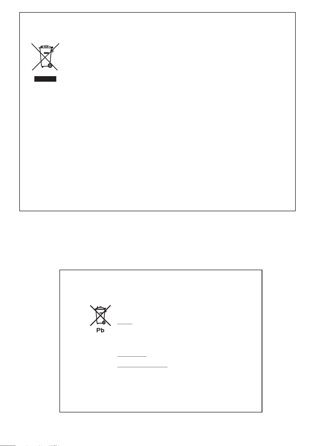
Information on Proper Disposal
A. Information on Disposal for Users (private households)
1. In the European Union
Attention: If you want to dispose of this equipment, please do not use the ordinary dust bin!
Used electrical and electronic equipment must be treated separately and in accordance with legislation that
requires proper treatment, recovery and recycling of used electrical and electronic equipment.
Following the implementation by member states, private households within the EU states may return their
used electrical and electronic equipment to designated collection facilities free of charge*. In some countries*
your local retailer may also take back your old product free of charge if you purchase a similar new one.
*) Please contact your local authority for further details.
If your used electrical or electronic equipment has batteries or accumulators, please dispose of these separately
beforehand according to local requirements.
Attention: Your product is
marked with this symbol.
It means that used
electrical and electronic
products should not be
mixed with general
household waste. There is
a separate collection
system for these
products.
By disposing of this product correctly you will help ensure that the waste undergoes the necessary treatment,
recovery and recycling and thus prevent potential negative effects on the environment and human health
which could otherwise arise due to inappropriate waste handling.
2. In other Countries outside the EU
If you wish to discard this product, please contact your local authorities and ask for the correct method of
disposal.
For Switzerland: Used electrical or electronic equipment can be returned free of charge to the dealer, even if
you don ’t purchas e a new prod uct. Furth er collect ion facili ties are listed on the homepag e of
www.swico.ch or www.sens.ch.
B. Information on Disposal for Business Users
1. In the European Union
If the product is used for business purposes and you want to discard it:
Please contact your SHARP dealer who will inform you about the take-back of the product. You might be
charged for the costs arising from take-back and recycling. Small products (and small amounts) might be
taken back by your local collection facilities.
For Spain: Please contact the established collection system or your local authority for take-back of your used
products.
2. In other Countries outside the EU
If you wish to discard of this product, please contact your local authorities and ask for the correct method of
disposal.
Information on Battery Disposal
The battery supplied with this product contains traces
of Lead.
For EU: The c rosse d-out w heele d bin i mp lies that
us e d batteri e s should no t b e p u t to t h e g e n e r a l
ho u s ehol d w a s te! Ther e is a s e par a t e c o lle c t i on
system for used batteries, to allow proper treatm ent
and recyc ling in accor dance with legis lation. Please
contact your local authority for details on the collection
and recycling schemes.
For Switzerland: The used battery is to be returned to
the selling point.
For other non-EU countries: Please contact your local
author ity for corre ct metho d of di sposal of the used
battery.
Page 3
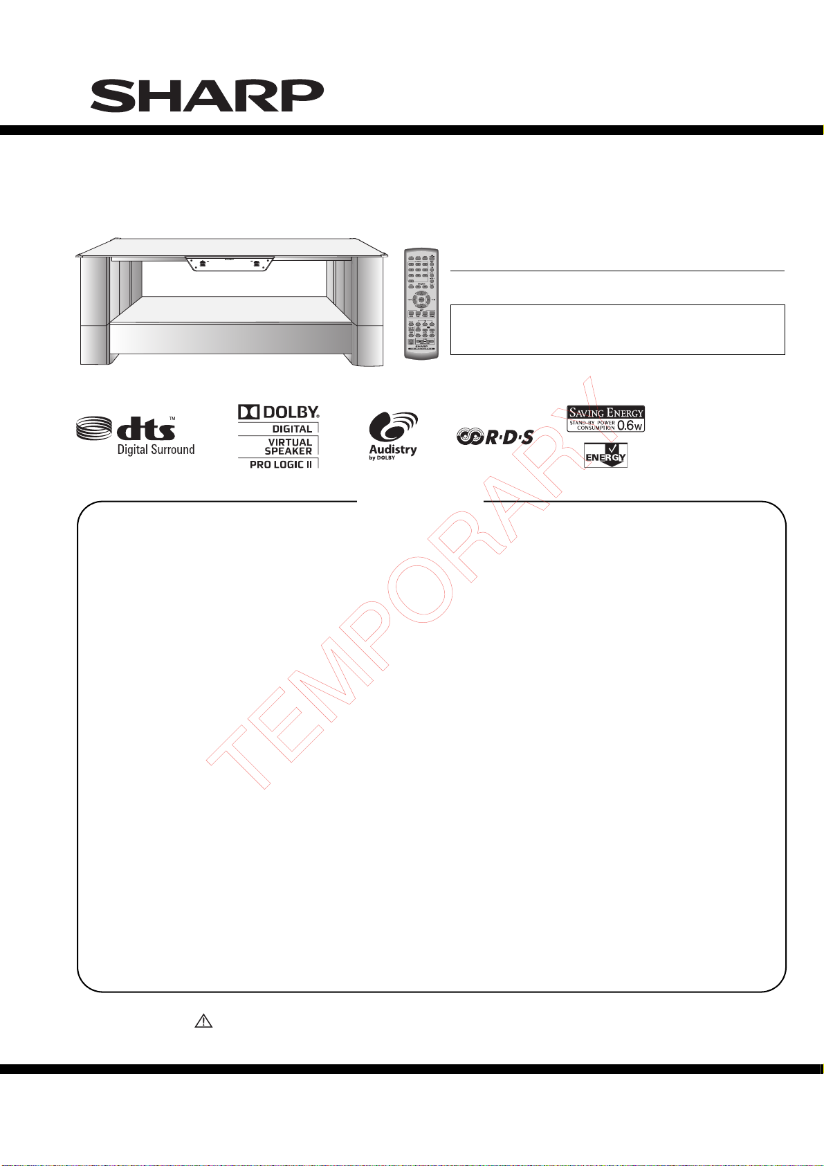
MODEL
AN-GR
500
H
HOME CINEMA RACK SYSTEM
This quick Start Guide will help you to correctly install and operate your system.
Accessories
1
If you require any advice or assistance regarding
your Sharp product, please visit our web-site
www.sharp.co.uk/customersupport.aspx
Customers without internet access may
telephone 0870 787 4837 during office hours (or
(01) 843 4711 if telephoning from Ireland).
Top glass x 1 Bottom glass x 1
Remote control x 1
Installing the glass and the glass protector
2
1. Fix the glass protector to the top glass at each corner.
Make sure the "TEMPERED" sticker on top of the glass
is facing up.
TOP VIEW
Step 1 Step 2
(UM/SUM-3, R6, HP-7 or similar)
"AA" size battery
x 2
2. Place the top glass on top of the frame.
Make sure all the glass protector guide is fitting to the frame hole.
“TEMPERED” sticker
FM aerial x 1
TEMPERED
Glass protector x 4
Adjustable nylon band x 3
Glass protector
TEMPERED
“TEMPERED” sticker
BOTTOM VIEW
Step 1
Notes:
It is advisable for the top glass to be carried by 2 persons.
Top glass with sticker on its surface, must face upwards.
Metal frame must not be removed to ensure safety.
The maximum load for the top glass on the unit is 100 kg.
The glasses are made of reinforced glass, but dropping pointed
objects on them or strongly hitting the surface may cause them to
break.
Top and bottom glass are not fastened to the unit. Always take
care when transporting it, otherwise these parts may fall off and
there is a risk of damage and injury.
TEMPERED
Step 2
Frame hole for
the glass protector
to fit in.
Subwoofer box
“TEMPERED”
sticker
Top glass
TEMPERED
Bottom
glass
3. Place the bottom glass on top of the subwoofer box.
Make sure the “TEMPERED” sticker on top of the glass is facing
up.
TINSEA270AWZZ
08G R MW 1
Page 4
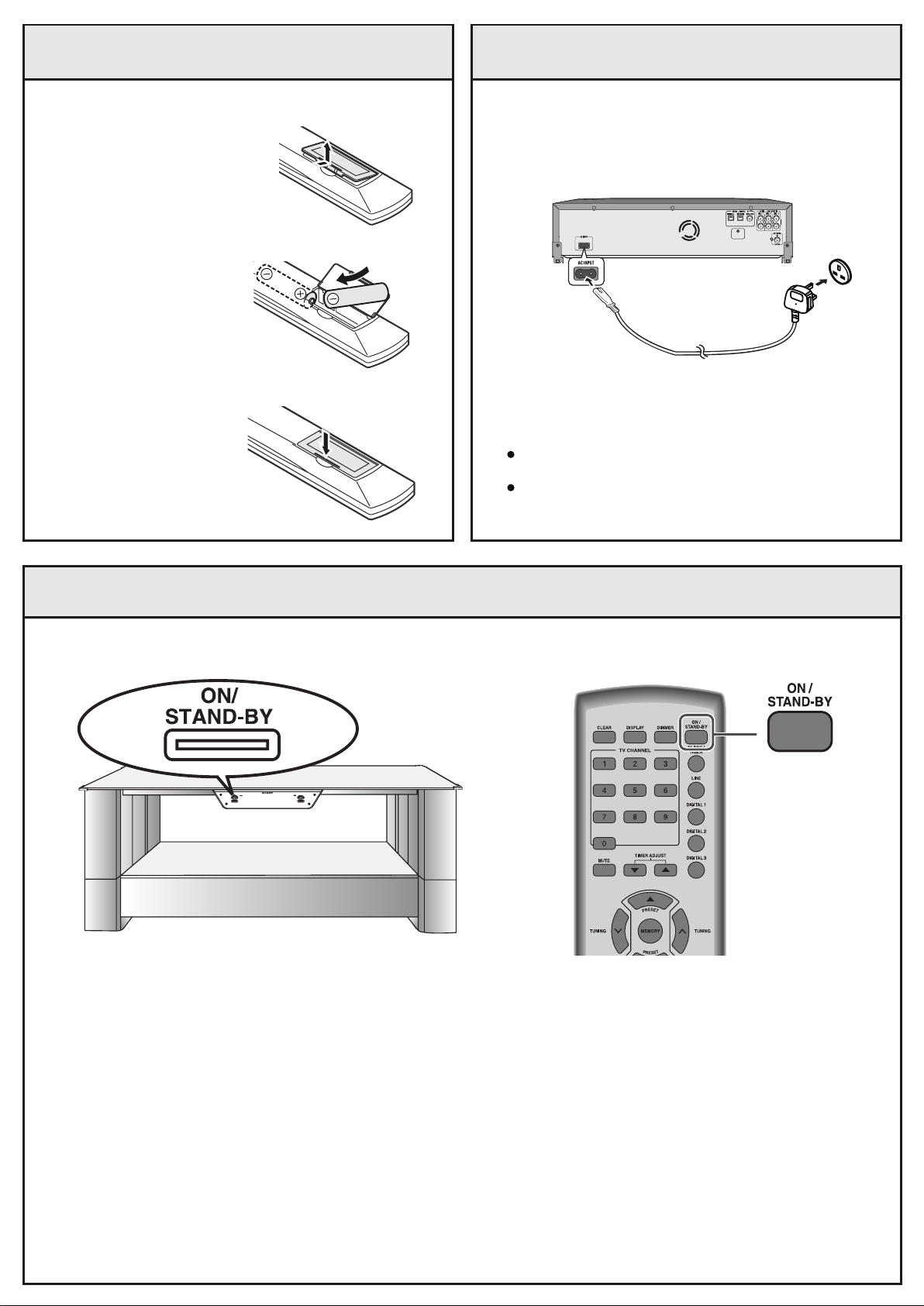
Remote control battery installation
3
Connecting the AC power lead
4
Use 2 “AA” size batteries (UM/SUM-3, R6, HP-7 or similar).
1 Open the battery cover.
2 Insert the batteries as shown.
3 Close the cover.
After checking all the connections have been made correctly,
connect the AC power lead to the AC power input socket, then to the
wall socket.
Wall socket
(AC 220 V- 240 V, 50 Hz)
Notes:
Never use a power lead other than the one supplied. Otherwise,
a malfunction or an accident may occur.
Unplug the AC power lead from the wall socket if the unit will not
be in use for a prolonged period of time.
To turn the power on
5
Press the ON/STAND-BY button.
If the power does not turn on, check whether the power lead is plugged in properly.
To set the unit to stand-by mode:
Press the ON/STAND-BY button again.
Note:
After the unit enters the power stand-by mode, wait a few seconds to turn on again
Page 5
AN-GR500H
SERVICE MANUAL
No. S7840ANR500HH
HOME CINEMA RACK SYSTEM
CONTENTS
PRECAUTIONS FOR USING LEAD FREE SOLDER
CHAPTER 1. GENERAL DESCRIPTION
[1] Specifications................................................ 1-1
[2] Names Of Parts ............................................ 1-2
CHAPTER 2. ADJUSTMENTS
[1] Description Of Error Messages..................... 2-1
[2] Test Mode ..................................................... 2-2
[3] EEPROM Mode ............................................ 2-2
[4] EEPROM List (Version: 02) .......................... 2-3
[5] KEY / LED Check Mode ............................... 2-5
[6] Quick Volume Change Mode ........................ 2-5
[7] Tuner Test Mode ........................................... 2-6
[8] ASPM Test Mode (For EU Destination) ........ 2-6
CHAPTER 3. MECHANISM BLOCKS
[1] Before Disassembly ...................................... 3-1
[2] Disassenbly Method ..................................... 3-2
CHAPTER 4. DIAGRAMS
[1] Main Block Diagrams.................................... 4-1
[2] Power Block Diagrams ................................. 4-9
[3] Display Block Diagrams ...............................4-11
[4] Amplifier Block Diagram.............................. 4-13
[5] Subwoofer Block Diagram .......................... 4-15
MODEL
AN-GR500H
[For Europe, U.K., Australia and New Zealand]
• In the interests of user-safety the set should be restored to its
original condition and only parts identical to those specified be
used.
CHAPTER 5. CIRCUIT DESCRIPTION
[1] To Check And Cancel Protect Circuit
Detection Line ............................................... 5-1
[2] Failure Detection Identification Using
STANDBY LED.............................................. 5-2
[3] Waveforms Of Subwoofer Circuit .................. 5-3
[4] Voltage .......................................................... 5-4
CHAPTER 6. CIRCUIT SCHEMATICS AND PARTS
LAYOUT
[1] Notes On Schematic Diagram....................... 6-1
[2] Types Of Transistor And LED........................ 6-1
[3] Schematic Diagram ....................................... 6-2
[4] Charts Of Connecting Wires........................ 6-18
[5] Wiring Side Of PWB.................................... 6-20
CHAPTER 7. OTHERS
[1] Function Table Of IC...................................... 7-1
[2] FL Display ................................................... 7-12
PARTS GUIDE
Parts marked with " " are important for maintaining the safety of the set. Be sure to replace these parts with specified
ones for maintaining the safety and performance of the set.
This document has been published to be used
SHARP CORPORATION
for after sales service only.
The contents are subject to change without notice.
Page 6
AN-GR500H
Audi
MP150S
lXLMP150Mark
E
oXL-
ervice Manua
et
PRECAUTIONS FOR USING LEAD-FREE SOLDER
1. Employing lead-free solder
2. Using lead-free wire solder
3. Soldering
"MAIN, POWER, DISPLAY, INTERFACE, AMPLIFIER, SUBWOOFER PWB" of this model employs lead-free solder.
The LF symbol indicates lead-free solder, and is attached on the PWB and service manuals. The alphabetical character
following LF shows the type of lead-free solder.
Example:
Indicates lead-free solder of tin, silver and copper.
When fixing the PWB soldered with the lead-free solder, apply lead-free wire solder. Repairing with conventional lead wire
solder may cause damage or accident due to cracks.
As the melting point of lead-free solder (Sn-Ag-Cu) is higher than the lead wire solder by 40 C, we recommend you to
dedicated soldering bit, if you are not familiar with how to obtain lead-free wire solder or soldering bit, contact our
use a
service station
As the melting point of lead-free solder (Sn-Ag-Cu) is about 220 C which is higher than the conventional lead solder
by 40 C,
extended period of
of parts may be exceeded,
Lead-free solder contains more tin, and the end of the soldering bit may be easily corrected. Make sure to turn on
and off the
If a different type of solder stays on the tip of the soldering bit, it is alloyed with lead-free solder. Clean the bit after
every use
When the tip of the soldering bit is blackened during use, file it with steel wool or fine sandpaper.
Be careful when replacing parts with polarity indication on the PWB silk.
Lead-free wire solder for servicing
Ref No.
PWB-A 92LPWB7358MANS MAIN
PWB-B 92LPWB7358PWRS POWER(B1), DISPLAY(B2), INTERFACE(B3)
PWB-C 92LPWB7358AMPS AMPLIFIER
PWB-D 92LPWB7358SWFS SUBWOOFER
or service branch in your area.
and as it has poor solder wettability, you may be apt to keep the soldering bit in contact with the PWB for
time. However, since the land may be peeled off or the maximum heat-resistance temperature
remove the bit from the PWB as soon as you confirm the steady soldering condition.
power of the bit as required.
of it.
Parts No.
Description
– i –
Page 7
AN-GR500H
CHAPTER 1: GENERAL DESCRIPTION
[1] Specifications
FOR A COMPLETE DESCRIPTION OF THE OPERATION OF THIS UNIT, PLEASE REFER TO THE
OPERATION MANUAL.
AN-GR500H AN-GR500H for U.K., Australia and New Zealand
• Main unit
Amplifier section
Power source AC 220 V - 240 V ~ 50 Hz
Power
consumption
Amplification
system
Frequency range FM: 87.5 - 108 MHz
Output power Front speaker:
Audio input
terminals
Front speaker section
Type 2-way type speaker system (Magnetic shield)
Impedance 6 ohms
General
Dimensions Width: 1105 mm (43-1/2")
Weight 38.25 kg (84.33 lbs.)
Glass on top of
unit
Power on: 63 W
Power stand-by: 0.6 W
Front speaker: Pulse width modulation
Subwoofer: Pulse width modulation
MPO: 100W (50W + 50W) (DIN 45 324)
RMS: 100W (50W + 50W) (DIN 45 324)
RMS: 90W (45W + 45W) (DIN 45 500)
Subwoofer:
MPO: 100W (DIN 45 324)
RMS: 100W (DIN 45 324)
RMS: 90W (DIN 45 500)
Optical digital input (DIGITAL 1/2): Square type x 2
Coaxial digital input (DIGITAL 3): RCA type x 1
Analog input (LINE 1): RCA type x 1 pair (L/R)
Analog input (LINE 2): RCA type x 1 pair (L/R)
Analog input (LINE 3): RCA type x 1 pair (L/R)
2.5 cm (1") Tweeter x 2
8 cm (3-1/8") Woofer x 2
Height: 482 mm (19")
Depth: 387 mm (15-1/4")
The maximum load/weight:100kg
• Main unit
Amplifier section
Power source AC 220 V - 240 V ~ 50 Hz
Power
consumption
Amplification
system
Frequency range FM : 87.5 - 108 MHz
Output power Front speaker:
Audio input
terminals
Front speaker section
Type 2-way type speaker system (Magnetic shield)
Impedance 6 ohms
General
Dimensions Width: 1105 mm (43-1/2")
Weight 38.25 kg (84.33 lbs.)
Glass on top of
unit
Power on: 63 W
Power stand-by: 0.6 W
Front speaker: Pulse with modulation
Subwoofer: Pulse with modulation
MPO: 100W (50W + 50W) (T.H.D. 10%)
RMS: 100W (50W + 50W) (T.H.D. 10%)
RMS: 90W (45W + 45W) (T.H.D. 0.9%)
Subwoofer:
MPO: 100W (T.H.D. 10%)
RMS: 100W (T.H.D. 10%)
RMS: 90W (T.H.D. 0.9%)
Optical digital input (DIGITAL 1/2): Square type x 2
Coaxial digital input (DIGITAL 3): RCA type x 1
Analog input (LINE 1): RCA type x 1 pair (L/R)
Analog input (LINE 2): RCA type x 1 pair (L/R)
Analog input (LINE 3): RCA type x 1 pair (L/R)
2.5 cm (1") Tweeter 2
8 cm (3 - 1/8") Woofer 2
Height: 482 mm (19")
Depth: 387 mm (15-1/4")
The maximum load/weight: 100 kg
•Subwoofer
Type Subwoofer system (Magnetic shield)
Maximum input
power
Impedance 12 ohms
• Remote control
Power source
Specifications for this model are subject to change without prior notice.
20 cm (8") Subwoofer
100 W
DC 3V ["AA" size (UM/SUM-3, R6, HP-7
or similar) battery x 2]
•Subwoofer
Type Subwoofer system (Magnetic shield)
20 cm (8") Subwoofer
Maximum input
power
Impedance 12 ohms
• Remote control
Power source DC 3V ["AA" size (UM/SUM-3, R6, HP-7 or
100 W
similar) battery 2]
1 – 1
Page 8
AN-GR500H
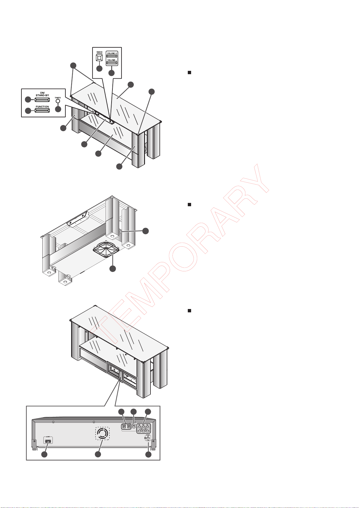
[2] Names Of Parts
11
1
2
3
4
8
9
10
11
5
6
7
Main Unit (front panel)
1. On/Stand-by Button
2. Function Button
3. Timer Indicator
4. Left Front Speakers
5. Display
6. Bottom glass
7. Right Front Speakers
8. Remote Sensor
9. Volume Up and Down Buttons
10. Top glass
11. Glass protector
Main unit (bottom panel)
1. Subwoofer
2. Bass Reflex Duct
2
1
Main unit (rear panel)
1. Optical Digital Audio Input Sockets
2. Coaxial Digital Audio Input Socket
3. Audio Line Input Sockets
4. AC Power Input Socket
5. Cooling Fan
6. FM 75 Ohms Aerial Socket
2
1
3
4
5
6
1 – 2
Page 9
AN-GR500H
9
87
1
2
3
4
5
6
1
2
3
16
17
18
4
19
20
21
5
6
7
22
23
24
8
25
9
10
11
12
13
26
27
28
29
30
14
15
31
10 11
13 14
12
16
15
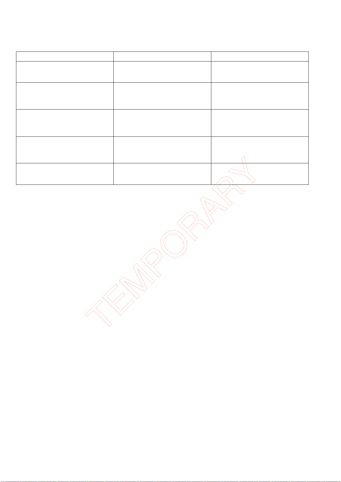
Remote control
1. Remote Control Transmitter
2. Display Button
3. Clear Button
4. TV Channel Number Button
5. Mute Button
6. Timer Adjust Up or Down Button
7. Preset Up Button
8. Tuning Down Button
9. Natural Bass Button
10. Sound Space Button
11. RDS ASPM Button
12. Tuner Button
13. Dolby Virtual Speaker Button
14. Sound Mode Button
15. Shift Button
16. Dimmer Button
17. ON/STAND-BY Button
18. Clock / Timer Button
19. Line Button
20. Digital 1 Button
21. Digital 2 Button
22. Digital 3 Button
23. Memory Button
24. Tuning Up Button
25. Preset Down Button
26. Intelligent Volume Button
27. Mono to Stereo Button
28. RDS PTY Button
29. RDS Display Button
30. TV Operation Buttons
31. Volume Up or Down Buttons
Display
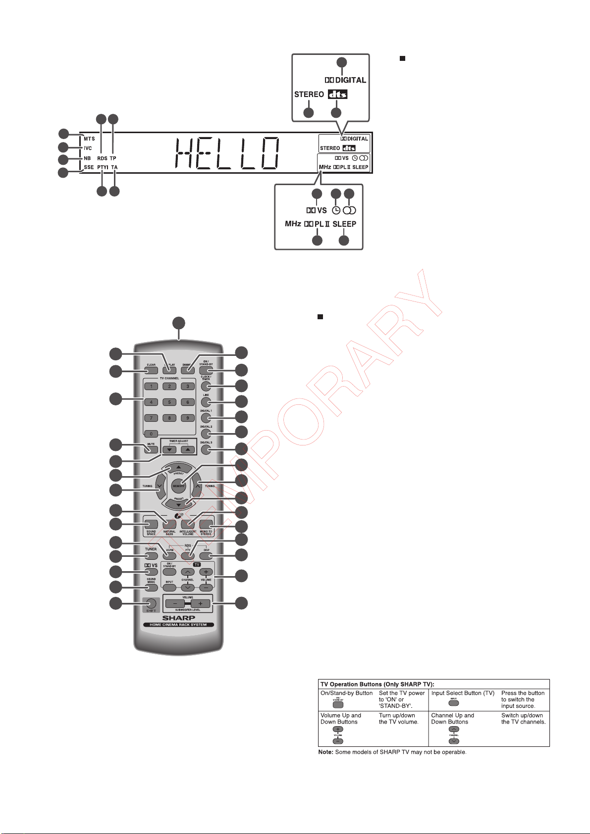
1. Mono to Stereo indicator
2. Intelligent Volume indicator
3. Natural Bass indicator
4. Sound Space indicator
5. Dynamic PTY indicator
6. Traffic Announcement indicator
7. RDS indicator
8. Traffic Programme indicator
9. Dolby Digital Signal indicator
10. FM Stereo Mode indicator
11. DTS Signal indicator
12. Dolby Virtual Sound indicator
13. Timer indicator
14. FM Stereo Receiving indicator
15. Dolby Prologic II indicator
16. Sleep indicator
1 – 3
Page 10
AN-GR500H
CD-ES700/CD-ES77CD-ES700/CD-ES77Service ManualCD-ES700/CD-ES77MarketE
CHAPTER 2. ADJUSTMENTS
[1] Description Of Error Messages
Error message Cause Solution
“ERR 01”
(Appears for 2 seconds and then the system
goes standby.)
“ERR 02”
(When this error is not detected, the initial
display appears.)
“ERR 03”
(When this error is not detected, the initial
display appears.)
“ERR 07”
(When this error is not detected, the initial
display appears.)
“ERR 80”
(When this error is not detected, the initial
display appears.)
* For other error messages using STANDBY LED, refer to the corresponding pages.
• Rotation stop of the fan motor • Check if the fan motor cord is inserted
• Error in the ICM6 (CS49510) control • Unplug the AC power cord and turn on
• Internal communication error of the system
[ICA1 (WM8775) or ICM3 (CS8416CN)]
• Internal communication error of the system
[ICM10 (LC750512)]
• Internal data read access error of ICM8
(CAT24WC05YI)
properly and the fan motor is not locked.
power again.
• Check the line connected between ICM6
and ICM7.
• Unplug the AC power cord and turn on
power again.
• Check the line connected among ICA1,
ICM3, ICM8 and ICM7.
• Unplug the AC power cord and turn on
power again.
• Check the line connected between ICM10
and ICM7.
• Check EEPROM data.
• Replace EEPROM IC (ICM8).
2 – 1
Page 11
[2] Test Mode
AN-GR500H
1. Entering the test mode
In the AC OFF state, hold down the “FUNCTION” key and press the
POWER key. Then switch on AC to enter the test mode route state.
* Be sure to follow the above procedure to enter the test mode.
2. Exiting the test mode
In the test mode route state, press the POWER key to turn off the
system and exit the test mode.
3. Operation
(Test mode start-up operation)
↓
GR8529BH
(POWER key)
↓
GOOD BYE
Version Display
(example version date is
29/05/2008)
Display “GOOD BYE”
(as in the case of the user
mode)
[3] EEPROM Mode
When replacing EEPROM IC, necessary data are not recorded
inside; “Protect area read error” (“ERR 80”) occurs.
To avoid this state, write the data into the corresponding device.
1. Enter the test mode and check set data values of each address
according to the EEPROM set data table on the right.
If necessary, change the set data values.
NOTE: (Data are written into EEPROM in the procedure 4 below.)
(Do not stop power supply to the product)
4. Remote control key operation
Key operation is described by using the names of the main unit keys.
For remote control key operation, each test can be enter directly as
follow.
* However, remote control keys are unavailable for starting the test
mode.
Remote Control Key Test Mode
MUTE key Volume Test
DVS key Key Test
SOUND MODE key EEPROM Mode Test
TUNER key Tuner Test
ASPM key ASPM Test
* Remote control keys are unavailable for starting the test mode.
GR8529BH
Test mode route state
(Example Micom version date 29/5/2008)
↓
EEP TEST
Mode menu “EEPROM“
(VOLUME + key): EEPROM mode start-up
↓
EEPROM address display (25Ah)
(VOLUME + key): Address increment
EEPROM address display (25Bh)
(VOLUME key) ↑ ↓
EEP 025A
↑ ↓
EEP 025B
↑ ↓
EEP 025C
EEP 03FE
↑ ↓
EEP 03FF
2. Exiting the EEPROM mode from the address value display state.
(Press the POWER key once in the address value display state.)
(The product enters the test mode route state.)
3. Exiting the test mode
(Press the POWER key once in the test mode route state.)
(Then the data are written into EEPROM. After the write
operation, the product enters the standby state.)
EEPROM address display (3FF h)
(Input select key)
←
→
At each address
(Input select key) (Set value change by
4. After checking that the product enters the standby state, stop
power supply to the product.
(This operation initializes the error state.)
* Operation ends.
EEP 005A
↑ ↓
VOLUME +/– keys)
Set data value display
(2 Hz flasing)
2 – 2
Page 12
AN-GR500H
㧗㧜㧜㧴
㧗㧜㧝㧴
㧗㧜㧜㧴
㧗㧜㧝㧴
㧗㧜㧜㧴
㧗㧜㧜㧴
㧗㧜㧝㧴
㧗㧜㧝㧴
[4] EEPROM List (Version: 02) (1/2)
ADDRESS 㧗㧜㧜㧴
㧗㧜㧝㧴
ADDRESS
㧗㧜㧜㧴
㧗㧜㧝㧴
HEX ITEM CODE ITEM CODE HEX ITEM CODE ITEM CODE
025A 602 PVER 02h AUMD
#REF! 07h 02B2 690 GPDO3 B6h 48 9Dh
025C 604 ITVL 25h ITVC 01h 02B4 692 GPDFH 05h 50 0Ch
025E 606 NBCF 05h NBLV 65h 02B6 694 GPDF3 33h 52 5Dh
0260 608 INISW FFh
CHECK-SUM 67h 02B8 696 GADOH 14h 54 18h
0262 610 reserved FFh reserved FFh 02BA 698 GADO3 57h 56 E9h
0264 612 reserved FFh reserved FFh 02BC 700 GADFH 0Fh 58 F6h
0266 614
CHECK-SUM 03h OFGA 00h 02BE 702 GADF3 4Ch 60 16h
0268 616 OFBS 00h OFTR 00h 02C0 704 GDDOH 08h 62 00h
026A 618 reserved FFh CIGA 02h 02C2 706 GDDO3 00h 64 00h
026C 620 CIBS 00h CITR 03h 02C4 708 GDDFH 0Bh 66 4Ch
026E 622 reserved FFh ANGA 00h 02C6 710 GDDF3 E0h 68 7Bh
0270 624 ANBS 0Bh ANTR 05h 02C8 712 GCDOH 09h 70 82h
0272 626 reserved FFh SOGA 02h 02CA 714 GCDO3 0Dh 72 74h
0274 628 SOBS 00h SOTR 03h 02CC 716 GCDFH 0Bh 74 4Ch
0276 630 reserved FFh SPGA 02h 02CE 718 GCDF3 E0h 80 7Bh
0278 632 SPBS 00h SPTR 03h 02D0 720 GaDOH 14h 82 18h
027A 634 reserved FFh LAGA 02h 02D2 722 GaDO3 57h 84 E9h
027C 636 LABS 00h LATR 03h 02D4 724 GaDFH 07h 86 21h
027E 638 reserved FFh reserved FFh 02D6 726 GaDF3 48h 88 2Bh
0280 640
CHECK-SUM E2h E48AU 3Ch 02D8 728 reserved 2Bh 90 9Ah
0282 642 E48AM 39h E48AL 83h 02DA 730 0 FFh 92 FF
0284 644 E48BU A0h E48BM A3h 02DC 732 2 9Ah 94 FF
0286 646 E48BL 60h E48CU 29h 02DE 734 4 FFh 96 FF
0288 648 E48CM EBh E48CL F2h 02E0 736 6FF98FF
028A 650 E48DU 5Fh E48DM 5Ch 02E2 738 8 FF 100 FF
028C 652 E48DL 9Fh E48EU D9h 02E4 740 10 FF 102 FF
028E 654 E48EM DAh E48EL 8Ah 02E6 742 12 FF 104 FF
0290 656 E44AU 3Bh E44AM F9h 02E8 744 14 FF 106 FF
0292 658 E44AL E1h E44BU A3h 02EA 746 16 FFh 108 FFh
0294 660 E44BM 71h E44BL 6Dh 02EC 748 18 FFh 110 FFh
0296 662 E44CU 28h E44CM 77h 02EE 750 20 FFh 112 FFh
0298 664 E44CL D4h E44DU 5Ch 02F0 752 22 FFh 114 FFh
029A 666 E44DM 8Eh E44DL 93h 02F2 754 24 FFh 116 FFh
029C 668 E44EU DBh E44EM 8Eh 02F4 756 26 FFh 118 FFh
029E 670 E44EL 49h E32AU 3Ah 02F6 758 28 FFh 120 FFh
02A0 672 E32AM F6h E32AL 2Eh 02F8 760 30 FFh 122 FFh
02A2 674 E32BU B0h E32BM 47h 02FA 762 32 FFh 124 FFh
02A4 676 E32BL CFh E32CU 22h 02FC 764 34 FFh 126 FFh
02A6 678 E32CM 89h E32CL 1Bh 02FE 766 36 FFh 128 FFh
02A8 680 E32DU 4Fh E32DM B8h 0300 768 38 FFh 130 FFh
02AA 682 E32DL 30h E32EU E2h 0302 770 40 FFh 132 FFh
02AC 684 E32EM 80h E32EL E6h 0304 772 42 FFh 134 FFh
02AE 686 reserved FFh
CHECK-SUM 27h 0306 774 44 FFh 136 FFh
02B0 688 GPDOU 0Fh GPDO2 11h 0308 776 46 FFh 138 FFh
ADDRESS 㧗㧜㧜㧴
㧗㧜㧝㧴
ADDRESS
㧗㧜㧜㧴
㧗㧜㧝㧴
HEX ITEM CODE ITEM CODE HEX ITEM CODE ITEM CODE
030A 778 RM32
030C 780 RM34
030E 782 RM36
0310 784 RM38
0312 786 RM40
0314 788 RM42
0316 790 RM44
0318 792 RM46
031A 794 RM48
031C 796 RM50
031E 798 RM52
0320 800 RM54
0322 802 RM56
0324 804 RM58
0326 806 RM60
0328 808 RM62
032A 810 RM64
032C 812 RM66
032E 814 RM68
0330 816 RM70
FFh
FFh
FFh
FFh
FFh
FFh
FFh
FFh
FFh
FFh
FFh
FFh
FFh
FFh
FFh
FFh
FFh
FFh
FFh
FFh
RM33
RM35
RM37
RM39
RM41
RM43
RM45
RM47
RM49
RM51
RM53
RM55
RM57
RM59
RM61
RM63
RM65
RM67
RM69
RM71
FFh
FFh
FFh
FFh
FFh
FFh
FFh
FFh
FFh
FFh
FFh
FFh
FFh
FFh
FFh
FFh
FFh
FFh
FFh
FFh
0332 818 RM72
0334 820 RM74
0336 822 RM76
0338 824 RM78
033A 826 RM80
033C 828 RM82
033E 830 RM84
0340 832 RM86
0342 834 RM88
836 RM90
0344
0346 838 RM92
0348 840 RM94
034A 842 RM96
034C 844 RM98
034E 846 RM100
0350 848 RM102
0352 850 RM104
0354 852 RM106
0356 854 RM108
856 RM110
0358
FFh
FFh
FFh
FFh
FFh
FFh
FFh
FFh
FFh
FFh
FFh
FFh
FFh
FFh
FFh
FFh
FFh
FFh
FFh
FFh
RM73
RM75
RM77
RM79
RM81
RM83
RM85
RM87
RM89
RM91
RM93
RM95
RM97
RM99
RM101
RM103
RM105
RM107
RM109
CHECK-SUM
FFh
FFh
FFh
FFh
FFh
FFh
FFh
FFh
FFh
FFh
FFh
FFh
FFh
FFh
FFh
FFh
FFh
FFh
FFh
EFh
2 – 3
Page 13
[4] EEPROM List (Version: 02) (2/2)
A
A
A
A
A
4
6
A
A
A
A
A
A
㧗㧜㧝㧴
㧗㧜㧜㧴
㧗㧜㧝㧴
㧗㧜㧜㧴
㧗㧜㧝㧴
㧗㧜㧜㧴
㧗㧜㧝㧴
㧗㧜㧜㧴
㧗㧜㧝㧴
㧗㧜㧜㧴
AN-GR500H
ADDRESS 㧗㧜㧜㧴
HEX ITEM CODE ITEM CODE HEX ITEM CODE ITEM CODE
035
035C 860 RM58
035E 862 RM60
036
036C 876 RM74
036E 878 RM76
037
037C 892 RM90
037E 894 RM92
03A
03AC 940 RM82
03AE 942 RM84
03B0 944 RM86
03B2 946 RM88
03B4 948 RM90
03B6 950 RM92
03B8 952 RM94
03B
03BC 956 RM98
03BE 958 RM100
03C0 960 RM102
03C2 962 RM104
03C4 964 RM106
03C6 966 RM108
03C8 968 RM110
03C
03CC 972 RM114
03CE 974 RM116
03D0 976 RM118
858 RM56
0360 864 RM62
0362 866 RM64
0364 868 RM66
0366 870 RM68
0368 872 RM70
874 RM72
0370 880 RM78
0372 882 RM80
0374 884 RM82
0376 886 RM84
0378 888 RM86
890 RM88
0380 896 RM94
ADDRESS 㧗㧜㧜㧴
HEX ITEM CODE ITEM CODE HEX ITEM CODE ITEM CODE
938 RM80
954 RM96
970 RM112
FFh
FFh
FFh
FFh
FFh
FFh
FFh
FFh
FFh
FFh
FFh
FFh
FFh
FFh
FFh
FFh
FFh
FFh
FFh
FFh
FFh
FFh
FFh
FFh
FFh
FFh
FFh
FFh
FFh
FFh
FFh
FFh
FFh
FFh
FFh
FFh
FFh
FFh
FFh
FFh
RM57
RM59
RM61
RM63
RM65
RM67
RM69
RM71
RM73
RM75
RM77
RM79
RM81
RM83
RM85
RM87
RM89
RM91
RM93
RM95
RM81
RM83
RM85
RM87
RM89
RM91
RM93
RM95
RM97
RM99
RM101
RM103
RM105
RM107
RM109
RM 111
RM113
RM115
RM117
RM119
㧗㧜㧝㧴
㧗㧜㧝㧴
FFh
FFh
FFh
FFh
FFh
FFh
FFh
FFh
FFh
FFh
FFh
FFh
FFh
FFh
FFh
FFh
FFh
FFh
FFh
FFh
FFh
FFh
FFh
FFh
FFh
FFh
FFh
FFh
FFh
FFh
FFh
FFh
FFh
FFh
FFh
FFh
FFh
FFh
FFh
FFh
ADDRESS
0382 898 RM96
0384 900 RM98
0386 902 RM100
0388 904 RM102
906 RM104
038
038C 908 RM106
038E 910 RM108
0390 912 RM110
0392 914 RM112
0394 916 RM114
0396 918 RM116
0398 920 RM118
922 RM120
039
039C 924 RM122
039E 926 RM124
03A0 928 RM126
03A2 930 RM128
03A
932 RM130
03A
934 RM132
03A8 936 RM134
ADDRESS 㧗㧜㧜㧴
03D2 978 RM120
03D4 980 RM122
03D6 982 RM124
03D8 984 RM126
986 RM128
03D
03DC 988 RM130
03DE 990 RM132
03E0 992 RM134
03E2 994 RM136
03E4 996 RM138
03E6 998 RM140
03E8 1000 RM142
03E
1002 RM144
03EC 1004 RM146
03EE 1006 RM148
03F0 1008 RM150
03F2 1010 RM152
03F4 1012 RM154
03F6 1014 RM156
03F8 1016 RM158
㧗㧜㧜㧴
FFh
FFh
FFh
FFh
FFh
FFh
FFh
FFh
FFh
FFh
FFh
FFh
FFh
FFh
FFh
FFh
FFh
FFh
FFh
FFh
FFh
FFh
FFh
FFh
FFh
FFh
FFh
FFh
FFh
FFh
FFh
FFh
FFh
FFh
FFh
FFh
FFh
FFh
FFh
FFh
RM97
RM99
RM101
RM103
RM105
RM107
RM109
RM 111
RM113
RM115
RM117
RM119
RM121
RM123
RM125
RM127
RM129
RM131
RM133
0
RM121
RM123
RM125
RM127
RM129
RM131
RM133
RM135
RM137
RM139
RM141
RM143
RM145
RM147
RM149
RM151
RM153
RM155
RM157
0
㧗㧜㧝㧴
FFh
FFh
FFh
FFh
FFh
FFh
FFh
FFh
FFh
FFh
FFh
FFh
FFh
FFh
FFh
FFh
FFh
FFh
FFh
0
㧗㧜㧝㧴
FFh
FFh
FFh
FFh
FFh
FFh
FFh
FFh
FFh
FFh
FFh
FFh
FFh
FFh
FFh
FFh
FFh
FFh
FFh
0
ADDRESS 㧗㧜㧜㧴
HEX ITEM CODE ITEM CODE
03F
1018 RM104
03FC 1020 RM106
03FE 1022 RM108
FFh
FFh
FFh
RM105
RM107
RM109
㧗㧜㧝㧴
FFh
FFh
FFh
NOTES:
(1) Use an attached HEX format file for setup of data to EEPROM writer.
(2) EEPROM currently used for this model is made in CATALYST. It is CAT24WC05YI.
2 – 4
Page 14
AN-GR500H
[5] KEY / LED Check Mode
Display of 7-segment LED and each single LED
Transition during start-up
GR8529BH
Test mode route state
(Input select key)
↓
KEY TEST
Using FUNCTION key select “KEY TEST”
Press Volume (–) / (+) key to enter KEY TEST
Press key according to below check key
response or LED light-up table
↓
**
Press POWER key to return to Test Mode route state.
[6] Quick Volume Change Mode
Purpose
The purpose of this mode is inspection time shortening in the
production.
This mode is the same as the USER MODE except for the volume
operation.
Volume operation in this mode becomes a change in a step only to
the necessary position in inspection process.
KEY FL DISPLAY
FUNCTION + VOLUME (–) FL all light-up
LED light-up
FUNCTION KEY 1-1
VOLUME + KEY 1-2
VOLUME – KEY 1-3
The specification of operation
Main volume operation at QUICK VOL CHANGE MODE
Only the following position of volume can be set up in this mode.
VOLUME 0
(VOL+)(VOL–)
↑ ↓
VOLUME 1
(VOL+)(VOL–)
↑ ↓
VOLUME 10
(VOL+)(VOL–)
↑ ↓
VOLUME 20
(default value at QUICK VOL CHANGE MODE start)
(VOL+)(VOL–)
↑ ↓
VOLUME 30
(VOL+)(VOL–)
↑ ↓
VOLUME 40
NOTES:
(1) About operation specification of "VOL +/– key".
(2) A difference from this mode and the user mode is only a possible
volume steps and initial value after the mode start.
2 – 5
Page 15
[7] Tuner Test Mode
Outline
This Test Mode control are same with Normal Power-ON, only
Power-ON in TUNER function.
After Power-ON the operation and display are same but the TUNER
preset already memory as table below.
TEST Mode Operation
Set will Power-ON same process like user Power-ON, but direct to
TUNER Function Preset No. 1 of table below.
Set Preset Memory will be set as below table.
AN-GR500H
Destination
P1 87.50M
Preset Memory No.
SPAN
Key operation after Power ON are same with User Power-ON.
* When Test Mode end, Tuner Preset Memory will be initialize.
Others Memory initialize is not neccesry.
EU㧔H㧕
108.00MP2
90.00MP3
106.00MP4
98.00MP5
50K/9K
[8] ASPM Test Mode (For EU Destination)
Outline
At Tuner RDS ASPM operation need to be confirm for EU(H) model
only.
Power-ON in TUNER function, and scanning frequency from
105.00MHz - 108.00MHz.
And RDS station Preset Memory maximum 3 station.
TEST Mode Operation
Power ON in TUNER Function 106.50MHz FM Stereo Band. At
same time Only Preset No. ch1 - ch3 leave blank and all ch4 - ch40
memory at 87.50MHz FM Stereo Band.
With the press of ASPM key, ASPM operation will start at
105.00MHz frequency.
If RDS station received Preset will memory from ch1. (There is no
need to memory PS name in ASPM Test Mode. If preset change
during Test Mode Frequency will be display first)
Scan will stop after reach frequency 108.00MHz, and return to
frequency 106.50MHz FM Stereo.
To confirm Memory content display will show Preset Number and
frequency for ch1until ch3. After display are confirmed frequency will
return to 106.50MHz FM STEREO. (Display method same with
Tuner display during Normal POWER ON.)
If ASPM key is press again, ASPM operation will start from 2 untill
5.
While scanning if 3 station memorized, Scanning will stop and
operation 4 and 5 will take place.
Afterward, even if ASPM key input detect ASPM operation will not be
execute. "__END__" displayed and operation canceled.
Additional
Other then above, operation for ASPM are same with User
operation. So, when 1st time scan with same PI code Station with
most strong signal will be memory and will not be memory many
time. For 2nd and more station with same frequency will not be
memory.
But, if different station with same PI code (same PI with different
frequency station), station one with most strong signal will be
memory.
So, station that already memorized before scan will be ignore.
Therefore, even station with same same PI code after 3 times ASPM
scan, It is possible that, 3 station will be memorized in Signal Strong
order.
After Test Mode end only Tuner preset memory will be reset and set
to default. Ohers Memory, no need to be initialize.
2 – 6
Page 16
AN-GR500H
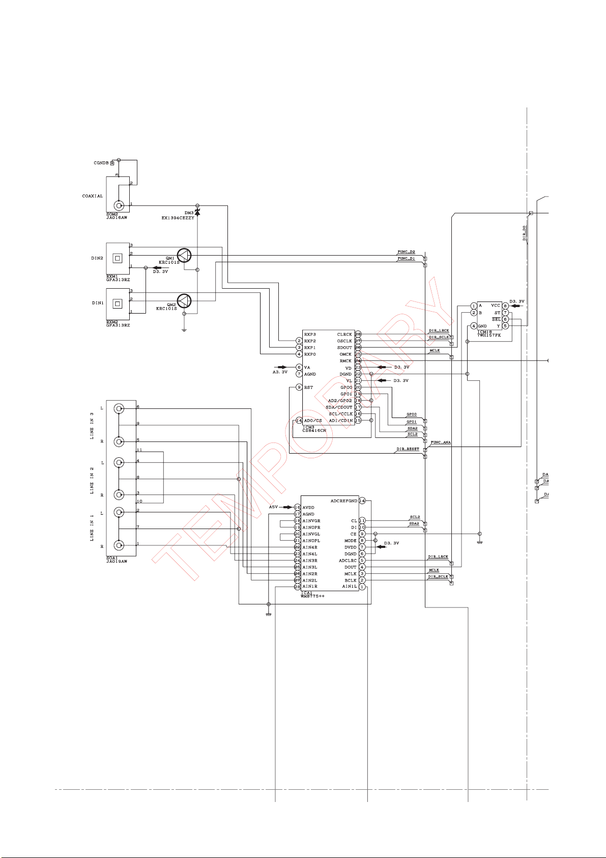
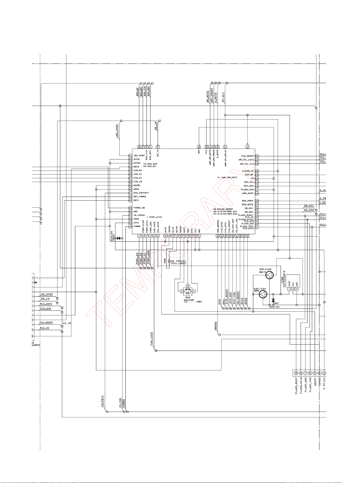
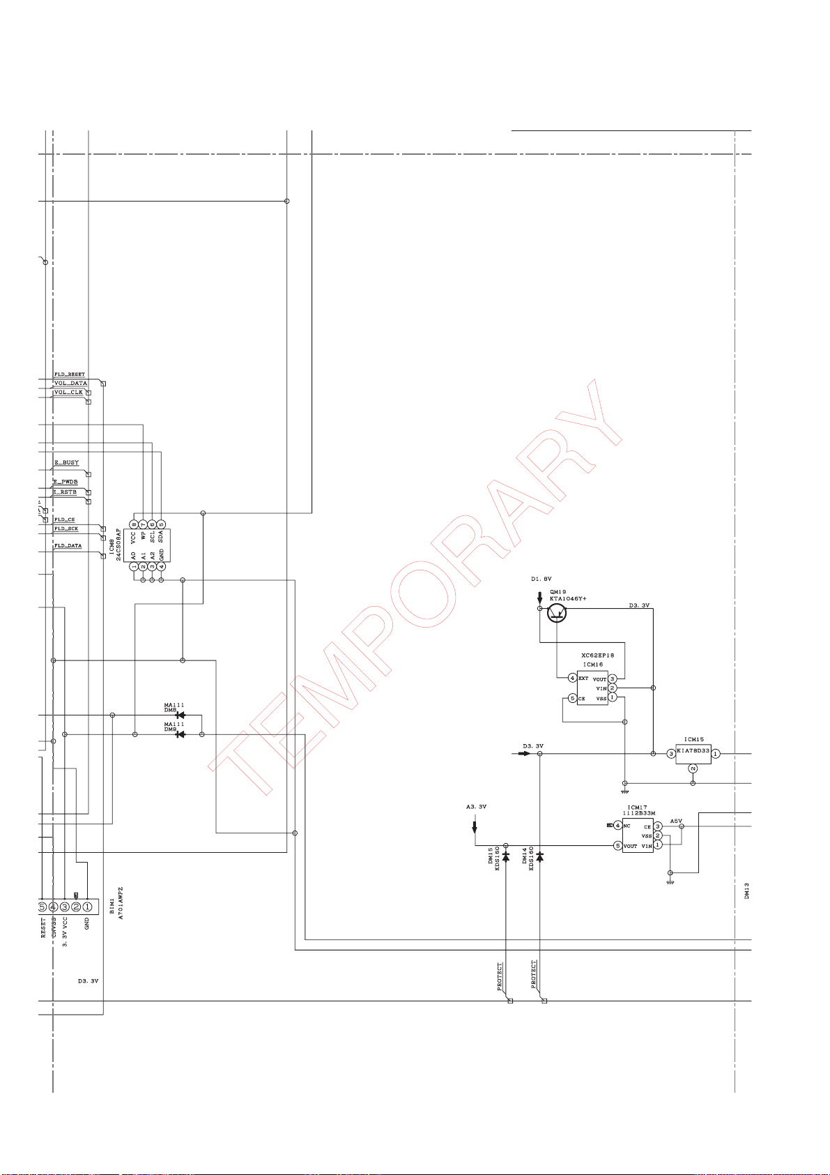
CHAPTER 4. DIAGRAMS
[1] Main Block Diagrams
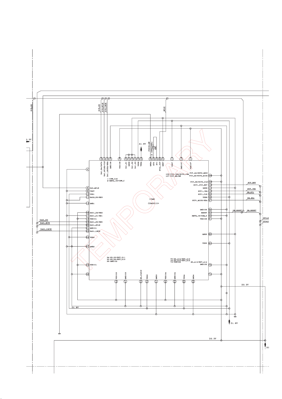
Figure 4-1: BLOCK DIAGRAM (1/8)
4 – 1
Page 17
AN-GR500H
Figure 4-2: BLOCK DIAGRAM (2/8)
4 – 2
Page 18
AN-GR500H
Figure 4-3: BLOCK DIAGRAM (3/8)
4 – 3
Page 19
AN-GR500H
Figure 4-4: BLOCK DIAGRAM (4/8)
4 – 4
Page 20
AN-GR500H
Figure 4-5: BLOCK DIAGRAM (5/8)
4 – 5
Page 21
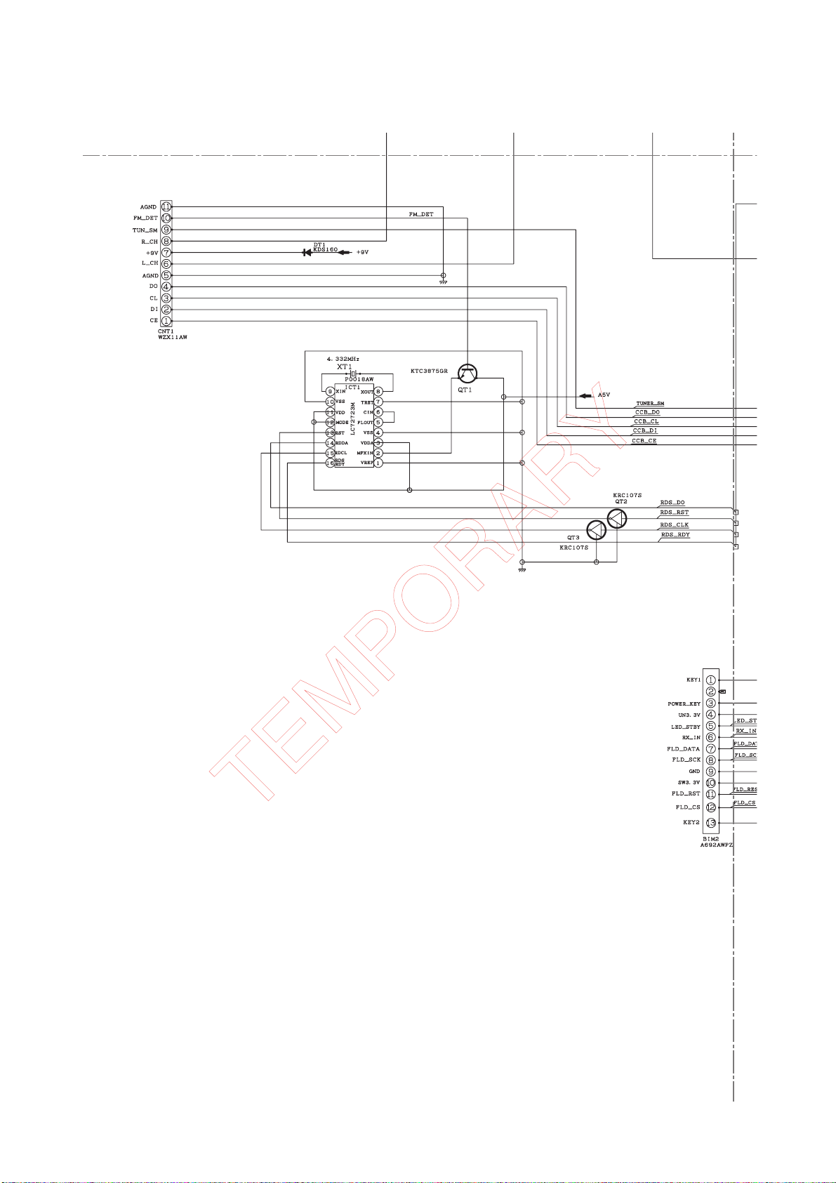
ICM7
IXA225AW
M3030RFGPFP
AN-GR500H
Figure 4-6: BLOCK DIAGRAM (6/8)
4 – 6
Page 22
AN-GR500H
Figure 4-7: BLOCK DIAGRAM (7/8)
4 – 7
Page 23
AN-GR500H
Figure 4-8: BLOCK DIAGRAM (8/8)
4 – 8
Page 24
AN-GR500H
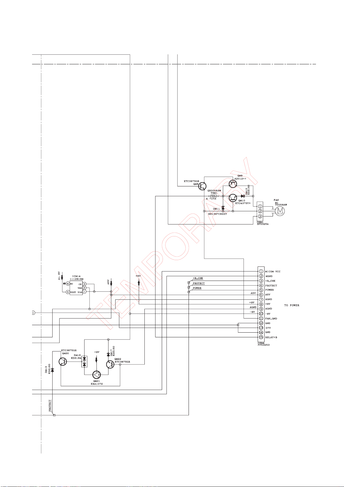
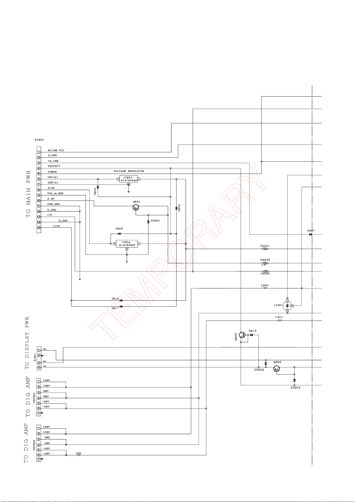
[2] Power Block Diagrams
Figure 4-9: POWER BLOCK DIAGRAM (1/2)
4 – 9
Page 25
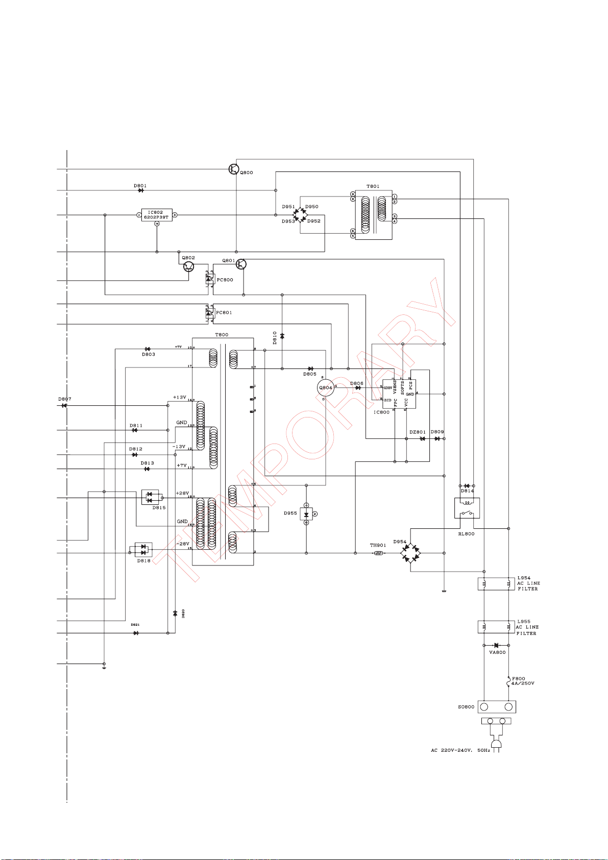
AN-GR500H
Figure 4-10: POWER BLOCK DIAGRAM (2/2)
4 – 10
AC POWER SUPPLY
Page 26
AN-GR500H
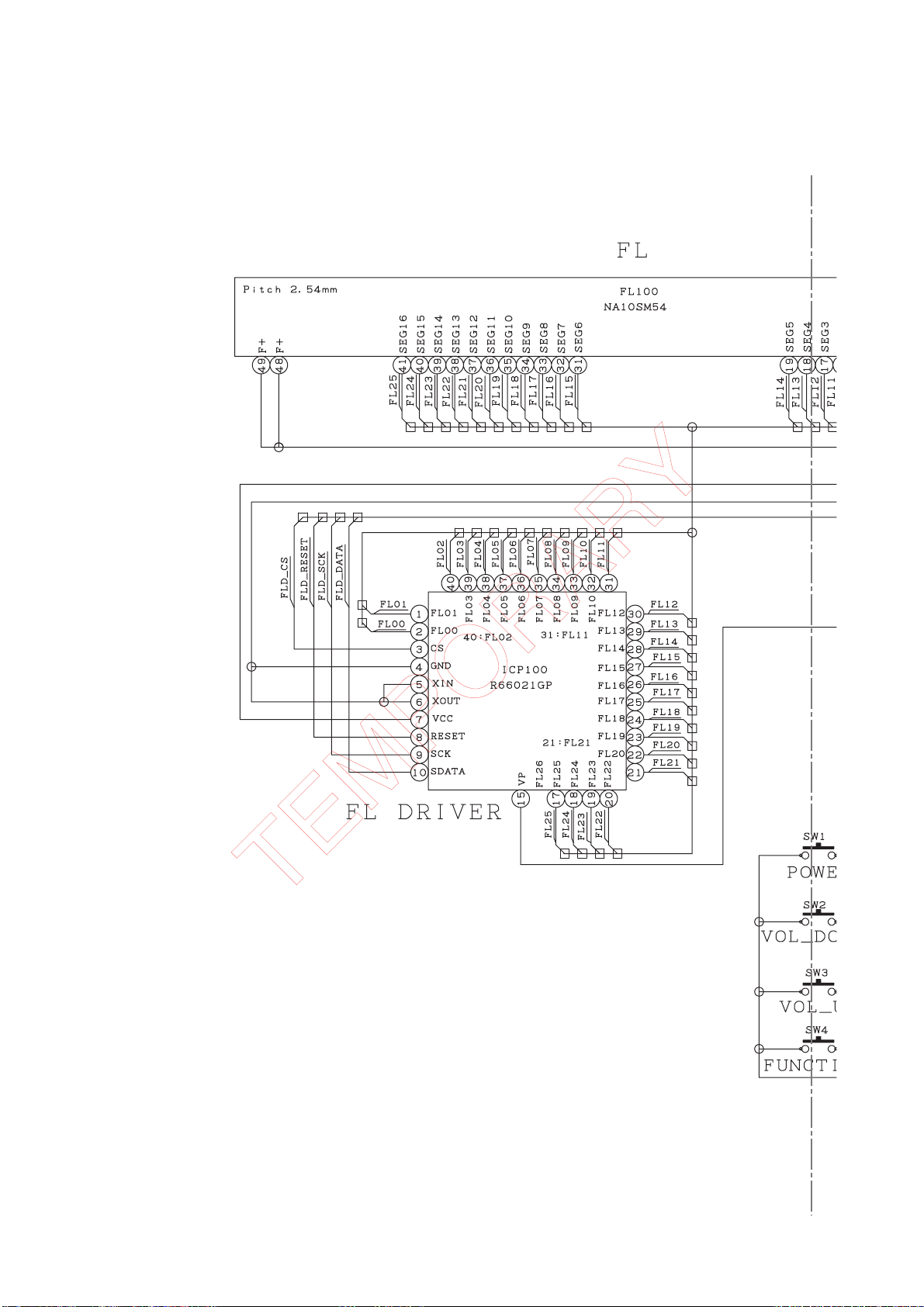
[3] Display Block Diagrams
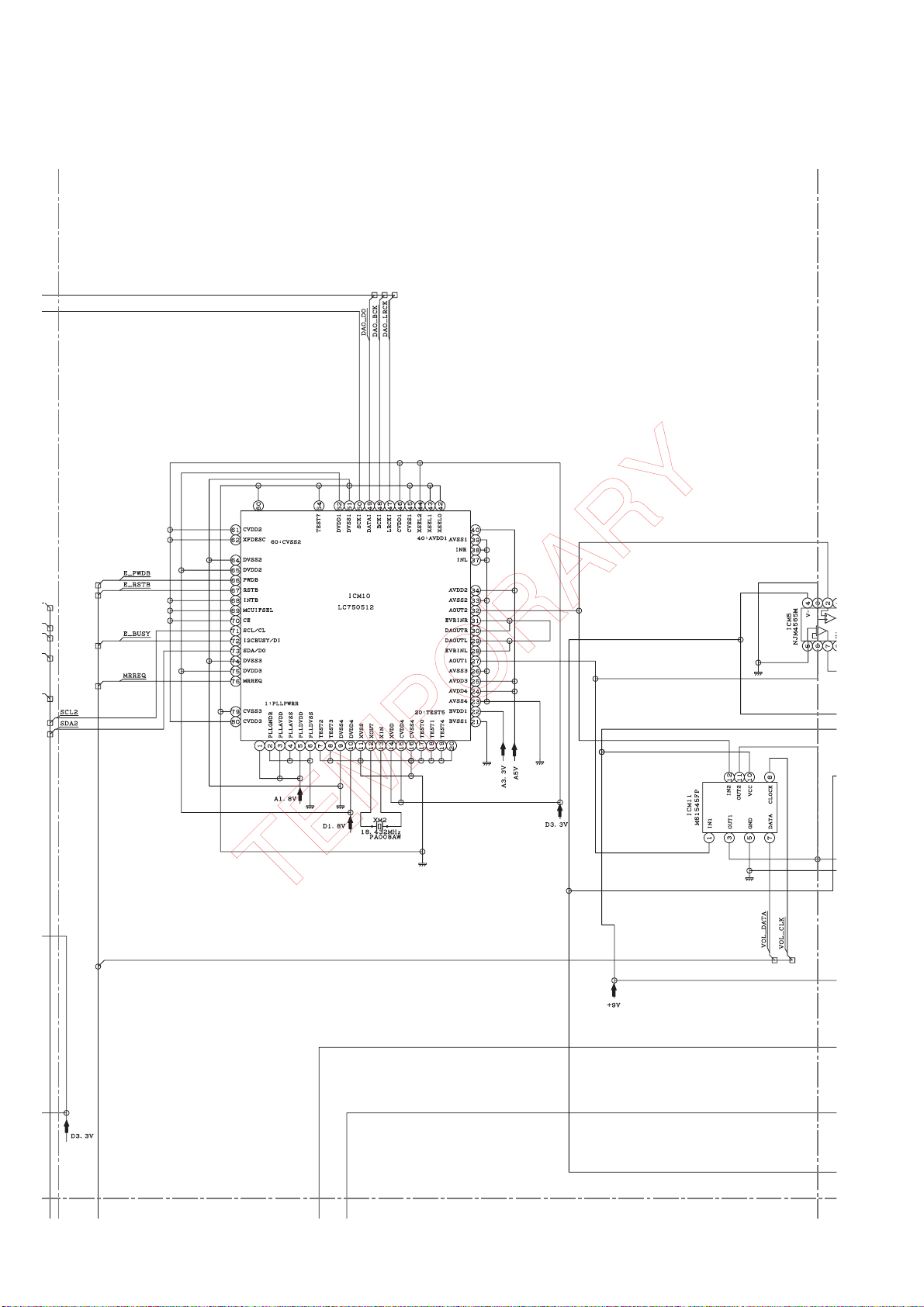
Figure 4-11: DISPLAY BLOCK DIAGRAM (1/2)
4 – 11
Page 27
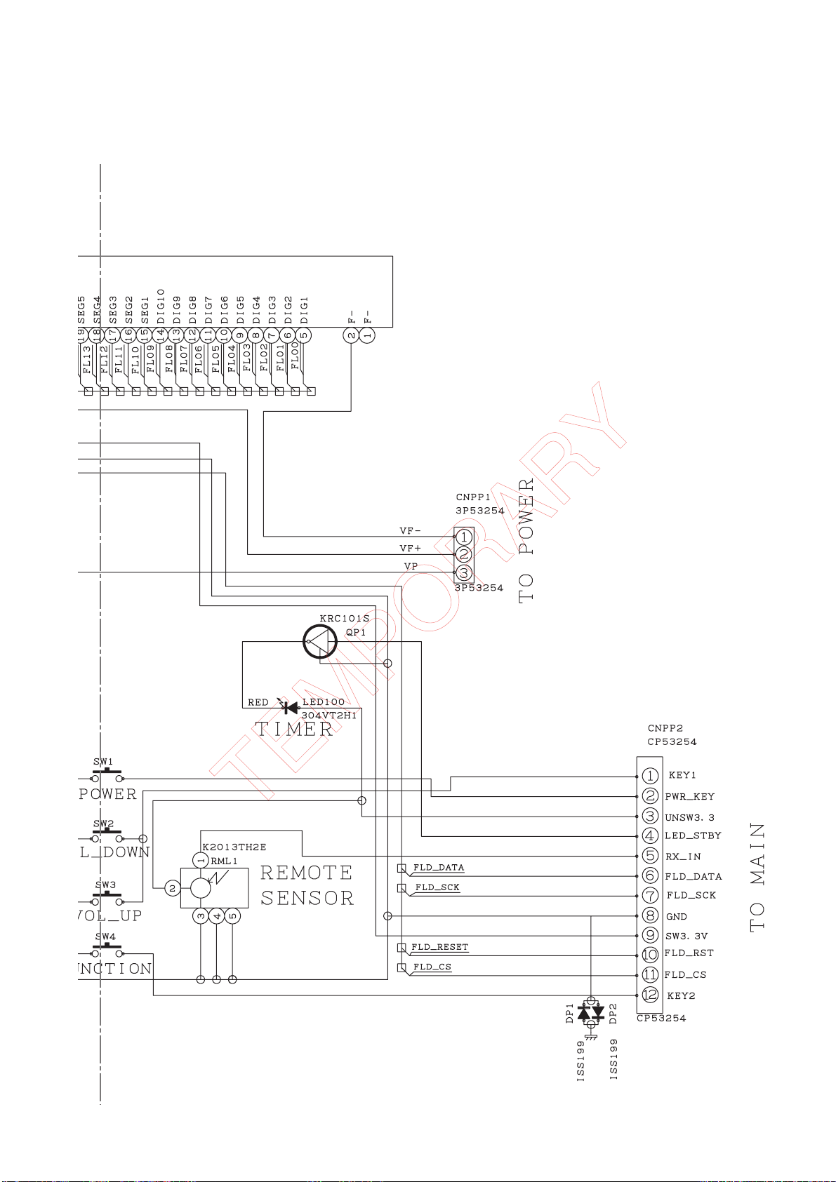
AN-GR500H
Figure 4-12: DISPLAY BLOCK DIAGRAM (2/2)
4 – 12
Page 28
AN-GR500H
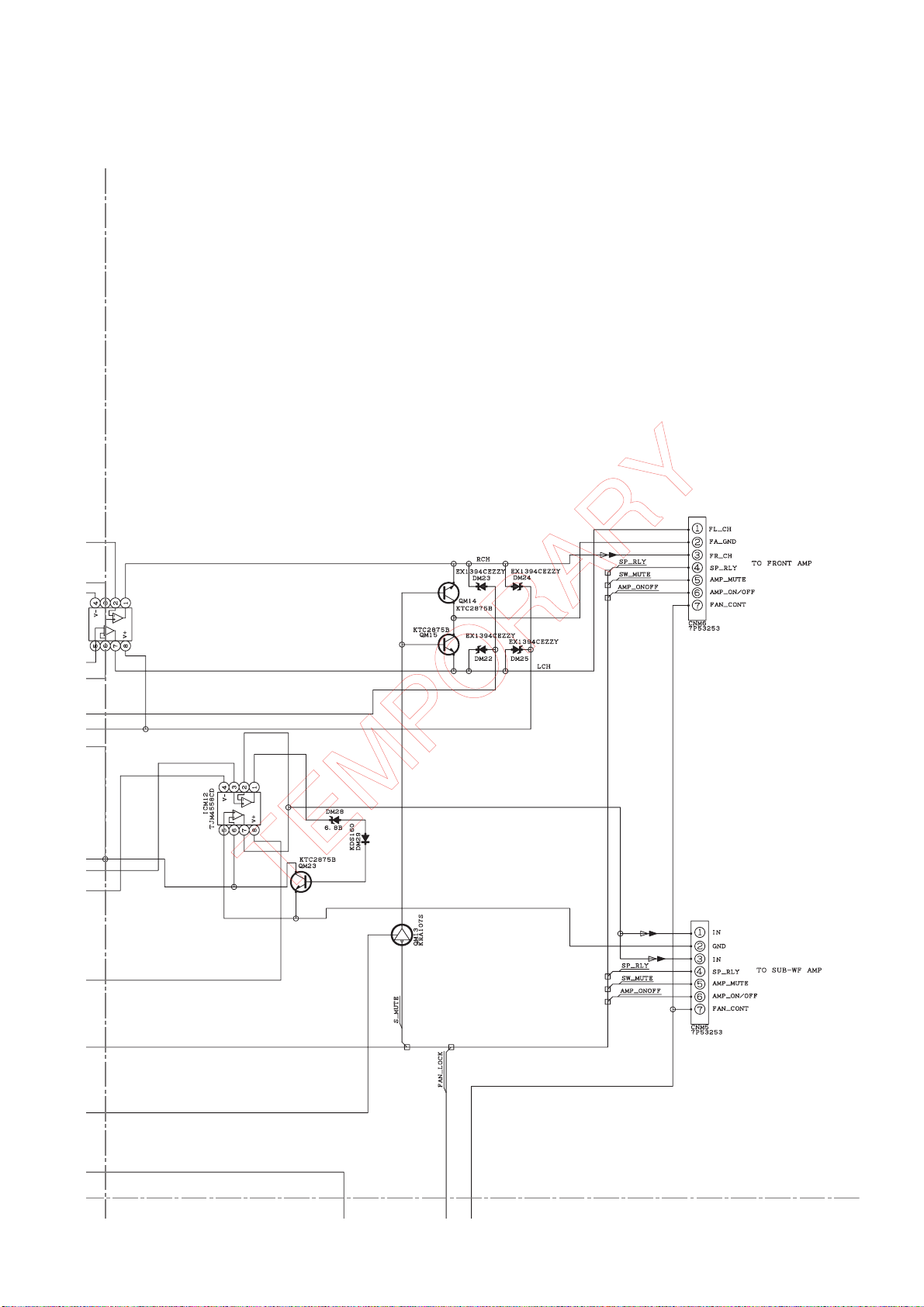
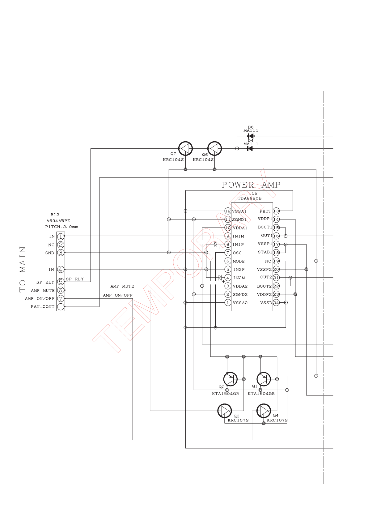
[4] Amplifier Block Diagram
C50
0.1/50V
C20
0.1/50V
8
Figure 4-13: AMPLIFIER BLOCK DIAGRAM (1/2)
4 – 13
Page 29
AN-GR500H
8
Figure 4-14: AMPLIFIER BLOCK DIAGRAM (2/2)
4 – 14
Page 30
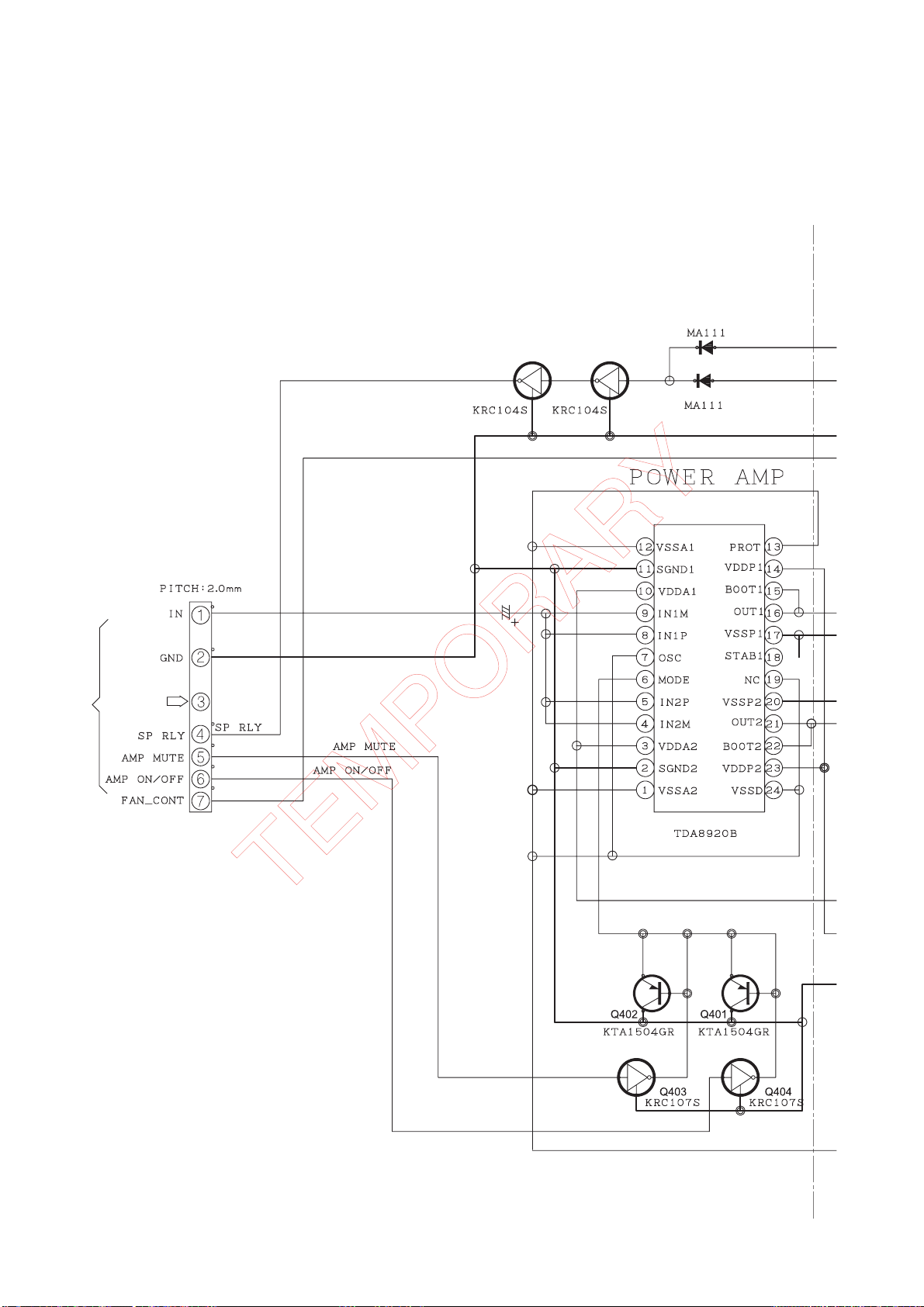
AN-GR500H
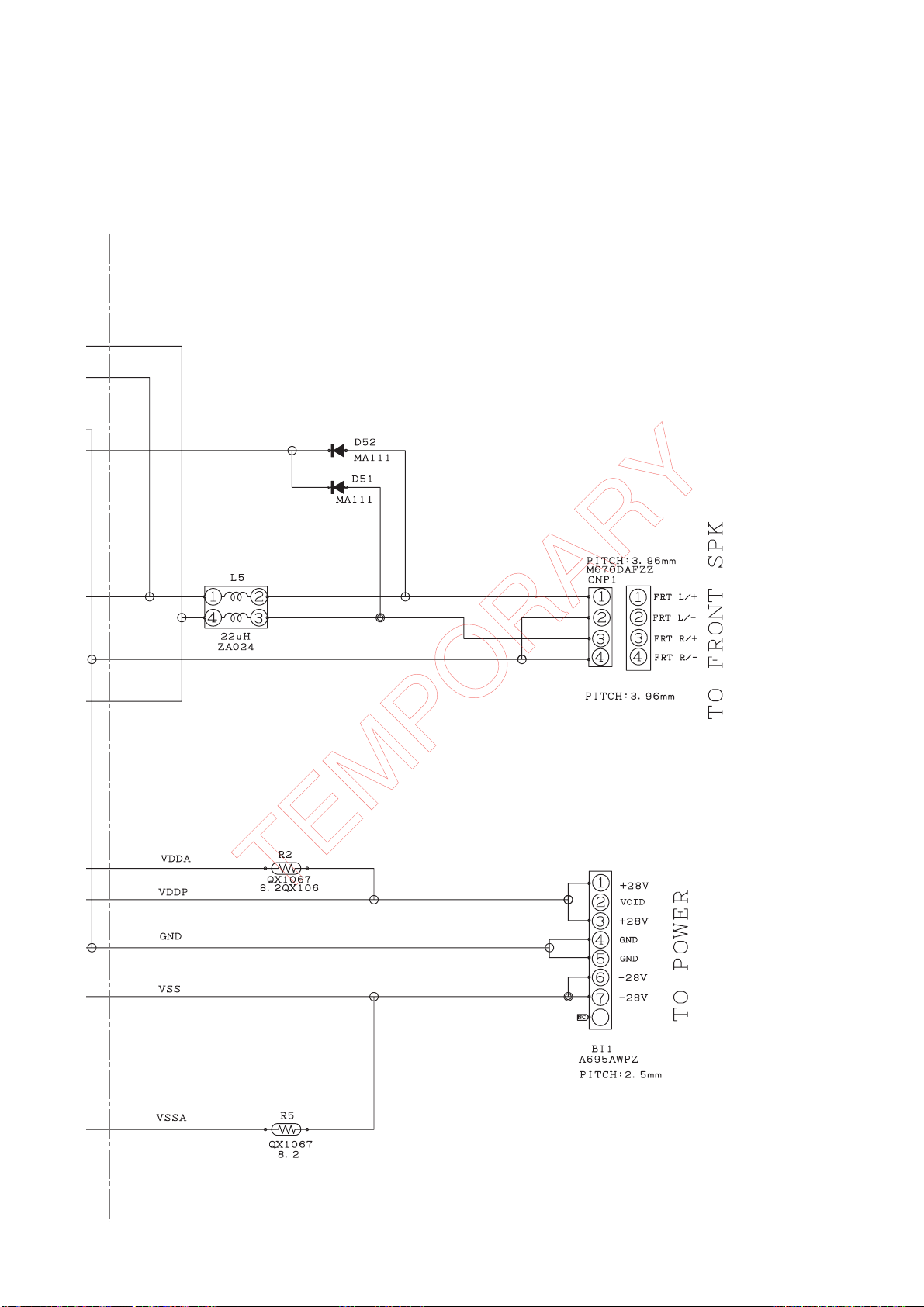
[5] Subwoofer Block Diagram
D406
TO
MAIN SECTION
Bi402
A696AWPZ
NC
Q407 Q406
C418
4.7/50V
D404
IC402
Figure 4-15: SUBWOOFER BLOCK DIAGRAM (1/2)
4 – 15
Page 31

D451
AN-GR500H
L405
R402
C439
0.015/
50V
C442
0.015/
50V
CNP401
QCNCMA045AW02
NC
TO
SUBWOOFER
R405
Figure 4-16: SUBWOOFER BLOCK DIAGRAM (2/2)
4 – 16
Bi403
A2393AWZZ
TO
NC
MAIN SECTION
Page 32

AN-GR500H
CHAPTER 5.
CHAPTER 5. CIRCUIT DESCRIPTION
[1] WAVEFORMS OF CD CIRCUIT
[1] To Check And Cancel Protect Circuit Detection
Line
1. After the power is turned on, the microprocessor (ICM7) built in this
model continuously monitors the following defective operation. If
any abnormality occurs, all power is shut down except in the microprocessor drive circuit.
1) An abnormal drop of each regulator output voltage.
(The protection circuit operates when the regulator output voltage is below 1.5 V.) The power is shut down immediately with
no display.
2) Defect of the cooling fan motor and the cooling fan drive circuit.
(Stoppage, etc.) The power is turned off after “FAN LOCK” is
displayed.
3) Over voltage or reduced voltage of power supply.
The power is shut down immediately with no display when voltage is abnormal.
2. Failure detection conditions of the built-in microprocessor, check of
the detection line and solution.
Conditions
1) To detect failure according to voltage of the microprocessor
ICM7 pin 91.
2) Abnormal if pulse signals are not input into the pin 5 (FAN
LOCK) for more than 5 seconds.
3) Abnormal if the voltage of the pin 97 (+B CHECK) is lower than
1.2 V or higher than 3.0 V.
1. Check of the detection line and solution
NOTE: If the microprocessor detects failures of 1), 2) and 3)
above, it does not operate protectively when its PROTECT,
and +B CHECK detection lines are disconnected.
When these failures are caused by output short-circuit of each
regulator, components and PWB of the regulator may burn
out. If the cause is not clear, do not disconnect the detection
line.
(Even if any failure is detected, conduction is available for 0.5
second. You can check conduction by an oscilloscope, etc.
However, a tester is not available due to rapid rise and decay
of voltage.)
1. When output voltage of each regulator drops abnormally.
Connect the oscilloscope to the regulated output of the regulator
and power on the system. If the voltage is significantly lower than
that shown in the circuit diagram (approx. 1.5 V or less), the regulator itself and the destination circuit are suspected.
5 – 1
Page 33

[2] Failure Detection Identification Using STANDBY LED
AN-GR500H
1. Identification format using STANDBY LED
If any failure is detected, STANDBY LED blinks red after power off
(see Fig. 1 below). You can identify the failure state by checking
which LED output number from the frame head is blinking 4 times
each for 2 seconds.
Fig. 1 shows the LED output No. 2. is blinking due to failure.
Power OFF
1 frame
3sec
2sec
No.1LED output
Alternate blinking for
failure detection
Red ON
500m 500m 500m 500m
2sec
No.2
2sec
3sec
3sec
2sec
No.3 No.6 No.7 No.1
3sec
Normally, LED light up for 2 seconds and light off for 1 second on a
3-second cycle (6 times from No. 1 to No. 6). For No.7, LED light off
for 3 seconds, showing the frame end (for recognition of the frame
head).
In No. 2, LED blinks alternately at shorter intervals than usual for failure identification. For failure status, refer to the appendix, “STAND-BY
LED Error Message”.
3sec
2sec
As shown in Fig. 1, LED alternately blinks due to failure on a
500-msec cycle with duty of 50%.
3sec
LED output
Figure 1
2. Failure detection
1. SYS-PROTECT detection: To detect failure of the power supply circuit (except the 1.8 V power supply circuit).
2. B_CHECK detection: To check timing at power ON/OFF and detect
over voltage and reduced voltage of the primary AC power after the
power is turned on.
3. AVCK detection: To detect failure of the 1.8 V power supply circuit
(AVCK1 and AVCK2).
4. AMP_SW_PROT detection: To detect failure in the subwoofer AMP.
3. STANDBY LED Error Message
No. Name of failure detection Solution
1 SYS-PROTECT detection Immediate power shut-down; Identification No.1 blinking
2 B_CHECK detection Immediate power shut-down; Identification No.2 blinking in case of over voltage
3 AVCK detection Immediate power shut-down; Identification No.3 blinking
4 AMP_SW_PROT detection Immediate power shut-down; Identification No.6 blinking
No blinking in case of reduced voltage
5 – 2
Page 34

AN-GR500H
[3] Waveforms Of SUBWOOFER Circuit
(at no signal)
2006/07/03
16
21
5 – 3
Page 35

[4] Voltage
AN-GR500H
5 – 4
Page 36

AN-GR500H
ICP100
ICM3
ICT1
ICM14
ICM17
ICM9
ICM8
Q1
Q2
Q3
Q4
ICM10
PIN NO. VOLTAGE (V) PIN NO. VOLTAGE (V)
1 1.63 41
2 0.00 42 0.00
3 1.63 43
4 0.00 44 3.13
5 1.67 45
6
7 0.00 47 1.52
8
9 0.00 49 0.00
10 1.66 50 1.62
11 0.00 51 0.00
12 1.48 52 1.65
13 1.49 53
14 3.14 54
15 0.00 55 0.00
16
17
18 0.00 58 0.00
19 0.00 59 0.00
20 0.00 60 0.00
21
22 3.10 62 3.12
23
24 4.72 64
25 4.72 65 1.65
26 0.00 66 3.11
27 2.29 67 3.11
28 2.29 68 3.12
29 2.24 69 3.13
30 2.25 70 3.12
31 2.29 71 2.62
32 2.30 72
33
34 4.72 74
35 2.30 75 1.65
36 2.91 76
37
38
39
40 4.73 80 3.12
PIN NO. VOLTAGE (V)
C 0.00
B 6.03
E 5.66
PIN NO. VOLTAGE (V)
C 0.00
B 4.73
E 5.25
PIN NO. VOLTAGE (V)
C 4.67
B 0.00
E 0.00
PIN NO. VOLTAGE (V)
C 5.64
B
E 0.00
0.00 46 3.13
0.00 48 1.52
0.00 56 0.00
0.00 57 0.00
0.00 61 3.12
0.00 63 0.00
0.00 73 2.62
0.00 77 0.00
0.00 78 3.12
0.00 79 0.00
0.00
0.00
0.00
0.00
0.00
0.00
0.00
0.00
0.00
0.00
PIN NO. VOLTAGE (V)
PIN NO. VOLTAGE (V)
PIN NO. VOLTAGE (V)
PIN NO. VOLTAGE (V) PIN NO. VOLTAGE (V)
1 0.67 15 0.00
2 0.54 16 2.58
3 1.51 17 2.53
4 1.51 18
5 1.51 19 3.20
6 3.11 20
7 0.00 21 3.14
8
9 3.12 23 3.22
10 0.90 24 1.62
11 0.60 25 1.60
12 0.70 26 0.00
13 0.70 27 1.53
14 0.00 28 1.59
PIN NO. VOLTAGE (V) PIN NO. VOLTAGE (V)
1 -31.28 21 -34.12
2 -31.29 22 -34.37
3 1.98 23 -34.36
4 0.00 24 -34.46
5 1.46 25
6 1.45 26
7 3.32 27 -34.37
8 3.31 28 -34.35
9 3.26 29 -34.36
10 0.12 30 -33.73
11 -34.45 31 -34.76
12 -34.22 32 -34.36
13 -34.43 33 -34.35
14 -34.41 34 -34.34
15 -34.65 35 -34.34
16 -34.42 36 -31.35
17 -34.46 37 -34.36
18
19 -34.46 39 -34.34
20
1 4.79
2
3 4.73
4
5 1.63
1 4.73
2 0.00
3 4.74
4
5 3.10
1 3.01
2 3.01
3
4 0.00
5 0.00
0.00
0.00
0.00
0.00
0.00 22 0.00
0.00 38 -31.56
0.00 40 -34.32
PIN NO. VOLTAGE (V)
1 2.30
2 2.33
3 4.80
4 0.00
5 2.36
6 2.29
7
8 2.43
9 2.22
10
11 4.74
12 4.75
13 4.74
14
15 4.84
16 3.22
PIN NO. VOLTAGE (V)
1
2
3 0.00
4 0.00
5 3.17
6 3.15
7 3.16
8 3.13
5 – 5
0.00
0.00
0.00
0.00
0.00
0.00
0.00
0.00
0.00
Page 37

AN-GR500H
ICM18
ICA1
ICM15
ICM5
ICM12
ICM11
ICM16
QM19
IC2
QP1Q6Q7
IC801
IC802
Q802
Q803
IC803
IC804
Q804
IC800
PIN NO. VOLTAGE (V)
1
2
3
4 -8.94
5
6
7
8 8.73
PIN NO. VOLTAGE (V)
1
2
3
4 -8.93
5
6 0.00
7 0.00
8 8.60
PIN NO. VOLTAGE (V)
1 4.89
2
3 4.90
4
5 0.00
6
7
8
9 0.00
10 8.59
11 4.90
12 4.80
13
14 4.91
PIN NO. VOLTAGE (V)
1
2 0.95
3 3.12
4 0.00
5
6 0.00
7 0.00
8 3.12
0.00
0.00
0.00
0.00
0.00
0.00
0.00
0.00
0.00
0.00
0.00
0.00
0.00
0.00
0.00
0.00
0.00
0.00
PIN NO. VOLTAGE (V) PIN NO. VOLTAGE (V)
1
2 1.52 2
3 1.65 3 25.89
4 1.02 4
5 1.58 5 0.00
6 0.00 6 5.23
7 3.12 7 -22.91
8
9 0.00 9 0.00
10 2.61 10 25.86
11 2.61 11
12
13 2.28 13 -17.84
14 0.00 14 26.14
15 0.00 15 10.36
16 4.73 16 -0.11
17 0.00 17 -25.95
18 1.09 18 -13.81
19 1.05 19 -25.76
20 1.09 20 -25.96
21 1.14 21 -0.13
22 0.84 22 10.38
23 0.84 23 26.14
24 0.83 24 -25.77
25 0.82
26 0.82
27 0.80
28 0.80
PIN NO. VOLTAGE (V)
1 9.16
2
3 3.12
PIN NO. VOLTAGE (V)
1 0.00
2 3.12
3 1.64
4 2.22
5 0.00
PIN NO. VOLTAGE (V)
C 1.66
B 2.49
E 3.15
0.00 1 -25.77
0.00
0.00
0.00 8 0.00
0.00
0.00 12 -25.76
0.00
PIN NO. VOLTAGE (V)
1 0.40
2 1.11
3 2.05
4
5 0.96
6 10.39
7 1.69
8 0.29
PIN NO. VOLTAGE (V)
1 16.68
2
3 2.46
PIN NO. VOLTAGE (V)
1 3.87
2
3 8.08
PIN NO. VOLTAGE (V)
1 14.61
2
3 4.97
PIN NO. VOLTAGE (V)
1
2
3 9.00
PIN NO. VOLTAGE (V)
C
B 0.68
E
PIN NO. VOLTAGE (V)
C
B 9.82
E -9.21
0.00
0.00
0.00
0.00
14.61
0.00
0.00
0.00
0.00
PIN NO. VOLTAGE (V)
C 0.00
B 30.53
E 0.00
PIN NO. VOLTAGE (V)
C 3.33
B 0.00
E
0.00
5 – 6
PIN NO. VOLTAGE (V)
D 389.54
G
S
PIN NO. VOLTAGE (V)
C 2.95
B
E 0.00
0.62
0.00
0.00
Page 38

AN-GR500H
IC402 Q402
PIN NO. VOLTAGE (V) PIN NO. VOLTAGE (V)
1 -25.90 C0.00
20.00 B4.70
3 26.00 E5.20
40.00
50.00
65.20
7 -22.50 PIN NO. VOLTAGE (V)
80.00 C5.10
90.00 B0.00
10 26.00 E0.00
11 0.00
12 -25.90
13 -17.80
14 26.30 PIN NO. VOLTAGE (V)
15 10.70 C3.10
16 -0.10 B0.00
17 -26.10 E0.00
18 -13.60
19 -25.90
20 -26.10
21 -0.10
22 10.80
23 26.20
24 -25.90
PIN NO. VOLTAGE (V)
PIN NO. VOLTAGE (V)
PIN NO. VOLTAGE (V)
Q401
C0.00
B5.20
E5.60
Q403
C4.70
B0.00
E0.00
Q406
C0.00
B8.60
E0.00
Q404
Q407
5 – 7
Page 39

AN-GR500H
CHAPTER 6. CIRCUIT SCHEMATICS AND PARTS LAYOUT
[1] Notes On Schematic Diagram
• Resistor:
To differentiate the units of resistors, such symbol as
K and M are used: the symbol K means 1000 ohm
and the symbol M means 1000 kohm and the resistor without any symbol is ohm-type resistor.
Besides, the one with “Fusible” is a fuse type.
• Capacitor:
To indicate the unit of capacitor, a symbol P is used:
this symbol P means pico-farad and the unit of the
capacitor without such a symbol is microfarad. As to
electrolytic capacitor, the expression “capacitance/
withstand voltage” is used.
(CH), (TH), (RH), (UJ): Temperature compensation
(ML): Mylar type
(P.P.): Polypropylene type
REF. NO DESCRIPTION POSITION
SW1 ON/STAND-BY ON-OFF
SW2 VOLUME DOWN ON-OFF
SW3 VOLUME UP ON-OFF
SW4 FUNCTION ON-OFF
• Schematic diagram and Wiring Side of P.W.Board
for this model are subject to change for
improvement without prior notice.
• The indicated voltage in each section is the one
measured by Digital Multimeter between such a
section and the chassis with no signal given.
1. In the tuner section,
indicates FM stereo
• Parts marked with “ “ ( ) are
important for maintaining the safety of the set. Be
sure to replace these parts with specified ones for
maintaining the safety and performance of the set.
[2] Types Of Transistor And LED
TOP VIEW
FRONT
VIEW
B C E
2SA2012
1 23
KTC4375Y
SARS03
1. Anode
2. No Contact
3. Cathode
FRONT
VIEW
B C E
KTA1046Y
STH102CF
FRONT
VIEW
E C B
(S)(G)(D)
(1)(2)(3)
KTA1266 GR
KTA1023Y
KTC3199 GR
PST3229N
TOP VIEW
KDS226
KDS184
B
(3)
E
(1)
KRC107S
KRC101S
KRA107S
KRC104S
KTC3875 GR
KTA1504 GR
KTC2875B
6206P39T
FRONT
AC AC
TS10B05G
TS20P05G
TS6P05G
TOP
VIEW
VIEW
C
(2)
TOP VIEW
1N404S
1N4148H
DRL204F
1N4004
KDS160
MA111
Green
Cathode
A309SGM2E7
D1SS119
Red
Cathode
Anode
6 – 1
Page 40

AN-GR500H
[3] Schematic Diagram
MAIN PWB-A1
AUDIO SIGNAL
LUGM2
DM31
KDS226
CM107(0.1)
Figure 6-1: MAIN SCHEMATIC DIAGRAM (1/8)
6 – 2
Page 41

AN-GR500H
Figure 6-2: MAIN SCHEMATIC DIAGRAM (2/8)
6 – 3
Page 42

AN-GR500H
ICM10
Figure 6-3: MAIN SCHEMATIC DIAGRAM (3/8)
6 – 4
Page 43

AN-GR500H
TO
FRONT AMP
TO
SUBWOOFER AMP
Figure 6-4: MAIN SCHEMATIC DIAGRAM (4/8)
6 – 5
Page 44

AN-GR500H
TO TUNER PACK
Figure 6-5: MAIN SCHEMATIC DIAGRAM (5/8)
6 – 6
TO INTERFACE PWB
CM282
100pF
CM280
(100P)
CM283 (100P)
CM281 (100P)
Page 45

AN-GR500H
Figure 6-6: MAIN SCHEMATIC DIAGRAM (6/8)
6 – 7
FOR REFLASH ONLY
Page 46

AN-GR500H
Figure 6-7: MAIN SCHEMATIC DIAGRAM (7/8)
6 – 8
Page 47

AN-GR500H
Figure 6-8: MAIN SCHEMATIC DIAGRAM (8/8)
6 – 9
TO
POWER SECTION
Page 48

AN-GR500H
TO
POWER PWB-B1
MAIN SECTION
TO
DISPLAY SECTION
TO
DIGITAL AMP
Figure 6-9: POWER SCHEMATIC DIAGRAM (1/2)
6 – 10
Page 49

A028AW
AN-GR500H
AN-GR500H
0.0033/AC250V
KZA136WJ
0.0033/AC250V
KZA136WJ
AC 220 - 240V ~ 50Hz
Europe QACCE0002AW00
Figure 6-10a: POWER SCHEMATIC DIAGRAM (2/2)
6 – 11
Page 50

AN-GR500H
AN-GR500H
For U.K., Australia and New Zealand
A028AW
0.0033/AC250V
KZA136WJ
0.0033/AC250V
KZA136WJ
AC 220 - 240V ~ 50Hz
AUSTRALIA/NEW ZEALAND
U.K.
Figure 6-10b: POWER SCHEMATIC DIAGRAM (2/2)
6 – 12
QACCLA002AW00
QACCBA005AW00
Page 51

-MEMO-
AN-GR500H
6 – 13
Page 52

AN-GR500H
DISPLAY PWB-B2
FL100
1000P
CP10
100P
ICP100
270P
1000P
Figure 6-11: DISPLAY SCHEMATIC DIAGRAM (1/2)
6 – 14
Page 53

AN-GR500H
TO
INTERFACE PWB
TO
INTERFACE PWB
Figure 6-12: DISPLAY SCHEMATIC DIAGRAM (2/2)
6 – 15
Page 54

AN-GR500H
AMPLIFIER PWB-C
AUDIO SIGNAL
TO MAIN SECTION
Figure 6-13: AMP SECTION (FRONT) SCHEMATIC DIAGRAM (1/2)
6 – 16
Page 55

AN-GR500H
TO SPEAKER SECTION
TO POWER SECTION
Figure 6-14: AMP SECTION (FRONT) SCHEMATIC DIAGRAM (2/2)
6 – 17
Page 56

AN-GR500H
SUBWOOFER PWB-D
A
B
C
D
AUDIO SIGNAL
FROM MAIN SECTION
E
F
G
H
1
23456
Figure 6-15: SUBWOOFER SCHEMATIC DIAGRAM (1/2)
6 – 18
Page 57

AN-GR500H
TO
SUBWOOFER
FROM
POWER SECTION
7
8 9 10 11 12
Figure 6-16: SUBWOOFER SCHEMATIC DIAGRAM (2/2)
6 – 19
Page 58

AN-GR500H
FRONT
SWF
[4] Charts Of Connecting Wires
A
LUG01
CNS402
B
C
D
E
LUG01
INTERFACE PWB-B3
11
ANALOG IN
AUDIO
DR
AUDIO
DIGITAL IN
CNS1
CNS02
YGKBYGKBY
YGKBYG
K
KB
B
GKB
131
FRONT
A
8
SWF
CNS801
F
G
H
ANTENNA
75 Ohms
1
4
23456
Figure 6-17: WIRING CONNECTION (1/2)
6 – 20
Page 59

AN-GR500H
CNS402
CNS403
7
Bi402Bi403
17
17
WH
GY
WH
GY
WH
GY
CNP401
CNS401
CNS01
BK
BK
BK
BK
CNW800-B
CNW800-A
7
8 9 10 11 12
Figure 6-18: WIRING CONNECTION (2/2)
6 – 21
Page 60

AN-GR500H
[5] Wiring Side Of PWB
A
B
C
D
MAIN PWB-A1
E
F
G
LINE 3 LINE 2
LINE 1
COAXIAL
OPTICAL-2 OPTICAL-1
AUDIO-ANALOG IN AUDIO-DIGITAL IN
H
1
23456
Figure 6-19: WIRING SIDE OF MAIN PWB (TOP VIEW) (1/2)
6 – 22
Page 61

AN-GR500H
Lead-free solder indication
Lead-free solder is used in the MAIN PWB.
Refer to "Precautions for handling lead-free solder" for instructions
and precautions.
7
8 9 10 11 12
Figure 6-20: WIRING SIDE OF MAIN PWB (TOP VIEW) (2/2)
6 – 23
Page 62

AN-GR500H
A
MAIN PWB-A1
B
CM282
CM281
RM268
RM269
C
CM283
CM280
D
E
F
G
Lead-free solder indication
Lead-free solder is used in the MAIN PWB.
Refer to "Precautions for handling lead-free solder" for instructions
H
and precautions.
1
23456
Figure 6-21: WIRING SIDE OF MAIN PWB (BOTTOM VIEW) (1/2)
6 – 24
Page 63

AN-GR500H
7
8 9 10 11 12
Figure 6-22: WIRING SIDE OF MAIN PWB (BOTTOM VIEW) (2/2)
6 – 25
Page 64

AN-GR500H
AN-GR500H
A
B
POWER PWB-B1
C
D
E
F
G
H
1
23456
Figure 6-23a: WIRING SIDE OF POWER PWB (TOP VIEW) (1/2)
6 – 26
Page 65

AN-GR500H
A
AN-GR500H
For U.K., Australia and New Zealand
POWER PWB-B1
B
C
D
E
F
G
H
1
23456
Figure 6-23b: WIRING SIDE OF POWER PWB (TOP VIEW) (1/2)
6 – 27
Page 66

AN-GR500H
Lead-free solder indication
Lead-free solder is used in the POWER PWB.
Refer to "Precautions for handling lead-free solder" for instructions
and precautions.
7
8 9 10 11 12
Figure 6-24: WIRING SIDE OF POWER PWB (TOP VIEW) (2/2)
6 – 28
Page 67

-MEMO-
AN-GR500H
6 – 29
Page 68

AN-GR500H
A
B
C
D
POWER PWB-B1
E
F
G
Lead-free solder indication
Lead-free solder is used in the POWER PWB.
Refer to "Precautions for handling lead-free solder" for instructions
H
and precautions.
1
23456
Figure 6-25: WIRING SIDE OF POWER PWB (BOTTOM VIEW) (1/2)
6 – 30
Page 69

AN-GR500H
7
8 9 10 11 12
Figure 6-26: WIRING SIDE OF POWER PWB (BOTTOM VIEW) (2/2)
6 – 31
Page 70

AN-GR500H
A
B
C
D
DISPLAY PWB-B2
E
F
G
Lead-free solder indication
Lead-free solder is used in the DISPLAY PWB.
Refer to "Precautions for handling lead-free solder" for instructions
H
and precautions.
1
23456
Figure 6-27: WIRING SIDE OF DISPLAY PWB (TOP VIEW)
6 – 32
Page 71

AN-GR500H
A
B
C
D
DISPLAY PWB-B2
E
F
G
Lead-free solder indication
Lead-free solder is used in the DISPLAY PWB.
Refer to "Precautions for handling lead-free solder" for instructions
H
and precautions.
1
23456
Figure 6-28: WIRING SIDE OF DISPLAY PWB (BOTTOM VIEW)
6 – 33
Page 72

AN-GR500H
A
B
C
D
INTERFACE PWB-B3
CP25
(0.7µ)
E
F
G
Lead-free solder indication
Lead-free solder is used in the INTERFACE PWB.
Refer to "Precautions for handling lead-free solder" for instructions
and precautions.
H
1
23456
Figure 6-29: WIRING SIDE OF INTERFACE PWB
6 – 34
Page 73

AN-GR500H
A
AMPLIFIER PWB-C
B
C
D
E
F
G
Lead-free solder indication
Lead-free solder is used in the AMPLIFIER PWB.
Refer to "Precautions for handling lead-free solder" for instructions
H
and precautions.
1
23456
Figure 6-30: WIRING SIDE OF AMPLIFIER PWB (TOP VIEW)
6 – 35
Page 74

AN-GR500H
A
AMPLIFIER PWB-C
B
C
D
E
F
G
Lead-free solder indication
Lead-free solder is used in the AMPLIFIER PWB.
Refer to "Precautions for handling lead-free solder" for instructions
H
and precautions.
1
23456
Figure 6-31: WIRING SIDE OF AMPLIFIER PWB (BOTTOM VIEW)
6 – 36
Page 75

AN-GR500H
A
B
C
D
SUBWOOFER PWB-D
1 2 3 4 5678
E
12345678
F
G
Lead-free solder indication
Lead-free solder is used in the SUBWOOFER PWB.
Refer to "Precautions for handling lead-free solder" for instructions
H
and precautions.
1
23456
Figure 6-32: WIRING SIDE OF SUBWOOFER PWB (TOP VIEW)
6 – 37
Page 76

AN-GR500H
A
B
C
D
SUBWOOFER PWB-D
E
F
G
Lead-free solder indication
Lead-free solder is used in the SUBWOOFER PWB.
H
Refer to "Precautions for handling lead-free solder" for instructions
and precautions.
1
23456
Figure 6-33: WIRING SIDE OF SUBWOOFER PWB (BOTTOM VIEW)
6 – 38
Page 77

AN-GR500H
CHAPTER 7. OTHERS
[1] Function Table Of IC
ICM7 RH-IXA225AW00: System Microcomputer ( IXA225AW ) (1/3)
Device Pin No. Terminal Name Port Name Input/Output Function
D-IN SW 1 FUNC_DIG3 P96/ANEX1 Output DIR_RXP2 : COAXIAL(Coaxial) ="H" OTHER="L"
2 FUNC_DIG2 P95/ANEX0 Output DIR_RXP1 : DIN2(Optical2) ="H" OTHER="L"
3 FUNC_DIG1 P94 Output DIR_RXP0 : DIN1(Optical1) ="H" OTHER="L"
(RESERVE) 4 FUNC_ANA P93 Output Analog Function ="H", OTHER ="L"
FAN 5 FAN_LOCK P92/TB2IN Input [TB2IN]FAN PULSE DETECTING FOR ERROR
POWER 6 SYS_STOP P91/TB1IN Input [TB1IN]AC Power Fail Detection.Change Micom
Operation Mode, H → L ( LOW→STOP Mode )
(RESERVE) 7 NC P90/TB0IN Output
8 BYTE BYTE Input Connect to VSS
9 CNVSS CNVSS Input Using Single Chip Mode. Connect Pull-Down
10 XCIN P87/XCIN Input SUB CLOCK IN. Connect to 32.768KHz X'tal
11 XCOUT P86/XCOUT Output SUB CLOCK OUT. Connect to 32.768KHz X'tal
(µcom) 12 RESET RESET Input MICOM IC RESET input. Active "L".
13 X_OUT XOUT Output MAIN CLOCK OUT. 8.3886MHz Ceramic
14 GND VSS — Connect to GND (VSS)
15 X_IN X_IN Input MAIN CLOCK IN. 8.3886MHz Ceramic Resonator
16 VCC VCC1 Input Micom Supply Input (3.3V). Back-up Supply
17 NMI P85/NMI Input Connect Pull-UP Resistor to VCC.
AMP 18 NC P84/INT2 Output
19 NC P83/INT1 Output
(RESERVE) 20 NC P82/INT0 Output
21 NC P81 Output
ENHANCER 22 ENH_MRREQ P80 Input AUDISTRY MRREQ L : Normal /H : Communica-
DIR 23 DIR_GPO0 P77 Input DIR Output Port monitor, Output Setting Depend
24 DIR_GPO1 P76 Input DIR Output Port monitor, Output Setting Depend
25 DIR_RESET P75/TA2IN Output DIR IC RESET H : Normal Operation L : RESET
26 DB_SCP_BSY P74/TA2OUT Input DOLBY IC(OPTION)
DIR 27 DB_SCP_IRQ P73/CTS2/RTS2/TA1IN Input [TA1IN]DOLBY IC(OPTION), EDGE Detection
ENHANCER 28 DOLBY_RESET P72/CLK2/TA1OUT Output RESET
A-S.W&ADC 29 DIR_SCL/AD_SCL/
30 DIR_SDA/
31 FLASH_TXD/
FLASH/
FLD
DOLBY 35 DB_SDA P63/TXD0/SDA0 Input / Output [I2Cbus]DOLBY IC MICOM IF DATA I/O
ENHANCER 37 ENH_RSTB P61/CLK0 Output AUDISTRY reset
(µcom) 39 OSC_OUT P57/CLKOUT Output For Checking Freq. Generate.
ENHANCER 40 ENH_BUSY P56/ALE Input AUDISTRY I2CBUSY Output L : Normal /H : Busy
FLASH 41 FLASH_EPM P55 Input Connect Pull-Down Resistor to VSS.
EEPROM 42 EEP_SDA P54 Output [softI2C]EEPROM DATA I/O
FLASH 46 FLASH_CE P50 Input Connect Pull-Down Resistor to VSS.
VOLUME IC 48 SW_VOL_CLK P46 Output Volume IC Clock
32 FLASH_RXD P66/RXD1/SCL1 Input FLASH Writer Send Data Input
33 FLASH_SCLK/
34 FLASH_BUSY/
36 DB_SCL P62/RXD0/SCL0 Output [I2Cbus]DOLBY IC MICOM IF CLOCK
38 ENH_PWDB P60/CTS0/RTS0 Output AUDISTRY Power Down
43 EEP_SCL P53 Output [softI2C]EEPROM CLOCK OUTPUT
44 NC P52 Output
45 EEP-WP P51 Output EEPROM WRITE_PROTECT H i-Z : Protect
47 NC P47 Output
49 SW_VOL_DATA P45 Output Volume IC Data
ENH_SCL
AD_SDA/
ENH_SDA
FLD DATA
FLD SCK
FLD CS
P71/RXD2/SCL2/TA0IN
(note 1)
P70/TXD2/SDA2/
TA0OUT (note 1)
P67/TXD1/SDA1 Output FLASH Writer Send Data Output/FL Driver
P65/CLK1 Output FLASH Writer Clock Input/FL Driver R8A66021GP
P64/CTS1/RTS1/CTS0/
CLKS1
Output [I2Cbus]DIR/ADC&ANALOG SW/ENHANCER
Input/Output [I2Cbus]DIR/ADC&ANALOG SW/ENHANCER
Output FLASH Writer BUSY Output. BUSY : “H”/ FL Driver
Resistor to VSS.
Resonator
tion Error
on Command to DIR.
on Command to DIR.
MICOM IF Clock (note 1)Nch Open Drain
MICOM IF Data I/O (note 1)Nch Open Drain
R8A66021GP Display Data Output
Serial Clock Output.
R8A66021GP CS Control Output
Writing Zone Invalid / L : Writing Enable.
7 – 1
Page 78

AN-GR500H
ICM7 RH-IXA225AW00: System Microcomputer ( IXA225AW ) (2/3)
Device Pin No. Terminal Name Port Name Input/Output Function
FLD 50 FLD RESET P44 Output FL Driver R8A66021GP Reset Output
51 AMP_SW_PROT P43 I_PU AMP Abnormal Detection H : Normal, L : Abnormal
Detect (AMP_SP_RELAY=While High Enable)
52 NC P42 Output
53 NC P41 Output
54 NC P40 Output
55 NC P37 Output
AMP 56 NC P36 Output
57 AMP_SP_RELAY P35 Output SPEAKER Relay Control Output, H: Relay ON
L:Relay OFF
58 NC P34 Output
59 S_MUTE P33 Output SYSTEM MUTE Control Output, Pre AMP Mute
H : MUTE OFF L : MUTE ON
60 AMP_SW_PWR_DWNP32 Output AMP Power Down H : Standby, L : Operate
61 AMP_SW_MUTE P31 Output AMP MUTE Control Output, L : MUTE OFF
H : MUTE ON
(µcom) 62 VCC VCC2 Input Micom Supply Input (3.3V). Back-up Supply
63 NC P30 Output
(µcom) 64 GND VSS — Connect to GND (VSS).
65 NC P27 Output
66 NC P26 Output
67 NC P25 Output
68 NC P24 Output
69 NC P23 Output
(RESERVE) 70 NC P22 Output
71 NC P21 Output
72 NC P20 Output
73 NC P17 Output
74 NC P16/INT4 Output
REMOTE 75 RX-IN P15/INT3 Input [INT]SHARP Format, Remote Control Input.
76 NC P14 Output
RDS 77 RDS RDY P13 Input RDS READY INPUT
78 RDS CLK P12 Output RDS CLOCK OUTPUT
79 RDS RST P11 Output RDS RAM RESET
80 RDS DO P10 Input RDS DATA INPUT
LED-SINGLE 81 TIMER_LED P07/AN0_7 Output TIMER LED (Standby) Contorl Port
POWER 82 AVCK1 P06/AN0_6 Input [AD]D1.8V Abnormal Voltage Detection
83 AVCK2 P05/AN0_5 Input [AD]A1.8V Abnormal Voltage Detection
KEY 84 KEY_FUNCTION P04/AN0_4 Input Function Change Key Input
TUNER 85 CCB_DO P03/AN0_3 Input Serial Data Input from SANYO CCB Device
86 CCB_CL P02/AN0_2 Output Serial Clock Output from SANYO CCB Device.
87 CCB_DI P01/AN0_1 Output Serial Command Data Output from SANYO CCB
Device
88 CCB_CE P00/AN0_0 Output CE Control Output from SANYO CCB Device
MODEL 89 NC P107/AN7/KI3 Input
AREA 90 AREA P106/AN6/KI2 Input For Destination Detection
POWER 91 SYS-PROTECT P105/AN5/KI1 Input [A/D] SYS Abnormal Supply Detection.
KEY 92 KEY_POWER P104/AN4/KI0 Input Power Key Input (POWER)
93 KEY1 P103/AN3 Input [A/D]Unit Key Input
(RESERVE) 94 MP_SW P102/AN2 Output Micom Power Select 1:OFF 0:ON
95 TUNER_SM P101/AN1 Input TUNER IF SIGNAL MONITOR
(µcom) 96 GND AVSS — [A/D] VSS Reference. Connect to GND (VSS).
POWER 97 B_CHECK P100/A0 Input [A/D]
(µcom) 98 VREF VREF Input [A/D] Base Reference Voltage Input.
(µcom) 99 AVCC AVCC Input [A/D] Reference Supply Input.
POWER 100 POWER P97/ADTRG Output MAIN POWER CONTROL OUTPUT, H : POWER
ON L : POWER OFF
7 – 2
Page 79

ICM7 RH-IXA225AW00: System Microcomputer ( IXA225AW ) (3/3)
P96/ANEX1
0
P92/TB2IN
A
C
D
A
A
A
P57/RDY
/C
OU
A
FLASH
SCLK/F
LD SCK
POWER
AVC C
VREF
B_CHECK
GND
TUNER_SM
MP_SW
KEY1
KEY_POWER
SYS-PROTECT
FUNC_DIG3 1
FUNC_DIG2
FUNC_DIG1
FUNC_ANA
FAN_LOCK
SYS_STOP
BYTE
CNVSS
XCIN
XCOUT
RESET
X_OUT
GND
X_IN
VCC
ENH_MRREQ
DIR_GPO0
DIR_GPO1
DIR_RESET
DB_SCP_BSY
DB_SCP_IRQ
DOLBY_RESET
DIR_SCL/AD_S
L/ENH_SCL
DIR_SDA/AD_S
/ENH SD
AREANCCCB_CE
99989796959493929190898887868584838281
100
/SIN4
VREF
AVC C
P97/ADTRG
/SOUT4
P95/ANEX
2
/CLK4
P94/DA1
3
/TB4IN
P93/DA0
4
/TB3IN
5
/SOUT3
P91/TB1IN
6
/SIN3
NC 7
NMI
NC
NC
NC
NC
P90/TB0IN
/CLK3
8 BYTE P17/D15/INT5 73 NC
9 CNVSS P20/A7(/D0/-) 72 NC
10 P87/XCIN P21/A7(/D1/D0) 71 NC
11 P86/XCOUT P22/A7(/D2/D1) 70 NC
12 RESET P23/A7(/D3/D2) 69 NC
13 XOUT P24/A7(/D4/D3) 68 NC
14 VSS P25/A7(/D5/D4) 67 NC
15 XIN P26/A7(/D6/D5) 66 NC
16 VCC P27/A7(/D7/D6) 65 NC
17 P85/NMI VSS 64 GND
18 P84/INT2 P30/A8(/-/D7) 63 NC
19 P83/INT1 VCC 62 VCC
20 P82/INT0 P31/A9 61 AMP_SW_MUTE
21 P81/TA4IN/U P32/A10 60
22 P80/TA4OUT/U P33/A11 59 S_MUTE
23 P77/TA3IN P34/A12 58 NC
24 P76/TA3OUT P35/A13 57 AMP_SP_RELAY
25 P75/TA2IN/W P36/A14 56 NC
26 P74/TA2OUT/W P37/A15 55 NC
P73/CTS2/RTS2
27 P40/A16 54 NC
TA1IN/V
P72/CLK2
28
TA1OUT/V
P71/RXD2/SCL
29
TA0IN/TB5IN
P70/TXD2/SD
30
TA0OUT
AVS S
P100/AN0
P101/AN1
P102/AN2
P103/AN3
P104/AN4/KI0
P105/AN5/KI1
P106/AN6/KI2
IXA225AW
CCB_DI
CCB_CL
CCB_DO
P00/D0
P01/D1
P02/D2
P03/D3
P107/AN7/KI3
KEY_FUNCTIO
N
AVC K2
AVC K1
P04/D4
P05/D5
P06/D6
TIMER_LED
P07/D7
P10/D8 80
P11/D9 79
P12/D10 78 RDS CLK
P13/D11 77 RDS RDY
P14/D12 76
P15/D13/INT3 75 RX-IN
P16/D14/INT4 74 NC
P41/A17 53
P42/A18 52
P43/A19 51
RDS DO
RDS RST
NC
MP_SW_PWR_
DWN
NC
NC
AMP_SW_PROT
AN-GR500H
T
P64/CTS1/RTS1
P66/RXD1
P65/CLK1
_
FLASH_RXD
FLASH_BUSY/F
/CTS0/CLKS1
LD CS
P67/TXD1
3132333435
D DAT
FLASH_TXD/FL
P63/TXD0
P62/RXD0
363738394041424344454647484950
DB_SCL
DB_SDA
P60/CTS0/RTS0
P61/CLK0
ENH_RSTB
ENH_PWDB
LK
P56/ALE
OSC_OUT
ENH_BUSY
P55/HOLD
P54/HLDA
P53/BCLK
EEP_SCL
EEP_SDA
FLASH_EPM
P52/RD
NC
P51/WRH/BHE
P50/WRL/WR
EEP-WP
FLASH_CE
P47/CS3
P46/CS2
NC
SW_VOL_CLK
P45/CS1
SW_VOL_DATA
P44/CS0
FLD RESET
Figure 7-1 BLOCK DIAGRAM OF IC
7 – 3
Page 80

AN-GR500H
ICA1 VHiWM8775++-1: A/D Convertor (WM8775)
Pin No. Terminal Name Input/Output Function
1 AIN1L Input Channel 1 left input multiplexer virtual ground.
2 BCLK Input/Output ADC audio interface bit clock.
3 MCLK Input Master ADC clock: 256, 384, 512 or 768 fs (fs = Word clock frequency).
4 DOUT Output ACC data output.
5 ADCLRC Input/Output ADC left/right word clock.
6 DGND — Digital negative power supply.
7 DVDD — Digital positive power supply.
8 MODE Input Serial interface mode select.
9 CE Input Serial interface latch signal.
10 DI Input/Output Serial interface data.
11 CL Input Serial interface clock.
12* NC — No connection.
13 VMIDADC Output ADC mid-rail divider decoupling pin: 10 µF external decoupling.
14 ADCREFGND — ADC negative power supply and PWB connection.
15 ADCREFP Output ADC positive reference decoupling pin: 10 µF external decoupling.
16 AVDD — Analog positive power supply.
17 AGND — ADC negative power supply and PWB connection.
18 AINVGR Input Right channel multiplexer ground.
19 AINOPR Output Right channel multiplexer output.
20 AINVGL Input Left channel multiplexer ground.
21 AINOPL Output Left channel multiplexer output.
22 AIN4R Input Channel 4 right input multiplexer ground.
23 AIN4L Input Channel 4 left input multiplexer ground.
24 AIN3R Input Channel 3 right input multiplexer ground.
25 AIN3L Input Channel 3 left input multiplexer ground.
26 AIN2R Input Channel 2 right input multiplexer ground.
27 AIN2L Input Channel 2 left input multiplexer ground.
28 AIN1R Input Channel 1 right input multiplexer ground.
In this unit, the terminal with asterisk mark (*) is (open) terminal which is not connected to the outside.
AIN1L
BCLK
MCLK
DOUT
ADCLRC
DGND
DVDD
MODE
CE
DI
CL
NC
VMIDADC
ADCREFGND
1
2
3
4
5
6
7
8
9
10
11
12
13
14
28
27
26
25
24
23
22
21
20
19
18
17
16
15
AIN1R
AIN2L
AIN2R
AIN3L
AIN3R
AIN4L
AIN4R
AINOPL
AINVGL
AINOPR
AINVGR
AGND
AVDD
ADCREFP
Figure 7-2 BLOCK DIAGRAM OF IC
7 – 4
Page 81

AN-GR500H
A
ICM3 VHiCS8416CN-1: DIR (CS8416CN)
Pin No. Terminal Name Function
1* RXP3
2RXP2
3RXP1
4RXP0
5RXN
6 VA Analog power supply (Input) - Analog power supply. + 3.3 V normally.
7 AGND Analog ground (Input) - Ground for chip analog circuit.
8 FILT PLL loop filter (Output) - RC network is connected between this pin and the analog ground.
9 RST Reset (Input) - When RST is low, CS8416 enters the low power mode and every internal state is reset.
10* RXP4
11* RX P5
12* RXP6
13* RXP7
14 AD0/CS
15 AD1/CDIN
16 SCL/CCLK
17 SDA/CDOUT
18 AD2/GPO2
19 GPO1 Output 1 (Output).
20 GPO0 Output 0 (Output).
21 VL Logic power supply (Input) - Input/output power supply. + 3.3 V or 5.0 V normally.
22 DGND Digital and input/output ground (Input) - Ground for input/output and core logic.
23 VD Digital power supply (Input). Digital core power supply. + 3.3 V normally.
24 RMCK Input select recovered master clock (Output). Input select recovered master clock output from PLL.
25 OMCK
26 SDOUT Serial audio output data (Output) - Audio data serial output pin.
27 OSCLK Serial audio output bit clock (Input/output) - Serial bit clock for audio data of SDOUT pin.
28 OLRCK Serial audio output left/right clock (Input/output) - Word-rate clock for audio data of SDOUT pin.
Positive AES3/SPDIF input (Input) - Single-ended/differential receiver inputs carrying AES3 or S/PDIF
coded digital data.
Negative AES3/SPDIF input (Input) - Single-ended/differential receiver inputs carrying AES3 or S/PDIF
coded digital data.
Positive AES3/SPDIF input (Input) - Single-ended/differential receiver inputs carrying AES3 or S/PDIF
coded digital data.
Address bit (I
SPI control port mode. In a position other than the falling edge, SC8416 enters the default I
Address bit (I
Control port clock (Input). Serial control interface clock is used for clock control of data bit in or from CS
8416.
Serial control data input/output (I
input/output data line.
Output 2 (Output). When using the I
System clock (Input) - When the OMCK system clock mode is active by using SWCLD bit of the control 1
register, clock signal input of this pin is automatically output via RMCK of PLL unlock.
2
C)/control port chip select (SPI) (Input) - On the falling edge of this pin, CS8416 enters the
2
C)/ serial control data input (Input). In the I2C mode, AD1 is a chip address pin.
2
C)/data output (SPI) (input/output). In the I2C mode, SDA is a control
2
C control port, 45 kΩ. resistor makes this pin high or low.
2
C mode.
In this unit, the terminal with asterisk mark (*) is (open) terminal which is not connected to the outside.
RXP3
RXP2
RXP1
RXP0
RXN
VA
AGND
FILT
RST
RXP4
RXP5
RXP6
RXP7
D0/CS
1
2
3
4
5
6
7
8
9
10
11
12
13
14
Figure 7-3 BLOCK DIAGRAM OF IC
28
27
26
25
24
23
22
21
20
19
18
17
16
15
OLRCK
OSCLK
SDOUT
OMCK
RMCK
VD
DGND
VL
GPO0
GPO1
AD2/GPO2
SDA/CDOUT
SCL/CCLK
AD1/CDIN
7 – 5
Page 82

AN-GR500H
ICM6 VHiCS49510+-1: DSP (CS49510) (1/3)
Pin No. Terminal Name Default Function Secondary Description
1* GPIO28 Input/Output Channel status word clock input.
2 GPIO29 Input/Output
3* DBDA Debug data Debug data.
4* DBCK Debug clock Debug clock.
5* GPIO21 General-purpose input/output
6* GPIO20 General-purpose input/output
7* GPIO19 General-purpose input/output
8 DAO_MCLK Audio master clock Audio master clock.
9TEST Test Test
10 VDDD1 Core power supply voltage Core power supply voltage.
11 GPIO18 General-purpose input/output
12* GPIO22 General-purpose input/output
13 GNDD1 Core ground Core ground.
14* GPIO23 General-purpose input/output
15* GPIO17 General-purpose input/output
16 GPIO16 General-purpose input/output
17 GPIO15 General-purpose input/output
18 VDDIO1 Input/output power supply voltage Input/output power supply voltage.
19 DAO1_DATA0 Digital audio output 1 Hardware strap mode select.
20 DAO1_SCLK PCM audio output bit clock PCM audio output bit clock.
21 GNDIO1 Input/output ground Input/output ground.
22 DAO1_LRCLK
23* GPIO31 General-purpose input/output UART clock.
24 VDDD2 Core power supply voltage Core power supply voltage.
25* GPIO25 General-purpose input/output UART output.
26* GPIO24 General-purpose input/output UART input.
27 GNDD2 Core ground Core ground.
28* SD_DQM0# SDRAM data mask 0 SDRAM data mask 0.
29* SD_D7 SRAM data bit 7 SRAM data bit 15.
30* SD_D6 SRAM data bit 6 SRAM data bit 14.
31* SD_D5 SRAM data bit 5 SRAM data bit 13.
32* SD_D4 SRAM data bit 4 SRAM data bit 12.
33 VDDIO2 Input/output power supply voltage Input/output power supply voltage.
34* SD_D3 SRAM data bit 3 SRAM data bit 11.
35* SD_D2 SRAM data bit 2 SRAM data bit 10.
36 GNDIO2 Input/output ground Input/output ground
37* SD_D1 SRAM data bit 1 SRAM data bit 9.
38* EXT_WE# SDRAM write enable SDRAM write enable.
39* SD_D0 SRAM data bit 0 SRAM data bit 8.
40* SD_D15 SRAM data bit 15 SRAM data bit 7.
41* SD_D14 SRAM data bit 14 SRAM data bit 6.
42* SD_D13 SRAM data bit 13 SRAM data bit 5.
43* SD_D12 SRAM data bit 12 SRAM data bit 4.
44 VDDIO3 Input/output power supply voltage Input/output power supply voltage.
45* SD_D11 SRAM data bit 11 SRAM data bit 3.
46* SD_D10 SRAM data bit 10 SRAM data bit 2.
47 GNDIO3 Input/output ground Input/output ground
48* SD_D9 SRAM data bit 9 SRAM data bit 1.
49* SD_D8 SRAM data bit 8 SRAM data bit 0.
Audio output sample rate (left/
right) clock
1. Channel status data input.
2. SPDIF pass-through input.
1. Serial PCM audio data output synchronized with DAO2_SCLK/
DAO2_LRCLK (Pin 14).
2. IEC60958/61397 type 2-phase mark coded SPDIF data.
1. Serial PCM audio data output synchronized with DAO2_SCLK/
DAO2_LRCLK.
2. EEPROM boot chip select.
Serial PCM audio data output synchronized with DAO2_SCLK/
DAO2_LRCLK.
1. Serial PCM audio data output synchronized with DAO2_SCLK/
DAO2_LRCLK.
2. Hardware strap mode select.
Serial PCM audio bit clock for serial data pin.
(DAO2_DATA0, DAO2_DATA1, DAO2_DATA2, DAO2_DATA3)
Serial PCM audio sample rate for serial data pin.
(DAO2_DATA0, DAO2_DATA1, DAO2_DATA2, DAO2_DATA3)
1. Digital audio output 4.
2. S/PDIF audio A.
1. Digital audio output 3.
2. Hardware strap mode select.
1. Digital audio output 2.
2. Hardware strap mode select.
Audio output sample rate (left/right) clock.
In this unit, the terminal with asterisk mark (*) is (open) terminal which is not connected to the outside.
7 – 6
Page 83

ICM6 VHiCS49510+-1: DSP (CS49510) (2/3)
Pin No. Terminal Name Default Function Secondary Description
50* SD_DQM1# SDRAM data mask 1 SDRAM data mask 1.
51* SD_CLKOUT SDRAM clock output SDRAM clock output.
52 SD_CLKIN SDRAM clock input SDRAM clock input.
53* SD_CLKEN SDRAM clock enable SDRAM clock enable.
54 VDDD3 Core power supply voltage Core power supply voltage.
55* SD_A12 SRAM address bit 12 SRAM address bit 12.
56* SD_A11 SRAM address bit 11 SRAM address bit 11.
57 GNDD3 Core ground Core ground.
58* SD_A9 SRAM address bit 9 SRAM address bit 9.
59* SD_A8 SRAM address bit 8 SRAM address bit 8.
60 VDDIO4 Input/output power supply voltage Input/output power supply voltage.
61* SD_A7 SRAM address bit 7 SRAM address bit 7.
62* SD_A6 SRAM address bit 6 SRAM address bit 6.
63 GNDIO4 Input/output ground Input/output ground.
64* SD_A5 SRAM address bit 5 SRAM address bit 5.
65* EXT_CS2# SRAM chip select 2 SRAM chip select 2.
66 VDDD4 Core power supply voltage Core power supply voltage.
67* SD_A4 SRAM address bit 4 SRAM address bit 4.
68* SD_A3 SRAM address bit 3 SRAM address bit 3.
69 GNDD4 Core ground Core ground.
70* SD_A2 SRAM address bit 2 SRAM address bit 2.
71* SD_A1 SRAM address bit 1 SRAM address bit 1.
72* SD_A0 SRAM address bit 0 SRAM address bit 0.
73 VDDIO5 Input/output power supply voltage Input/output power supply voltage.
74* SD_A10 SRAM address bit 10 SRAM address bit 10.
75* SD_A14 SRAM address bit 14 SRAM address bit 14.
76 GNDIO5 Input/output ground Input/output ground.
77* SD_A13 SRAM address bit 13 SRAM address bit 13.
78* SD_WE# SDRAM write enable SDRAM write enable.
79* SD_CAS# SDRAM column address strobe SDRAM column address strobe.
80* SD_RAS# SDRAM low address strobe SDRAM low address strobe.
81* SD_CS# SRAM chip select SRAM chip select.
82* EXT_A15 SRAM address bit 15 SRAM address bit 15.
83 VDDD5 Core power supply voltage Core power supply voltage.
84* EXT_A16 SRAM address bit 16 SRAM address bit 16.
85* EXT_A17 SRAM address bit 17 SRAM address bit 17.
86 GNDD5 Core ground Core ground.
87* EXT_A18 SRAM address bit 18 SRAM address bit 18.
88* EXT_A19 SRAM address bit 19 SRAM address bit 19.
89* EXT_OE# SDRAM output enable SDRAM output enable.
90* EXT_CS1#
91 VDDIO6 Input/output power supply voltage Input/output power supply voltage.
92 GPIO30 Input/Output
93 RESET# Chip reset Chip reset.
94 GNDIO6 Input/output ground Input/output ground.
95* GPIO33 Input/Output SPI mode master data output/ slave data input.
96* GPIO32 Input/Output SPI chip select.
97 GPIO34 Input/Output
98 VDDD6 Core power supply voltage Core power supply voltage.
99 GPIO35 Input/Output
100 GPIO36 Input/Output Serial control port data ready interrupt request.
101 GNDD6 Core ground Core ground.
102 GPIO37 Input/Output
103 GPIO38 Input/Output
In this unit, the terminal with asterisk mark (*) is (open) terminal which is not connected to the outside.
Active low chip select for SRAM
mode
Active low chip select for SRAM mode.
1. Channel status user data input.
2. SPDIF pass-through input.
1. SPI mode master data output.
2
2. I
C mode master/slave data input/output.
2
SPI/I
C control port clock.
1. Serial control port 1 input busy.
2. Parallel control port input busy.
1. Parallel port write select.
2. Parallel port data strobe.
2
C control port clock.
3. SPI/I
AN-GR500H
7 – 7
Page 84

AN-GR500H
ICM6 VHiCS49510+-1: DSP (CS49510) (3/3)
Pin No. Terminal Name Default Function Secondary Description
104* GPIO39 Input/Output
105 GPIO11 Input/Output
106* GPIO10 Input/Output
107* GPIO40 Input/Output
108* GPIO41 Input/Output
109* GPIO9 Input/Output
110* GPIO8 Input/Output
111* GPIO7 Input/Output
112* GPIO6 Input/Output
113 VDDIO7 Input/output power supply voltage Input/output power supply voltage.
114* GPIO5 Input/Output
115* GPIO4 Input/Output
116 GNDIO7 Input/output ground Input/output ground.
117* GPIO3 Input/Output
118* GPIO2 Input/Output
119 VDDD7 Core power supply voltage Core power supply voltage.
120* GPIO1 Input/Output
121* GPIO0 Input/Output
122 GNDD7 Core ground Core ground.
123 XTAL_OUT
124 XTI (4)
125 XTO (4) Crystal oscillator output 1 Crystal oscillator output 1.
126 GNDA PLL ground PLL ground.
127 FILT2 Phase lock loop filter for PLL Phase lock loop filter for PLL.
128 FILT1 Phase lock loop filter for PLL Phase lock loop filter for PLL.
129 VDDA PLL power supply PLL power supply.
130 VDDD8 Core power supply voltage Core power supply voltage.
131 GPIO14 Input/Output PCM audio input data 3.
132 GPIO13 Input/Output PCM audio input data 2.
133 GNDD8 Core ground Core ground.
134 GPIO12 Input/Output PCM audio input data 1.
135* DAI1_DATA0 PCM audio input data 0 PCM audio input data 0.
136 VDDIO8 Input/output power supply voltage Input/output power supply voltage.
137* DAI1_SCLK PCM audio input bit clock PCM audio input bit clock.
138* DAI1_LRCLK
139 GNDIO8 Input/output ground Input/output ground.
140 GPIO42 Input/Output
141 GPIO43 Input/Output
142 DAI2_DATA4 PCM Audio input data Audio input data.
143* GPIO27 Input/Output SPDIF receiver unlock interrupt input.
144* GPIO26 Input/Output Brick interrupt input.
In this unit, the terminal with asterisk mark (*) is (open) terminal which is not connected to the outside.
Buffered reference clock input/
crystal oscillator input
Reference clock input/crystal
oscillator input
PCM audio input sample rate
(left/right) clock
1. Parallel port chip select.
2. SPI chip select.
1. Parallel control port address bit 3.
2. Parallel control port address strobe.
3. SPI mode master data input /slave data output.
2
C mode master/slave data input/output.
4. I
1. Parallel control port address bit 2.
2. Parallel control port address bit 10.
3. SPI mode master data output /slave data input.
1. Parallel read select.
2. Parallel read/write select.
1. Parallel control port data ready interrupt request.
2. Serial control port data ready interrupt request.
1. Parallel control port address bit 1.
2. Parallel control port address bit 9.
1. Parallel control port address bit 0.
2. Parallel control port address bit 8.
1. Parallel control port data bus.
2. Parallel control port multiplex address and data bus.
1. Parallel control port data bus.
2. Parallel control port multiplex address and data bus.
1. Parallel control port data bus.
2. Parallel control port multiplex address and data bus.
1. Parallel control port data bus.
2. Parallel control port multiplex address and data bus.
1. Parallel control port data bus.
2. Parallel control port multiplex address and data bus.
1. Parallel control port data bus.
2. Parallel control port multiplex address and data bus.
1. Parallel control port data bus.
2. Parallel control port multiplex address and data bus.
1. Parallel control port data bus.
2. Parallel control port multiplex address and data bus.
Buffered reference clock input/crystal oscillator input.
Reference clock input/crystal oscillator input.
PCM audio input sample rate (left/right) clock.
1. PCM audio input sample rate (left/right) clock.
2. Compressed audio input request.
3. Parallel control port data ready interrupt request.
4. Parallel control port input busy.
1. PCM audio input bit clock.
2. Audio input bit clock.
7 – 8
Page 85

AN-GR500H
GPIO9, PCP_A1 / A9
GPIO8, PCP_A0 / A8
GPIO7, PCP_AD7 / D7
GPIO6, PCP_AD6 / D6
GPIO5, PCP_AD5 / D5
GPIO4, PCP_AD4 / D4
GPIO3, PCP_AD3 / D3
GPIO2, PCP_AD2 / D2
GPIO1, PCP_AD1 / D1
GPIO0, PCP_AD0 / D0
GPIO14, DAI1_DATA3, TM3
GPIO13, DAI1_DATA2, TM2
GPIO12, DAI1_DATA1, TM1
DI_REQ# , DAI2_LRCLK, PCP_IRQ# / BSY#
GPIO43, BDI_CLK, DAI2_SCLK
BDI_DATA, DAI2_DATA
GPIO26, CSW_B IRQ
VDDIO7
GNDIO7
VDD7
GND7
XTAL_OUT
XTO
GNDA
FILT2
FILT1
VDDA
VDD8
GND8
DAI1_DATA0, TM0
VDDIO8
DAI1_SCLK
DAI1_LRCLK
GNDIO8
XTI
109
11
111
112
113
114
115
116
117
118
119
120
121
122
123
124
125
126
127
128
129
130
131
132
133
134
135
136
137
138
139
140
141
142
143
144
0
GPIO40, PCP_RD# / RW#
GPIO41, PCP _IRQ#, SCP2_IRQ#
108
1070105
123
GPIO28, CSW_CLK/DDAC
GPIO29, CSW_C, XMTA_IN
GPIO33, SCP1_MOSI
95
14
GPIO23, DAO2_LRCLK
GNDIO6
RESET#
949192
93
16
15
GPIO16, DAO1_DATA2, HS2
GPIO17, DAO1_DATA3 / XMTA
GPIO30, CSW_U, XMTB_IN
EXT_CS1#
VDDIO6
90
171920
18
VDDIO1
DAO1_DATA0, HS0
GPIO15, DAO1_DATA1, HS1
EXT_OE#
89
DAO1_SCLK
EXT_A19
88
21
GNDIO1
EXT_A18
87
22
DAO1_LRCLK
GND5
86
23
VDD5
EXT_A15
EXT_A16
EXT_A17
85
24
VDD2
GPIO31, UART _CLK
SD_CS#
SD_CAS#
SD_RAS#
83
84
26
25
GPIO25, UART_TXD
GPIO24, UART_RXD
82
27
GND2
81
80
28
293132
SD_DQM0
SD_D7, EXT_D15
79
30
SD_D6, EXT_D14
VDD6
GND6
GPIO39, PCP_CS#, SCP2_CS#
GPIO38, PCP_WR# / DS#, SCP2_CLK
GPIO10, PCP _A2 / A10, SCP2_MOSI
GPIO11, PCP _A3, AS#, SCP2_MISO / S DA
103
104
106
4
678
5
DBDA
DBCK
GPIO21, DAO2_DATA3 / XMTB
GPIO20, DAO2_DATA2, EE_CS#
GPIO35, SCP1_CLK
GPIO37, SCP1_BSY#, PCP_BSY#
GPOI36, SCP1_IRQ#
GPIO34, SCP1__MISO / SDA
GPIO32, SCP1_CS#, I OWAIT
98
99
96
10
9
TEST
101112
VDD1
GPIO18, DAO2_DATA0, HS3
97
13
GND1
GPIO22, DAO2_SCLK
101
102
DAO_MCLK
GPIO19, DAO2_DATA1
SD_WE#
78
SD_D5, EXT_D13
SD_A13, EXT_A14
77
SD_D4, EXT_D12
SD_A14, EXT_A13
GNDIO5
75
767374
34
33
VDDIO2
SD_D3, EXT_D11
VDDIO5
SD_A10, EXT_A12
36
35
GNDIO2
SD_D2, EXT_D10
SD_A0, EXT_A0
72
SD_A1, EXT_A1
71
SD_A2, EXT_A2
70
GND4
69
SD_A3, EXT_A3
68
SD_A4, EXT_A4
67
VDD4
66
EXT_CS2#
65
SD_A5, EXT_A5
64
GNDIO4
63
SD_A6, EXT_A6
62
SD_A7, EXT_A7
61
VDDIO4
60
SD_A8, EXT_A8
59
SD_A9, EXT_A9
58
GND3
57
SD_A11, EXT_A10
56
SD_A12, EXT_A11
55
54
VDD3
53
SD_CLKEN
SD_CLKIN
52
SD_CLKOUT
51
SD_DQM1
50
SD_D8, EXT_D0
49
SD_D9, EXT_D1
48
GNDIO3
47
SD_D10, EXT_D2
46
SD_D11, EXT_D3
45
VDDIO3
44
SD_D12, EXT_D4
43
SD_D13, EXT_D5
42
SD_D14, EXT_D6
41
40
SD_D15, EXT_D7
SD_D0, EXT_D8
39
EXT_WE#GPIO27, CSW_ERR
38
SD_D1, EXT_D9
37
Figure 7-4 BLOCK DIAGRAM OF IC
7 – 9
Page 86

AN-GR500H
ICM10 VHiLC750512-1: Audio Enhancer (LC750512) (1/2)
Pin No. Terminal Name Input/Output Function
1 PLLPWRR Input Power ring for PLL (ESD) (+1.8 V).
2 PLLGNDR — GND for PLL (ESD).
3 PLLAVDD Input Power supply for PLL (+1.8 V).
4 PLLAVSS — GND for PLL.
5 PLLDVDD Input Digital power supply for PLL (+1.8 V).
6 PLLDVSS — Digital GND for PLL (ESD).
7 TEST2 Input Test terminal.
8 TEST3 Input Test terminal.
9 DVSS4 — Digital GND.
10 DVDD4 Input Digital power supply (+1.8 V).
11 XVSS — GND for crystal.
12 XOUT Output Crystal oscillating output.
13 XIN Input Crystal oscillating input.
14 XVDD Input Power supply for crystal (+3.3 V).
15 CVDD4 Input Digital power supply (+3.3 V).
16 CVSS4 — Digital GND.
17 TEST0 Input Test terminal.
18 TEST1 Input Test terminal.
19 TEST4 Input Test terminal.
20 TEST5 Input Test terminal.
21 BVSS1 — Logic GND in analog chip.
22 BVDD1 Input Logic power supply in analog chip (+3.3 V).
23 AVSS4 — DAC analog GND.
24 AVDD4 Input DAC analog VDD (+5 V).
25 AVDD3 Input EVR analog VDD (+5 V).
26 AVSS3 — EVR analog GND.
27 AOUT1 Output Lch EVR output.
28 EVRINL Input Lch EVR input.
29 DAOUTL Output Lch DAC analog output.
30 DAOUTR Output Rch DAC analog output.
31 EVRINR Input Rch EVR input.
32 AOUT2 Output Rch EVR output.
33 AVSS2 — GND for VREF.
34 AVDD2 Input VDD for VREF (+5 V).
35 VREF2 Output Reference voltage output terminal 2 (DAC, EVR).
36 VREF1 Output Reference voltage output terminal 1 (ADC).
37 INL Input Lch ADC analog input.
38 INR Input Rch ADC analog input.
39 AVSS1 — ADC analog GND.
40 AVDD1 Input ADC analog power supply (+5V)
41* TEST6 Input/Output Test terminal.
42 XSEL0 Input/Output Crystal frequency setting signal 0.
43 XSEL1 Input/Output Crystal frequency setting signal 1.
44 XSEL2 Input/Output Crystal frequency setting signal 2.
45 CVSS1 — Digital GND.
46 CVDD1 Input Digital power supply (+3.3 V).
47 LRCKI Input LR clock input.
48 BCKI Input Bit clock input.
49 DATAI Input Data input.
50 SCKII — External clock input.
51 DVSS1 — Digital GND.
52 DVDD1 Input Digital power supply (+1.8V).
53* SCKO Output DAC master clock output.
54 TEST7 Input Test terminal.
55* DATAO2 Output Data output 2.
56* DATAO1 Output Data output 1.
57* DATAO0 Output Data output 0.
58* BCKO Output Bit clock output.
59* LRCKO Output LR clock output.
60 CVSS2 — Digital GND.
61 CVDD2 Input Digital power supply (+3.3 V).
In this unit, the terminal with asterisk mark (*) is (open) terminal which is not connected to the outside.
7 – 10
Page 87

ICM10 VHiLC750512-1: Audio Enhancer (LC750512) (2/2)
Pin No. Terminal Name Input/Output Function
62 XPDESC Input DSP power down release signal (L-Active).
63* PDEN Output DSP power down signal (H-Active).
64 DVSS2 — Digital GND.
65 DVDD2 Input Digital power supply (+1.8V).
66 PWDB Input Power down input (L-Active).
67 RSTB Input Reset input (L-Active).
68 INTB Input Interrupt input (“H” Fixed input).
69 MCUIFSEL Input Microprocessor I/F (CCB: Low; I2C: High). Select input.
70 CE Input Microprocessor I/F chip enable.
71 SCL/CL Input Microprocessor I/F clock input.
72 I2CBUSY/DI Input/Output Microprocessor I/F data input/12CBUSY output (H-Active).
73 SDA/DO Input/Output Microprocessor I/F data input/output (Nch open drain).
74 DVSS3 — Digital GND.
75 DVDD3 Input Digital power supply (+1.8V).
76 MRREQ Output DSP-MCU communication error flag (H-Active).
77* GPFLAG Output DSP-MCU general-purpose flag (H-Active).
78* EMPF Output CCB input register status monitor flag.
79 CVSS3 — Digital GND.
80 CVDD3 Input Digital power supply (+3.3 V).
In this unit, the terminal with asterisk mark (*) is (open) terminal which is not connected to the outside.
AN-GR500H
INR
INL
LRCKI
BCKI
DATAI
PLLPWPR
PLLGNDR
XSEL0,1,2
38
37
47
48
49
1
2
42,43,44
ADC
(20bit)
ADC
(20bit)
Audio I/F
PLL
VCO
13
XIN
12
XOUT
DSP CORE
Program ROM
78
77
EMPF
GPFLAG
24bit
Data RAM
Delay RAM
CCBorI C
76
7071727369
MRREQ
2
CE
SCL/CL
(20bit)
(20bit)
SDA/DO
MCUIFSEL
I2CBUSY/DI
DAC
DAC
67
666362
RSTB
L.P.F.
L.P.F.
PWDB
Audio I/F
Audio I/F
Audio I/F
68
PDEN
XPDESC
Vref
Vref
415053
7,817,18,19,20,41
INTB
TEST6
TEST7,5-0
R
R
SCKI
59
58
57
56
55
24,25,34,40
23,26,33,39
15,46,61,80
16,45,79,60
10,52,65,75
9,51,64,74
36
35
SCKO
DAOUTL
29
28
EVRINL
27
AOUT1
30
DAOUTR
31
EVRINR
32
AOUT2
LRCKO
BCKO
DATAO0
DATAO1
DATAO2
PLLAVDD
3
PLLAVSS
4
PLLDVDD
5
PLLDVSS
6
AVDD1-4
AVSS1-4
BVDD1
22
BVSS1
21
CVDD1-4
CVSS1-4
DVDD1-4
DVSS1-4
XVDD
14
XVSS
11
VREF1
VREF2
Figure 7-5 BLOCK DIAGRAM OF IC
7 – 11
Page 88

AN-GR500H
[2] FL Display
FL100 VVKNA10SM54-1
GRID ASSIGNMENT
1G 2G 3G 4G 5G 6G 7G 8G 9G 10G
ANODE CONNECTION
Col
Dp
f
g
er
(2G-9G)
Col
Dp
a
j
h
k
b
m
n
p
c
d
P1
P2
P3
P4
P5
P6
P7
P8
P9
P10
P11
P12
P13
P14
P15
P16
1G 2G
m
3G 4G 5G 6G 7G 8G 9G 10G
Col Col
a
b
k
j
h
f
d
g
p
e
n
r
c
a
b
k
j
h
f
m
d
g
p
e
n
r
c
a
b
k
j
h
f
m
d
g
p
e
n
r
c
a
b
k
j
h
f
m
d
g
p
e
n
r
c
m
Dp
a
b
k
j
h
f
d
g
p
e
n
r
c
a
b
k
j
h
f
m
d
g
p
e
n
r
c
m
Dp
a
b
k
j
h
f
d
g
p
e
n
r
c
a
b
k
j
h
f
m
d
g
p
e
n
r
c
(DIGITAL)
(PL II)
(VS)
7 – 12
Page 89

PIN CONNECTION
OUTER DIMENSIONS
AN-GR500H
7 – 13
Page 90

AN-GR500H
-MEMO-
7 – 14
Page 91

PARTS GUIDE
HOME CINEMA RACK SYSTEM
AN-GR500H
CONTENTS
[1] INTEGRATED CIRCUITS
[2] TRANSISTORS
[3] DIODES
[4] TRANSFORMERS
[5] COILS
MODEL
[9] RESISTORS
[10] OTHER CIRCUITRY PARTS
[11] CABINET PARTS 1
[12] CABINET PARTS 2
[13] PACKING PARTS
AN-GR500H
[6] CRYSTALS/VIBRATORS
[7] THERMISTOR
[8] CAPACITORS
Parts marked with " " are important for maintaining the safety of the set. Be sure to replace these parts with
specified ones for maintaining the safety and performance of the set.
SHARP CORPORATION
[14] ACCESSORIES
[15] P.W.B. ASSEMBLY
(Not Replacement Item)
This document has been published to be used
for after sales service only.
The contents are subject to change without notice.
Page 92

AN-GR500H
NO. PARTS CODE
[1] INTEGRATED CIRCUITS
IC2 VHITDA8920B-1 BA Power Amp.,TDA8922BTH
IC800 VHiTDA46053-1 AT Power Amp,TDA46053
IC801 VHiTL431ACZ-1 AD Voltage Regulator
IC802 VHi6202P39T-1 AF 3.9V Regulator,6202P39T
IC803 VHiKiA7805AP1 AF Voltage Regulator,KiA7805AP
IC804 VHiKiA7809AP1 AF Voltage Regulator,KiA7809AP
ICA1 VHIWM8775++-1 AR A/D Convertor,WM8775
ICF2 VHiTDA8920B-1 BA Power Amp,TDA8920
ICM3 VHICS8416CN-1 AR DIR,CS8416CN
ICM4 VHITJM4558CD1 AE Ope Amp.,TJM4558CD
ICM5 VHINJM4565M-1 AC Buffer Amp.,NJM4565M
ICM6 VHICS49510+-1 BG DSP,CS49510
ICM7 RH-IXA105AW00 BD System Microcomputer,IXA105AW
ICM8 RH-IXA116AW00 AG EEPROM IC,IXA116AW
ICM9 VHIPST3229N1E AD Reset,PST3229N
ICM10 VHILC750512-1 AY Audio Enhancer,LC750512
ICM11 VHIM61545FP-1 AL Volume,M61545FP
ICM12 VHITJM4558CD1 AE Ope Amp.,TJM4558CD
ICM14 VHI1112B18M-1 AE 1.8V Regulator,1112B18M
ICM15 VHIKIA78D33-1 AB 3.3V Regulator,KIA78D33
ICM16 VHIXC62EP18-1 AE 1.8V Regulator,XC62EP18
ICM17 VHI1112B33M-1 AD 3.3V Regulator,1112B33M
ICM18 VHI7WH157FK-1 AF Multi Plexer,7WH157FK
ICP100 VHiR66021GP-1 AS FL Driver,66021GP
ICT1 VHiLC72723M-1 AS Tuner RDS,LC72723
[2] TRANSISTORS
Q1 VSKTA1504GR-1 AB Silicon,PNP,KTA1504 GR
Q2 VSKTA1504GR-1 AB Silicon,PNP,KTA1504 GR
Q3 VSKRC107S//-1 AB Digital,NPN,KRC107 S
Q4 VSKRC107S//-1 AB Digital,NPN,KRC107 S
Q6 VSKRC104S//-1 AC Digital,NPN,KRC104 S
Q7 VSKRC104S//-1 AC Digital,NPN,KRC104 S
Q800 VSKTC3199GR-1 AB Silicon,NPN,KTC3199 GR
Q801 VSKTA1266GR-1 AB Silicon,PNP,KTA1266 GR
Q802 VSKTC3875GR-1 AB Silicon,NPN,KTC3875 GR
Q803 VSKTA1023Y/-1 AE Silicon,PNP,KTA1023 Y
Q804 VSSPA06N803-1 AT Mosfet,PA06N803
Q805 VSKTC3199GR-1 AB Silicon,NPN,KTC3199 GR
Q806 VSKTA1023Y/-1 AE Silicon,PNP,KTA1023 Y
QF1 VSKTA1504GR-1 AB Silicon,PNP,KTA1504 GR
QF2 VSKTA1504GR-1 AB Silicon,PNP,KTA1504 GR
QF3 VSKRC107S//-1 AB Digital,NPN,KRC107 S
QF4 VSKRC107S//-1 AB Digital,NPN,KRC107 S
QF6 VSKRC104S//-1 AC Digital,NPN,KRC104 S
QF7 VSKRC104S//-1 AC Digital,NPN,KRC104 S
QM1 VSKRC101S//-1 AB Digital,NPN,KRC101 S
QM2 VSKRC101S//-1 AB Digital,NPN,KRC101 S
QM4 VSKRC104S//-1 AC Digital,NPN,KRC104 S
QM7 VSKTC3875GR-1 AB Silicon,NPN,KTC3875 GR
QM8 VSKTC3875GR-1 AB Silicon,NPN,KTC3875 GR
QM9 VS2SA2012++-1 AF Silicon,PNP,2SA2012
QM10 VSKTC4375Y+-1 AE Silicon,NPN,KTC4375 Y
QM13 VSKRA107S//-1 AB Digital,NPN,KRA107 S
QM14 VSKTC2875B/-1 AC Silicon,NPN,KTC2875 B
QM15 VSKTC2875B/-1 AC Silicon,NPN,KTC2875 B
QM17 VSKTC2875B/-1 AC Silicon,NPN,KTC2875 B
QM18 VSKRC104S//-1 AC Digital,NPN,KRC104 S
QM19 VSKTA1046Y+-1 AF Sillicon,PNP,KTA1046 Y
QM20 VSKTC3875GR-1 AB Silicon,NPN,KTC3875 GR
QM21 VSKRA107S//-1 AB Digital,NPN,KRA107 S
QM22 VSKTC3875GR-1 AB Silicon,NPN,KTC3875 GR
QM23 VSKTC2875B/-1 AC Silicon,NPN,KTC2875 B
QP1 VSKRC101S//-1 AB Digital,NPN,KRC101 S
QT1 VSKTC3875GR-1 AB Silicon,NPN,KTC3875 GR
QT2 VSKRC107S//-1 AB Digital,NPN,KRC107 S
QT3 VSKRC107S//-1 AB Digital,NPN,KRC107 S
[3] DIODES
D3 VHDMA111///-1 AC Silicon,MA111
D4 VHDMA111///-1 AC Silicon,MA111
D5 VHDMA111///-1 AC Silicon,MA111
D6 VHDMA111///-1 AC Silicon,MA111
D51 VHDMA111///-1 AC Silicon,MA111
D52 VHDMA111///-1 AC Silicon,MA111
D801 VHDGD1N4004-1 AB Silicon,GD1N4004
D802 VHD1SS119//-1 AA Silicon,1SS119
D803 VHDERA85009-1 AC Silicon,ERA85009
D804 VHD1SS119//-1 AA Silicon,1SS119
D805 VHD1SS119//-1 AA Silicon,1SS119
D806 VHD1SS119//-1 AA Silicon,1SS119
D807 VHDERA92020-1 AC Silicon,ERA92020
D808 VHD1SS119//-1 AA Silicon,1SS119
D809 VHD1SS119//-1 AA Silicon,1SS119
D810 VHD1SS119//-1 AA Silicon,1SS119
D811 VHDERB84009-1 AD Silicon,ERB84009
D812 VHDERB84009-1 AD Silicon,ERB84009
D813 VHDERB84009-1 AD Silicon,ERB84009
PRICE
RANK
NEW
MARK
PAR T
RANK
DESCRIPTION
1
Page 93

NO. PARTS CODE
[3] DIODES
D814 VHDGD1N4004-1 AB Silicon,GD1N4004
D815 VHDSTH102CF-1 AH Silicon,STH102CF
D816 VHDGD1N4004-1 AB Silicon,GD1N4004
D817 VHD1SS119//-1 AA Silicon,1SS119
D818 VHDSTH102CF-1 AH Silicon,STH102CF
D819 VHD1SS119//-1 AA Silicon,1SS119
D820 VHDERA85009-1 AC Silicon,ERA85009
D821 VHDERA85009-1 AC Silicon,ERA85009
D950 VHDGD1N4004-1 AB Silicon,GD1N4004
D951 VHDGD1N4004-1 AB Silicon,GD1N4004
D952 VHDGD1N4004-1 AB Silicon,GD1N4004
D953 VHDGD1N4004-1 AB Silicon,GD1N4004
D954 VHDTS6P05GM-1 AG Silicon,TS6P05GM
D955 VHDSARS03++-1 AN Silicon,SASR03
DM2 VHDKDS226//-1 AB Silicon,KDS226
DM3 RH-EX1394CEZZ AC Zener
DM7 VHDKDS160//-1 AB Silicon,KDS160
DM8 VHDMA111///-1 AC Silicon,MA111
DM9 VHDMA111///-1 AC Silicon,MA111
DM10 VHDKDS160//-1 AB Silicon,KDS160
DM11 RH-EX1397CEZZ AB Zener
DM13 VHDKDS160//-1 AB Silicon,KDS160
DM14 VHDKDS160//-1 AB Silicon,KDS160
DM15 VHDKDS160//-1 AB Silicon,KDS160
DM16 VHDKDS184//-1 AB Silicon,KDS184
DM17 VHDKDS160//-1 AB Silicon,KDS160
DM22 RH-EX1394CEZZ AC Zener
DM23 RH-EX1394CEZZ AC Zener
DM24 RH-EX1394CEZZ AC Zener
DM25 RH-EX1394CEZZ AC Zener
DM29 VHDKDS160//-1 AB Silicon,KDS160
DM30 VHDKDS160//-1 AB Silicon,KDS160
DP1 VHD1SS119//-1 AA Silicon,1SS119
DP2 VHD1SS119//-1 AA Silicon,1SS119
DT1 VHDKDS160//-1 AB Silicon,KDS160
DZ1 RH-EX1394CEZZ AC Zener
DZ800 VHEDZ100BSB-1 AC Zener,10V,DZ10BSB
DZ801 VHEDZ120BSB-1 AC Zener,12V,DZ12BSB
DZ803 VHEDZ330BSD-1 AC Zener,33V,DZ33BSD
DZF1 RH-EX1394CEZZ AC Zener
LED100 VHP304VT2H1-1 AC LED,Green,304GT2H
[4] TRANSFORMERS
!
!
T800 RTRNZA007AWZZ AX Power ( Main )
T801 RTRNP0313AWZZ AN Power ( Sub )
[5] COILS
CORE 1 RCORF0024AWZZ AD Ferrite Core
CORE 2 RCORFA006AWZZ AG Ferrite Core
CORE 3 RCORFA013AWZZ AN Core
L1 RCILZ2130SCT5 AC Coil
L2 RCiLZ2130SCT5 AC Coil
L5 RCILZA024AWZZ AK Coil,22 µ H
L800 RCiLZ0064AWZZ AE Coil,3.3 µH
L801 RCiLZ0064AWZZ AE Coil,3.3 µH
L802 RCiLZ0064AWZZ AE Coil,3.3 µH
L954 RCiLFA211WJZZ AG Coil
L955 RCiLFA211WJZZ AG Coil
LF1 RCiLZ0055AWZZ AH Coil ( Amplifier PWB - C )
LF1 RCiLZ2130SCT5 AC Coil ( Sub Woofer PWB - D )
LF2 RCiLZ0049AWZZ AH Coil ( Amplifier PWB - C )
LF2 RCiLZ2130SCT5 AC Coil ( Sub Woofer PWB - D )
LF3 RCiLZ0055AWZZ AH Coil
LF5 RCiLZA024AWZZ AK Coil,22 µH
LFF1 RCiLZ0055AWZZ AH Coil
LFF2 RCiLZ0049AWZZ AH Coil
LFF3 RCiLZ0055AWZZ AH Coil
LM1 VPBNN2R2K0000 AC 2.2 µ H
LM2 VPBNN2R2K0000 AC 2.2 µ H
LM4 VPBNN2R2K0000 AC 2.2 µ H
LM5 VPBNN2R2K0000 AC 2.2 µ H
LM6 VPBNN100K0000 AC 10 µ H
LM7 VPBNN4R7K0000 AC 4.7 µ H
LM8 VPBNN4R7K0000 AC 4.7 µ H
LM9 VPBNN4R7K0000 AC 4.7 µ H
LM11 RCILC0290AFZZ AC Tip Solid Induction,200mA
LM12 VPBNN2R2K0000 AC 2.2 µ H
LM13 RCILC0290AFZZ AC Tip Solid Induction,200mA
LM14 VPCBM2R2M0000 AC 2.2 µ H
LM16 RCORF0015AWZZ AB Core
LT1 VPBNN2R2K0000 AC 2.2 µ H
LT2 VPBNN2R2K0000 AC 2.2 µ H
[6] CRYSTALS/VIBRATORS
XM1 RCRSP0031AWZZ AF Crystal,12.288 MHz
XM2 RCRSPA008AWZZ AE Crystal,18.432 MHz
XM4 RCRSP0011AWZZ AC Crystal,32.768 KHz
XT1 RCRSP0018AWZZ AG Crystal,4.332 MHz
PRICE
RANK
NEW
MARK
PAR T
RANK
AN-GR500H
DESCRIPTION
2
Page 94

AN-GR500H
NO. PARTS CODE
[7] THERMISTORS
!
!
!
!
!
!
!
!
!
!
PS931 RH-QX0010AWZZ AE Posistor,0.5 ohms
PS932 RH-QX0010AWZZ AE Posistor,0.5 ohms
PS935 RH-QX0010AWZZ AE Posistor,0.5 ohms
R2 RH-QX1067AFZZ AE Posistor,8.2 ohms
R5 RH-QX1067AFZZ AE Posistor,8.2 ohms
RF2 RH-QX1067AFZZ AE Posistor,8.2 ohms
RF5 RH-QX1067AFZZ AE Posistor,8.2 ohms
TH901 RH-QXA001AWZZ AH Thermistor
THM1 RH-QX0006AWZZ AE Posistor,4.7 ohms
[8] CAPACITORS
C1 VCFYAA2AA104K AB 0.1µF,63V
C2 VCEAZA1HW476M AB 47 µ F,50V,Electrolytic
C3 VCEAZA1HW477M AD 470 µ F,50V,Electrolytic
C4 VCEAZA1AW107M AB 100 µ F,10V,Electrolytic
C5 VCEAZA1HW476M AB 47 µ F,50V,Electrolytic
C6 VCEAZA1HW477M AD 470 µ F,50V,Electrolytic
C7 VCEAZA1JW476M AC 47µF,63V,Electrolytic
C9 VCKYCY1CB104K AB 0.1 µ F,16V
C10 VCCCCY1HH471J AA 470 pF (CH),50V
C11 VCCCCY1HH471J AA 470 pF (CH),50V
C12 VCKYCY1CB104K AB 0.1µF,16V
C13 VCKYCY1CB104K AB 0.1µF,16V
C15 VCKYCY1CB104K AB 0.1µF,16V
C17 VCKYCY1HB102K AA 0.001 µ F,50V
C18 VCEAEA1HW104M AB 0.1µF,50V,Electrolytic
C19 VCCCCY1HH221J AA 220p F (CH), 50V
C20 VCEAEA1HW104M AB 0.1µF,50V,Electrolytic
C21 VCKYCY1HB153K AA 0.015 µ F,50V
C22 VCFYFA1HA155J AF 1.5 µ F,50V,Thin Film
C23 VCKYCY1HB102K AA 0.001 µ F,50V
C24 VCKYTV1HB104K AA 0.1µF,50V
C25 VCKYCY1CB104K AB 0.1µF,16V
C26 VCKYCY1CB104K AB 0.1µF,16V
C27 VCKYCY1HB153K AA 0.015 µ F,50V
C28 VCCCCY1HH221J AA 220 pF (CH),50V
C29 RC-KZ3002AWZZ AC 1 µ F,50V,Electrolytic
C30 RC-KZ3002AWZZ AC 1µF,50V,Electrolytic
C31 VCFYFA1HA155J AF 1.5 µ F,50V,Thin Film
C32 VCKYTV1HB104K AA 0.1µF,50V
C33 VCCCCY1HH221J AA 220 pF (CH),50V
C34 VCKYCY1CB104K AA 0.1µF,16V
C35 VCKYCY1CB104K AA 0.1µF,16V
C36 VCKYTV1HB104K AB 0.1 µ F,50V
C38 VCKYCY1CB104K AA 0.1µF,16V
C39 VCKYCY1HB153K AA 0.015 µ F,50V
C40 VCCCCY1HH471J AA 470 pF (CH),50V
C41 VCCCCY1HH471J AA 470 pF (CH),50V
C42 VCKYCY1HB153K AA 0.015 µ F,50V
C47 VCKYCY1HB103K AA 0.01 µ F,50V
C48 VCKYCY1HB103K AA 0.01 µ F,50V
C50 VCEAEA1HW104M AB 0.1µF,50V,Electrolytic
C52 VCCCCY1HH471J AA 470 pF (CH),50V
C53 VCCCCY1HH471J AA 470 pF (CH),50V
C54 VCCCCY1HH471J AA 470 pF (CH),50V
C55 VCCCCY1HH471J AA 470 pF (CH),50V
C56 VCFYFA1HA104J AC 0.1 µ F,50V,Thin Film
C57 VCFYFA1HA104J AC 0.1 µ F,50V,Thin Film
C60 VCKYCY1HB102K AA 0.001µF,50V
C63 VCKYTV1HB104K AB 0.1 µ F,50V
C64 VCKYCY1EB105K AB 1 µ F,25V
C65 VCKYTV1HB104K AA 0.1µF,50V
C70 VCEAZA1HW474M AB 0.47µF,50V,Electrolytic
C800 RC-EZ0097AWZZ AF 1000µF,25V,Electrolytic
C801 VCQYKA1HM473K AB 0.047µF,50V,Mylar
C802 VCQYKA1HM473K AB 0.047µF,50V,Mylar
C803 VCQYKA1HM104K AB 0.1µF,50V,Mylar
C804 VCQYKA1HM104K AB 0.1µF,50V,Mylar
C805 VCEAZA1HW105M AB 1µF,50V,Electrolytic
C806 VCEAZA1EW477M AD 470µF,25V,Electrolytic
C807 VCKYPA1HB222K AA 0.0022µF,50V
C808 VCEAZA1HW476M AB 47µF,50V,Electrolytic
C809 VCQYKA1HM473K AB 0.047µF,50V,Mylar
C810 VCQYKA1HM473K AB 0.047µF,50V,Mylar
C811 VCEAZA1HW105M AB 1µF,50V,Electrolytic
C812 VCQYTA2AA332J AB 0.0033µF,100V,Mylar
C813 VCQYKA1HM103K AA 0.01 µF,50V
C814 VCQYKA1HM224K AB 0.22µF,50V,Mylar
C815 VCEAZA1HW105M AB 1µF,50V,Electrolytic
C816 VCQYKA1HM103K AA 0.01 µF,50V
C817 VCEAZA1HW476M AB 47µF,50V,Electrolytic
C818 VCQYKA1HM103K AB 0.01µF,50V,Mylar
C819 VCQYKA1HM104K AB 0.1µF,50V,Mylar
C820 VCEAZA1HW476M AB 47µF,50V,Electrolytic
C821 RC-QZ3003AWZZ AE 0.0022 µF,1000V
C822 VCEAZA1HW106M AB 10µF,50V,Electrolytic
C823 VCQYTA2AA332J AB 0.0033µF,100V,Mylar
PRICE
RANK
NEW
MARK
PAR T
RANK
DESCRIPTION
3
Page 95

NO. PARTS CODE
[8] CAPACITORS
C824 VCEAZA1HW336M AC 33µF,50V,Electrolytic
C825 RC-EZ0097AWZZ AF 1000µF,25V,Electrolytic
C826 VCEAZA1HW476M AB 47µF,50V,Electrolytic
C827 VCQYKA1HM473K AB 0.047µF,50V,Mylar
C828 VCQYKA1HM473K AB 0.047µF,50V,Mylar
C829 VCEAZA1HW105M AB 1µF,50V,Electrolytic
C830 VCQYKA1HM104K AB 0.1µF,50V,Mylar
C831 VCQYTA2AA332J AB 0.0033µF,100V,Mylar
C832 RC-EZ0097AWZZ AF 1000µF,25V,Electrolytic
C833 RC-EZ0097AWZZ AF 1000µF,25V,Electrolytic
C834 VCQYTA2AA332J AB 0.0033µF,100V,Mylar
C835 RC-KZ3002AWZZ AC 1µF,50V,Electrolytic
C836 VCQYKA1HM224K AB 0.22µF,50V,Mylar
C837 RC-EZ3074AWZZ AH 2200µF,35V,Electrolytic
C838 RC-EZ3074AWZZ AH 2200µF,35V,Electrolytic
C840 RC-EZ3074AWZZ AH 2200µF,35V,Electrolytic
!
!
!
!
!
!
!
!
!
!
!
!
!
!
!
C841 RC-KZA137WJZZ AE 4700pF,AC250V
C843 RC-QZ3001AWZZ AH 3300µF,630V
C844 RC-QZ3002AWZZ AD 4700pF,630V
C845 RC-KZ007LAWZZ AD 4700pF,AC250V
C846 RC-EZ3074AWZZ AH 2200µF,35V,Electrolytic
C847 RC-KZ007LAWZZ AD 4700pF,AC250V
C848 RC-EZA985WJZZ AR 2200µF,35V,Electrolytic
C849 RC-FZA026WJZZ AE 0.47µF,275VAC
C850 RC-KZ007LAWZZ AD 4700pF,AC250V,Electrolytic
C851 RC-FZA026WJZZ AE 0.47µF,275VAC
C852 RC-KZ007LAWZZ AD 4700pF,AC250V,Electrolytic
C853 VCKYPA1HB102K AA 0.001µF,50V
C854 VCFYDA1HA334J AC 0.33µF,50V,Thin Film
C855 RC-KZA137WJZZ AE 4700µF,AC250V,Electrolytic
C856 RC-KZ0089GEZZ AC 0.001µF,AC250V,Ceramic
C857 RC-KZ0089GEZZ AC 0.001µF,AC250V,Ceramic
C858 RC-EZ3075AWZZ AC 120µF,16V,Electrolytic
C859 VCQYKA1HM103K AB 0.01µF,50V,Mylar
C860 VCEAZA1JW107M AC 100µF,63V,Electrolytic
C861 RC-KZA135WJZZ AD 2200pF,AC250V
C862 RC-KZA137WJZZ AE 4700µF,AC250V,Electrolytic
C863 VCEAZA1HW476M AB 47µF,50V,Electrolytic
C864 VCEAEA2AW107M AD 100µF,100V,Electrolytic
C865 VCEAZA1HW476M AB 47µF,50V,Electrolytic
C866 RC-QZ0034AWZZ AE 33µF,250V
C867 VCEAZA1HW336M AC 33µF,50V,Electrolytic
C869 VCFYFA1HA105J AE 1 µF,50V,Thin Film
C870 VCFYFA1HA105J AE 1 µF,50V,Thin Film
C871 VCKYCY1EB105K AB 1µF,25V
C872 VCKYCY1EB105K AB 1µF,25V
C873 VCKYCY1VB105K AB 1 µF,35V
C874 VCKYCY1VB105K AB 1 µF,35V
C876 VCQYKA1HM103K AA 0.01 µF,50V
CA1 VCEAZA1HW475M AB 4.7 µ F,50V,Electrolytic
CA2 VCEAZA1HW475M AB 4.7 µ F,50V,Electrolytic
CA3 VCEAZA1HW475M AB 4.7 µ F,50V,Electrolytic
CA4 VCEAZA1HW475M AB 4.7 µ F,50V,Electrolytic
CA5 VCEAZA1HW475M AB 4.7 µ F,50V,Electrolytic
CA6 VCEAZA1HW475M AB 4.7 µ F,50V,Electrolytic
CA7 VCKYCY1HB102K AB 0.001 µ F,50V
CA8 VCKYCY1HB102K AB 0.001 µ F,50V
CA9 VCKYCY1HB102K AB 0.001 µ F,50V
CA10 VCKYCY1HB102K AB 0.001 µ F,50V
CA11 VCKYCY1HB102K AB 0.001 µ F,50V
CA12 VCKYCY1HB102K AB 0.001 µ F,50V
CA25 VCEAZA1CW106M AC 10 µ F,16V,Electrolytic
CA26 VCKYCY1CB104K AB 0.1 µ F,16V
CF1 VCFYAA2AA104K AF 0.1µF,63V
CF2 VCEAZA1HW476M AB 47µF,50V,Electrolytic
CF3 VCEAZA1HW477M AD 470µF,50V,Electrolytic
CF4 VCEAZA1AW107M AB 100µF,10V,Electrolytic
CF5 VCEAZA1HW476M AB 47µF,50V,Electrolytic
CF6 VCEAZA1HW477M AD 470µF,50V,Electrolytic
CF7 VCEAZA1JW476M AC 47µF,63V,Electrolytic
CF9 VCKYCY1CB104K AB 0.1µF,16V
CF10 VCCCCY1HH471J AA 470pF(CH), 50V
CF11 VCCCCY1HH471J AA 470pF(CH), 50V
CF12 VCKYCY1CB104K AB 0.1µF,16V
CF13 VCKYCY1CB104K AB 0.1µF,16V
CF15 VCKYCY1CB104K AB 0.1µF,16V
CF17 VCKYCY1HB102K AB 0.001µF,50V
CF18 VCEAZA1HW475M AB 4.7µF,50V,Electrolytic
CF19 VCCCCY1HH221J AA 220p F (CH), 50V
CF20 VCEAZA1HW475M AB 4.7µF,50V,Electrolytic
CF21 VCKYCY1HB153K AA 0.015µF,50V
CF22 VCFYFA1HA155J AF 1.5µF,50V,Thin Film
CF23 VCKYCY1HB102K AB 0.001µF,50V
CF24 VCKYTV1HB104K AB 0.1µF,16V
CF25 VCKYCY1CB104K AB 0.1µF,16V
CF26 VCKYCY1CB104K AB 0.1µF,16V
CF27 VCKYCY1HB153K AA 0.015µF,50V
CF28 VCCCCY1HH221J AA 220p F (CH), 50V
PRICE
RANK
NEW
MARK
PAR T
RANK
AN-GR500H
DESCRIPTION
4
Page 96

AN-GR500H
NO. PARTS CODE
[8] CAPACITORS
CF29 RC-KZ3002AWZZ AC 1µF,50V,Electrolytic
CF30 RC-KZ3002AWZZ AC 1µF,50V,Electrolytic
CF31 VCFYFA1HA155J AF 1.5µF,50V,Thin Film
CF32 VCKYTV1HB104K AB 0.1µF,16V
CF33 VCCCCY1HH221J AA 220p F (CH), 50V
CF34 VCKYCY1CB104K AB 0.1µF,16V
CF35 VCKYCY1CB104K AB 0.1µF,16V
CF36 VCKYCY1VB104K AB 0.1µF,16V
CF38 VCKYCY1CB104K AB 0.1µF,16V
CF39 VCKYCY1HB153K AA 0.015µF,50V
CF40 VCCCCY1HH471J AA 470pF(CH), 50V
CF41 VCCCCY1HH471J AA 470pF(CH), 50V
CF42 VCKYCY1HB153K AA 0.015µF,50V
CF47 VCKYCY1HB103K AA 0.01µF,50V
CF48 VCKYCY1HB103K AA 0.01µF,50V
CF50 VCEAZA1HW475M AB 4.7µF,50V,Electrolytic
CF52 VCCCCY1HH471J AA 470pF(CH), 50V
CF53 VCCCCY1HH471J AA 470pF(CH), 50V
CF54 VCCCCY1HH471J AA 470pF(CH), 50V
CF55 VCCCCY1HH471J AA 470pF(CH), 50V
CF56 VCFYFA1HA104J AC 0.1µF,50V,Thin Film
CF57 VCFYFA1HA104J AC 0.1µF,50V,Thin Film
CF60 VCKYCY1HB102K AB 0.001µF,50V
CF63 VCKYTV1HB104K AB 0.1µF,16V
CF64 VCKYCY1EB105K AB 1µF,25V
CF65 VCKYTV1HB104K AB 0.1µF,16V
CF70 VCEAZA1HW475M AB 4.7µF,50V,Electrolytic
CM1 VCKYCY1CB104K AB 0.1 µ F,16V
CM2 VCKYCY1CB104K AA 0.1µF,25V
CM3 VCKYCY1CB104K AA 0.1µF,25V
CM4 VCEAZA1HW475M AB 4.7 µ F,50V,Electrolytic
CM5 VCEAZA1HW475M AB 4.7 µ F,50V,Electrolytic
CM6 VCKYCY1CB104K AB 0.1 µ F,16V
CM7 VCEAZA1CW106M AC 10 µ F,16V,Electrolytic
CM8 VCKYCY1CB104K AB 0.1 µ F,16V
CM9 VCEAZA1CW106M AC 10 µ F,16V,Electrolytic
CM10 VCKYCY1CB104K AB 0.1 µ F,16V
CM11 VCEAZA1CW106M AC 10 µ F,16V,Electrolytic
CM13 VCKYCY1CB104K AB 0.1 µ F,16V
CM14 VCKYCY1CB104K AB 0.1 µ F,16V
CM15 VCKYCY1CB104K AB 0.1 µ F,16V
CM16 VCKYCY1CB104K AB 0.1 µ F,16V
CM17 VCKYCY0JB105K AC 1 µ F,6.3V
CM18 VCKYCY1CB104K AB 0.1 µ F,16V
CM22 VCKYCY1HB103K AA 0.01 µ F,50V
CM23 VCKYCY0JB105K AC 1 µ F,6.3V
CM24 VCKYCY1HB103K AA 0.01 µ F,50V
CM25 VCKYCY1HB102K AA 0.001 µ F,50V
CM26 VCKYCY1CB223K AA 0.022 µ F,16V
CM27 VCKYCY1HB102K AA 0.001 µ F,50V
CM28 VCKYCY1HB103K AA 0.01 µ F,50V
CM29 VCKYCY1HB103K AA 0.01 µ F,50V
CM30 VCCCCY1HH220J AA 22 pF (CH),50V
CM31 VCCCCY1HH270J AA 27 pF (CH),50V
CM32 VCKYCY1CB104K AB 0.1 µ F,16V
CM33 VCKYCY1CB104K AB 0.1 µ F,16V
CM34 VCEAZA1AW107M AB 100 µ F,10V,Electrolytic
CM35 VCKYCY1CB104K AB 0.1 µ F,16V
CM36 VCKYCY1CB104K AB 0.1 µ F,16V
CM37 VCKYCY0JB105K AC 1 µ F,6.3V
CM38 VCKYCY1CB104K AB 0.1 µ F,16V
CM39 VCKYCY0JB105K AC 1 µ F,6.3V
CM40 VCKYCY1CB104K AB 0.1 µ F,16V
CM41 VCEAZA1CW106M AC 10 µ F,16V,Electrolytic
CM42 VCEAZA1CW106M AC 10 µ F,16V,Electrolytic
CM43 VCCCCY1HH390J AA 39pF(CH), 50V
CM44 VCEAZA0JW227M AC 220µF,6.3V,Electrolytic
CM45 VCEAZA1CW106M AC 10 µ F,16V,Electrolytic
CM47 VCKYCY1AB105K AB 1 µ F,10V
CM48 VCKYCY1AB105K AB 1 µ F,10V
CM51 VCEAZA1CW107M AC 100 µ F,16V,Electrolytic
CM52 VCEAZA1CW107M AC 100 µ F,16V,Electrolytic
CM53 VCCCCY1HH220J AA 22 pF (CH),50V
CM54 VCKYCY1CB104K AB 0.1 µ F,16V
CM55 VCEAZA1CW106M AC 10 µ F,16V,Electrolytic
CM56 VCKYCY1CB104K AB 0.1 µ F,16V
CM57 VCEAZA1CW476M AB 47 µ F,16V,Electrolytic
CM58 VCKYCY1CB104K AB 0.1 µ F,16V
CM59 VCKYCY1CB104K AB 0.1 µ F,16V
CM60 VCKYCY1CB104K AB 0.1 µ F,16V
CM61 VCKYCY1CB104K AB 0.1 µ F,16V
CM63 VCKYCY1CB104K AB 0.1 µ F,16V
CM64 VCKYCY1CB104K AB 0.1 µ F,16V
CM65 VCCCCY1HH300J AA 30 pF (CH),50V
CM66 VCCCCY1HH300J AA 30 pF (CH),50V
CM67 VCEAZA1HW225M AB 2.2 µ F,50V,Electrolytic
CM68 VCKYCY1CB104K AB 0.1 µ F,16V
CM69 VCCCCY1HH470J AA 47 pF (CH),50V
CM70 VCKYCY1HB102K AA 0.001 µ F,50V
PRICE
RANK
NEW
MARK
PAR T
RANK
DESCRIPTION
5
Page 97

NO. PARTS CODE
PRICE
RANK
NEW
MARK
PAR T
RANK
[8] CAPACITORS
CM71 VCKYCY1CB104K AB 0.1 µ F,16V
CM72 VCEAZA1CW106M AC 10 µ F,16V,Electrolytic
CM73 VCKYCY1CB104K AB 0.1 µ F,16V
CM74 VCKYCY1AB105K AA 1µF,10V
CM75 VCKYCY1CB104K AB 0.1 µ F,16V
CM76 VCKYCY1CB104K AB 0.1 µ F,16V
CM77 VCKYCY1CB104K AB 0.1 µ F,16V
CM78 VCKYCY1CB104K AB 0.1 µ F,16V
CM79 VCKYCY1CB104K AB 0.1 µ F,16V
CM80 VCKYCY1CB104K AB 0.1 µ F,16V
CM81 VCKYCY1CB104K AB 0.1 µ F,16V
CM82 VCKYCY1AB334K AC 0.33 µ F,10V
CM83 VCKYCY1AB334K AC 0.33 µ F,10V
CM84 VCKYCY1CB104K AA 0.1µF,25V
CM86 VCEAZA1CW106M AC 10 µ F,16V,Electrolytic
CM87 VCKYCY1CB104K AA 0.1µF,25V
CM88 VCKYCY1CB473K AA 0.047 µ F,16V
CM89 VCKYCY1CB104K AA 0.1µF,25V
CM90 VCKYCY1HB103K AA 0.01µF,50V
CM91 VCEAZA1HW475M AB 4.7 µ F,50V,Electrolytic
CM92 VCCCCY1HH220J AA 22 pF (CH),50V
CM93 VCKYCY1HB103K AA 0.01µF,50V
CM94 VCKYCY1CB223K AA 0.022 µ F,16V
CM95 VCEAEA1CW106M AB 10µF,16V,Electrolytic
CM96 VCEAEA1CW106M AB 10µF,16V,Electrolytic
CM99 VCEAZA1CW106M AC 10 µ F,16V,Electrolytic
CM100 VCEAZA1CW106M AC 10 µ F,16V,Electrolytic
CM101 VCKYCY1CB223K AA 0.022 µ F,16V
CM102 VCEAZA0JW227M AC 220 µ F,6.3V,Electrolytic
CM103 VCKYCY1CB104K AB 0.1 µ F,16V
CM104 VCEAZA1CW106M AC 10 µ F,16V,Electrolytic
CM106 VCEAZA1CW106M AC 10 µ F,16V,Electrolytic
CM108 VCEAZA1CW226M AC 22 µ F,16V,Electrolytic
CM110 VCKYCY1CB104K AB 0.1 µ F,16V
CM111 VCEAZA1CW106M AC 10 µ F,16V,Electrolytic
CM112 VCKYCY1CB104K AB 0.1 µ F,16V
CM113 VCKYCY1CB104K AB 0.1 µ F,16V
CM114 VCKYCY1CB104K AA 0.1µF,25V
CM117 VCEAZA1CW106M AC 10 µ F,16V,Electrolytic
CM118 VCEAZA1CW106M AC 10 µ F,16V,Electrolytic
CM119 VCEAZA1CW476M AB 47 µ F,16V,Electrolytic
CM120 VCKYCY1HB103K AA 0.01 µ F,50V
CM121 VCKYCY1CB104K AA 0.1µF,25V
CM122 VCCCCY1HH180J AA 18 pF (CH),50V
CM123 VCEAZA1AW107M AB 100 µ F,10V,Electrolytic
CM124 VCEAZA1AW107M AB 100 µ F,10V,Electrolytic
CM125 VCCCCY1HH180J AA 18 pF (CH),50V
CM126 VCEAEA1HW104M AB 0.1µF,50V,Electrolytic
CM127 VCEAEA1HW104M AB 0.1µF,50V,Electrolytic
CM130 VCKYCY1CB104K AB 0.1 µ F,16V
CM131 VCEAZA1CW106M AC 10 µ F,16V,Electrolytic
CM132 VCKYCY1CB104K AB 0.1 µ F,16V
CM133 VCKYCY1CB104K AB 0.1 µ F,16V
CM134 VCKYCY1CB104K AB 0.1 µ F,16V
CM135 VCKYCY1CB104K AB 0.1 µ F,16V
CM136 VCKYCY1AB105K AB 1 µ F,10V
CM137 VCKYCY1HB153K AA 0.015 µ F,50V
CM138 VCCCCY1HH390J AA 39 pF (CH),50V
CM139 VCKYCY1CB104K AB 0.1 µ F,16V
CM141 VCKYCY1CB104K AB 0.1 µ F,16V
CM144 VCEAZA1AW476M AB 47 µ F,10V,Electrolytic
CM148 VCKYCY1CB104K AA 0.1µF,25V
CM150 VCKYCY1CB104K AA 0.1µF,25V
CM156 VCEAZA0JW227M AC 220 µ F,6.3V,Electrolytic
CM157 VCEAZA1CW106M AC 10 µ F,16V,Electrolytic
CM158 RC-EZ0645CEZZ AG 33 µ F,16V,Electrolytic
CM159 VCKYCY1CB104K AA 0.1µF,25V
CM160 VCKYCY1CB104K AA 0.1µF,25V
CM161 RC-EZ0459CEZZ AE 10 µ F,6.3V,Electrolytic
CM162 VCEAZA0JW476M AB 47 µ F,6.3V,Electrolytic
CM163 VCKYCY0JB105K AC 1 µ F,6.3V
CM164 VCKYCY1CB104K AB 0.1 µF,16V
CM165 VCEAZA1CW106M AC 10 µ F,16V,Electrolytic
CM166 VCKYCY1CB104K AB 0.1 µF,16V
CM167 VCKYCY1CB104K AB 0.1 µF,16V
CM168 VCEAZA1HW105M AB 1 µ F,50V,Electrolytic
CM169 VCEAZA1HW105M AB 1 µ F,50V,Electrolytic
CM171 VCKYCY1CB104K AB 0.1 µ F,16V
CM174 VCKYCY1CB104K AB 0.1 µ F,16V
CM175 VCKYCY1CB104K AB 0.1 µ F,16V
CM179 VCCCCY1HH220J AA 22 pF (CH),50V
CM180 VCCCCY1HH220J AA 22 pF (CH),50V
CM181 VCCCCY1HH220J AA 22 pF (CH),50V
CM185 VCKYCY1HB103K AA 0.01 µ F,50V
CM186 VCKYCY1CB223K AA 0.022 µF,16V
CM187 VCEAEA1CW336M AB 33µF,16V,Electrolytic
CM188 VCKYCY1CB104K AB 0.1 µ F,16V
CM189 VCKYCY1HB103K AA 0.01 µ F,50V
CM191 VCKYCY1CB104K AA 0.1 µ F,16V
6
AN-GR500H
DESCRIPTION
Page 98

AN-GR500H
NO. PARTS CODE
[8] CAPACITORS
CM194 VCKYCY1CB104K AA 0.1 µ F,16V
CM195 VCKYCY1CB104K AA 0.1 µ F,16V
CM196 VCKYCY1CB104K AA 0.1 µ F,16V
CM197 VCKYCY1CB104K AA 0.1 µ F,16V
CM200 VCKYCY1CB104K AA 0.1 µ F,16V
CM201 VCCCCY1HH150J AA 15pF(CH), 50V
CM204 VCCCCY1HH180J AA 15pF(CH), 50V
CM207 VCCSPA1HL330J AA 33 pF,50V
CM208 VCKYBT1HF104Z AC 0.1µF,50V
CM209 VCKYBT1HF104Z AC 0.1µF,50V
CP1 VCCCCY1HH271J AA 270pF(CH), 50V
CP2 VCEAZA1HW474M AB 0.47µF,50V,Electrolytic
CP3 VCEAZA1HW474M AB 0.47µF,50V,Electrolytic
CP4 VCCCCY1HH271J AA 270pF(CH), 50V
CP5 VCEAZA1CW226M AC 22µF,16V,Electrolytic
CP6 VCKYCY0JB105K AA 1µF,10V
CP7 VCCCCY1HH820J AA 82pF(CH), 50V
CP8 VCCCCY1HH101J AA 100pF(CH), 50V
CP9 VCCCCY1HH101J AA 100pF(CH), 50V
CP10 VCCCCY1HH101J AA 100pF(CH), 50V
CP11 VCCCCY1HH101J AA 100pF(CH), 50V
CP12 VCCCCY1HH101J AA 100pF(CH), 50V
CP13 VCCCCY1HH101J AA 100pF(CH), 50V
CP14 VCEAZA1CW226M AC 22µF,16V,Electrolytic
CP15 VCKYBT1HF104Z AC 0.1µF,50V
CT1 VCKYCY1HB102K AA 0.001µF,50V
CT2 VCKYCY1HB102K AA 0.001µF,50V
CT3 VCKYCY1CB223K AA 0.022µF,16V
CT4 VCCCCY1HH220J AA 22pF(CH), 50V
CT5 VCCCCY1HH220J AA 22pF(CH), 50V
CT6 VCEAZA1AW476M AB 47µF,10V,Electrolytic
CT7 VCKYCY1CB223K AA 0.022µF,16V
CT8 VCKYCY1CB223K AA 0.022µF,16V
CT9 VCKYCY1HB561K AA 560pF,50V
CT10 VCKYCY1CB223K AA 0.022µF,16V
CT11 VCEAZA1AW476M AB 47µF,10V,Electrolytic
CT12 VCKYCY1CB223K AA 0.022µF,16V
CT13 VCEAZA1AW476M AB 47µF,10V,Electrolytic
CT14 VCEAZA1HW475M AB 4.7µF,50V,Electrolytic
CT15 VCEAZA1HW475M AB 4.7µF,50V,Electrolytic
RM213 VCKYCY0JB105K AC 1 µ F,6.3V
[9] RESISTORS
CM19 VRS-CY1JB102J AA 1 kohm,1/16W
CM183 VRS-CY1JB123J AA 12 kohms,1/16W
CM184 VRS-CY1JB123J AA 12 kohms,1/16W
J2 VRS-CY1JB000J AA 0 ohms,Jumper,0.8x1.55mm,Green
J3 VRS-CY1JB000J AA 0 ohms,Jumper,0.8x1.55mm,Green
JF2 VRS-CY1JB000J AA 0 ohms,Jumper,0.8x1.55mm,Green
JF3 VRS-CY1JB000J AA 0 ohms,Jumper,0.8x1.55mm,Green
JP2 VRS-CY1JB000J AA 0 ohms,Jumper,0.8x1.55mm,Green
R1 VRS-CY1JB103J AA 10 kohms,1/16W
R3 VRS-CY1JB562J AA 5.6 kohms,1/16W
R4 VRS-CY1JB562J AA 5.6 kohms,1/16W
R6 VRS-CY1JB273J AA 27 kohms,1/16W
R7 VRS-TV2AB100J AA 10 ohm,1/10W
R8 VRS-CY1JB562J AA 5.6 kohms,1/16W
R9 VRN-CM05N220J AD 22 ohms,5W
R10 VRS-CY1JB562J AA 5.6 kohms,1/16W
R12 VRS-CY1JB562J AA 5.6 kohms,1/16W
R13 VRS-TV2AB100J AA 10 ohm,1/10W
R14 VRN-CM05N220J AD 22 ohms,5W
R16 VRS-CY1JB105J AA 1 Mohm,1/16W
R17 VRS-CY1JB105J AA 1 Mohm,1/16W
R18 VRS-CY1JB104J AA 100 kohm,1/16W
R19 VRS-CY1JB104J AA 100 kohm,1/16W
R22 VRS-CY1JB104J AA 100 kohm,1/16W
R23 VRS-CY1JB103J AA 10 kohm,1/16W
R24 VRS-CY1JB104J AA 100 kohm,1/16W
R25 VRS-CY1JB563J AA 56 kohms,1/16W
R27 VRS-CY1JB103J AA 10 kohms,1/16W
R28 VRS-CY1JB103J AA 10 kohms,1/16W
R43 VRS-CY1JB562J AA 5.6 kohms,1/16W
R51 VRS-CY1JB103J AA 10 kohm,1/16W
R52 VRS-CY1JB333J AA 33 kohms,1/16W
R53 VRS-CY1JB103J AA 10 kohms,1/16W
R801 VRD-ST2CD472J AA 4.7 kohms,1/6W
R802 VRD-ST2CD470J AA 47 kohms,1/6W
R803 VRD-ST2CD473J AA 47 kohms,1/6W
R804 VRD-ST2CD332J AA 3.3 kohms,1/6W
R805 VRD-ST2CD223J AA 22 kohms,1/6W
R806 VRD-ST2CD561J AA 560 kohms,1/6W
R807 VRD-ST2CD224J AA 220 kohms,1/6W
R808 VRD-ST2CD473J AA 47 kohms,1/6W
R809 VRD-ST2CD472J AA 4.7 kohms,1/6W
R811 VRS-CY1JB272J AA 2.7 kohms,1/16W
R812 VRD-ST2CD221J AA 220 ohms,1/6W
R813 VRD-ST2CD101J AA 100 ohms,1/6W
PRICE
RANK
NEW
MARK
PAR T
RANK
DESCRIPTION
7
Page 99

NO. PARTS CODE
PRICE
RANK
NEW
MARK
PAR T
RANK
[9] RESISTORS
R814 VRD-ST2CD512J AA 5.1 kohms,1/6W
R815 VRD-ST2CD272J AA 2.7 kohms,1/6W
R816 VRD-ST2CD101J AA 100 ohms,1/6W
R817 VRD-ST2CD102J AA 1 kohms,1/6W
R818 VRD-ST2CD102J AA 1 kohms,1/6W
R819 VRD-ST2EE102J AA 1 kohms,1/4W
R820 VRD-ST2CD221J AA 220 ohms,1/6W
R822 VRD-ST2CD103J AA 10 kohms,1/6W
R823 VRD-ST2EE392J AA 3.9 kohms,1/4W
R825 VRD-ST2CD101J AA 100 ohms,1/6W
R826 VRD-ST2CD512J AA 5.1 kohms,1/6W
R827 VRD-RT2HD824J AA 820 kohms,1/2W
R828 VRS-VV3DA114J AB 110 kohms,2W
R829 VRS-VV3DA104F AB 100 kohms,2W
R830 VRD-ST2EE392J AA 3.9 kohms,1/4W
R831 VRD-ST2CD152J AA 1.5 kohms,1/6W
R832 VRD-ST2CD103J AA 10 kohms,1/6W
R836 VRD-ST2EE105J AA 1 Mohms,1/4W
R837 VRD-ST2CD104J AA 100 kohms,1/6W
R838 VRD-ST2CD333J AA 33 kohms,1/6W
R839 VRD-RT2HD180J AA 18 ohms,1/2W
R840 VRD-RT2HD100J AA 10 ohms,1/2W
R841 VRD-ST2CD223J AA 22 kohms,1/6W
R842 VRD-RT2HD680J AA 68 ohms,1/2W
R843 VRD-RT2HD680J AA 68 ohms,1/2W
R844 VRD-ST2EE332J AA 3.3 kohms,1/4W
R845 VRD-ST2CD101J AA 100 ohms,1/6W
R846 VRD-RT2HD394J AA 390 kohms,1/2W
R847 VRD-ST2CD122J AA 1.2 kohms,1/6W
R848 VRD-ST2CD103J AA 10 kohms,1/6W
R849 VRD-ST2CD272J AA 2.7 kohms,1/6W
R852 VRS-VV3LA473J AC 47 kohms,3W
R853 VRD-ST2EE562J AA 5.6 kohms,1/4W
R854 VRD-ST2EE562J AA 5.6 kohms,1/4W
RA1 VRS-CY1JB123J AA 12 kohms,1/16W
RA2 VRS-CY1JB123J AA 12 kohms,1/16W
RA3 VRS-CY1JB123J AA 12 kohms,1/16W
RA4 VRS-CY1JB123J AA 12 kohms,1/16W
RA5 VRS-CY1JB123J AA 12 kohms,1/16W
RA6 VRS-CY1JB123J AA 12 kohms,1/16W
RA7 VRS-CY1JB473J AA 47 kohms,1/16W
RA8 VRS-CY1JB473J AA 47 kohms,1/16W
RA9 VRS-CY1JB473J AA 47 kohms,1/16W
RA10 VRS-CY1JB473J AA 47 kohms,1/16W
RA11 VRS-CY1JB473J AA 47 kohms,1/16W
RA12 VRS-CY1JB473J AA 47 kohms,1/16W
RA25 VRS-CY1JB183J AA 18 kohms,1/16W
RA26 VRS-CY1JB103J AA 10 kohm,1/16W
RF1 VRS-CY1JB103J AA 10 kohms,1/16W
RF3 VRS-CY1JB562J AA 5.6 kohms,1/16W
RF4 VRS-CY1JB562J AA 5.6 kohms,1/16W
RF6 VRS-CY1JB303J AA 30 kohms,1/16W
RF7 VRS-TV2AB100J AA 10 ohms,1/10W
RF8 VRS-CY1JB562J AA 5.6 kohms,1/16W
RF9 VRN-CM05N220J AD 22 ohms,5W
RF10 VRS-CY1JB562J AA 5.6 kohms,1/16W
RF12 VRS-CY1JB562J AA 5.6 kohms,1/16W
RF13 VRS-TV2AB100J AA 10 ohms,1/10W
RF14 VRN-CM05N220J AD 22 ohms,5W
RF16 VRS-CY1JB105J AA 1 Mohms,1/16W
RF17 VRS-CY1JB105J AA 1 Mohms,1/16W
RF18 VRS-CY1JB104J AA 100 kohms,1/16W
RF19 VRS-CY1JB104J AA 100 kohms,1/16W
RF22 VRS-CY1JB104J AA 100 kohms,1/16W
RF23 VRS-CY1JB103J AA 10 kohms,1/16W
RF24 VRS-CY1JB104J AA 100 kohms,1/16W
RF25 VRS-CY1JB563J AA 56 kohms,1/16W
RF27 VRS-CY1JB103J AA 10 kohms,1/16W
RF28 VRS-CY1JB103J AA 10 kohms,1/16W
RF43 VRS-CY1JB562J AA 5.6 kohms,1/16W
RF51 VRS-CY1JB103J AA 10 kohms,1/16W
RF52 VRS-CY1JB333J AA 33 kohms,1/16W
RM1 VRS-CY1JB183J AA 18 kohms,1/16W
RM2 VRS-CY1JB103J AA 10 kohm,1/16W
RM4 VRS-CY1JB103J AA 10 kohms,1/16W
RM6 VRS-CY1JB473J AA 47 kohms,1/16W
RM7 VRS-CY1JB473J AA 47 kohms,1/16W
RM8 VRS-CY1JB473J AA 47 kohms,1/16W
RM9 VRS-CY1JB223J AA 22 kohms,1/16W
RM10 VRS-CY1JB822J AA 8.2 kohms,1/16W
RM11 VRS-CY1JB563J AA 56 kohms,1/16W
RM12 VRS-CY1JB102J AA 1 kohm,1/16W
RM13 VRS-CY1JB102J AA 1 kohm,1/16W
RM14 VRS-CY1JB102J AA 1 kohm,1/16W
RM15 VRS-CY1JB151J AA 150 ohms,1/16W
RM16 VRS-CY1JB151J AA 150 ohms,1/16W
RM19 VRS-CY1JB302J AA 3 kohms,1/16W
RM20 VRS-CY1JB104J AA 100 kohm,1/16W
RM21 VRS-CY1JB102J AA 1 kohm,1/16W
8
AN-GR500H
DESCRIPTION
Page 100

AN-GR500H
NO. PARTS CODE
[9] RESISTORS
RM22 VRS-CY1JB000J AA 0 ohms,Jumper,0.8x1.55mm,Green
RM23 VRS-CY1JB000J AA 0 ohms,Jumper,0.8x1.55mm,Green
RM24 VRS-CY1JB000J AA 0 ohms,Jumper,0.8x1.55mm,Green
RM25 VRS-CY1JB102J AA 1 kohm,1/16W
RM26 VRS-CY1JB102J AA 1 kohm,1/16W
RM27 VRS-CY1JB102J AA 1 kohm,1/16W
RM28 VRS-CY1JB102J AA 1 kohm,1/16W
RM29 VRS-CY1JB102J AA 1 kohm,1/16W
RM30 VRS-CY1JB473J AA 47 kohms,1/16W
RM31 VRS-CY1JB102J AA 1 kohm,1/16W
RM32 VRS-CY1JB102J AA 1 kohm,1/16W
RM33 VRS-CY1JB102J AA 1 kohm,1/16W
RM34 VRS-CY1JB102J AA 1 kohm,1/16W
RM35 VRS-CY1JB330J AA 33 ohms,1/16W
RM36 VRS-CY1JB000J AA 0 ohm,Jumper,0.8x1.55mm,Green
RM37 VRS-CY1JB151J AA 150 ohms,1/16W
RM38 VRS-CY1JB151J AA 150 ohms,1/16W
RM39 VRS-CY1JB102J AA 1 kohm,1/16W
RM40 VRS-CY1JB102J AA 1 kohm,1/16W
RM41 VRS-CY1JB474J AA 470 kohms,1/16W
RM42 VRS-CY1JB102J AA 1 kohm,1/16W
RM43 VRS-CY1JB102J AA 1 kohm,1/16W
RM44 VRS-CY1JB102J AA 1 kohm,1/16W
RM45 VRS-CY1JB103J AA 10 kohm,1/16W
RM46 VRS-CY1JB102J AA 1 kohm,1/16W
RM47 VRS-CY1JB103J AA 10 kohm,1/16W
RM48 VRS-CY1JB151J AA 150 ohms,1/16W
RM52 VRS-CY1JB104J AA 100 kohm,1/16W
RM53 VRS-CY1JB103J AA 10 kohm,1/16W
RM54 VRS-CY1JB103J AA 10 kohm,1/16W
RM55 VRS-CY1JB101J AA 100 ohm,1/16W
RM56 VRS-CY1JB122F AA 1.2 kohms,1/16W
RM57 VRS-CY1JB105J AA 1 Mohm,1/16W
RM58 VRS-CY1JB473J AA 47 kohms,1/16W
RM59 VRS-CY1JB330J AA 12 kohms,1/16W
RM60 VRS-CY1JB330J AA 33 ohms,1/16W
RM61 VRS-CY1JB102J AA 1 kohm,1/16W
RM62 VRS-CY1JB103J AA 10 kohm,1/16W
RM64 VRS-CY1JB103J AA 10 kohm,1/16W
RM65 VRS-CY1JB000J AA 0 ohms,Jumper,0.8x1.55mm,Green
RM66 VRS-CY1JB332J AA 3.3 kohms,1/16W
RM67 VRS-CY1JB332J AA 3.3 kohms,1/16W
RM69 VRS-CY1JB123J AA 12 kohms,1/16W
RM70 VRS-CY1JB000J AA 0 ohms,Jumper,0.8x1.55mm,Green
RM71 VRS-CY1JB332J AA 3.3 kohms,1/16W
RM72 VRS-CY1JB102J AA 1 kohm,1/16W
RM73 VRS-CY1JB102J AA 1 kohm,1/16W
RM74 VRS-CY1JB102J AA 1 kohm,1/16W
RM75 VRS-CY1JB391J AA 390 ohms,1/16W
RM76 VRS-CY1JB473J AA 47 kohms,1/16W
RM77 VRS-CY1JB104J AA 100 kohm,1/16W
RM78 VRS-CY1JB473J AA 47 kohms,1/16W
RM79 VRS-CY1JB473J AA 47 kohms,1/16W
RM80 VRS-CY1JB473J AA 47 kohms,1/16W
RM81 VRS-CY1JB681J AA 680 ohms,1/16W
RM82 VRS-CY1JB332J AA 3.3 kohms,1/16W
RM83 VRS-CY1JB332J AA 3.3 kohms,1/16W
RM84 VRS-CY1JB332J AA 3.3 kohms,1/16W
RM85 VRS-CY1JB000J AA 0 ohm,Jumper,0.8x1.55mm,Green
RM86 VRS-CY1JB105J AA 1 Mohm,1/16W
RM87 VRS-CY1JB123J AA 12 kohms,1/16W
RM88 VRS-CY1JB102J AA 1 kohm,1/16W
RM89 VRS-CY1JB103J AA 10 kohm,1/16W
RM90 VRS-CY1JB000J AA 0 ohms,Jumper,0.8x1.55mm,Green
RM91 VRS-CY1JB274J AA 270 kohms,1/16W
RM93 VRS-CY1JB102J AA 1 kohm,1/16W
RM94 VRS-CY1JB511J AA 510 ohms,1/16W
RM95 VRS-CY1JB472D AA 4.7 kohms,1/16W
RM96 VRS-CY1JB102J AA 1 kohm,1/16W
RM97 VRS-CY1JB511J AA 510 ohms,1/16W
RM98 VRS-CY1JB102J AA 1 kohm,1/16W
RM99 VRS-CY1JB332J AA 3.3 kohms,1/16W
RM100 VRS-CY1JB102J AA 1 kohms,1/16W
RM101 VRS-CY1JB102J AA 1 kohms,1/16W
RM103 VRS-CY1JB103J AA 10 kohm,1/16W
RM104 VRS-CY1JB223J AA 22 kohms,1/16W
RM105 VRS-CY1JB103J AA 10 kohm,1/16W
RM106 VRS-CY1JB103J AA 10 kohm,1/16W
RM107 VRS-CY1JB223J AA 22 kohms,1/16W
RM108 VRS-CY1JB563J AA 56 kohms,1/16W
RM109 VRS-CY1JB822J AA 8.2 kohms,1/16W
RM110 VRS-CY1JB102J AA 1 kohm,1/16W
RM111 VRS-CY1JB103J AA 10 kohms,1/16W
RM112 VRS-CY1JB152J AA 1.5 kohms,1/16W
RM113 VRS-CY1JB332J AA 3.3 kohms,1/16W
RM114 VRS-CY1JB102J AA 1 kohm,1/16W
RM115 VRS-CY1JB101J AA 100 ohm,1/16W
RM116 VRS-CY1JB273J AA 27 kohms,1/16W
RM120 VRS-CY1JB222J AA 2.2 kohms,1/16W
PRICE
RANK
NEW
MARK
PAR T
RANK
DESCRIPTION
9
 Loading...