

Page 1
CODE: 00ZAL841//F1E
DIGITAL LASER
MULTIFUNCTION
MODEL AL-841
AL-841
CONTENTS
[ 1 ] SYSTEM CONFIGURATION. . . . . . . . . . . . . . . . . . . . . . . . . . . . . 1
[ 2 ] SPECIFICATIONS. . . . . . . . . . . . . . . . . . . . . . . . . . . . . . . . . . . . . 1
[ 5 ] EXTERNAL VIEW AND INTERNAL STRUCTURE . . . . . . . . . . . . 2
[ 6 ] MACHINE OPERATION . . . . . . . . . . . . . . . . . . . . . . . . . . . . . . . . 4
[ 7 ] ADJUSTMENTS, SETTING. . . . . . . . . . . . . . . . . . . . . . . . . . . . . . 4
[ 8 ] SIMULATION (Test Command) ⋅ USER PROGRAM . . . . . . . . . . 5
[ 9 ] ACTUAL WIRING CHART. . . . . . . . . . . . . . . . . . . . . . . . . . . . . . . 8
[10] CIRCUIT DIAGRAM AND PARTS LOCATION CHART . . . . . . . 10
PARTS GUIDE
This Service Manu al de scr i be s only th e di f fe r en t po i nt s f rom th e AL - 84 0.
For servicing of the AL-841, therefore, use this Service Manual together
with that of the AL-840.
This document has been published to be used
for after sales service only.
The contents are subject to change without notice.
Page 2
AL-841
At the produc tion line, the ou tput power of
the scanner unit is adjusted to 0.33
MILLI-WATT PLUS 20 PCTS and is
maintained cons tant by th e operatio n of the
Automatic Power Control (APC).
Even if the APC circuit fails in operation for
some reason, the maximum output power
will only be 15 MILLI-WATT 0.1 MICROSEC. giving an acceptable emission level
of 42 MICRO-WATT w hich is still -less than
the limit of CLASS-1 laser product.
Caution
The fusing unit is hot. Exercise care when inspecting it.
Do not switch the printer rapidly on and off. After turning the printer off,
wait 10 to 15 seconds before turning it back on.
Printer power must be turned off before installing any supplies.
CAUTION
VORSICHT
ADVARSEL
ADVERSEL
Laserstrahl
VAROITUS! LAITTEEN KÄYTTÄMINEN MUULLA
KUIN TÄSSÄ KÄYTTÖOHJEESSA MAINITULLA
TAVALLA SAATTAA ALTISTAA KÄYTTÄJÄN
TURVALLISUUSLUOKAN 1 YLITTÄVÄLLE
NÄKYMÄTTÖMÄLLE LASERSÄTEILYLLE.
VARNING - OM APPARATEN ANVÄNDS PÅ ANNAT
SÄTT ÄN I DENNA BRUKSANVISNING
SPECIFICERATS, KAN ANVÄNDAREN UTSÄTTAS
FÖR OSYNLIG LASERSTRÅLNING, SOM
ÖVERSKRIDER GRÄNSEN FÖR LASERKLASS 1.
VARNING
VARO!
INVISIBLE LASER RADIATION WHEN OPEN AND INTERLOCKS
DEFEATED AVOID EXPOSURE TO BEAM.
UNSICHTBARE LASERSTRAHLUNG WENN ABDECKUNG GEÖFFNET UND SICHERHEITSVERRIEGELUNG ÜBERBRÜCKT. NICHT DEM STRAHL AUSSETZEN.
USYNLIG LASERSTRÅLNING VED ÅBNING. NÅR SIKKERHEDSBRYDERE ER UDE AF FUNKTION. UNDGÅ UDSAETTELSE FOR STRÅLNING.
USYNLIG LASERSTRÅLING NÅR DEKSEL ÅPNES OG SIKKERHEDSLÅS BRYTES.
UNNGÅ EKSPONERING FOR STRÅLEN.
OSYNLIG LASERSTRÅLNING NÄR DENNA DEL ÄR ÖPPNAD OCH SPÄR RAR ÄR
URKOPPLADE. STRÅLEN ÄR FARLIG. BETRAKTA EJ STRÅLEN
AVATTAESSA JA SUOJALUKITUS OHITETTAESSA OLET ALTTIINA
NÄKYMÄTÖNTÄ LASERSÄTEILYLLE. ÄLÄ KATSO SÄTEESEEN
CLASS 1
LASER PRODUCT
.
.
The foregoing is applicable only to the 220V
model, 230V model and 240V model.
Caution
This product contains a low power laser
device. To ensure continued safety do not
remove any cover or attempt to gain access
to the inside of the product. Refer all
servicing to qualified personnel.
LASER KLASSE 1
LUOKAN 1 LASERLAITE
KLASS 1 LASER APPARAT
Wave length
Pulse times
Output Power
780 ± 15nm
(9.3 ± 2µs)/7mm
0.4mW ± 0.05mW
Page 3
[1] SYSTEM CONFIGURATION
3. SOFTWARE
Items Contents Media
GDI Printer driver Printer driver CD-ROM
Twain driver Scanner driver
4. OPERATING ENVIRONMENT
(1) System requirements
Host computer Operating system Emulation Plug and play Network
IBM PC/AT or
100% compatible
(Supported ECP mode)
MS-DOS 3.3 + (Printer only)
∗
(2) Interface
Type Host computer Operating system Protocol
IEEE1284P × 1 IBM PC/AT or
MS-DOS 3.3 +
MS-Windows 3.1X or later
MS-Windows 95/98
MS-Windows NT 4.0
100% compatible
Sleek type GDI (Printer)
Twain (Scanner)
MS-DOS 3.3 +
MS-Windows 3.1X or later
MS-Windows 95/98
MS-Windows NT 4.0
Supported Not supported
Peppy
Nibble
ECP
AL-841
[2] SPECIFICATIONS
D. Scanner mode
(1) System requirements
a. Operating conditions
Host computer Operating system Software/Driver Plug and play Network
IBM PC/AT or compatible
(Supported ECP mode)
b. Interface
Type Host computer Operating Protocol
IEEE 1284 P IBM PC/AT or compatible Windows 3.1x ECP
Windows 3.1x Twain driver Supported Not supported
Windows 95/98
Windows NT 4.0
Windows 95/98
Windows NT 4.0
– 1 –
Page 4
AL-841
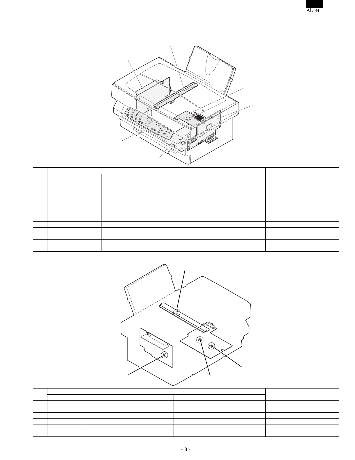
[5] EXTERNAL VIEW AND INTERNAL STRUCTURE
B. Internal parts
(1) Parts in each section
c. Optical section
<1> Scanner (reading) section
10)
11)
4) MHPS
8) SL SENSOR
2)
3)
2)
6) CCD SENSOR
5)
7)
9)
1)
4) MHPS
10) 8) SL SENSOR 7) 6) CCD SENS
11) 9) 5) 3)
Parts
No.
Code
1 Scanner lamp
Signal
name
Name Type Function/operation Active condition
Drives the scanner lamp. Maintains
control PWB
the lamp light quantity at a constant
level.
2 Scanner drive wire Transmits the scanner motor power
to the scanner unit.
3 Scanner motor Drives the scanner unit.
4 MHPS MHPS Scanner home
position sensor
Photo
transmission
sensor
Detects the scanner home position.
By this signal the image scanning
operation is controlled.
5 Lens Transfers the document image to
CCD.
6 CCD
SENSOR
CCD OUT CCD (Image)
sensor
CCD Scans the document images (photo
signals) and converts them into
electrical signals.
7 Scanner lamp Radiates light to the document to
allow the CCD to scan the document
images.
8 SL SENSOR PDA/PDK Scanner lamp light
quantity sensor
Photo diode Detects the scanner lamp light
quantity. This signal is inputted to the
scanner lamp control PWB to control
the scanner lamp drive voltage to
maintain a constant level of light
quantity.
9 No. 1 mirror Leads the document image to CCD.
10 No. 2 mirror Leads the document image to CCD.
11 No. 3 mirror Leads the document image to CCD.
OR
Note
HIGH (5V) when
the home position
is detected.
Digital signal (8Bit)
Analog signal
(0 ∼ 0.5V)
– 2 –
Page 5
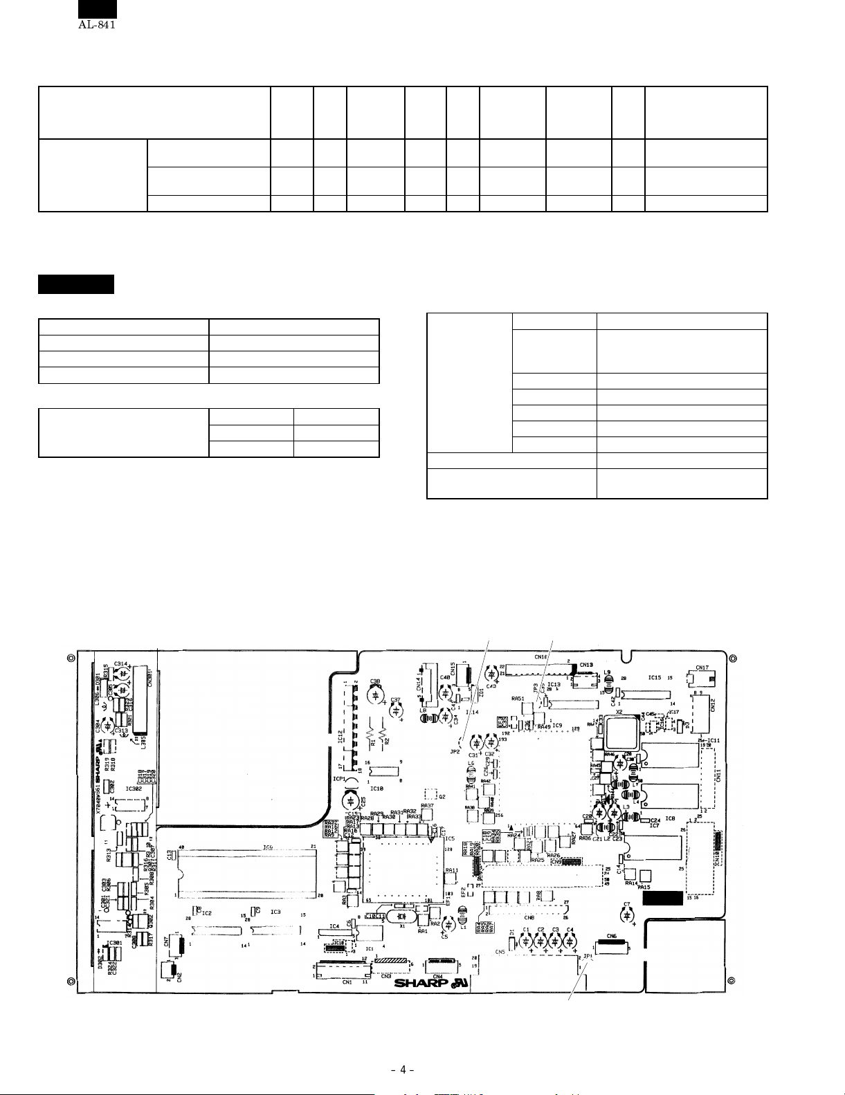
AL-841
C. Functional parts
(5) PWB
2)
1)
3)
4)
6)
5)
No.
Name Function/operation
1 Power PWB Outputs DC power. Drives the heater lamp. The voltage specification differs
2 Scanner lamp drive
Controls light quantity of the scanner lamp.
PWB
3 ICU PWB Converts print data set from the host and converts it into bit
image data and send to the MCU.
4 MCU (PCU) PWB Controls the image process section and the engine sect ion.
5 High voltage power
PWB
Outputs the high voltage for the image process section.
Controls the main motor.
6 Operation control PWB Displays the value information. Outputs the key operation
signal.
(11) Adjustment volume
Parts
MODEL Note
depending on the destination.
Allows connection with one
host computers. Printer models
only
1)
VR801
VR601
No.
Code Name Function/operation
Parts
1 VR1 Scanner lamp light quantity adjustment
Adjusts the scanner lamp light quantity.
VR802
volume
2 VR601 Output voltage adjustment vol ume Adjust the DC output voltage (+24V).
VR801 Main charger voltage adjustment volume Adjusts the main charger voltage.
VR802 Developing bias voltage adjustment
Adjusts the developing bias voltage.
volume
– 3 –
Note
Page 6
AL-841
[6] MACHINE OPERATION
ON
LINE
LAMP
ON OFF — OFF OFF OFF OFF ON
ON ON — OFF OFF OFF OFF ON
Scanner operation
Machine condition
Scanning cannot be
performed. (OFFLINE)
Scanning can be
performed. (ONLINE)
During scan/preview OFF ON — OFF OFF OFF OFF ON
READY
LAMP
[7] ADJUSTMENTS, SETTING
ADJ M9
Location value
∗
Range (MIN) 3.9 V
Range (MAX) 4.1 V
Standard value 4.0 V
Default 4.0 V
Program used
∗
Test command (Simulation) MODE Normal
Copy lamp light quantity adjustment
MAIN CODE 63
SUB CODE 1
3 GREEN
7
SEGMENT
LED
PRE-
JAM
HEAT
LAMP
LAMP
Enforcement time
∗
Enforcement
time
Cycle —
Condition Normal copy exposure is not
Necessary condition
∗
1) The scanner section must be clean.
TONER
CERTRIDGE
REPLACE-
MENT LAMP
S 004/Ua
001/
P 002
DRUM
CERTRIDGE
REPLACE-
MENT LAMP
JOB No Content
Copy
lamp
When replacing the scanner
(copy) lamp control PWB
When replacing the copy lamp
In case of E7 (05) trouble
In case of E7 (04) trouble
In case of E7 (12) trouble
In case of E7 (15) trouble
obtained.
NOTE
Job content
∗
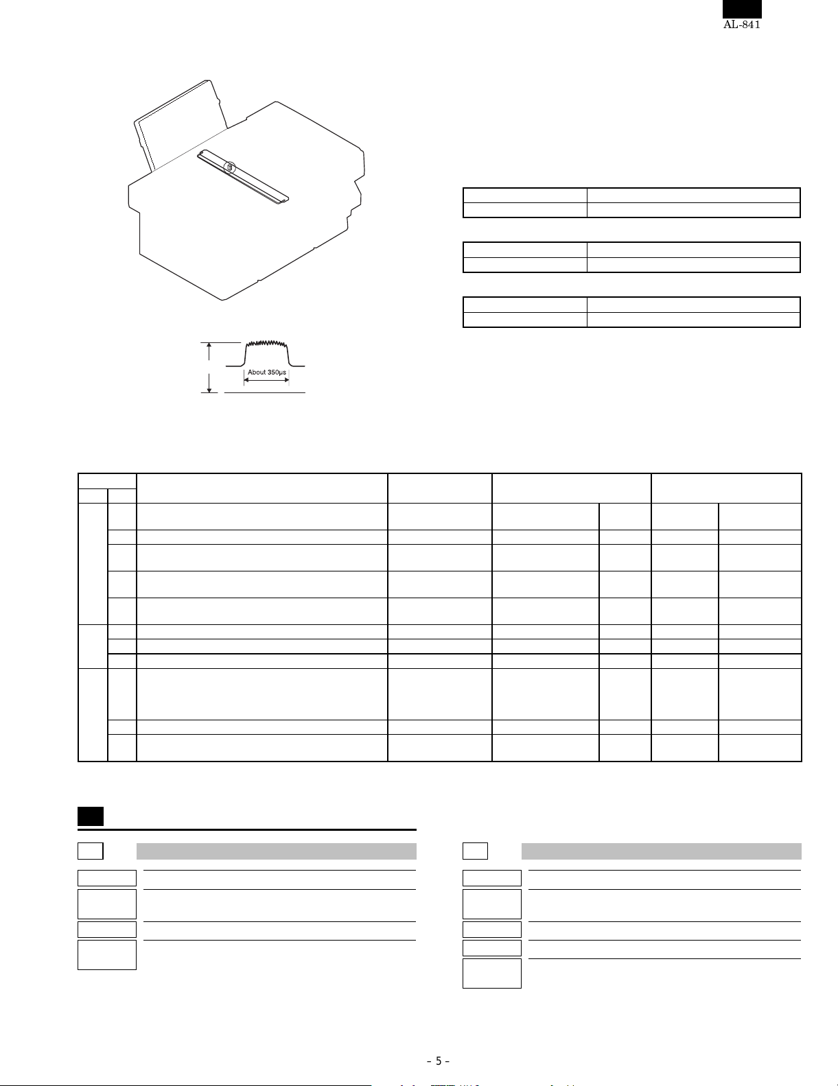
1) Put an oscilloscope between the check point JP2 (VIN) on the
MCU (PCU) PWB and GND.
At that time, trigger with the SH (JP3) signal to see the waveform
correctly.
JP2 (VIN) JP3 (SH)
2) Execute simulation 63-1. (The copy lamp lights up in the scanner
unit home position.)
JP1 (GND)
– 4 –
Page 7
AL-841
3) Turn and adjust the volume on the copy lamp drive PWB so that
the CCD output waveform max. value is 4.0 ± 0.1 V.
Trouble caused y improper operation
∗
1) E7 (05) trouble
2) E7 (04) trouble
3) E7 (12) trouble
4) E7 (15) trouble
5) Copy exposure cannot be adjusted.
6) Copy exposure abnormality
Preliminary work
∗
JOB No Content
S 004 Scanner (reading) section cleaning
After-work
∗
JOB No Content
ADJ M1 Copy exposure adjustm ent
Necessary tools
∗
Name Oscilloscope
Parts code/Price rank —
4.0±0.1V
[8] SIMULATION (Test Command) ⋅ USER PROGRAM
(2) Simulation list
Code
Main Sub
22 4 Used to check the number of total mis-feed (jam) in the
machine.
14 Used to check the ROM version. Others Software
17 Used to check the copy count number. Operation data output/
18 Used to check the print count number. Operation data output/
21 Used to check the frequency of use (scanning) of the
scanner (reading).
24 1 Used to clear the mis-feed (jam) counter in the machine. Data clear Counter
8 Used to clear the copy counter. Data clear Counter Copier
9 Used to clear the print counter. Data clear Counter Printer
26 2 Used to set Enable/Disable of the SPF and the FAX
functions. (When a trouble occurs in the SPF and the
FAX section, disable those functions to allow only copying
and scanning functions.
6 Used to set the specifications depending on destination. Setting Specifications Destination
7 Used to set the model (hardware) specifications. Setting PCU Specifications Operation mode
Function (Purpose) Purpose Section Item
Operation data output/
Check (Display/Print)
Check (Display/Print)
Check (Display/Print)
Operation data output/
Check (Display/Print)
Setting ADF/RADF/UDH/SPF Specifications
Optical (Image
scanning)
Trouble Misfeed
Counter Copier
Counter Printer
Counter Scanner
(3) Details of simulations
22
22-4
22-14
(Common)
Purpose Operation data output/Check (Display/Print)
Function
(Purpose)
Used to check the number of total mis-feed (jam) in
the machine.
Item Trouble Misfeed
Operation/
Procedure
The JAM counter value is displayed in 3 digits × 2
times.
Display example: 12345
012 → Blank → 345 → Blank → 012
0.7s 0.3s 0.7s 1.0s 0.7s
Purpose Others
Function
(Purpose)
Section PCU
Item Software
Operation/
Procedure
– 5 –
Used to check the ROM version.
The ROM version on the MCU PWB is displayed in 3
digits on the copy quantity display.
If any trouble occurs in the software operation, check
the version with this simulation.
Page 8
AL-841
22-17
Purpose Operation data output/Check (Display/Print)
Function
(Purpose)
Item Counter Copier
Operation/
Procedure
Used to check the copy count number.
The display format and the method are same as SIM
22-5 (Total printer counter display).
22-18
Purpose Operation data output/Check (Display/Print)
Function
(Purpose)
Item Counter Printer
Operation/
Procedure
Used to check the print count number.
The display format and the method are same as SIM
22-5 (Total printer counter display).
22-21
Purpose Operation data output/Check (Display/Print)
Function
(Purpose)
Section Optical (Image scanning)
Item Counter
Operation/
Procedure
Used to check the count of use (count of scanning)
of the scanner (reading) unit.
The display system and the method are the same as
those of SIM 22-5 (Total print counter display).
24
24-1
Purpose Data clear
Function
(Purpose)
Item Counter
24-8
Purpose Data clear
Function
(Purpose)
Item Counter Copier
24-9
Purpose Data clear
Function
(Purpose)
Item Counter Printer
Used to clear the mis-feed (jam) counter in the
machine.
Used to clear the copy counter.
Used to clear the print counter.
26
26-2
Purpose Setting
Function
(Purpose)
Section ADF/RADF/UDH/SPF
Item Specifications
Operation/
Procedure
Enter the desired code number corresponding to Enable/Disable
setup and press the Start button, and the setup will be effective.
26-6
Purpose Setting
Function
(Purpose)
Item Specifications
Operation/
Procedure
2) To change the set content, enter the code of your desired
setting and press the start button.
Destination code Detected paper size
Set
value
0
1 EX Japan
2 Japan
When the set value is changed, the paper size specification and the
fixed, enlarged, and reduced copy magnification ratios are changed.
26-7
Purpose Setting
Function
(Purpose)
Section PCU
Item Specifications Operation mode (Common)
Operation/
Procedure
Used to set Enable/Disable of the SPF and the FAX
functions. (When a trouble occurs in the SPF and the
FAX section, disable those functions to allow only
copying and scanning functions.
When this simulation is executed, the code of current
setup of ENABLE/DISABLE of SPF/FAX function is
displayed.
Set code number SPF/FAX function
0 Disable
1 Enable
Used to set the destination.
1) The currently set code of the destination is
displayed.
Destination
Used to set the model (hardware) specifications.
When this simulation is executed, the monitor lamp
corresponding to the model (hardware) is displayed.
Copy quantity display Copy speed (CPM)
66cpm
88cpm
Paper
type
Inch
series
AB
series
AB
series
Paper width
detector ON
11 5 8.5/
14 5 8.5
A4 (210 5
356 mm)
A4 (210 5
356 mm)
Paper width
detector OFF
8.5 5 5.5/
8.5 5 11
A5
B5
– 6 –
Page 9

AL-841
Page 10

S
AL-841
[9] ACTUAL WIRING CHART
Main
motor
PUS
HEATER
POWER-SW
123
AC
CN602
CN603
1 HL-L (100V) 12V 7 7 12V MMTO 7
HL-N (200V)
2
HL-L (200V)
3
4 HL-N (100V) HL 10 10 HL 12V 10
1 L-IN P-GND 14 14 P-GND PGND 14
2 L-OUT P-GND 15 15 P-GND MCON 15
3 N-IN P-GND 16 16 P-GND HLON 16
4 N-OUT 24V(DSW) 17 17 24V(DSW) TC/BIA
GND
AC
Power
supply
PWB
Developing cartridge
Developing roller
Photoconductor cartridge
Main charger roller
5V
GND
CN601
NC 1 1NC 24V(DSW) 1
D-GND 2 2 D-GND DGND 2
D-GND 3 3 D-GND DGND43
5V 4 4 5V
5V 5 5 5V MEN- 5
3.3V 6 6 3.3V MMT1 6
FW 8 8 FW PIN 8
PR 9 9 PR 3.3V 9
24VH 11 11 24VH FW 11
24VH 12 12 24VH
P-GND 13 13 P-GND PGND 13
24V(DSW)
18 18
24V(DSW)
19 19
Earth sheet
123
4
MA
MA-MBMB-
CN802 CN803
1
2
24V
PUS
CN805CN804
5V
High
voltage
24V(DSW)
24V(DSW)
FU
EARTH
DCBIASS
MC
PWB
PID sensor
24VH
PUS 18
PR 19
PWNSIN 20
12
17
Drum
Discharge brush
(Japan only)
Separation electrode
Copy roller
DRUM
EARTH
CB
TC
CN801
24VNC24VS
123
Temperature fuse
– 7 –
Page 11

D-GND
A-GND
CCDOUT
A-GND
A5V5V12V
123456789
CCD PWB
CN301
D-GNDf1D-GNDf2D-GND
SH-
D-GNDRSD-GNDSPD-GNDCPD-GNDNCD-GND
10111213141516171819202122
Laser
scanning
motor
12345
GND
PMD
24V
PMCLK
Laser
24V(DSW)
D-GND
VDATA
SAMP
SYNC-IN
1234567
CN602
LSU PWB
GND
APCSTT
PMCLK
PMD8
LSU unit
CN603
5VL 1 1 5VL
SYNC 2 2 SYNC
GND 3 3 GND
PE sensor
CN601
PEMP-IN
9
Laser beam
sensor
(Start position
detector PWB)
CN604
AL-841
OC
Open/close
SW
1
2
AN-GND
PSIZE-IN
CN17
CN5
1 24V(DSW)
2 DGND D-GND 1 1 D-GND
34DGND 5V1 2 25V1
5V
5 MEN- KIN2 4 4 KIN2
6 MMT1 KIN1 5 5 KIN1
7 MMTO OP-CLK 6 6 OP-CLK
8 PIN OP-LATCH 7 7
9 3.3V
10 12V STR1 9 9 STR1
11 FW STR2 10 10 STR2
24VH
12
13 PGND STR4 12 12 STR4
14 PGND
15 MCON
16 HLON
17 TC/BIAS
18 PUS
19 PR VFMOUT 1 1 VFMOUT
20 PWNSIN NC 2 2 NC
123456789
GND
A-GND
CCDOUT
A-GND
A5V5V12V
CN16
10111213141516171819202122
GNDf1GNDf2GND
SH-
GNDRSGNDSPGNDCPGNDNCGND
123456789
24V(DSW)
D-GND
VDATA
SAMP
SYNC-IN
APCSTT
PMCLK
CN12 CN14
PMD-
PEMP-IN
Scanner
motor
12345
OUT A
OUT B
OUT/A
OUT/B
24V-mir
CN1
KIN3 3 3 KIN3
OP-DATA OP-DATA
88
STR3 11 11 STR3
CN901
OP-LATCH
CN4
NC 3 3 NC
P-GND 4 4P-GND
NC 5 5 NC
MCU PWB
Operation panel
PWB
Fan motor
CN2
AN-GND
RTHIN5VTS IN
1
2
Thermistor
CN6
12345
12345
5V
TS IN
CN15
D-GND
P-GND
P-GND
GND
123
123
D-GNDNCP-GND5VMHPS IN
Toner detector sensor
CN7
MHPS IN5V5V
POUT IN
GD
123
GND
POD sensor
Scanner H.P sensor
5V5VPARAAD0
PARAAD1
PARAAD2
PARAAD3
PARAAD4
123456789
123456789
5V5VPARAAD0
PARAAD1
PARAAD2
PARAAD3
PARAAD4
CN8
PARAAD5
PARAAD6
PARAAD7
/REV
/INIT
/SLCTIN
/AUTOFD
/STB
/ACK
BUSYPE/FAULT
SLCT
/STB
/ACK
BUSYPE/FAULT
SLCT
GND
GND
1011121314151617181920212223242526
1011121314151617181920212223242526
PARAAD5
PARAAD6
PARAAD7
/REV
/INIT
/SLCTIN
/AUTOFD
CN203
GDI/USB PWB
– 8 –
Lamp
CN13
24V 1 1 24V
P-GND 2 2P-GND
ON/OFF 3 3 ON/OFF
NC 4 4 NC
GND
GND
/USB-EN
USB-ON
/1284-EN
3.3V
27
27
GND
GND
/USB-EN
USB-ON
/1284-EN
3.3V
CN1
Inverter PWB
Page 12

AL-841
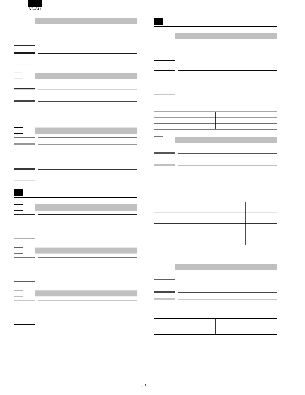
[10] CIRCUIT DIAGRAM AND PARTS LOCATION CHART
4
3
2
1
21
20
23
GND19GND
/DSTB
1
24
GND
GND22GND
GND
DATA 5
DATA 4
DATA 3
DATA 2
DATA 1
4
2
5
3
6
22J
22J
R214
R217
R216
1/1
E
D
5V1
C
IEEE1284 CON
CN202
R229
1.2kJ
R226
1.2kJ
R224
1.2kJ
R222
1.2kJ
R220
1.2kJ
R218
1.2kJ
R215
1.2kJ
R213
1.2kJ
D201
RB501-V40
B
(2-A3)
5V1
5V1
C242
0.1u
5V1
3A34A45A56A67A78A89
2
A1
A2
IC205
B5
B4
B3
B2
B1
C203
47u 10V
L203
SBO-02SAN
(2-A3)
3.3V
14
15
16
17
18
A
31
29
25
GND
DATA 6
7
22J
R219
B6
13
32
28
26
27
GND
GND
GND
GND
/ACK
DATA 8
DATA 7
8
9
10
2
1
2
1
2
1
2
1
22J
22J
R221
R223
C230
C229
C228
C227
C226
C225
C224
C222
C223
19
G
B8
B7
11
12
35
22J
R225
/INPRIM
SLCT
13
100p
100p
100p
100p
100p
100p
100p
100p
0.1u
/FAULT
/AUTOLF
14
D204
D203
D202
D201
22J
R228
74LS245
33
S GND
34
(NC)
(NC)
15
DAP202K
DAP202K
DAP202K
DAP202K
22J
16
3
3
3
3
S GND
17
VCC
F GND
36
/SLCTIN
VCC
18
R238
1.2kJ
R235
1.2kJ
R234
1.2kJ
R231
1.2kJ
R232
5V1
4
2
1A1
1A2
IC206
1Y2
1Y1
18
16
3.3kJ
R239
5V1
SHIELD
5V1
F.G
100J 1/2W
R201
2
3
1
D209
DAP202K
D206
DAP202K
2
3
1
D205
DAP202K
2
3
1
22J
22J
22J
22J
R236
R233
R237
560p
C235
C234
33p
C233
33p
C232
1000p
(2-A2)
(2-A2)
(2-A2)
(2-A2)
/SLCTIN
/STB
/AUTOFD
/INIT
C231
0.1u
19
8
6
13
15
17
11
1G12G
2A1
2A2
2A3
1A3
2A4
1A4
2Y4
2Y272Y3
2Y1
1Y4
1Y3
9
12
14
74LS244
5
3
22J
R240
R241
16
14
18
1Y1
1Y2
1Y3
IC207
1A3
1A2
1A1
4
2
6
5V1
5V1
2
3
1
D208
DAP202K
2
3
1
D207
DAP202K
22J
22J
22J
22J
R243
R242
R244
100p
C241
100p
C240
100p
C239
100p
C238
100p
C237
(2-A4)
(2-A2)
(2-A2)
(2-A3)
(2-A3)
(2-A1)
(2-A1)
(2-A1)
(2-A1)
5
3
7
9
12
2Y1
2Y2
2Y3
2Y4
1Y4
2A4
2A3
2A2
2A1
2G
1A4
8
13
11
74LS244
1G
17
15
19
1
0.1u
C236
(2-A1)
/FAULT
/ACK
BUSY
PE
SLCT
(2-A3)
PARAAD7
(2-A3)
PARAAD6
PARAAD5
PARAAD4
(2-A2)
PARAAD3
(2-A2)
PARAAD2
PARAAD1
PARAAD0
USB-ON
/USB-EN
E
D
C
(2-A4)
B
30
GND
BUSY
11PE12
1
DIR
A
GDI PWB
PARAAD0
PARAAD1
PARAAD2
PARAAD3
PARAAD4
PARAAD6
PARAAD7
/REV
/INIT
/SLCTIN
/AUTOFD
/STB
/ACK
PARAAD5
123456789
CN203
4
BUSYPE/FAULT
1011121314151617181920212223242526
3
SLCT
/1284-EN
/USB-EN
USB-ON
27
27FMN-STK
2
1
– 9 –
Page 13

GDI PWB (PARTS LAYOUT)
[PARTS SURFACE]
AL-841
[SOLDER SURFACE]
123456789
5V5VPARAAD0
PARAAD1
PARAAD2
CN203
PARAAD3
1011121314151617181920212223242526
PARAAD4
PARAAD5
PARAAD6
PARAAD7
/REV
/INIT
/SLCTIN
/AUTOFD
/STB
/ACK
BUSYPE/FAULT
SLCT
GND
GND
GND
/USB-EN
USB-ON
/1284-EN
27
3.3V
– 10 –
Page 14

AL-841
Page 15

PARTS GUIDE
DIGITAL COPI ER
MODEL AL-841
CONTENTS
(Exteriors)
(Operation Panel)
(Packing Material & Accessories)
(Frame Section)
MCU (MCU PWB Unit)
(Upper Frame Section)
1
(Lower Frame Section-1)
2(Lower Frame-2)
(Fusing Unit)
(Scanner Unit)
AL-841 AL-800/840 AL-800/840
(Operation Panel PWB Unit)
GDI (GDI PWB Unit)
1 (Carriage 1 Unit)
&
(Power Supply PWB Unit)
(High Voltage PWB Unit)
(Index)
The AL-841 Parts Guide describes only the different parts from the AL-800/840. Please use this Parts
Guide together that of the AL-800/840.
Page 16

DEFINITION
The definition of each Rank is as follows and also noted in the list
A :Parts necessary to be stocked as High usage parts.
B :Parts necessary to be stocked as Standard usage parts.
C :Low usage parts.
D : Parts necessary for refurbish.
E :Unit parts recommended to be stocked for efficient after sales service.
Please note that the lead time for the said parts may be longer than normal parts.
S : Consumable parts.
Please note that the following parts used in Copier under the same description are classified into A or B Rank depending
upon the place used.
Example: Gear made of Metal, Sprocket, Bearing, Belt made of Rubber, Spring clutch mechanism.
A Rank : The parts which may be with the revolution or loading.
B Rank : Parts similar to A Rank parts, but are not included in Rank A.
Because parts marked with “ ” is indispensable for the machine safety maintenance and operation, it must be replaced with
the parts specific to the product specification.
Other than this Parts Guide, please refer to documents Service Manual (including Circuit Diagram) of this model.
Please use the 13 digit code described in the right hand corner of front cover of the document, when you place an order.
For U.S. only-Use order codes provided in advertising literature. Do not order from parts department.
1 (Exteriors)
NO. PARTS CODE
1
2 AN EQ N C
3 AF DS N C
4 AQ EQ N C
6 AU EZ N C
8 AG DX N C
9 AH DX N C
10 AH DX N C
11
12 AS EQ N C
14 AT EZ N C
15 AG DX N C
16
22 AE DJ N C
23 AU FG N C
24
26
27
29 AC DJ N C
501
502 AU EZ N E
PRICE RANK
Ex. Ja.
AK DX N C
BG GT N E
BG GT N E
AH DX N C
AS EZ C
AG DX N C
AG DX N C
AG DX N C
AG DS N C
AU EZ N E
AT EZ N E
NEW
MARK
PART
RANK
PU EX tray PU
PU tray PU
Paper guide
Rear cabinet
Right cabinet
Delivery tray
Delivery extension lower
Left cabinet lower
Operation panel unit (Japan)
Operation panel unit (USA)
Front cabinet
Left cabinet
OC switch acutuator OCRight cabinet lower
OC hinge OC
OC cover OC
OC mat OC
Operation label (Japan)
Operation label (USA)
Platen label (Japan)
Platen label (USA)
Tray label (Japan Only)
Paper feed unit (Japan)
Paper feed unit (USA)
Oc cover unit OC
DESCRIPTION
-
-
-
– 1 –
Page 17

2 (Operation Panel)
NO. PARTS CODE
1
2 AR EQ C
5
8
9 AK EB N C
10
11
(Unit)
901
PRICE RANK
Ex. Ja.
BV RB N E
AT EZ N C
AV FG C
AV FG N C
AV FG N C
AL EB N C
AF DS C
BG GT N E
BG GT N E
NEW
MARK
PART
RANK
Operation PWB unit
Operation FFC
Operation panel cabinet (Japan)
Operation panel cabinet (USA)
Operation panel (Japan)
Operation panel (USA)
Operation key R
Operation key L
Cable cover sheet
Operation panel unit (Japan)
Operation panel unit (USA)
3 (Frame Section)
NO. PARTS CODE
4
PRICE RANK
Ex. Ja.
AG DS C
NEW
MARK
PART
RANK
Release lever
4 (Upper Frame Section)
NO. PARTS CODE
14
30 BQ LP N E
PRICE RANK
Ex. Ja.
AB DJ C
NEW
MARK
PART
RANK
DV press spring DV
Toner sensor PWB unit
5 1(Lower Frame Section-1)
NO. PARTS CODE
15
39 BB FX C
47 AB DJ C
52
PRICE RANK
Ex. Ja.
AG DX N C
AD DJ C
NEW
MARK
PART
RANK
Tray lock lever
Lower frame
Release lever spring
Electricity plate (Japan Only)
DESCRIPTION
FFC
- R
- L
- -
DESCRIPTION
- -
DESCRIPTION
- -
DESCRIPTION
R
6 2(Lower Frame-2)
NO. PARTS CODE
1
7
9 AP EQ C
13 AG DX N C
14
15
PRICE RANK
Ex. Ja.
CA TV N E
CA TV N E
BK HG E
BL HL N E
BL HL N E
BN HZ E
BP LP N E
NEW
MARK
7 (Fusing Unit)
NO. PARTS CODE
17
26 AV FG C
PRICE RANK
Ex. Ja.
BG GT N E
NEW
MARK
8 (Scanner Unit)
NO. PARTS CODE
1
5 BE GN N E
8 AA DJ C
13 AN EG N B
26 AH DX C
27
28 BB FX B
29
33 AC DJ C
42 BT MW N E
51 AF DS N C
54
PRICE RANK
Ex. Ja.
AK DX C
AX FG C
AK DX C
AX FG B
NEW
MARK
PART
RANK
MCU PWB unit (Japan) MCU
MCU PWB unit (USA) MCU
High voltage PWB unit (Japan)
High voltage PWB unit (USA)
Bottom plate
ICU FFC ICU-FFC
GDI PWB unit GDI
Power supply PWB unit (100V Japan)
Power supply PWB unit (120V USA)
PART
RANK
POD PWB unit P-OUT
FU roller FU
PART
RANK
Dark box
Carriage 1 unit
Table glass rubber
Micro switch unit
Frame R
Mein frame
Mirror motor
Motor fixing plate
Belt tension spring
Lens base unit
Myler CCD
Table glass
DESCRIPTION
DESCRIPTION
DESCRIPTION
1
- R
-
- - -
- -
-
-
– 2 –
Page 18

9 1 (Carriage 1 Unit)
NO. PARTS CODE
1
4
6 AH DX N C
8 AF DS C
11
14
15
16
17 AD DJ N C
18 AA DD C
19 AA DD C
20 AA DD C
(Unit)
901
PRICE RANK
Ex. Ja.
AC DJ N C
AG DX N C
AD DJ N C
AD DJ N C
AC DJ N C
BA FX N E
BE GN N E
NEW
MARK
PART
RANK
Lamp cover L
Inverter harness
Lamp base
Carriage 1
Carriage 1 base F
Carriage 1 base R
Lamp cover R
Lamp PWB unit
Sub reflector
Screw (2×8)
Screw (3×6)
Screw (3×6)
Carriage 1 unit
11 & (Packing Material & Accessories)
NO. PARTS CODE
4
5 AE DJ N D
6 AM EG N D
7
12
104
110 AG DX D
111 AC DJ D
113 AB DJ D
PRICE RANK
Ex. Ja.
AM EG N D
AS EZ N D
AS EZ N D
AM EG N C
AM EG N C
AW FG N D
AW ZZ N D
AE DJ N D
AE DJ N D
AC DJ N D
AF DS N D
NEW
MARK
PART
RANK
Packing add upper
Body vinyl
Packing add lower
Packing case (Japan)
Packing case (USA)
CDROM (Japan) CDROM
CDROM (USA) CDROM
Operation manual (USA)
Operation manual (Japan)
eTypist Operation manual (Japan) eTypist
Up grade guidance (Japan)
Sample card (Japan)
Postcard (Japan)
Drum sheet
Slip sheet (USA)
Label (USA)
DESCRIPTION
- L
- -
1
1 F
1 R
- R
1
DESCRIPTION
-
-
1 (Exteriors)
14
26
11
10
27
4
29
3
15
23
22
22
2
1
501
502
24
12
8
16
9
6
PRPN0030
– 3 –
Page 19

2 (Operation Panel) 3 (Frame Section)
10
2
1
9
8
11
5
4 (Upper Frame Section) 5 1(Lower Frame Section-1)
39
15
30
14
47
47
52
4
6 2(Lower Freme-2) 7 (Fusing Unit)
14
C
1
B
13
A
9
7
B
A
17
15
C
26
PRPN0031
– 4 –
Page 20

8 (Scanner Unit) 9 1 (Carriage 1 Unit)
18
54
9
2
9
18
1
1
6
17
16
15
20
4
5
51
13
8
26
33
29
8
8
8
27
28
42
8
8
11 & (Packing Material & Accessories)
11
19
14
8
12
5
4
6
7
PRPN0032
– 5 –
Page 21

12 MCU (MCU PWB Unit)
NO. PARTS CODE
1
2 AA DD C
3 AB DJ C
4 AB DD C
5 AE DJ C
6 AD DJ C
7 AB DJ C
8 AC DJ C
9 AE DS C
10 AF DS C
11 AG DS C
12 AD DJ C
13 AE DJ C
14 AD DJ C
15 AP EQ B
16 AG DS B
17 AC DJ C
18 AA DD B
19
20 AB DD B
21
22 AA DD C
23 AA DD C
24 AA DD C
25 AA DD C
26 AA DD C
27 AB DD C
28 AB DD C
29 AA DD C
30 AC DD C
31
32
33 AA DD C
34 AB DD C
35 AA DD C
36 AA DD C
37 AA DD C
38 AB DD B
39 AC DD B
40 AC DD B
41 AB DJ B
42 AB DJ B
43 AB DJ B
44 BE GN B
45
46
47
48
49
50
51
52
53
54
55
56
57
58
59
60
61
62
PRICE RANK
Ex. Ja.
AD DJ C
AB DD B
AB DD B
AB DD B
AB DD B
AA DD C
AA DD C
AA DD C
AA DD C
AA DD C
AA DD C
AA DD C
AA DD C
AY FQ B
AU EZ B
AC DJ B
AQ EQ B
AY FQ B
AG DS B
AF DS B
AT EZ B
AD DJ B
AF DX B
AQ EQ B
AF DS B
AF DJ B
AH DX B
AE DS B
AN EG B
BA FX B
AF DS B
NEW
MARK
PART
RANK
Connector (2pin) [CN2]
Connector (3pin) [CN15,17]
Connector (5pin) [CN4,6]
Connector (2pin) [CN17]
Connector (5pin) [CN14]
Connector (9pin) [CN12]
Connector (4pin) [CN13]
Connector (12pin) [CN1]
Connector (22pin) [CN16]
Connector (27pin) [CN18]
Connector (20pin) [CN5]
IC socket (40pin) [IC6] IC
Coil (NFM839R02C470R101) [EF1∼EF3]
Coil (SBO-02SAN) [L1∼9]
Crystal (11.85737433MHz) [X2]
Crystal (19.99370079MHz) [X1]
Bead filter (ZE221) [L101]
Block resistor (10Ω×4) [RA5∼8,21,24,45,46]
Block resistor (10KΩ×4 1/32W ±5%)
Block resistor (10KΩ×4 1/32W ±5%)
Block resistor (22Ω×4) [RA49,51]
Block resistor (47Ω×4 1/32W ±5%) [RA10,13,17,23,25∼27]
Block resistor (47Ω×4 1/32W ±5%) [RA30∼36,40∼42]
Capacitor (50WV 10pF) [C137,138]
Capacitor (50WV 100pF)
[C139∼141,146,148,160,161,194∼199,201,211,213,214,239]
Capacitor (50WV 12pF) [C228]
Capacitor (50WV 33pF) [C229]
Capacitor (16WV 22µF) [C3∼5]
Capacitor (25WV 47µF) [C38]
Capacitor (50WV 47µF) [C25]
Capacitor (35WV 10µF) [C21,22,28,31,32,34,37,40,43]
Capacitor (35WV 22µF) [C1,2,7]
Capacitor (25WV 0.10µF)
Capacitor (25WV 0.10µF)
Capacitor (25WV 0.10µF)
Capacitor (25WV 0.10µF)
Capacitor (50WV 1000pF)
Capacitor (50WV 1000pF)
[C113∼115,117∼119,124∼130,133,144,152,154,158,159,162]
Capacitor (50WV 1000pF)
Capacitor (50WV 1000pF)
Capacitor (50WV 2200pF) [C225,240,241,255]
Capacitor (50WV 470pF) [C220,250,276∼280]
Capacitor (50WV 4700pF) [C149]
Capacitor (25WV 0.10µF) [C120,121,134,221,244,247,265,273]
Capacitor (50WV 0.022µF) [C131,132,136,231,232,245]
Diode (DAN202K) [D123]
Diode (DAN217) [D113,114]
Diode (DA204K)
Diode (IN4005E) [D2]
Diode (1SS355) [D1,3]
Zener diode (RLZ2.0A) [ZD1]
IC (HG73C025FD) [IC9] IC
CPU (H8S/2350FP) [IC5] CPU
IC (LH50506N) [IC109] IC
IC (LM358PS) [IC104] IC
IC (LM7121) [IC107] IC
IC (MX27C2048D) [IC6] IC
IC (M24C02WBN6) [IC1] IC
IC (M51953BL) [IC 4]IC
IC (M66236FP) [IC101]IC
IC (NJM2903M) [IC102] IC
IC (NJM3414M) [IC106] IC
IC (SLA7027MU) [IC12] IC
IC (TC7W66FU) [IC14] IC
IC (TC74HC08F1) [IC108] IC
IC (TC74HC14FN) [IC103] IC
IC (TD62003AF) [IC10] IC
IC (W24257A12J) [IC2,3,13,15] IC
64MDRAM (16163CLT-6) [IC7,8,11] 64MDRAM
IC protector (ICPN38) [ICP1] IC
[C30,33,36,39,41,42,104,109,122,123,135,142]
[C151,153,204,209,210,212,215,216,222,224,226]
[C227,230,233∼235,238,242,246,254,262,263,271,272]
[C11,12,16,18,26,35,103,105∼108,110,111]
[C165∼168,180,182,202,206,208,217,218,223,243,249]
[C251,252,256,258∼261,264,266∼270,274,275]
DESCRIPTION
[RA1∼4,9,11,12,14∼16]
[RA18,19,22,28,29,37,39,43,44,47]
[C6,8∼10,13∼15,17,19,20,23,24,27,29]
[D101∼103,111,112,115∼122,124∼127]
– 6 –
Page 22

12 MCU (MCU PWB Unit)
NO. PARTS CODE
63
64 AA DD C
65 AA DD C
66
67
68 AA DD C
69 AA DD C
70 AA DD C
71 AA DD C
72 AA DD C
73 AA DD C
74 AA DD C
75 AA DD C
76 AA DD C
77 AA DD C
78 AA DD C
79 AA DD C
80 AA DD C
81 AA DD C
82 AA DD C
83 AA DD C
84 AA DD C
85 AA DD C
86 AB DD C
87 AA DD C
88 AA DD C
89 AA DD C
90 AA DD C
91 AA DD C
92 AB DD B
(Unit)
901
PRICE RANK
Ex. Ja.
AA DD C
AA DD C
AA DD C
AA DD C
AA DD C
CA TV N E
CA TV N E
NEW
MARK
PART
RANK
Resistor (1/16W 0Ω±5%) [R123,129,141,175,209,250]
Resistor (1/16W 10Ω±5%)
[R103∼105,143,147,154,159,160,163,189,191,207,218,229]
Resistor (1/16W 100Ω±5%) [R134,196,230]
Resistor (1/16W 1.0KΩ±5%)
Resistor (1/16W 1.0KΩ±5%) [R203,231,237∼239,242]
Resistor (1/16W 10KΩ±5%)
Resistor (1/16W 10KΩ±5%) [R225,243,251∼258]
Resistor (1/16W 1.2KΩ±5%) [R200]
Resistor (1/16W 1.6KΩ±5%) [R111,112,119,201]
Resistor (1/16W 20KΩ±5%)
Resistor (1/16W 2.0MΩ±5%) [R195,221]
Resistor (1/16W 22Ω±5%) [R199]
Resistor (1/16W 2.4KΩ±5%) [R219,220]
Resistor (1/16W 270Ω±5%) [R234]
Resistor (1/16W 330Ω±5%) [R139]
Resistor (1/16W 33KΩ±5%) [R115]
Resistor (1/16W 390Ω±5%) [R226]
Resistor (1/16W 47Ω±5%) [R174]
Resistor (1/16W 47KΩ±5%) [R188,205,227]
Resistor (1/16W 680Ω±5%) [R232]
Resistor (1/16W 75Ω±5%) [R213]
Resistor (1/16W 750Ω±5%) [R212]
Resistor (1/16W 7.5KΩ±5%) [R202]
Resistor (1/16W 910Ω±5%) [R133]
Resistor (1/16W 9.1KΩ±5%) [R114]
Resistor (2W 1.0Ω±5%) [R1,2]
Resistor (1/8W 180Ω±5%) [R126]
Resistor (1/8W 4.3KΩ±5%) [R125]
Resistor (1/8W 4.7KΩ±5%) [R192]
Resistor (1/16W 10KΩ±1%) [R208,216]
Resistor (1/16W 16.5KΩ±1%) [R206]
Transistor (2SA1036KQRC) [Q101]
MCU PWB unit (Japan) MCU
MCU PWB unit (USA) MCU
[R109,113,117,118,120,124,131,142,148,151,157,161]
[R106,107,127,128,149,152,158,162,193,204,222,224]
DESCRIPTION
[R108,132,140,144∼146,211,240,241]
13 (Operation Panel PWB Unit)
NO. PARTS CODE
1
2 AC DJ N B
3 AA DD C
4 AB DD C
5 AA DD C
6 AA DD B
7 AN EQ B
8
9
10
11
12 AA DD C
13 AA DD C
14 AA DD C
15 AA DD C
16 AA DD C
17 AD DJ B
(Unit)
901
PRICE RANK
Ex. Ja.
AC DJ C
AP EQ B
AC DJ B
AC DJ B
AC DJ B
AA DD C
BV RB N E
NEW
MARK
PART
RANK
Connector (12pin) [CN901]
Tact swtch (SKQNAB010)
Capacitor (50WV 200PF) [C904∼906]
Capacitor (16WV 47µF) [C902]
Capacitor (50WV 0.022µF) [C901,903]
Diode (DSS133) [D901∼904]
IC (LC7935) [IC901] IC
LED (CST338G-25) [LEDM] LED
LED (MPG3864K)
LED (MPG3864K) [3RE,EXD,EXN,EXL,AE,ME,PE] LED
LED (MVR3864K) [JPL,DPL,TPL] LED
Resistor (1/8W 0Ω±5%) [J900,901]
Resistor (1/10W 1.0KΩ±5%) [R935]
Resistor (1/10W 10KΩ±5%) [R938,962]
Resistor (1/10W 120Ω±5%) [R902∼918]
Resistor (1/10W 150Ω±5%) [R939∼941]
Resistor (1/10W 1.5KΩ±5%) [R936,937]
Digital transistor (DTB113ZK) [Q901∼903]
Operation PWB unit
DESCRIPTION
[OLK,PSW,CLK,1UPK,10UPK,MAGK,ZUPK,
[PML,ONLL,RPL,ZPL,2ENR,1ENR,NOR,1RE,
ZDWK,CRSK,EXUDK,EXMODK]
2RE,3RE,EXD,EXN,EXL,AE,ME,PE] LED
– 7 –
Page 23

14 GDI (GDI PWB Unit)
NO. PARTS CODE
1
2 AF DS C
3 AD DJ C
4 AA DD C
5 AA DD C
6 AA DD C
7 AB DD C
8 AA DD C
9 AA DD C
10 AA DD C
11 AB DD B
12 AH DX B
13
14
15 AA DD C
16 AA DD C
17 AA DD C
18 AA DD C
19 AA DD C
(Unit)
901
PRICE RANK
Ex. Ja.
AH DX C
AF EB B
AA DD C
BL HL N E
NEW
MARK
PART
RANK
Connector (36pin) [CN202]
Connector (27pin) [CN203]
Coil (SBO-02SAN) [L201,203]
Capacitor (50WV 100PF)
Capacitor (50WV 33pF) [C233,234]
Capacitor (50WV 560PF) [C235]
Capacitor (10WV 47µF) [C203]
Capacitor (25WV 4.7uF) [C201]
Capacitor (25WV 0.10µF) [C206,223,231,236,242]
Capacitor (50WV 1000PF) [C232]
Diode (DAP202K) [D201∼209]
IC (74LS244NS1) [IC206,207] IC
IC (74LS245NS1) [IC205] IC
Resistor (1/2W 100Ω±5%) [R201]
Resistor (1/10W 1.0KΩ±5%) [R227,230]
Resistor (1/10W 10KΩ±5%) [R247∼250]
Resistor (1/10W 1.2KΩ±5%)
Resistor (1/10W 22Ω±5%)
Resistor (1/10W 3.3KΩ±5%) [R239]
GDI PWB unit GDI
15 (Power Supply PWB Unit)
NO. PARTS CODE
(Unit)
901
PRICE RANK
Ex. Ja.
BN HZ E
BP LP N E
NEW
MARK
PART
RANK
Power supply PWB unit (100V Japan)
Power supply PWB unit (120V USA)
DESCRIPTION
[C222,224∼230,237∼241]
[R213,215,218,220,222,224,226,229,231,234,235,238]
[R214,216,217,219,221,223,225,228,232,236,237,240∼244]
DESCRIPTION
16 (High Voltage PWB Unit)
NO. PARTS CODE
1
(Unit)
901
PRICE RANK
Ex. Ja.
AR EQ B
BK HG E
BL HL N E
NEW
MARK
PART
RANK
IC (A2918SWH) IC
High voltage PWB unit (Japan)
High voltage PWB unit (USA)
DESCRIPTION
– 8 –
Page 24

■ (Index)
PARTS CODE
JAPAN ONLY
ORDER CODE
PRICE R.
NO.
Ex.
1- 12 AS EQ N C
1-502 AU EZ N E
8- 42 BT MW N E
11- 12 AM EG N C
11- 12 AM EG N C
8- 29 AK DX C
1- 11 BG GT N E
2-901 BG GT N E
1- 11 BG GT N E
2-901 BG GT N E
6- 7 BL HL N E
16-901 BL HL N E
6- 7 BK HG E
16-901 BK HG E
4- 30 BQ LP N E
7- 17 BG GT N E
6- 15 BN HZ E
15-901 BN HZ E
9- 16 BA FX N E
6- 15 BP LP N E
15-901 BP LP N E
6- 14 BL HL N E
14-901 BL HL N E
2- 1 BV RB N E
13-901 BV RB N E
6- 1 CA TV N E
12-901 CA TV N E
6- 1 CA TV N E
12-901 CA TV N E
8- 5 BE GN N E
9-901 BE GN N E
1-501 AT EZ N E
1-501 AU EZ N E
8- 13 AN EG N B
2- 2 AR EQ C
9- 4 AG DX N C
6- 13 AG DX N C
2- 5 AT EZ N C
2- 5 AV FG C
1- 6 AU EZ N C
1- 14 AT EZ N C
1- 4 AQ EQ N C
1- 16 AH DX N C
1- 10 AH DX N C
1- 23 AU FG N C
2- 8 AV FG N C
2- 8 AV FG N C
2- 9 AK EB N C
2- 10 AL EB N C
9- 11 AD DJ N C
9- 14 AD DJ N C
9- 6 AH DX N C
8- 27 AX FG C
5- 39 BB FX C
8- 26 AH DX C
6- 9 AP EQ C
1- 1 AK DX N C
1- 2 AN EQ N C
1- 8 AG DX N C
1- 9 AH DX N C
1- 22 AE DJ N C
5- 15 AG DX N C
3- 4 AG DS C
1- 15 AG DX N C
9- 8 AF DS C
4- 14 AB DJ C
5- 47 AB DJ C
8- 33 AC DJ C
7- 26 AV FG C
8- 1 AK DX C
Ja.
NEW P/R
PARTS CODE
JAPAN ONLY
ORDER CODE
PRICE R.
NO.
9- 1 AC DJ N C
9- 15 AC DJ N C
1- 3 AF DS N C
8- 54 AX FG B
8- 8 AA DJ C
9- 17 AD DJ N C
1- 24 AS EZ C
2- 11 AF DS C
11-110 AG DX D
8- 51 AF DS N C
12- 1 AD DJ C
12- 2 AA DD C
12- 3 AB DJ C
12- 4 AB DD C
12- 5 AE DJ C
12- 6 AD DJ C
14- 1 AH DX C
12- 7 AB DJ C
12- 8 AC DJ C
13- 1 AC DJ C
12- 9 AE DS C
12- 10 AF DS C
14- 2 AF DS C
12- 11 AG DS C
5- 52 AD DJ C
12- 12 AD DJ C
13- 2 AC DJ N B
12- 13 AE DJ C
12- 14 AD DJ C
14- 3 AD DJ C
12- 15 AP EQ B
12- 16 AG DS B
12- 17 AC DJ C
8- 28 BB FX B
12- 18 AA DD B
12- 19 AB DD B
12- 20 AB DD B
12- 21 AB DD B
11- 4 AM EG N D
11- 6 AM EG N D
11- 7 AS EZ N D
11- 7 AS EZ N D
11- 5 AE DJ N D
11-111 AC DJ D
11-104 AE DJ N D
11-104 AE DJ N D
11-104 AC DJ N D
11-104 AF DS N D
11-104 AW FG N D
11-104 AW ZZ N D
11-113 AB DJ D
1- 27 AG DS N C
1- 26 AG DX N C
1- 26 AG DX N C
1- 27 AG DX N C
1- 29 AC DJ N C
12- 22 AA DD C
12- 23 AA DD C
12- 24 AA DD C
12- 25 AA DD C
14- 4 AA DD C
13- 3 AA DD C
14- 5 AA DD C
14- 6 AA DD C
14- 7 AB DD C
14- 8 AA DD C
12- 29 AA DD C
12- 30 AC DD C
12- 26 AA DD C
12- 27 AB DD C
12- 28 AB DD C
13- 4 AB DD C
12- 31 AA DD C
12- 32 AA DD C
12- 33 AA DD C
Ex.
Ja.
NEW P/R
– 9 –
Page 25

PARTS CODE
JAPAN ONLY
ORDER CODE
PRICE R.
NO.
12- 34 AB DD C
12- 35 AA DD C
12- 36 AA DD C
14- 9 AA DD C
14- 10 AA DD C
12- 37 AA DD C
13- 5 AA DD C
12- 42 AB DJ B
12- 40 AC DD B
12- 38 AB DD B
12- 39 AC DD B
14- 11 AB DD B
13- 6 AA DD B
12- 41 AB DJ B
12- 43 AB DJ B
12- 61 BA FX B
14- 12 AH DX B
14- 13 AF EB B
16- 1 AR EQ B
12- 45 AY FQ B
12- 44 BE GN B
13- 7 AN EQ B
12- 46 AU EZ B
12- 47 AC DJ B
12- 48 AQ EQ B
12- 50 AG DS B
12- 51 AF DS B
12- 52 AT EZ B
12- 49 AY FQ B
12- 53 AD DJ B
12- 54 AF DX B
12- 55 AQ EQ B
12- 57 AF DJ B
12- 58 AH DX B
12- 56 AF DS B
12- 59 AE DS B
12- 60 AN EG B
13- 8 AP EQ B
13- 9 AC DJ B
13- 10 AC DJ B
12- 62 AF DS B
14- 14 AA DD C
12- 63 AA DD C
12- 64 AA DD C
12- 65 AA DD C
12- 66 AA DD C
12- 67 AA DD C
12- 68 AA DD C
12- 69 AA DD C
12- 70 AA DD C
12- 71 AA DD C
12- 72 AA DD C
12- 73 AA DD C
12- 74 AA DD C
12- 75 AA DD C
12- 76 AA DD C
12- 77 AA DD C
12- 78 AA DD C
12- 79 AA DD C
12- 80 AA DD C
12- 81 AA DD C
12- 82 AA DD C
12- 83 AA DD C
12- 84 AA DD C
12- 85 AA DD C
12- 86 AB DD C
13- 11 AA DD C
12- 87 AA DD C
12- 88 AA DD C
12- 89 AA DD C
13- 12 AA DD C
14- 15 AA DD C
13- 13 AA DD C
14- 16 AA DD C
13- 14 AA DD C
14- 17 AA DD C
13- 15 AA DD C
13- 16 AA DD C
14- 18 AA DD C
14- 19 AA DD C
12- 90 AA DD C
Ex.
Ja.
NEW P/R
PARTS CODE
JAPAN ONLY
ORDER CODE
PRICE R.
NO.
12- 91 AA DD C
12- 92 AB DD B
13- 17 AD DJ B
9- 18 AA DD C
9- 19 AA DD C
9- 20 AA DD C
Ex.
Ja.
NEW P/R
– 10 –
Page 26

AL-841
Page 27

CAUTION FOR BATTERY REPLACEMENT
(Danish) ADVARSEL !
Lithiumbatteri – Eksplosionsfare ved fejlagtig håndtering.
Udskiftning må kun ske med batteri
af samme fabrikat og type.
Levér det brugte batteri tilbage til leverandoren.
(English) Caution !
Danger of explosion if battery is incorrectly replaced.
Replace only with the same or equivalent type
recommended by the manufacturer.
Dispose of used batteries according to manufacturer’s instructions.
(Finnish) VAROITUS
Paristo voi räjähtää, jos se on virheellisesti asennettu.
Vaihda paristo ainoastaan laitevalmistajan suosittelemaan
tyyppiin. Hävitä käytetty paristo valmistajan ohjeiden
mukaisesti.
(French) ATTENTION
Il y a danger d’explosion s’ il y a remplacement incorrect
de la batterie. Remplacer uniquement avec une batterie du
même type ou d’un type équivalent recommandé par
le constructeur.
Mettre au rebut les batteries usagées conformément aux
instructions du fabricant.
(Swedish) VARNING
Explosionsfara vid felaktigt batteribyte.
Använd samma batterityp eller en ekvivalent
typ som rekommenderas av apparattillverkaren.
Kassera använt batteri enligt fabrikantens
instruktion.
AL-841
Page 28

AL-841
All rights reserved.
Printed in Japan.
No part of this publication may be reproduced,
stored in a retrieval system, or transmitted,
in any form or by any means,
electronic; mechanical; photocopying; recording or otherwise
without prior written permission of the publisher.
SHARP CORPORATION
Digital Document Systems Group
Quality & Reliability Control Center
Yamatokoriyama, Nara 639-1186, Japan
2000 March Printed in Japan
 Loading...