

Page 1
SHARP
SERVICE MANUAL
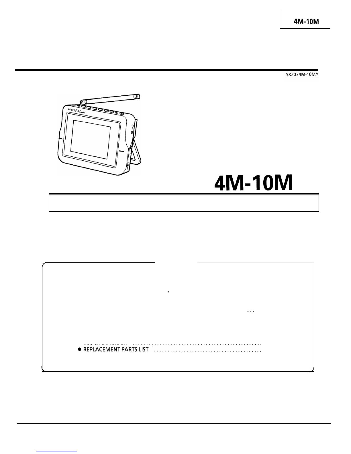
LCD COLOUR TELEVISION
MODEL
In the interests of user-safety (Required by safety regulations in some countries ) the set should be
restored to its original condition and only parts identical to those specified should be used.
CONTENTS
Page
l
IMPORTANT SERVICE SAFETY PRECAUTION
. . . . . . . . . . . . . . . . . . . . . . . . . .
2
l
ELECTRICAL SPECIFICATIONS
. . .
. . . . . . . . . . . . . . . . . . . . . . . . . . . . . . . . . . .
3
l
LOCATION AND IDENTIFICATION OF CONTROLS
. . . . . . . . . . . . . . . . . . . . . .
4
l DISASSEMBLY AND REASSEMBLY
. . . . . . . . . . . . . . . . . . . . . . . . . . . . . . . . . . .
5
l
TROUBLE SHOOTING TABLE . . . . . . . . . . . . . . . . . . . . . . . . . . . . . . . . . a.. . . . .
6
l
ADJUSTMENT PROCEDURES
. . . . . . . . . . . . . . . . . . . . . . . . . . . . . . . . . . . . . . . .
8
l
CHASSIS LAYOUT . . . . . . . . . . . . . . . . . . . . . . . . . . . . . . . . . . . . . . . . . . . . . . . . .
11
l
SCHEMATIC DIAGRAM AND WAVEFORMS
. . . . . . . . . . . . . . . . . . . . . . . . . .
13
l
PRINTED WIRING BOARD ASSEMBLIES
. . . . . . . . . . . . . . . . . . . . . . . . . . . . . .
19
. BLOCK DIAGRAM
25
27
. PACKING OF THE SET
. . . . . . . . . . . . . . . . . . . . . . . . . . . . . . . . . . . . . . . . . . . . .
37
SHARP CORPORATION
Page 2
IMPORTANT SERVICE SAFETY PRECAUTION
n Service work should be performed only by qualified service technicians who are
thoroughly familiar with all safety checks and servicing guidelines which follow:
WARNING
For continued safety, no modification of any
circuit should be attempted.
Disconnect AC power before servicing.
Any reading of
volt
(this corresponds
to
milliamp. AC.) or more is excessive and
indicates a potential shock hazard which must
be corrected before returning the receiver to
the owner.
BEFORE RETURNING THE RECEIVER
(Fire &Shock Hazard)
Before returning the receiver to the user,
perform the following safety checks:
Inspect all lead dress to make certain that leads
are not pinched, and check that hardware is
not lodged between the chassis and other
metal parts in the receiver.
Inspect all protective devices such as non-
metallic control knobs, insulating materials,
cabinet backs, adjustment and compartment
covers or shields, isolation resistor-capacity
networks, mechanical insulators, etc.
To be sure that no shock hazard exists, check
for current leakage in the following manner.
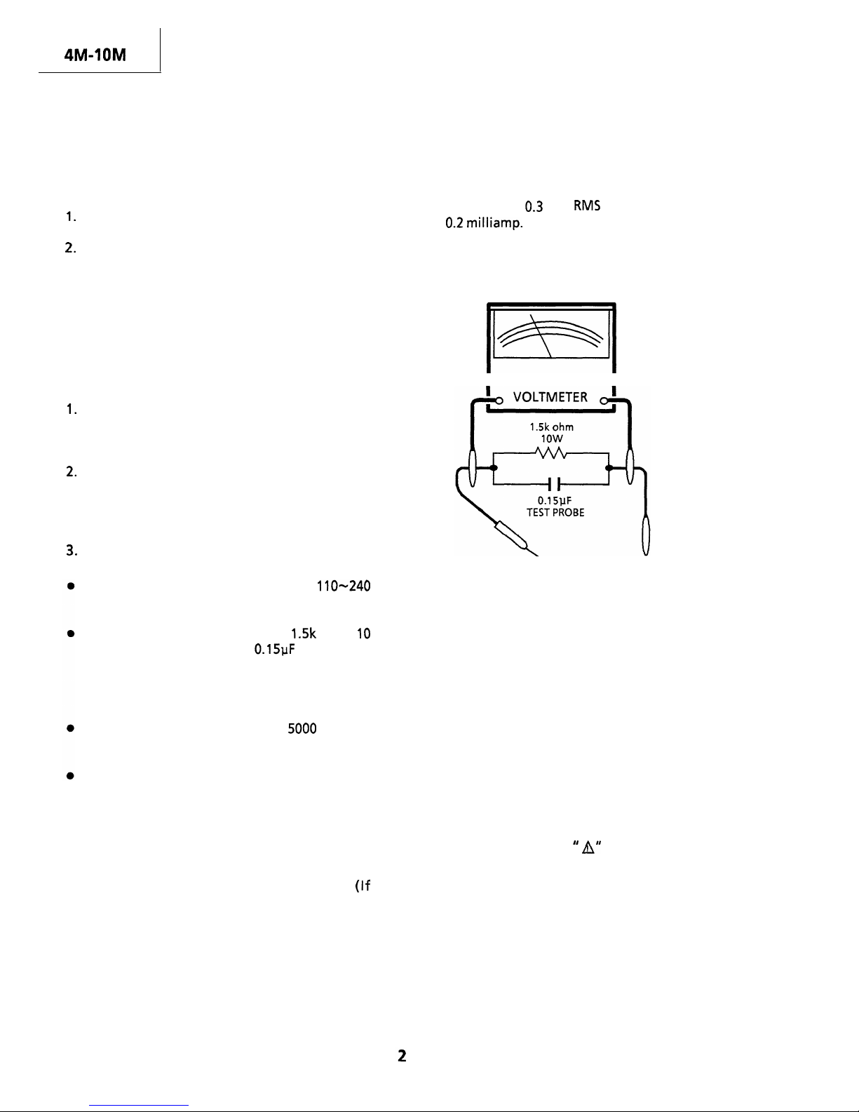
Plug the AC Adaptor directly into a
volt AC outlet, (Do not use an isolation
transformer for this test).
Using two clip leads, connect a
ohm,
watt resistor paralleled by a
capacitor in
series with all exposed metal cabinet parts and
a known earth ground, such as electrical
conduit or electrical ground connected to an
earth ground.
Use an AC voltmeter having with
ohm per
volt, or higher, sensitivity to measure the AC
voltage drop across the resistor.
Connect the resistor connection to all exposed
metal parts having a return path to the chassis
(antenna, metal cabinet, screw heads, knobs
and control shafts, escutcheon, etc.) and
measure the AC voltage drop across the
resistor.
All checks must be repeated with the AC
Adaptor plug connection reversed.
necessary, a nonpolarized adapter plug must
be used only for the purpose of completing
these checks.)
I
AC
I
TO EXPOSED’
CONNECT TO
METAL PARTS
KNOWN EARTH
GROUND
SAFETY NOTICE
Many electrical and mechanical parts in television
receivers have special
safety-related
characteristics.
‘These characteristics are often not evident from
visual inspection, nor can protection afforded by
them be necessarily increased by using
replacement components rated for higher
voltage, wattage, etc.
Replacement parts which have these special
safety characteristics are identified in this
manual; electrical components having such
features are identified by and shaded areas
in the Replacement Parts Lists and Schematic
Diagrams.
For continued protection,
replacement parts must be identical to those used
in the original circuit.
The use of a substitute
replacement parts which do not have the same
safety characteristics as the factory recommended
replacement parts shown in this service manual,
may create shock, fire, or other hazards.
Page 3
ELECTRICAL SPECIFICATIONS
Model
TV screen
Screen Size
LCD Panels
Drive method
Number of pixels
Receiving frequency
Audio output
Speaker
Light source
Terminals
Power supply
Power consumption
Dimensions (W x H x D)
Weigh
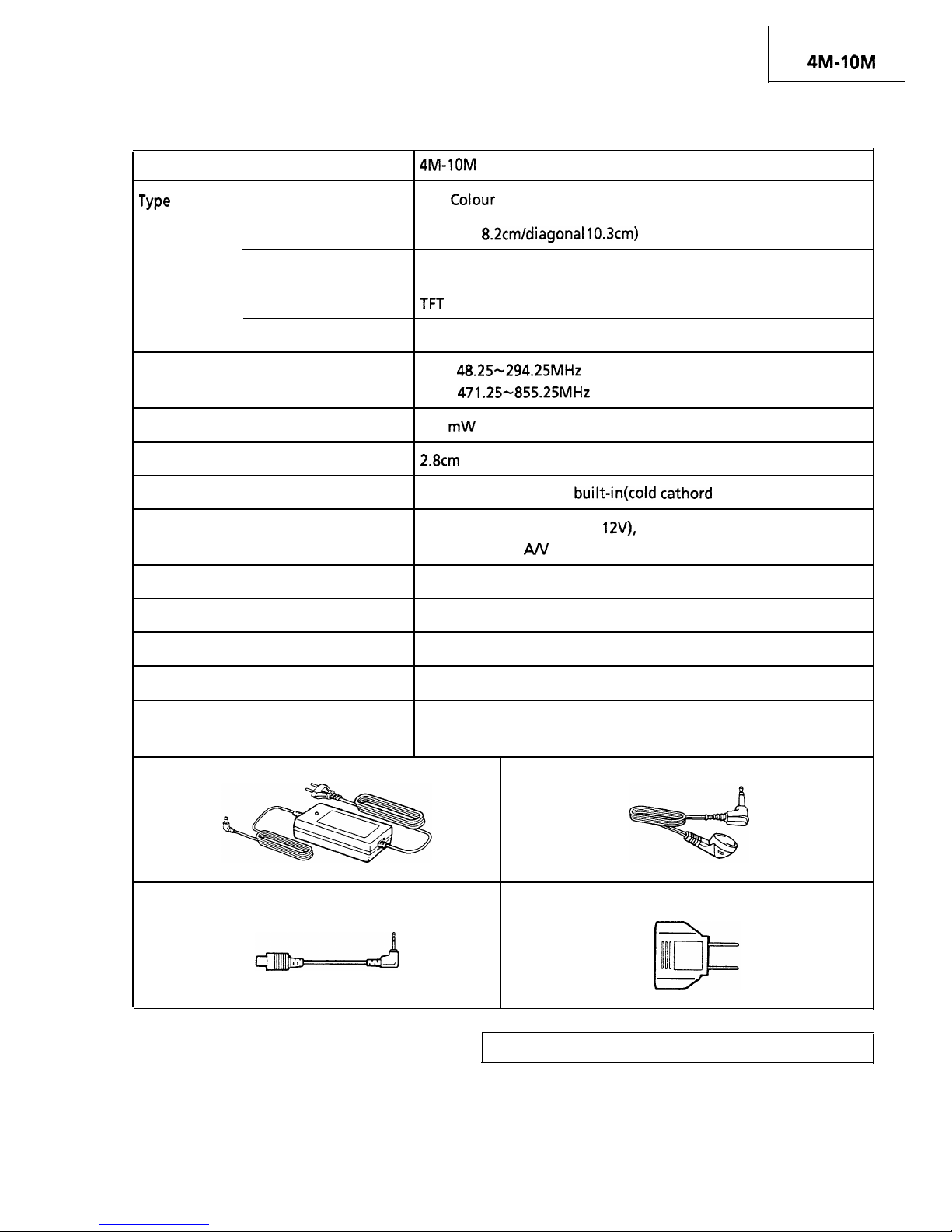
Supplied Accessories
AC Adaptor (1)
LCD
TV
4” (6.2 x
Transmission TN LCD panel
(Thin Film Transistor) active matrix system
37,440
(117
x 320)
VHF:
UHF:
200 mW
round type x 1
Fluorescent light tube, built-in(cold cathord type)
External power supply (DC
External antenna jack,
Earphone jack,
Input jack, Driver output jack
AC 110~240V 50/60Hz (AC adaptor supplied)
When using AC adaptor: Approx. 11 W (AC)
15.9x11.1 x 5.5cm
Approx. 570g (not including Set Stand)
AC Adaptor (1), Earphone (1), Antenna Adaptor (1), Adaptor
Socket plug(1)
Earphone (1)
Antenna Adaptor (1)
Adaptor Socket Plug (1)
Specifications are subject to change without notice
3
Page 4

LOCATION AND
OF CONTROLS
External antenna socket
Speaker
AN input
Diversity socket
Earphone jack
Video input indicator
Tint control
Colour control
Colour/Sound AUTO indicator
Mounting socket
Channel
buttons
Channel Number Recall button
Power switch
Mode switch
Set Memory button
System switch
DC power socket
Volume V
A buttons
Brightness V
A buttons
System change button
Rod antenna
Set stand
I LCD screen panel
4
Page 5
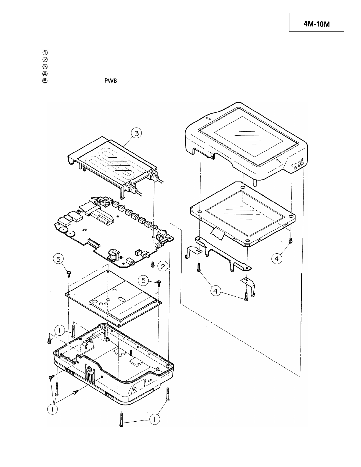
DISASSEMBLY AND REASSEMBLY
Remove the 7 rear cover fastening screws.
Remove the light guide fastening screws.
Undo the 3 light guide hooks.
Remove the 4 LCD holder fastening screws.
Remove the 4 Tuner
fastening screws.
5
Page 6
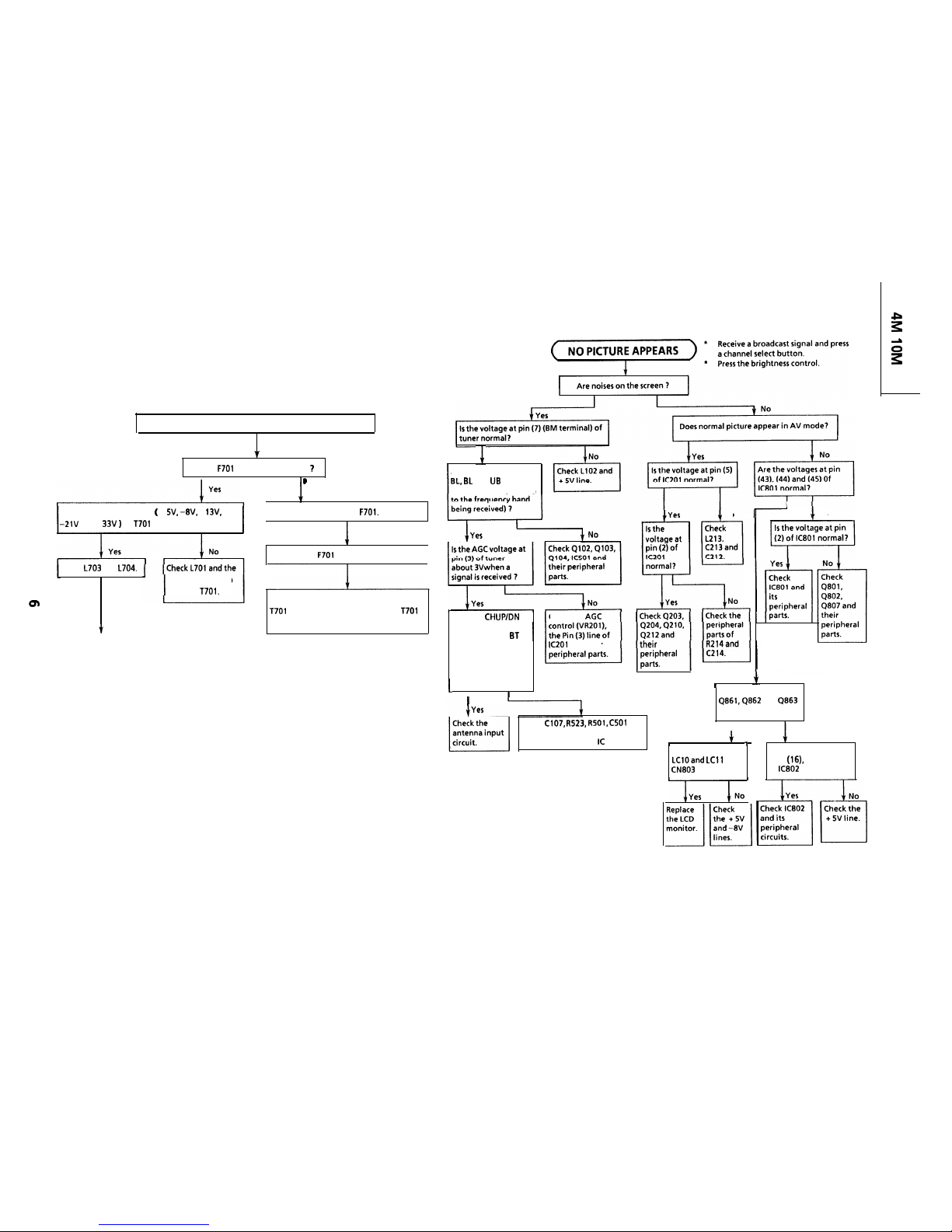
TROUBLE SHOOTING TABLE
(Continued)
Prior checks:
TROUBLE SHOOTING TABLE
I
NEITHER IMAGE NOR SOUND COMES OUT
Yes
Are voltages applied at
and
terminals
of tuner (corresponding
Is fuse
normally functioning
No
Replace fuse
Fuse
easily blows out.
1
Check the peripheral parts of 5701 and
as well as the secondary load of
for a short-circuit.
Are the secondary outputs
+ +
and + 33V
of
all normal?
I
No
No
Check
and
primary oscillation
circuit of T701.
Push the
buttons in search
mode. Does the
voltage at pin (4) of
tuner change?
Does the voltage go
up as the channel
,
numbers go up ?
Check the
and their
Continued to the following pages
Yes
Are the voltages of
and
normal?
I
No
Yes
Are the voltages at
Are the voltages at
LCll of
pins
(19) and (30)
normal?
of
normal ?
No
Check
and their peripheral parts, as well
as the Pin (20) line of
401.
Page 7
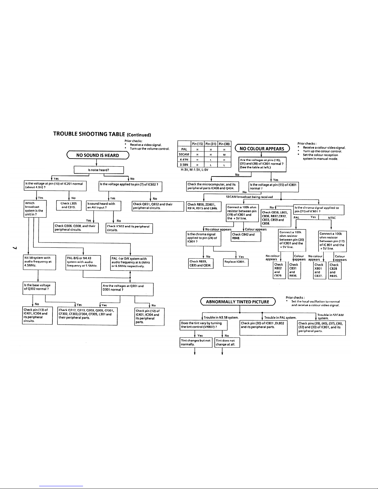
TROUBLE SHOOTING TABLE
(Continued)
TROUBLE SHOOTING TABLE
(Continued)
Prior checks:
NO SOUND IS HEARD
Page 8

ADJUSTMENT PROCEDURES ADJUSTMENT PROCEDURES
(Continued )
I
Adjusting Conditions
l
ADJUSTMENT : 1301
Adjusting Procedures
1. Feed colour bar signal.
(Set the input field strength to 58dBp)
2. Connect a the DC voltage meter to
1. Adjust
so that the voltage at TP205 be
I
Adjusting Conditions Adjusting Procedures
. + B ADJUSTMENT :
1. Connect the DC voltage meter to
1. Adjust
so that the +
line becomes
5
0.05v.
l
ADJUSTMENT : L209
1. Feed sweep signal to
2. Add fixed bias to
(Pin (1) of IC201)
I
1. Adjust 1209 to make the
marker as low
as possible.
l
SIGN POSlTlON ADJUSTMENT :
and
3. Connect an oscilloscope to
1. Using the
button, make
on
screen.
2. Adjust
to
position the “20-20” sign as
1. Feed colour bar signal.
(Set the input field strength to 58dBp)
2. Set the MODE switch 5401 to MEMORY (0)
position.
l
AFT ADJUSTMENT : L210
20-20’
1. Feed IF sweep signal to TPl 01.
2. Add fixed bias to
3. Connect the oscilloscope to
1. Adjust
so that the
marker be
positioned as shown below.
00
l
SIGN ADJUSTMENT : VR501
.
ADJUSTMENT :
1. Set the MODE switch 5401 to SEARCH
position.
2. Connect a diode and
ohm resistor between
pins (16) and (33) of
Set the unit to
MANUAL SEARCH mode.
1. Using the UP/DOWN key (A ,
set the channel
bar at the leftmost end of the VHF sign (just
before changing to the UHF sign).
See the figure below.
1. Feed colour bar signal.
(Set the input field strength to 58
2. Check the below
Sound mode : AUTO
1. Adjust
so that the voltage at
be
3
bar
. AFT FINE ADJUSTMENT :
1. Apply the output from the
(Signal Generator)
to the TPlOl.
(Output from
: 38.9MHz
1. With the tuning in UP search mode, adjust
so
that the voltage at
be 2.25V.
ohm
3. Connect pin (24) of
to the +
line and cut
off the AFT.
2. Adjust
so that the tuner’s
voltage at pin
(4) be 0.2V
O.lV.
Page 9
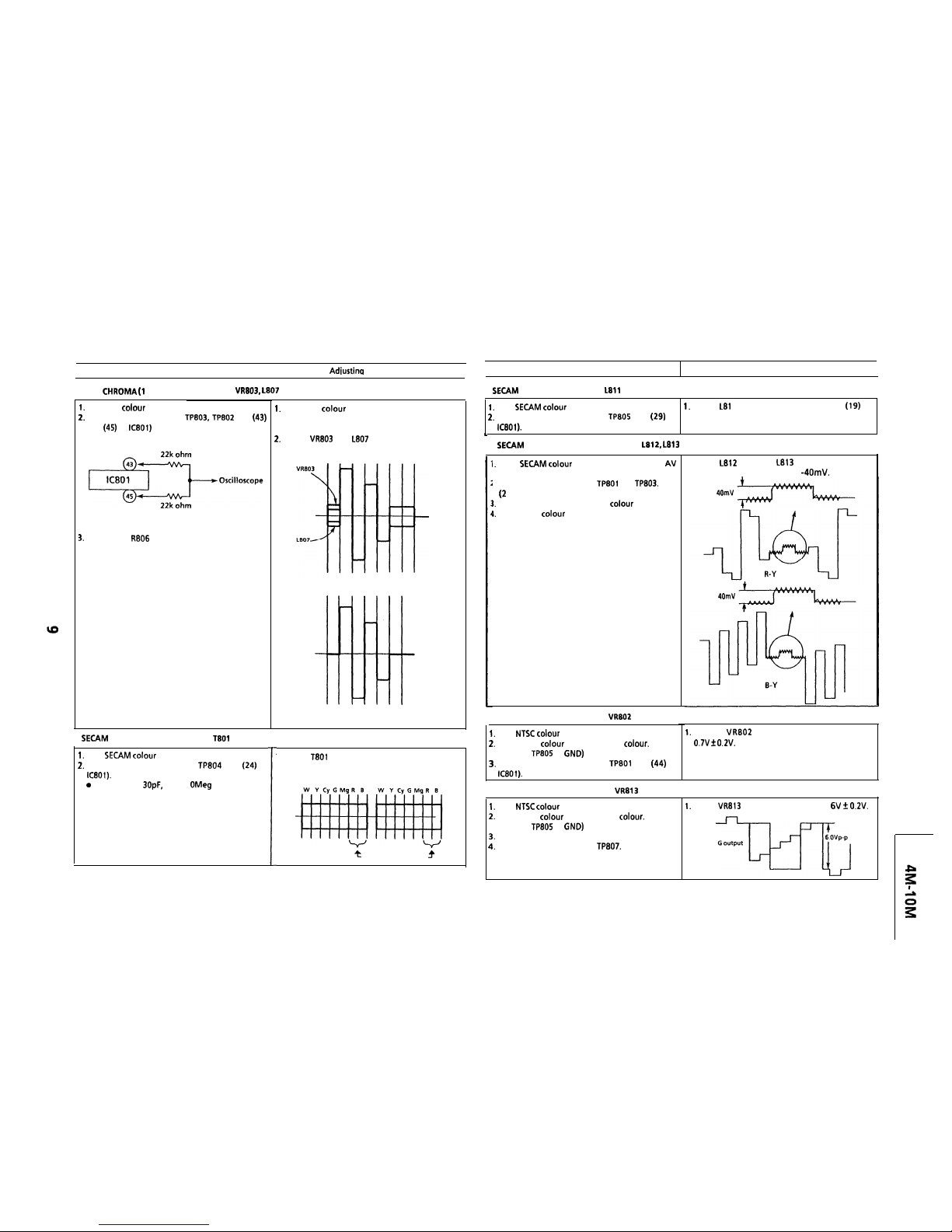
ADJUSTMENT PROCEDURES
(Continued)
I
Adjusting Conditions
I
I
l
PAL CHROMA
H DELAY) ADJUSTMENT : VR803,
Feed PAL colour bar signal.
Connect an oscilloscope to
TP802 (pin (43)
and (45) of IC801) with a resistor, one for each, in
between.
Short-circuit
to cut off the Y signal.
.
ADJUSTMENT : BELL FILTER
Feed
colour bar signal.
Connect the oscilloscope to
(pin
of
Over 1
ohms.
Turn the
control to make the biggest
difference between the green and magenta
levels.
Adjust
and
to obtain the waveform
shown at bottom.
Waveform before adjustment
Waveform after adjustment
I. Adjust
so that the R and B levels be the
same.
To be at the same level
ADJUSTMENT PROCEDURES
(Continued )
I
Adjusting Conditions
Adjusting Procedures
I
.
KILLER ADJUSTMENT :
Feed
colour bar signal.
Adjust
1 so that the DC level at pin
be
Connect the oscilloscope to
(pin
of
maximum.
l
DEMODULATION ADJUSTMENT :
Feed
bar signal through the AV
jack.
I. Connect the oscilloscope to
and
Channels)
Cut off the Y component of the colour bar signal.
Turn up the colour control all the way.
l
VIDEO OUTPUT ADJUSTMENT : VR802
Feed
bar signal.
Turn on the colour killer to turn off colour.
(Connect
to
Connect the oscilloscope to
(pin
of
. SUB BRIGHTNESS ADJUSTMENT : VR813
Feed
colour bar signal.
Turn on the colour killer to cut off
(Connect
to
Set the brightness control in middle position.
Connect the oscilloscope to
I. Adjust
(B-Y) and
(R-Y) so that the DC
level of R-Y and
B-Y signals be -40 mV.
Adjust VR802 so that the white level be
Adjust VR813 so that the amplitude be 6V
0.2V.
Page 10

ADJUSTMENT PROCEDURES
(Continued
Adjusting Conditions
I
Adjusting Procedures
CONTRAST ADJUSTMENT :
Take the standard settings.
Set the brightness
Adjust
so that the white level be 4V
0.2V.
control to middle position.
Feed
colour bar signal through the
jack.
Turn on the colour killer to turn off
[Standard settings]
Press the
+
side of BRIGHT and VOLUME keys.
Connect the oscilloscope to
Press the MEMORY,
and MEMORY keys
in this order.
. R-WHITE BALANCE ADJUSTMENT : VR810, VR812
Feed monoscope pattern signal through the AV
Turn
and
until the peak-to-peak
jack.
amplitude of the waveform on the oscilloscope
Set the brightness control to middle position.
screen becomes minimum.
Connect the oscilloscope to -out).
Connect the
cable of the oscilloscope to
Invert the waveform of
and add the
signal of channel-l to the channel-2.
. B-WHITE BALANCE ADJUSTMENT : VR807, VR806
Feed monoscope pattern signal through the AV
jack.
Set the brightness control to middle position.
Connect the oscilloscope to
(G-out) (Cl-t-l).
Connect the
cable of the oscilloscope to
Invert the waveform of
and add the
signal of channel-l to the
Turn
and
until the peak-to-peak
amplitude of the waveform on the oscilloscope
screen becomes minimum.
. COUNTER ELECTRODE BIAS ADJUSTMENT : VR814
Feed 1 O-tone black-and-white pattern signal.
Set the brightness control to middle position.
Turn
until the contrast gets sharpest.
l
SUB-BRIGHTNESS ADJUSTMENT : VR813
Feed lo-tone black-and-white pattern signal.
Set the brightness control to middle position.
Turn
until the second tone on the scale
gets whitish on the screen.
Page 11
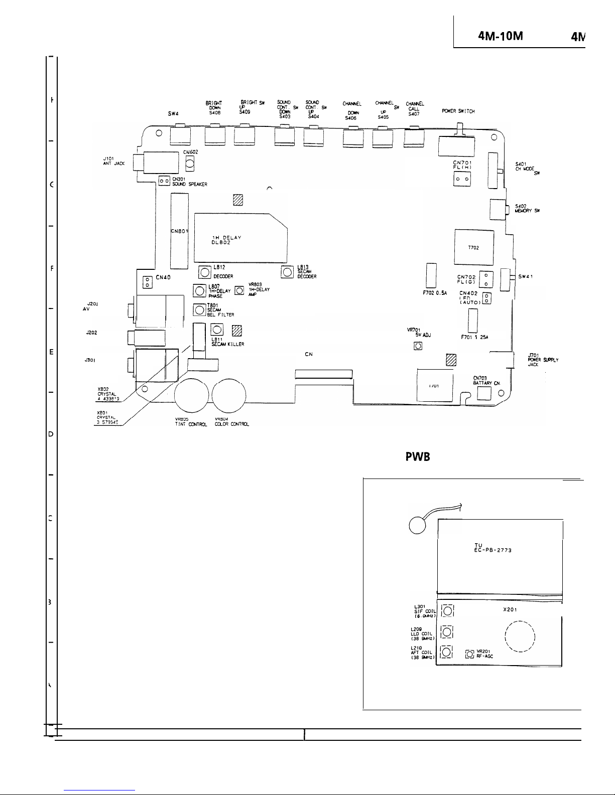
CHASSIS LAYOUT
SYSTEM
SW BRlGKi
CHANGE SW
SELECT
SELECT SW
5701
U
(Component Side)
1
SEW
1
LED
(A/V)
SELECT
0
0 0
DC
2%
1
SYSTEM
DIVERSITY JACK
LCD MODULE
EARPHONE JACK
L-
1
. TUNER
SELECT SW
1
0
101 TUNER
SAW FILTER
I
J
1 I
2
I
3
4
I
5
I
6
I
11
Page 12

0
(Wiring Side)
0
0
0
. LED
LED A/V
O
(GREEN)
0407
LED AUTO
‘I-
0
0
7
I
8
I
9
I
10
I
11
I
12
12
Page 13

SCHEMATIC DIAGRAM AND WAVEFORMS
n
Voltages were measured with a 20k ohm tester under the following conditions; supply voltage at AC
1
Hz), colour bar signal input from servicing colour bar signal generator, and
adjustment controls at their best positions.
n
Waveforms were observed with colour bar signal input from servicing colour bar signal generator and
controls at their
best positions.
0
2
0
3
Audio
0
4
Blue
0
5
Green
9 9Vp-p
R-Out
10
11
2O@div
H. Sync
12
2O@div
0
14
DC-AC Drive
0
15
0
16
DC-AC Out
13
Page 14

SCHEMATIC DIAGRAM
AC ADAPTOR
AND SHADED
) COMPONENTS
SAFETY RELATED PARTS.
1
I
2
I
3
I
4
5
I
6
Page 15

SCHEMATIC DIAGRAM
MAIN
I
I I
1
I
2
I
3
4
I
5
I
6
I
7
Page 16

I
I
I
I
I
I
I
I
I
I
I
t
I
I
I
6
I
7
I
8
I
9
I
I
I
Page 17

SCHEMATIC DIAGRAM
TUNER
---
--
RI
120
0502
i
I
0103
I
I
Page 18

t
CL
AFT/BAND/TUNING
L-------l
T
I
3
I
7
I
8
9
I
I
I
I
Page 19

PRINTED WIRING BOARD ASSEMBLIES
l
MAIN
(Component Side)
Page 20

l
LED
(Component Side)
I
8
I
9
I
10
I
11
I
12
20
Page 21

l
MAIN
(Wiring
Side)
1
I
2
I
3
I
4
I
5
I
6
21
Page 22

l
LED
(Wiring Side)
7
I
8
I
9
I
I
I
I
Page 23

.
PRINTED WIRING BOARD ASSEMBLIES (Continued)
l
TUNER
(Component Side)
1
I
2
I
3
I
4
I
5
I
6
Page 24

I
TUNER
(Wiring Side)
7
I
8
I
9
I
I
I
I
Page 25

L
41
BLOCK DIAGRAM
I
I
AUDIO
1
1
I
2
3
I
4
5
I
25
Page 26

I
KEY MATRIX
i
I I
iii
7
4
3
2
I
TO
I
7
I
8
I
9
I
I
I
Page 27

PARTS LIST
PARTS REPLACEMENT
Replacement parts which have these special
characteristics
in this manual: electrical components having such
Features are
by
in the Replacement Parts Lists.
The use
a substitute replacement part which does not have
the same
characteristics as the Factory recommended
replacement parts shown in this service manual may create
shock, Fire or other hazards.
“HOW TO ORDER REPLACEMENT PARTS”
To have your order Filled promptly and correctly, please Furnish
the Following informations.
1. MODEL NUMBER 2. Ref. No.
3. PART NO. 4. DESCRIPTION
MARK
SPARE PARTS-DELIVERY SECTION
I
Ref. No.
I
Part No.
I I
Description
I
PRINTED WIRING BOARD ASSEMBLIES
( NOT REPLACEMENT ITEM )
J
J
J
LED PWB Unit
UNIT PARTS
J LCD Module Unit
**
MAIN
UNIT
1
INTEGRATED CIRCUITS
J
J
J
J
J TC7SOBF
J
J
J
J
J
J
AH
AK
AM
AK
AZ
FLUORESCENT LAMP
J
AZ
Ref. No.
Part No.
I I
Description
Code
4403
4404
4405
4407
4601
4701
4751
4753
4754
4757
TRANSISTORS
J
J
J
J
J
J
J
J
J
J
J
J
J
J
J
J
J
J
J
5
J
J
J
J
J
J
J
J
J
J
J
J
J
J
J
DIODES
J
J
J
J
J
J
J
J
J
J
J
J
J
J
J
J
J
J
AC
AD
AC
AC
AC
AC
AC
AC
AC
AC
AC
AC
AC
AC
AD
AD
AC
27
Page 28

I
Ref. No.
Part No.
Description
Code
Ref. No.
Part No.
Description
Code
MAIN
UNIT
(Continued)
DIODES
(Continued )
J
J
J
J
J
J Thermistor
AD
AD
AC
PACKAGED CIRCUITS
J Delayline
J Delayline
J Crystal
J Crystal
J Crystal
J Crystal
AD
AK
COIL AND TRANSFORMERS
J
33016 J
1701
Al
J
Coil (Chip)
J
J
Coil (Chip)
J
J
Coil (Chip)
J
J
Coil (Chip)
J
J Coil (Chip)
J
Coil (Chip)
J
J
Coil (Chip)
J Coil (Chip)
J Coil (Chip)
J Coil (Chip)
J
J
Coil (Chip)
J Coil
J Trans. DC-DC
J Trans. DC-AC
J Trans.
AC
AD
AD
CONTROLS
J
J
AD
J
J
1H Delay
AD
J
AH
J
AH
J
AE
J lOOK(B)SBright(B) AE
J
AE
J
CONTROLS
(Continued)
J
AE
J
J
CAPACITORS
J
Ceramic AB
JC J
Ceramic AB
J
Ceramic AB
J
Ceramic AB
JC J
Ceramic AB
JC J
Ceramic AB
J
Ceramic AB
J
Ceramic AB
J 1pF
Electrolytic AE
J 0.1,~F
Ceramic AB
J 0.01,~F
Ceramic AB
J 0.1,~F
Electrolytic AE
J 22OpF
Ceramic AB
J 22OpF
Ceramic AB
J 3.3,~F
Electrolytic
JC J
Ceramic AB
J
Ceramic AB
JC J
Ceramic AB
J 22OpF
Ceramic AB
J
Ceramic AB
21 JC J 12OpF
Ceramic
21 JC J 12OpF
Ceramic
J 0.01/~F
Ceramic AB
J
J 0.01,~F
Ceramic AB
J
Ceramic AB
1
121
J 12OpF
Ceramic AB
21
J 12OpF
Ceramic
J
Ceramic AB
J
Ceramic AB
J 22OpF
Ceramic AB
JC J 22OpF
Ceramic AB
J
Ceramic
Ml J 33OpF
Electrolytic AF
J
Electrolytic AD
J
Electrolytic AE
J
J 0.01,~F
Ceramic
MT J 100,~F
Electrolytic AC
J 330,~F
Electrolytic AF
J 0.01,~F
Ceramic
J 0.1,~F
Ceramic AB
MT J
Electrolytic AC
J
J
Electrolytic AE
J 330,~F
Electrolytic
J 0.01,~F
Ceramic
J
Electrolytic AE
J
Electrolytic
J 22OOpF
J
Ceramic AB
J 18OpF
Ceramic AB
J 18OpF
Ceramic AB
J
Ceramic AB
Page 29

I
Ref. No.
I
No.
I I
Description
I
Code
MAIN
UNIT
(Continued)
1
J
Electrolytic AE
J
Ceramic AB
J
Ceramic AB
F J
J
Ceramic AB
J
Ceramic
J
Ceramic
MT J
Electrolytic AD
J
MT J
J 0.1,~F
Ceramic AB
J 47,uF
Electrolytic AE
J
AB
J
KB J
Ceramic
J 1pF 1OV Tantalum AD
J
Ceramic AB
J 1pF 1OV Tantalum AD
J
Ceramic AB
J 1OpF 1OV Electrolytic AE
J
Ceramic AB
J
J
Ceramic AB
J
Ceramic AB
J
Ceramic AB
J
Ceramic AB
J
J
J 10/1F
1
J
J
Ceramic AB
CAPACITORS
(Continued )
J
Ceramic AB
JC J 15OpF
Ceramic
J
AB
J
1 M 1 J
AF
J 0.68,~F
Ceramic AC
J
Ceramic AB
J
Electrolytic AE
J
Electrolytic AE
J
Electrolytic AD
J
Ceramic AB
J
J
Ceramic AB
1 M 1 J 330,~F
AF
J
Ceramic AB
J 0.01,~F
Ceramic AB
J 100,~F
Electrolytic AC
J
Electrolytic
JC J 330,~F
Ceramic
J
AB
J
AB
J 0.01,~F
Ceramic AB
J
Ceramic AB
J 330,~F
Electrolytic AF
J
Electrolytic
CAPACITORS
(Continued
J
1OV Tantalum
J I,uF
Electrolytic
J
1 OV Electrolytic
J
Ceramic
J
Ceramic
J
Ceramic
J
Ceramic
J
Ceramic
J
Ceramic
J
Ceramic
J
Ceramic
J
Ceramic
J
Ceramic
J 0.1,~F
Ceramic
J
Ceramic
J
J
Ceramic
J 0.01,~F
Ceramic
J
Ceramic
J
Ceramic
J
Ceramic
J 0.01,~F
Ceramic
J
Ceramic
J
1 OV Electrolytic
J
Ceramic
J
Ceramic
J
Ceramic
J 22OpF
Ceramic
1
J 12OpF
Ceramic
J 2OpF
Ceramic
J
Ceramic
J 2OpF
Ceramic
J
Ceramic
J
Ceramic
J
Ceramic
J
Ceramic
J 0.1,~F
Ceramic
J
Ceramic
J
Ceramic
J
Ceramic
J 47,uF
Electrolytic
J
Ceramic
J 0.1,~F
Ceramic
J
Ceramic
KB J 82OpF
Ceramic
1
J 15OpF
Ceramic
J
Ceramic
J
Ceramic
J
Ceramic
J 47/~F
Electrolytic
J
Ceramic
J
Ceramic
J
Ceramic
J
Ceramic
J
Ceramic
J
Ceramic
J 0.1,~F
Ceramic
J 0.1,~F
Ceramic
J 0.1,~F
Ceramic
1 MT J
Electrolytic
J 0.1,~F
Ceramic
AD
AC
AD
AC
AC
Page 30

--
Ref. No.
Part No.
Description
Code
Ref. No. Part No.
Description
Code
MAIN
UNIT (Continued)
CAPACITORS
(Continued )
J
1 OV Tantalum
J 2.2,uF 1OV Tantalum
J
Ceramic
J
Ceramic
J
Ceramic
AD
AD
RESISTORS
J 100
Chip
J 100
Chip
J 100
Chip
J 100
Chip
J 100
Chip
J
Chip
J
Chip
J
Chip
J
Chip
J
Chip
J 100
Chip
J
Chip
J 390
Chip
J
Chip
J
Chip
J
Chip
J
Chip
J
Chip
J
Chip
J
Chip
1
J
Chip
J
Chip
J
Chip
J
Chip
J
Chip
J
Chip
J
Chip
J
Chip
J 100
Chip
J 100
Chip
1
J 100
Chip
J 390
Chip
1
J
Chip
J
Chip
J
Chip
J
Chip
J
Chip
J
Chip
J
Chip
J
Chip
J
Chip
J
Chip
J
Chip
J
Chip
J
Chip
J
Chip
J
Chip
I
I
I
I
I
RESISTORS
(Continued
J
Chip
J
Chip
J
Chip
J
100
Chip
J
Chip
J
Chip
J
Chip
J
Chip
J
Chip
J
Chip
J
Chip
J
Chip
J 33
Chip
J
J 33
Chip
J 33
Chip
J 33
Chip
J 0
Chip
J
Chip
J
Chip
J
Chip
J
Chip AB
J 100
J
Chip
J 68
Chip AB
J 68
Chip
J
Chip
J 10
Chip
J 33
Chip
J
Chip
J
Chip
J
Chip
J 1
Chip
J 10
Chip AB
J 680
Chip
J 680
Chip
J
Chip
J 100
J
Chip AB
J 8.2
Chip AB
J 3.3
Chip AB
J
Chip
J 10
Chip
J
Chip
J
Chip
J
Chip AB
J
Chip AB
J
Chip AB
J
Chip AB
J
Chip AB
J
Chip AB
J
Chip AB
J
Chip AB
J
Chip AB
J 220
l/l
Chip
J
Chip AB
J 3.9
Metal
J
Chip AB
J
Chip AB
1 1
J 510
Chip AB
J
Chip AB
30
Page 31

Ref. No.
Description
Code
Ref. No. Part No.
Description
Code
MAIN
UNIT
(Continued)
1
1
RESISTORS
(Continued )
J
J
J
J
J
J
J
J
J
J
J
J
J
J
J
J
J
J
J
J
J
J
J
J
J
J
J
J
J
J
J
J
J
Chip
Chip
Chip
Chip
Chip
Chip
Chip
Chip
Chip
Chip
Chip
Chip
Chip
Chip
Chip
Chip
Chip
Chip
Chip
Chip
Chip
Chip
Chip
Chip
Chip
Chip
Chip
Chip
Chip
Chip
Chip
Chip
Chip
Chip
Chip
Chip
Chip
Chip
Chip
Chip
Chip
Chip
Chip
Chip
Chip
Chip
Chip
Chip
Chip
Chip
Chip
Chip
Chip
Chip
Chip
Chip
Chip
Chip
1
RESISTORS
(Continued )
J
Chip
Chip
J
Chip
Chip
J
Chip
J
Chip
J
Chip
J
Chip
J
Chip
J
Chip
J
Chip
J
Chip
J
Chip
J
Chip
J
Chip
J
Chip
J
Chip
J
Chip
J
Chip
J 12
Chip
J
Chip
J
Chip
J
Chip
J
Chip
J 0
Chip
J
Chip
J
Chip
J
Chip
MISCELLANEOUS PARTS
J
J
J
J
J
J
J
J
J
J
J
J
1
J
Up
J
Down
J
J
J
J
J
J
J
J
J
J
J
J
J
J
J Connector,
J
AL
AL
AH
AL
AL
AH
AD
AD
AD
AD
AD
AD
AD
AH
AH
AC
AC
AC
AC
AK
Page 32

Ref. No. Part No.
Description
Code
Ref. No. Part No.
Description
Code
TUNER
UNIT
(Continued)
TUNER
NOTE:
THE PARTS HERE SHOWN ARE SUPPLIED AS AN
ASSEMBLY BUT NOT INDEPENDENTLY.
J Tuner
INTEGRATED CIRCUITS
J
J
J
J TC74HCOOAF
J
AU
AH
TRANSISTOR
J
4102
J
4103
J
4104
J
J
4202
J
J
J
J
J
J
J
4212
J
J
4301
J
J
4303
J
4304
J
4305
J
J
4307
J*
J
4311
J
J
4313
J
J
J
AH
AC
AC
AC
AC
AC
AC
AC
AC
AC
DIODES
J
J
J
0203
J
J
J
J
J
AC
AD
AD
AC
AC
AC
AC
AC
PACKAGED CIRCUITS
J
J Crystal
J Crystal
AT
AD
AC
COILS AND TRANSFORMERS
J
J
J
J
J
J
J
J
J
J
J
J
J
J
J
J
J
J 27,~H
J
J
J
J
J
J 2.2,~H
J
221
J
J
J
J
AD
AD
32
Page 33

Ref. No.
Part No.
Description
Code
Ref. No.
Part No.
Description
Code
r
CAPACITORS
(Continued)
TUNER
UNIT
(Continued)
CONTROLS
J
AE
J
Ceramic AC
J
Ceramic AC
J
Ceramic AB
J
Ceramic AC
J
Electrolytic AD
J
AB
J 47,~F
AE
J
Ceramic AB
J
Ceramic AB
J
J
Ceramic AC
J
Ceramic AB
1 J
AD
J
Ceramic AB
J
Electrolytic AD
J
Electrolytic AD
J
Ceramic AB
J
Electrolytic AD
J
Ceramic AB
J 1pF
Electrolytic AD
J
Ceramic
J
Ceramic AB
J
J
CAPACITORS
J 15OpF
Ceramic
J
Ceramic AB
J
Ceramic AC
J
Ceramic AB
J
Ceramic AB
1
J 47,uF
Electrolytic AE
J
Tantalum AD
J
Ceramic AB
MT J 22OpF
AD
J
Ceramic AB
J
Ceramic AB
J
Ceramic AB
J
Ceramic AB
J
Ceramic AB
J
Ceramic AB
J
AF
J
Ceramic AB
J
Ceramic AB
J
Ceramic AB
J 22OOpF
Ceramic AB
J 22OOpF
Ceramic AB
J 22OOpF
Ceramic AB
J 22OOpF
Ceramic AB
J 22OOpF
Ceramic
J
Ceramic AB
J
Ceramic AB
J 47/1F
Electrolytic
J
Tantalum AD
J
Tantalum AD
J
Ceramic AB
J
Ceramic AB
J
Ceramic AK
J
Ceramic AB
J
Ceramic AK
J
Ceramic AB
J 1OpF
AC
J
Ceramic AB
J
Ceramic AB
J 22OOpF
Ceramic AB
J 22OOpF
Ceramic AB
J
Ceramic AB
J
Ceramic AB
J 560/~F
Ceramic AB
J
Ceramic AB
JC J
Ceramic AB
J 27OpF
Ceramic AB
J 22OOpF
Ceramic AB
J
Ceramic
J
J
Ceramic
J
Ceramic AB
RESISTORS
J
(Chip)
J
(Chip)
J
(Chip)
J
(Chip)
J
1 (Chip)
J
(Chip)
J
(Chip)
J
J
(Chip)
J
(Chip)
J
(Chip)
J
(Chip)
1
J
(Chip)
1
J
(Chip)
1
J
(Chip)
J
(Chip)
J
(Chip)
J
(Chip)
J
(Chip)
J
(Chip)
J
(Chip)
J
(Chip)
J
(Chip)
J
(Chip)
J
(Chip)
J
(Chip)
J
(Chip)
J
(Chip)
J
(Chip)
J
(Chip)
J
(Chip)
J
(Chip)
Page 34

TUNER
UNIT
(Continued)
RESISTORS (c
J
J
J
J
J
J
J
J
J
J
J
J
J
J
J
J
J
J
J
J
J
J
J
J
J
J
J
J
J
J
J
J
J
J
J
J
J
J
J
J
J
J
J
J
J
J
J
J
J
J
J
J
J
J
J
J
J
150
(Chip)
(Chip)
330
(Chip)
(Chip)
330
(Chip)
(Chip)
(Chip)
(Chip)
(Chip)
(Chip)
(Chip)
560
(Chip)
0
(Chip)
(Chip)
470
(Chip)
(Chip)
(Chip)
560
(Chip)
470
(Chip)
470
(Chip)
470
(Chip)
120
(Chip)
470
(Chip)
(Chip)
(Chip)
180
(Chip)
(Chip)
(Chip)
(Chip)
(Chip)
(Chip)
180
(Chip)
(Chip)
(Chip)
470
(Chip)
(Chip)
(Chip)
820
(Chip)
820
(Chip)
470
(Chip)
(Chip)
100
(Chip)
(Chip)
(Chip)
(Chip)
(Chip)
(Chip)
470
(Chip)
47
(Chip)
(Chip)
(Chip)
(Chip)
(Chip)
0
(Chip)
(Chip)
(Chip)
(Chip)
Ref. No.
Part No.
Description
Code
Ref. No.
Part No.
Description
Code
RESISTORS
(Continued)
J
(Chip) AB
J
(Chip) AB
J
(Chip) AB
J
(Chip)
J
(Chip)
J
(Chip) AB
J
(Chip)
J
(Chip)
J 0
(Chip) AB
J
(Chip) AB
J
(Chip)
J
(Chip) AB
J
(Chip) AB
J
J
(Chip) AB
J
(Chip)
J
(Chip)
J
(Chip) AB
J
(Chip) AB
J
(Chip)
MISCELLANEOUS PARTS
J
J Connector,
AT
LED
UNIT
DIODES
J
0408
J
RESISTORS
J
(Chip)
J 560
(Chip)
MISCELLANEOUS PARTS
1 Al J
pin
J
pin
J
AC
AC
AK
AK
Page 35

OM
H
G
F
E
D
C
B
CABINET AND MECHANICAL PARTS
1
I
2
I
3
I
4
I
5
6
1
35
Page 36

No.
Part No.
Description
Code
No.
Part No.
Description
Code
CABINET AND MECHANICAL PARTS
1
l-l
1
1-7
2
1 Al
3
4
5
6
7
8
9
10
11
12
13
14
15
16
17
18
19
20
21
22
23
24
25
26
27
28
29
30
31
32
33
34
35
36
37
38
39
40
41
42
43
44
J Cabinet Ass’y
J
J Button, Memory
J Knob, Mode
J Button, Ass’y
J Knob, Power
J Cover
J Spacer-B
Spacer-A
J Rear Cabinet
J Antenna Bracket
J Insulator Sheet
J Insulator Sheet
J Insulator Sheet
J Insulator Sheet
J Charge Lug
J Contact Spring
J Charge Lug
J Wire
J Flexible Connector
J Cushion
J Screw
J Screw
J Light Guide
J Shade Panel
J Fluorescent Lamp
J Trigger
J Shield Panel
J Side Cabinet
J Protect Panel
J Cushion
J LCD Unit
J Speaker
J LCD Bracket
J
LCD Earth Panel
J LCD Earth Panel
J Bracket
J Screw
J Screw
J Screw
J Screw
J Knob, System
J Shaft Guide
J Screw
J Light Cover
J Rod Antenna
J Set Stand
J Rubber Leg
J Model Label
J Pre Label
J Antenna Label
J Screw
AC
AC
AC
AD
AA
AA
BE
AD
AD
AD
AH
AC
AC
AS
AK
AC
AA
AZ
AD
AH
AT
AC
AC
AC
AA
AA
AC
AA
AU
AK
AK
AC
45
J Screw
46
J Screw
47
J Screw
48
J
SUPPLIED ACCESSORIES
ACCESSORIES
J
BP
J Earphone
J
J
AH
ACCESSORIES
(
NOT REPLACEMENT ITEM
)
Operation Manual
PACKING PARTS
Packingcase
Buffer material
Polystyrene cover
Cushion
Polystyrene cover
36
Page 37

PACKING OF THE SET
Polystyrene Cover
Earphone
Antenna
Adaptor Socket
Buffer Material
37
Page 38

SHARP
Printed in Japan
 Loading...