

Page 1
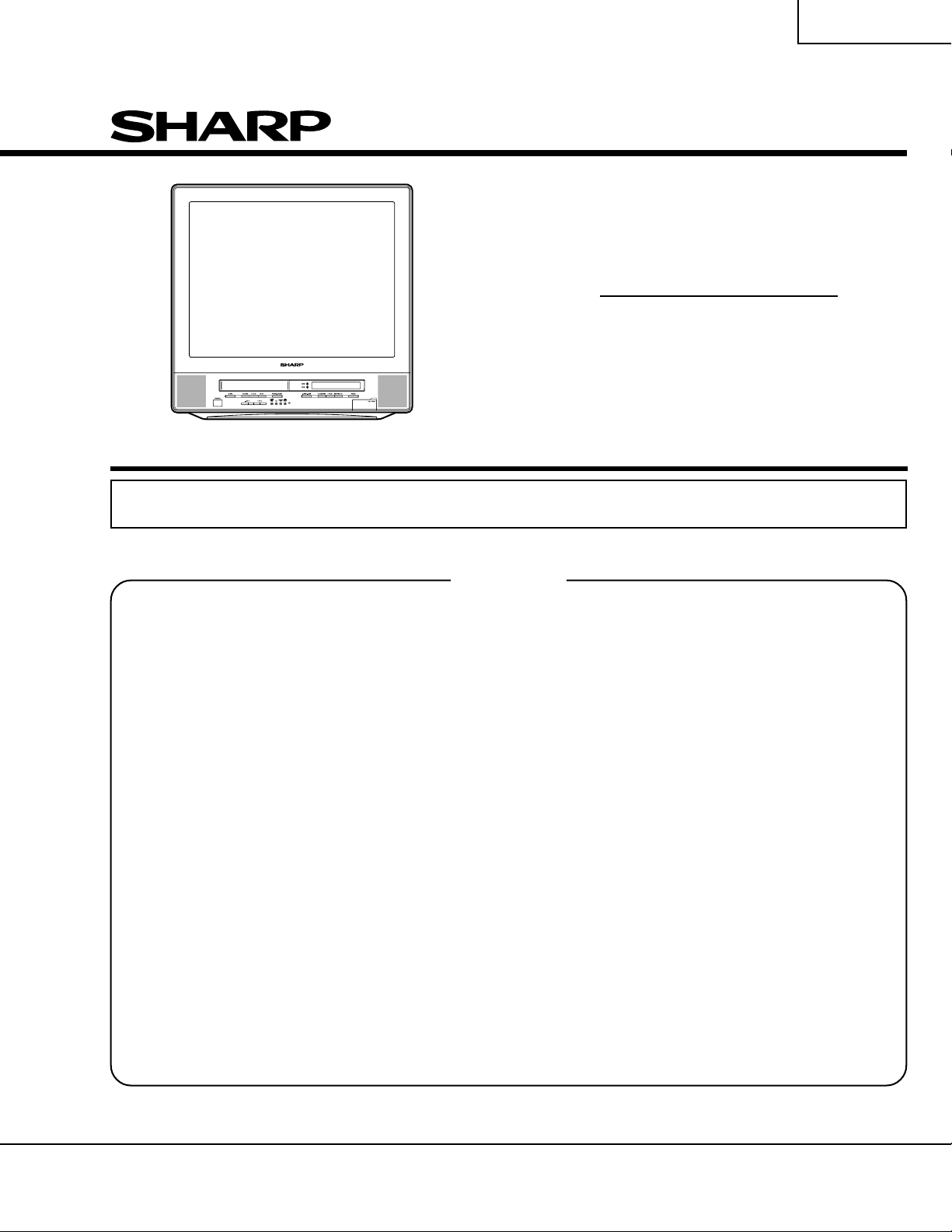
27DV-S100
27DV-CS10
SERVICE MANUAL
S81Z627DV-S10
TV/VCR/DVD COMBINATION
Chassis No. B00A
27DV-S100
MODELS
In the interests of user-safety (Required by safety regulations in some countries) the set should be restored
to its original condition and only parts identical to those specified should be used.
CONTENTS
» IMPORTANT SERVICE SAFETY PRECATION ....................................................................................... 2
» SAFETY PRECAUTIONS ........................................................................................................................ 6
» ELECTRICAL SPECIFICATIONS ............................................................................................................ 7
» LOCATION OF USER'S CONTROL ........................................................................................................ 8
» DISASSEMBLY AND REASSEMBLY..................................................................................................... 12
» INSTALLATION AND SERVICE INSTRUCTIONS ................................................................................. 16
» PRECAUTIONS IN REASSEMBLING ................................................................................................... 22
» FUNCTION OF MAJOR MECHANICAL PARTS.................................................................................... 23
» ADJUSTMENT, REPLACEMENT AND ASSEMBLY OF MECHANICAL UNITS.................................... 25
» ADJUSTMENT OF THE VCR ELECTRICAL CIRCUITRY..................................................................... 45
» TEST MODE OF DVD SECTION........................................................................................................... 47
» TROUBLESHOOTING........................................................................................................................... 50
» CHASSIS LAYOUT................................................................................................................................. 72
» IC FUNCTION LIST OF DVD SECTION ................................................................................................ 74
» BLOCK DIAGRAM OF TV SECTION.....................................................................................................94
» BLOCK DIAGRAM OF VCR SECTION .................................................................................................. 96
» BLOCK DIAGRAM OF DVD SECTION................................................................................................ 106
» OVERALL SCHEMATIC DIAGRAM ..................................................................................................... 108
» DESCRIPTION OF SCHEMATIC DIAGRAM....................................................................................... 110
» PRINTED WIRING BOARD ASSEMBLIES.......................................................................................... 143
» REPLACEMENT PARTS LIST ............................................................................................................. 155
» PACKING OF THE SET ....................................................................................................................... 185
27DV-CS10
Page
SHARP CORPORATION
This document has been published to be used for
after sales service only.
The contents are subject to change without notice.
1
Page 2
27DV-S100
27DV-CS10
IMPORTANT SERVICE SAFETY PRECAUTION
Ë Service work should be performed only by qualified service technicians who are thoroughly
familiar with all safety checks and servicing guidelines which follow:
WARNING
1. For continued safety, no modification of any circuit
should be attempted.
2. Disconnect AC power before servicing.
3. Semiconductor heat sinks are potential shock hazards
when the chassis is operating.
4. The chassis in this receiver has two ground systems
which are separated by insulation material. The nonisolated (hot) ground system is for the +B voltage
regulator circuit and the horizontal output circuit.The
isolated ground system is for the low +B DC v oltages
and the secondary circuit of the high voltage
transformer .
To prevent electrical shock use an isolation
transformer between the line cord and power
receptacle, when servicing this chassis.
CAUTION: FOR CONTINUED
PROTECTION AGAINST A
RISK OF FIRE, REPLACE
6.3A 125V
ONLY WITH SAME TYPE 6.3A125V FUSE.
SERVICING OF HIGH VOLTAGE SYSTEM
AND PICTURE TUBE
When servicing the high voltage system,
remove the static charge by connecting a
10k ohm resistor in series with an insulated
wire (such as a test probe) between the
picture tube ground and the anode lead. (A C
line cord should be disconnected from AC
outlet.)
1. Note that the picture tube in this receiver employs
integral implosion protection.
2. Replace with tube of the same type number for
continued safety.
3. Do not lift picture tube by the neck.
4. Handle the picture tube only when wearing
shatterproof goggles and after discharging the high
voltage anode completely.
X-RADIATION AND HIGH VOLTAGE LIMITS
1. Be sure all service personnel are aware of the
procedures and instructions covering X-radiation. The
only potential source of X-ray in current solid state
TV receivers is the picture tube. Howev er, the picture
tube does not emit measurable X-Ray r adiation if the
high voltage is as specified in the “High V oltage Check”
instructions.
It is only when high voltage is excessive that Xradiation is capable of penetrating the shell of the
picture tube including the lead in glass material. The
important precaution is to keep the high voltage below
the maximum level specified.
2. It is essential that servicepersonel have available at
all times an accurate high voltage meter.
The calibration of this meter should be checked
periodically.
3. High voltage should always be kept at the rated v alue
-no higher. Operation at higher voltages may cause
a failure of the picture tube or high voltage circuitry
and;also,under certain conditions, may produce
radiation that exceeds specifications.
4. When the high voltage regulator is operating properly
there is no possibility of an X-radiation problem. Every
time a color chassis is serviced, thebrightness should
be tested while monitoring the high voltage with a
meter to be certain that the high voltage does not
exceed the specified value and that it is regulating
correctly.
5. Do not use a picture tube other than that specified or
make unrecommended circuit modifications to the
high voltage circuitry.
6. When trouble shooting and taking test measurements
on a receiver with excessiv e high voltage , av oid being
unnecessarily close to the receiver.
Do not operate the receiver longer than is necessary
to locate the cause of excessive voltage.
2
Page 3
IMPORTANT SERVICE SAFETY PRECAUTION
2
2
(Continued)
27DV-S100
27DV-CS10
BEFORE RETURNING THE RECEIVER
(Fire & Shock Hazard)
Before returning the receiver to the user, perform
the following safety checks.
1. Inspect all lead dress to make certain that leads are
not pinched or that hardware is not lodged between
the chassis and other metal parts in the receiver.
2. Inspect all protective devices such as non-metallic
control knobs, insulating materials, cabinet backs,
adjustment and compartment covers or shields,
isolation resistor-capacity networks, mechanical
insulators, etc.
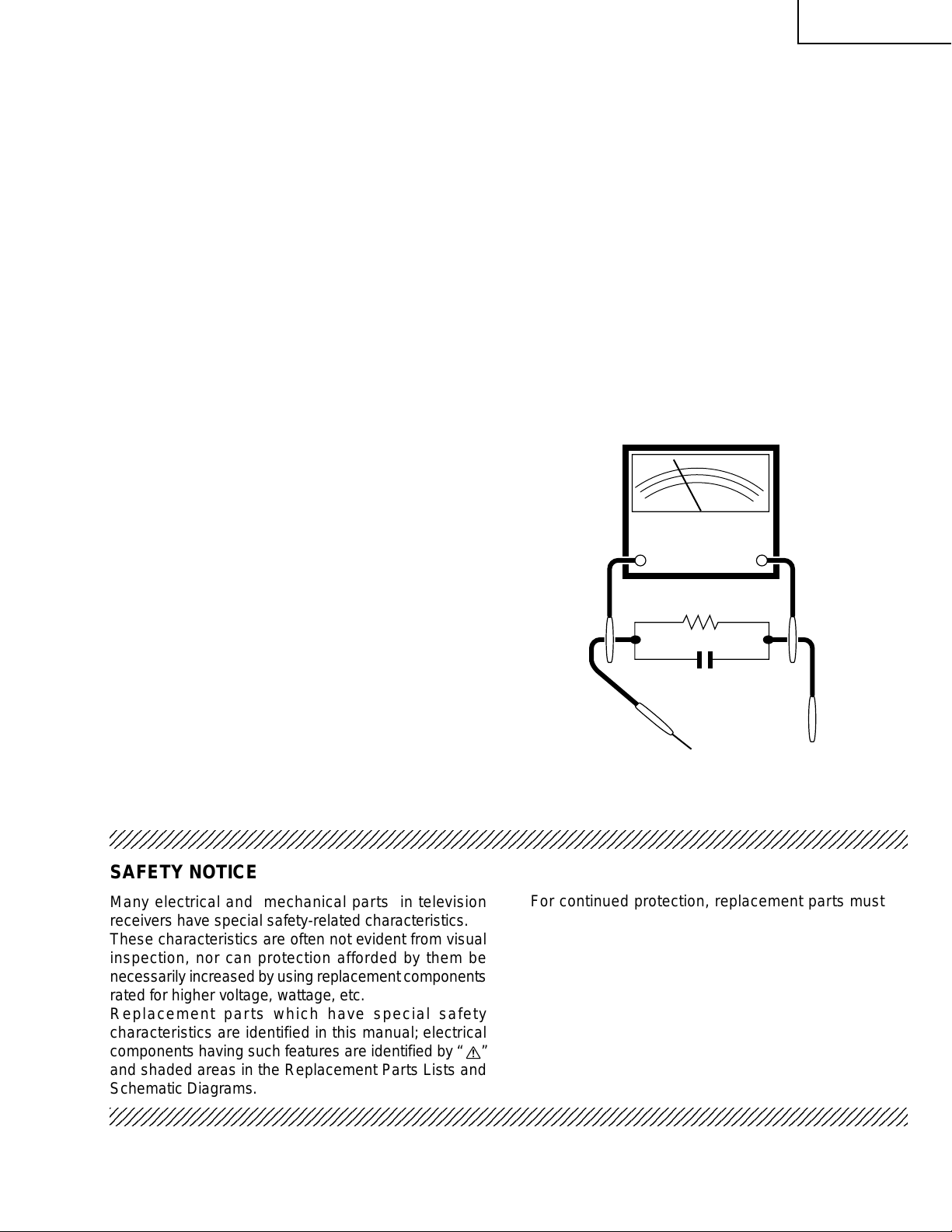
3. To be sure that no shock hazard exists, check for
leakage current in the following manner.
» Plug the AC cord directly into a 120 volt AC outlet,
(Do not use an isolation transformer for this test).
» Using to clip leads, connect a 1.5k ohm, 10 watt
resistor paralleled by a 0.15µF capacitor in series with
all exposed metal cabinet parts and a known earth
ground, such as electrical conduit or electrical ground
connected to earth ground.
» Use an AC voltmeter having with 5000 ohm per volt,
or higher, sensitivity to measure the A C v oltage drop
across the resistor.
» Connect the resistor connection to all exposed metal
parts having a return to the chassis (antenna, metal
cabinet, screw heads, knobs and control shafts,
escutcheon, etc.) and measure the AC voltage drop
across the resistor.
AII check must be repeated with the AC line cord
plug connection reversed. (If necessary, a nonpolarized adapter plug must be used only for the
purpose of completing these check.)
Any current measured must not exceed 0.5 milliamp.
Any measurements not within the limits outlined
above are indicative of a potential shock hazard and
corrective action must be taken before returning the
instrument to the customer.
AC
VOLTMETER
1.5k ohm
10W
0.15µF
TEST PROBE
TO EXPOSED
METAL PARTS
234567890123456789012345678901212345678901234567890123456789012123456789012345678901234567890121
CONNECT TO
KNOWN EARTH
GROUND
SAFETY NOTICE
Many electrical and mechanical parts in television
receivers have special safety-related characteristics.
These characteristics are often not evident from visual
inspection, nor can protection afforded by them be
necessarily increased by using replacement components
rated for higher voltage, wattage, etc.
Replacement parts which have special safety
characteristics are identified in this manual; electrical
components having such features are identified by “ å”
and shaded areas in the Replacement Parts Lists and
Schematic Diagrams.
234567890123456789012345678901212345678901234567890123456789012123456789012345678901234567890121
For continued protection, replacement parts must be
identical to those used in the original circuit. The use of
a substitute replacement parts which do not have the
same safety characteristics as the factory recommended
replacement parts shown in this service manual, may
create shock, fire, X-radiation or other hazards.
3
Page 4
27DV-S100
27DV-CS10
PRECAUTIONS A PRENDRE LORS DE LA REPARATION
Ë
Ne peut effectuer la réparation qu’ un technicien spécialisé qui s’est parfaitement
accoutumé à toute vérification de sécurité et aux conseils suivants.
AVERTISSEMENT
1. N’entreprendre aucune modification de tout circuit.
C’est dangereux.
2. Débrancher le récepteur avant toute réparation.
3. Les déversoirs thermiques à semi-conducteurs
peuvent présenter un danger de choc électrique
lorsque le réceqteur est en marche.
4. Le châssis de ce récepteur a deux systèmes de mise
à la terre qui sont séparés par un matériau isolant.
Le système de mise à la terre non-isolée (chaud) est
pour le circuit du régulateur de tension +B et le circuit
de sortie horizontale. Le système de mise à la terre
isolé est pour les basses tensions C. C . +B et le circuit
secondaire du transformateur de haute tension.
PRECAUTION: POUR LA
PROTECTION CONTINUE
CONTRE LES RISQUES
6.3A 125V
D'INCENDIE, REMPLACERLE
FUSIBLEPAR UN FUSIBLE DE
MEME TYPE 6.3-125V .
REPARATION DU SYSTEME A HAUTE
TENSION ET DU TUBE-IMAGE
Lors de la réparation de ce systéme, supprimer la
charge statique en branchant une résistance de 10
k en série a vec un fil isolé (comme une sonde
d’essai) entre la mise à la terre du tube-image et le
fil d’anodel. (Le corden d’alimentation doit être retiré
de la prise murale.)
1. Il est à noter que le tube-image de ce récepteur est
intégralement protégé contre l’implosion.
2. Par mesure de sécurité, changer le tube-image pour
un tube du même numéro de type.
3. Ne pas lever le tube-image par son col.
4. Ne manipuler le tube-image qu’en porant des lunettes
incassables et qu’après avoir déchargé totalement
la haute tension.
LIMITES DES RADIATIONS X ET DE LA
HAUTE TENSION
1. Tout le personnel réparateur doit être instruit des
instructions et procédés relatifs aux radiations X.
Le tube-image, seule source de rayons X dons les
téleviseurs transistorisés, n’émet pour tant pas de
rayons mesur ables si la haute tension est mainten ue
à un niveau préconisé dans la section “Vérification
de la haute tension”.
C’est seulement quand la haute tension est excessiv e
que les rayons X peuv ent entrer dans l’enveloppe du
tube-image y compris le conducteur de verre. Il est
important de maintenir la haute tension en-dessous
du niveau spécifié.
2. Il est essentiel que le réparateur ait sous la main un
voltmètre à haute tension qui doit être périodiquement
étalonné.
3. La haute tension doit toujours être maintenue à la
valeur de régime-et pas plus haute. L’opér ation à des
tensions plus élevées peut entraîner une panne du
tube-image ou du circuit à haute tension et, dans
certaines conditions, peut entraîner une radiation
dépassant les niveaux préscrits.
4. Quand le régulateur à haute tension fonctionne
correctement, il n’y a aucun problème de radiation X.
Chaque fois qu’un châssis couleurs est réparé, la
luminosité doit être examinée bout en contrôlant la
haute tension à l’aide d’un voltmètre pour s’assurer
que la haute tension ne dépasse pas la valeur
spécifiée et qu’elle soit correctement réglée.
5. Ne pas utiliser un tube-image autre que celui spécifié
et ne pas effectuer de modifications déconseillées
du circuit à haute tension.
6. Lors de la recherche des pannes et des mesures
d’essai sur un récepteur qui présente une haute
tension excessive, éviter de s’approcher inutilement
du récepteur.
Ne pas faire fonctionner le récepteur plus longtemps
que nécessaire pour localiser la cause de la tension
excessive.
4
Page 5
27DV-S100
2
2
27DV-CS10
PRECAUTIONS A PRENDRE LORS DE LA REPARATION
(Suite)
VERIFICATIONS CONTRE L’INCEN-DIE ET
LE CHOC ELECTRIQUE
Avant de rendre le récepteur à l’utilisateur, effectuer
les vérifications suivantes.
1. Inspecter tous les faisceaux de câbles pour s’assurer
que les fils ne soient pas pincés ou qu’un outil ne soit
pas placé entre le châssis et les autres pièces
métalliques du récepteur.
2. Inspecter tous les dispositifs de protection comme
les boutons de commande non-métalliques, les
isolants, le dos du coffret, les couvercles ou blindages
de réglage et de compar timent, les réseaux de
résistance-capacité, les isolateurs mécaniques, etc.
3. S’assurer qu’il n’y ait pas de danger d’électrocution
en vérifiant la fuite de courant, de la facon suivante:
» Brancher le cordon d’alimentation directem-ent à une
prise de courant de 120V. (Ne pas utiliser de
transformateur d’isolation pour cet essai).
» A l’aide de deux fils à pinces, brancher une résistance
de 1,5 k 10 w atts en parallèle avec un condensateur
de 0,15µF en série avec toutes les pièces métalliques
exposées du coffret et une terre connue comme une
conduite électrique ou une prise de terre branchée à
la terre.
» Utiliser un voltmètre CA d’une sensibilité d’au moins
5000 /V pour mesurer la chute de tension en tr avers
de la résistance.
» Toucher avec la sonde d’essai les pièces métalliques
exposées qui présentent une voie de retour au
châssis (antenne, coffret métallique, tête des vis,
arbres de commande et des boutons, écusson, etc.)
et mesurer la chute de tension CA en-travers de la
résistance.
Toutes les vérifications doivent être refaites après
avoir inversé la fiche du cordon d’alimentation. (Si
nécessaire, une prise d’adpatation non polarisée peut
être utilisée dans le but de terminer ces vérifications.)
Tous les courants mesurés ne doivent pas dépasser
0,5 mA.
Dans le cas contraire, il y a une possibilité de choc
électrique qui doit être supprimée avant de rendre le
récepteur au client.
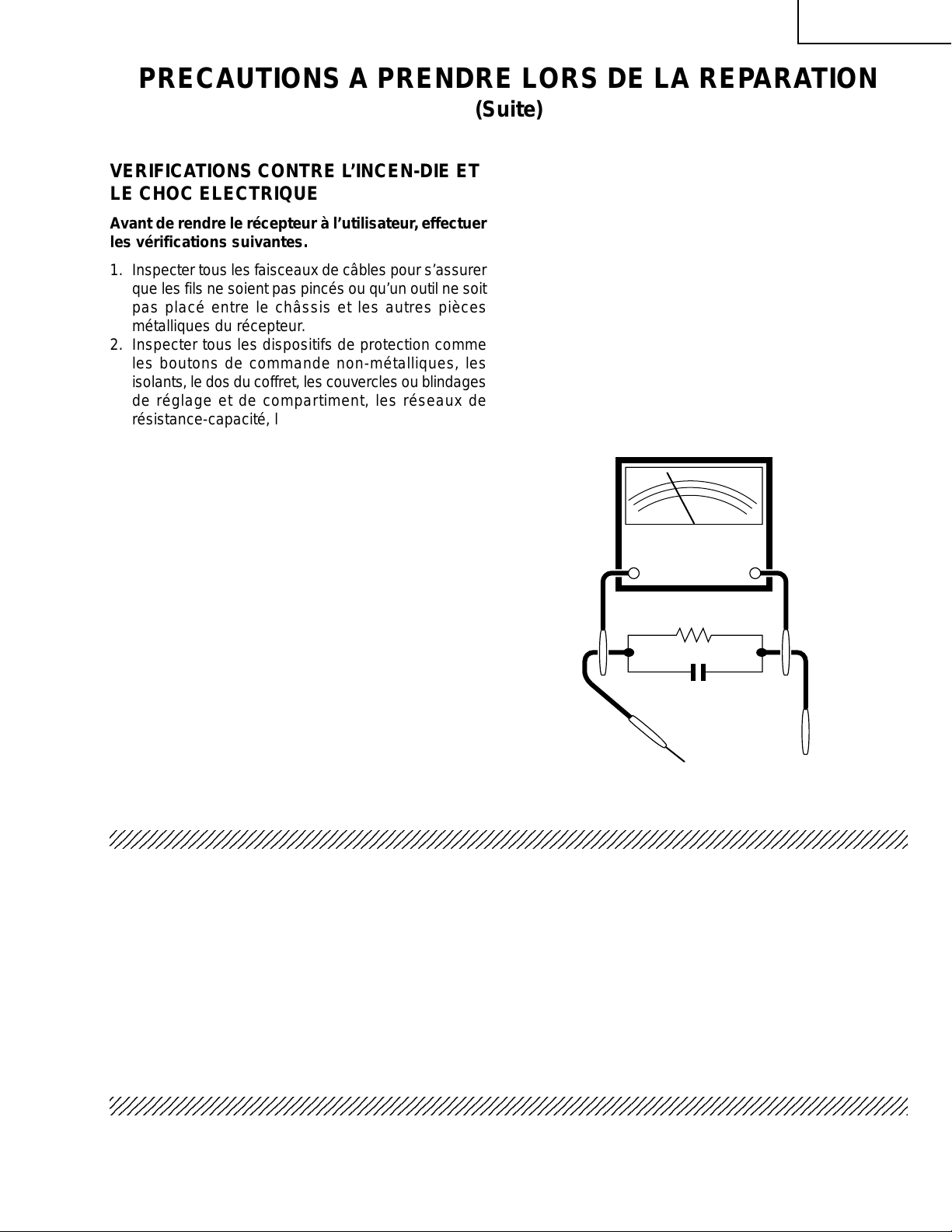
Voltmètre CA
1.5k ohm
10W
0.15µF
SONDE D'ESSAI
AUX PIECES
METALLIQUES
EXPOSEES
234567890123456789012345678901212345678901234567890123456789012123456789012345678901234567890121
BRANCHER A UNE
TERRE CONNUE
AVIS POUR LA SECURITE
De nombreuses pièces, électriques et mécaniques, dans
les téléviseurs présentent des caractéristiques spéciales
relatives à la sécurité, qui ne sont souvent pas évidentes
à vue. Le degré de protection ne peut pas être
nécessairement augmentée en utilisant des pièces de
remplacement étalonnées pour haute tension,
puissance, etc.
Les pièces de remplacement qui présentent ces
caractéristiques sont identifiées dans ce manuel; les
pièces électriques qui présentent ces particularités sont
234567890123456789012345678901212345678901234567890123456789012123456789012345678901234567890121
identifiées par la marque “ å “ et hachurées dans la
liste des pièces de remplacement et les diagrammes
schématiques.
Pour assurer la protection, ces pièces doivent être
identiques à celles utilisées dans le circuit d’origine.
L’utilisation de pièces qui n’ont pas les mêmes
caractéristiques que les pièces recommandées par
l’usine, indiquées dans ce manuel, peut provoquer des
électrocutions, incendies, radiations X ou autres
accidents.
5
Page 6
27DV-S100
27DV-CS10
SAFETY PRECAUTIONS
Precaution to be taken when replacing and servicing
the Laser Pickup.
The product is a Class 1 Laser Product.
However Laser component is capable of emitting
radiation exceeding the limit for Class 1. It is important
that following precautions are observed during servicing
to protect your eyes against e xposure to the laser beam.
1. When the cabinet is removed, interlock is defeated
(if equipped), the power is turned on without a disk
in position, Do not look into the pickup lens.
2. The laser power output of the pickup unit and
replacement service par ts are all factory pre-set
before shipment.
Do not attempt to re-adjust the laser pickup unit
during replacement or servicing.
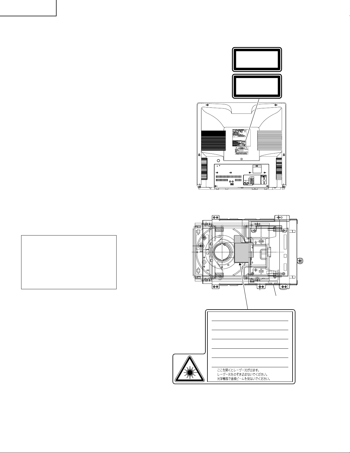
PRODUIT LASER
DE CLASSE 1
CLASS 1
LASER PRODUCT
3. Under no circumstances stare into the pickup lens
at any time.
4. Caution-Use of controls or adjustment or
performance of procedures other than those
specified herein may result in hazardous radiation
exposure.
» LASER SPECIFICATIONS
Laser Diode Properties
Material : AIGalnP
Wave length
D VD: 645~660nm
CD : 770~810nm
Emission Duration : Continuous
Laser output : Max. 0.6 mW
(Top View)
CAUTION-WHEN OPEN. DO NOT STARE INTO BEAM
OR VIEW DIRECTLY WITH OPTICAL INSTRUMENTS.
VARNONG-NÄR DENNA DEL ÄR ÖPPNAD. STIRRA EJ IN I STRÅLEN
OCH BETRAKTA EJ STRÅLEN MED OPTISKA INSTRUMENT.
ADVARSEL-VED ÅBNING. SE IKKE IND I
STRÅLEN-HELLER IKKE MED OPTISKE INSTRUMENTER.
VARO! AVATTAESSA OLET ALTTIINA. ÄLÄ TUIJOTA
SÄTEESEEN ÄLÄKÄ KATSO SITÄ OPTISEN LAITTEEN LÄPI.
VARNING-NÄR DENNA DEL ÄR ÖPPNAD. STIRRA EJ IN I STRÅLEN
OCH BETRAKTA EJ STRÅLEN GENOM OPTISKT INSTRUMENT.
ADVARSE-NÅR DEKSEL ÅPNES. STIRR IKKE INN I STRÅLEN
ELLER SE DIREKTE MED OPTISKE INSTRUMENTER.
(Back of product)
DVD Unit
NOTE:
Laser beam is emitted when this is open.
Do not stare into the beam.
Do not view the beam through any optical instrument,
either.
6
Page 7

ELECTRICAL SPECIFICATIONS
TV SECTION
POWER INPUT: 120 V AC 60 Hz
POWER RATING: 165 W
PICTURE SIZE
Width: 37.8 cm
Height: 38.7 cm
Depth: 37.5 cm
CONVERGENCE: Magnetic
SWEEP DEFLECTION: Magnetic
FOCUS: Hi-Bi-Potential Electrostatic
INTERMEDIATE FREQUENCIES
Picture IF Carrier Frequency: 45.75 MHz
Sound IF Carrier Frequency: 41.25 MHz
Color Sub-Carrier Frequency: 42.17 MHz (Nominal)
AUDIO POWER OUTPUT RATING: 3 W + 3 W (at 10% Distortion)
SPEAKER
Size: 8 cm (3-1")
Voice Coil Impedance: 16 ohm at 400 Hz
VHF/UHF ANTENNA INPUT IMPEDANCE: 75 ohm unbalanced
TUNING RANGES
VHF-Channels: 2 thru 13
UHF -Channels: 14 thru 69
CATV Channels: 1,14 thru 125 (EIA, Channel Plan)
27DV-S100
27DV-CS10
VCR SECTION
Video Recording System: Rotary Two-Head Helical Scanning
Number of Video Heads: 4 pcs.
Video Signal Standard: NTSC Color System
Maximum Recording Time: (SP)120 min (with T-120)
DVD SECTION
Playback-compatible discs: DVD (regional code "1"/"ALL"), Video CD (NTSC),
Operating Temperature: 5°C to 40°C (41°F to 104°F)
Storage Temperature: -20°C to 60°C (-4°F to 140°F)
Format: VHS Standard
Tape Width: 12.7mm (1/2inch)
Tape Speed: (SP)33.35mm/sec (1.31 i.p.s)
(LP)16.68mm/sec (0.66 i.p.s)
Play back only
(EP)11.12 mm/sec (0.44 i.p.s)
(EP)360 min (with T-120)
Video Input: 0.5 to 2.0 Vp-p, 75 ohm unbalanced
Audio Input: -8 dB, 47k ohm unbalanced (0 dB-0.775 Vrms)
CD, DA, MP3, Music CD
Signal system: NTSC
Specifications are subject to change without prior notice.
7
Page 8
27DV-S100
27DV-CS10
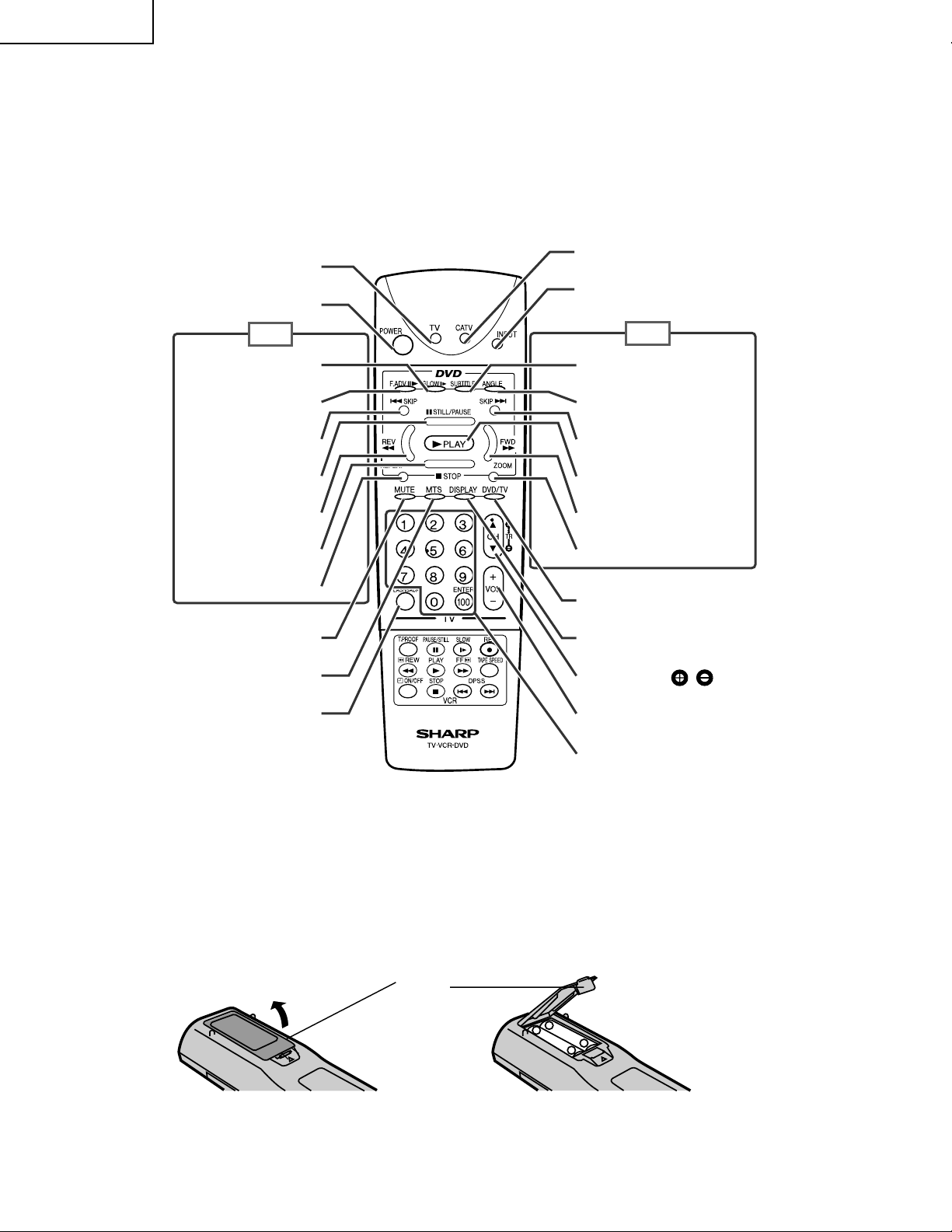
LOCATION OF USER'S CONTROL
Front (TV/VCR controls)
Cassette
compartment
POWER button
»
REC button
ÈREW (rewind) button
VOL + / – (UP/DOWN) buttons
' / " (UP/DOWN) buttons
CH
Front (DVD controls)
VCR mode indicator
|PLAY button
Ë
STOP/ EJECT button
TAMPER PROOF indicator
PROGRAM TIMER indicator
REC indicator
POWER/WAKE-UP TIMER indicator
è
FF (fast forward) button
Sensor area for Remote Control
DVD mode indicator
OPEN-CLOSE button
|È
SKIP/REV (reverse) button
|PLAY button
|
SKIP/FWD (forward) è
VIDEO / L-AUDIO-R terminals
Ë Insert the headphones (not supplied) into the headphone jack to listen to audio.
button
(Inside the cover)
PHONES (Headphone jack)
Ë
STOP button
8
Disc tray
Page 9
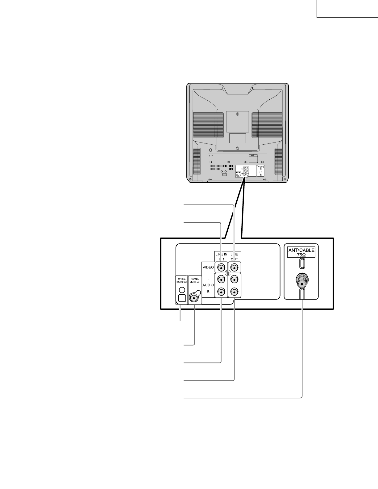
Rear
27DV-S100
27DV-CS10
LOCATION OF USER'S CONTROL (Continued)
Video output terminal
Video input terminal
DVD OPTICAL DIGITAL output terminal
DVD COAXIAL DIGITAL output terminal
Audio input terminals
Audio output terminals
ANT/CABLE terminal (75Ω)
9
Page 10
27DV-S100
27DV-CS10
Remote Control Unit (Cover closed)
LOCATION OF USER'S CONTROL (Continued)
TV
POWER
DVD
SLOW
F.ADV
SKIP (REV)
STILL/PAUSE
REV (reverse)
STOP
REPEAT
MUTE
MTS
CATV
INPUT
DVD
SUBTITLE
ANGLE
SKIP (FWD)
PLAY
FWD (forward)
ZOOM
DVD/TV
DISPLAY
CH '/", TR /
FLASHBACK
Ë Using Your Remote Control With Your unit
After installing the batteries, press TV to switch to the TV mode. (If you can change the channel of the TV by
pressing CH '/" or CHANNEL SELECT buttons,you are in TV mode.)
+
/
VOL
CHANNEL SELECT buttons
–
Loading the Batteries
Ë Before using the unit, prepare the Remote Control.
To use the Remote Control, insert batteries first.
Insert the batteries
Battery
Pull up
• With your thumbnail, pull up the slit as indicated by the arrow to remove the back cover. Insert two batteries
(size “AA”). Be sure to match the battery
Cover
–
+
±/— terminals with the ±/— marks inside the compartment.
+
–
10
Page 11
LOCATION OF USER'S CONTROL (Continued)
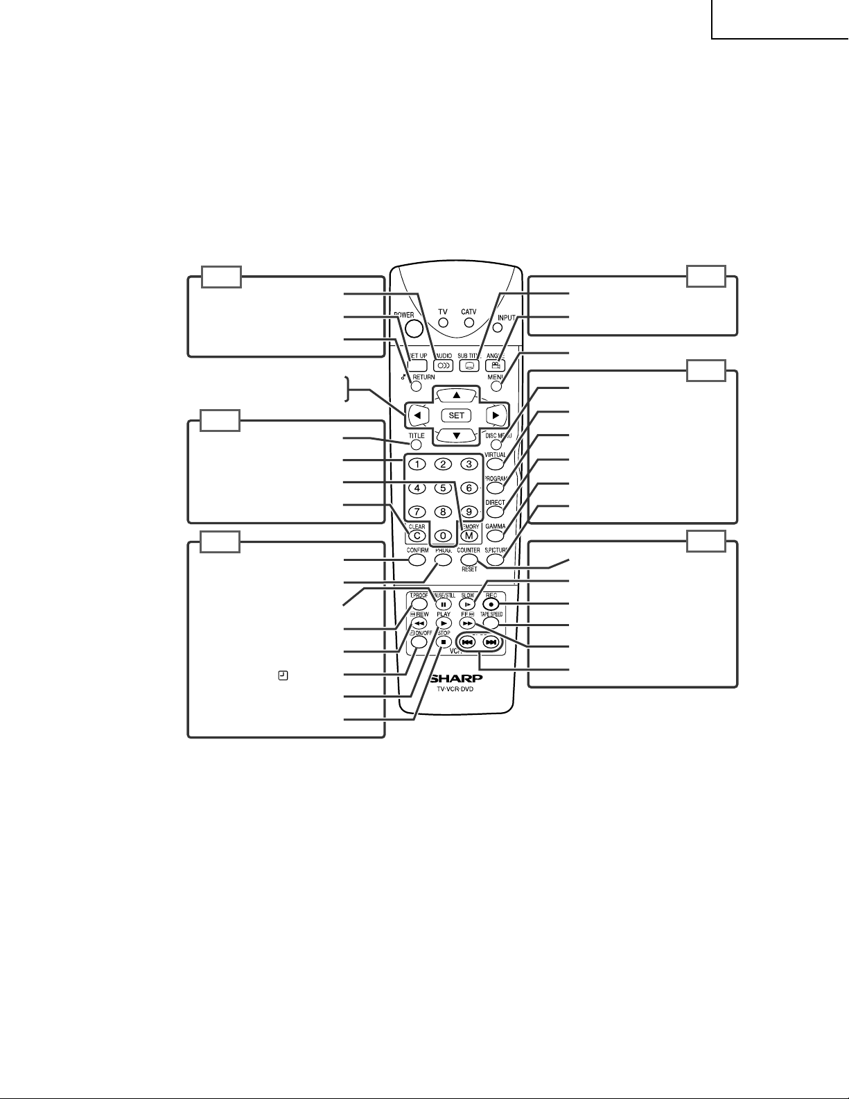
Remote Control Unit (Cover open)
27DV-S100
27DV-CS10
DVD
RETURN
CURSOR
DVD
NUMBER buttons
MEMORY
VCR
CONFIRM
PAUSE/STILL
T.PROOF
REW (rewind)
AUDIO
SET UP
SET
TITLE
CLEAR
PROG.
ON/OFF
PLAY
STOP
DVD
SUBTITLE
ANGLE
MENU
DVD
DISC MENU
VIRTUAL
PROGRAM
DIRECT
GAMMA
S.PICTURE
VCR
COUNTER RESET
SLOW
REC (record)
TAPE SPEED
FF (fast forward)
DPSS
11
Page 12
27DV-S100
27DV-CS10
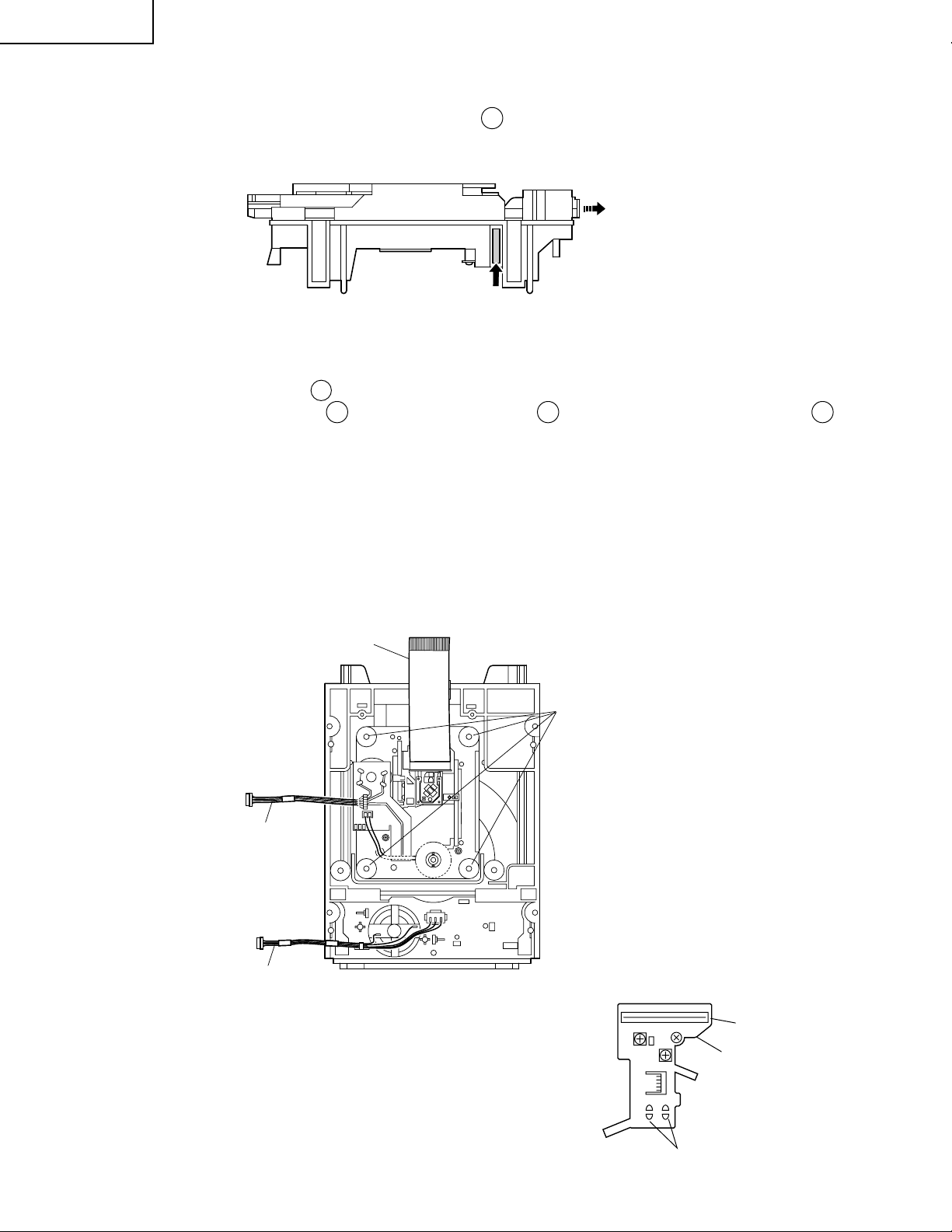
DISASSEMBLY AND REASSEMBLY
1. Remove the 16 rear cover fixing screws and detach the rear cover.
2. Take out the anode cap, CRT PWB, connectors OO, K and M, coating earth, speaker connectors SE, connector
DC and others.
3. Remove the 2 main chassis fixing screws and take out the main chassis.
4. Remove the 5 fixing screws from the sub-chassis f or the VCR power/deflection PWB and detach this sub-chassis.
5. Remove the 5 VCR shielding case fixing screws and detach the shielding case.
6. Remove the 4 cassette housing fixing screws and detach the cassette housing.
1
2
OO
OO
DC
DC
SE
K
M
M
3
4
5
6
12
Page 13
27DV-S100
27DV-CS10
7. Remove the 2 mechanism chassis bracket fixing screws and the head amplifier shielding case fixing screw.
8. Remove the 3 mechanism chassis fixing screws and detach the mechanism chassis from the main PWB.
9. Remove the 2 DVD mechanism unit reinforcement fixing screws and detach this reinforcement.
10.Remove the 4 DVD mechanism unit fixing screws and detach the DVD mechanism unit.
11.Remove the 1 main PWB fixing screws and detach the main PWB.
12.Remove the 1 TV signal PWB fixing screw and detach the TV signal PWB.
13.Remove the 2 TV power PWB fixing screws and detach the TV power PWB.
7
8
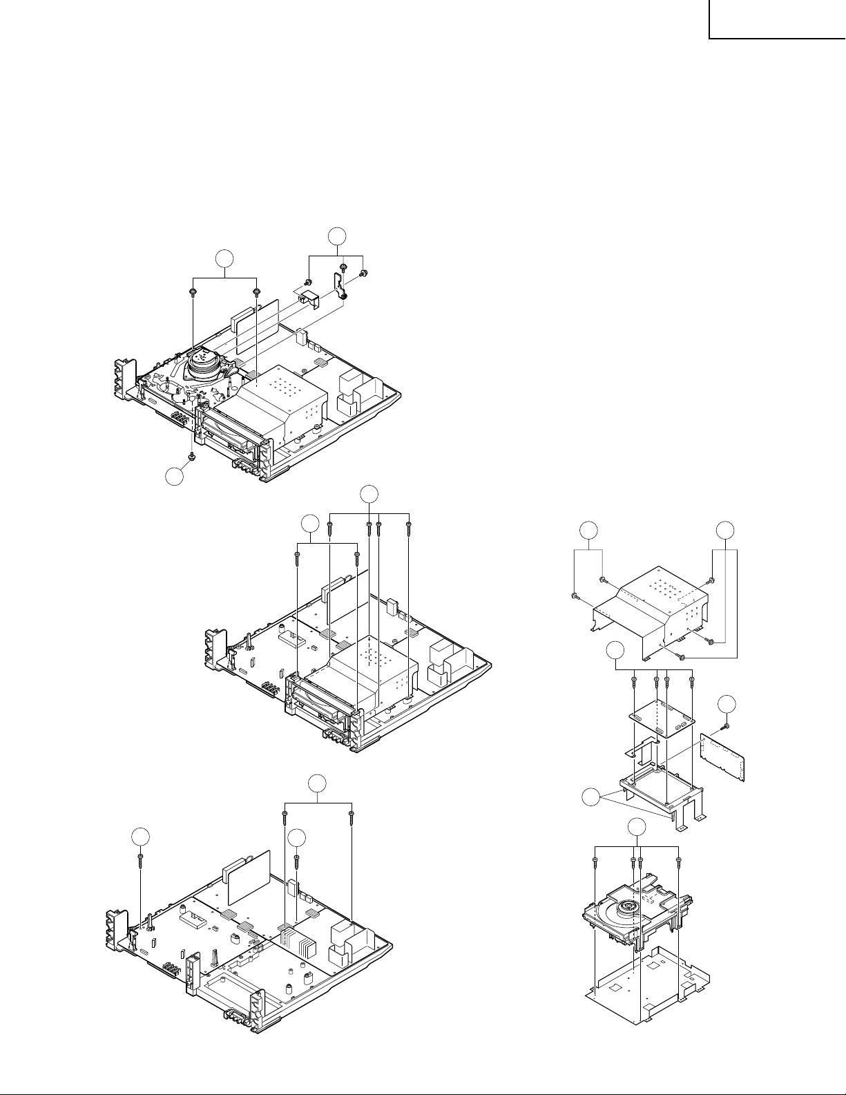
» DVD section
14.Remove the 5 DVD shielding case fixing screws and
detach the DVD shielding case.
15.Undo the 4 hooks from the chassis for the DVD main
and sub PWBs, and detach this chassis.
16.Remove the 4 DVD main PWB fixing screws and
detach the DVD main PWB.
17.Remove the DVD sub PWB fixing scre w , undo the hook
and detach the DVD sub PWB.
18.Finally remove the 4 DVD mechanism fixing screws
and detach the DVD mechanism.
8
10
9
14 14
11
12
16
17
13
15
18
13
Page 14
27DV-S100
27DV-CS10
REPLACEMENT OF MAIN PARTS
<Take out disk>
1. Remove the mechanism with angle from the set (refer to 17 on PARTS LIST (See page 183)).
2. It is in such cases as the thin driver, and it is pushed in slowly, and a tra y is dra wn in the arrow direction the slide
rack on the left of the base chassis.
3. Take out disk.
Front Side
<Disassembling and assembling the mechanism chassis>
1. After setting the mechanism chassis to the angle state, ground it to prevent the electrostatic discharge damage
of the pickup.
2. Remove the DVD shield (lower) 5 (refer to the illustration on PARTS LIST (See page 183)).
3. Remove the DVD main PWB unit 35 , and loosen the 4 screws 56 to remove the DVD main PWB unit 35 .
(Pickup relay FFC isn’t removed.) (refer to the illustration on PARTS LIST (See page 183))
4. Remove screws fixing the base chassis (located at the back right and at front left when facing the set).
5. With the pickup FFC connected, turn over the base chassis and short (solder) two short lands on the pickup
interface PWB in order to prevent the electrostatic discharge damage of the pickup.
6. Remove the pickup FFC from the main PWB.
7. Remove the pickup FFC from the pickup interface PWB.
8. Remove the traverse mounting screws to remove the traverse chassis ass’y.
Note: After assembly and wiring, remove the solder joint of the short land. If short-circuited, a disk is not played
back.
Pickup FFC
Sled Motor Lead Wire
Loading Motor Lead Wire
<Replacing the pickup and the spindle motor>
Since the pickup optical axis and turntable inclination of DVD are adjusted
with higher accuracy than of CD/MD, make a replacement as a mechanism
service chassis ass’y (refer to Parts List).
Traverse Fixing Screw
Pickup FFC
Pickup interface PWB
14
Short Land
Page 15
27DV-S100
BA
XB
XB
SE
ZA
XC
ZA
OC
DB
AR
DB
DD
DA
DC
DF
27DV-CS10
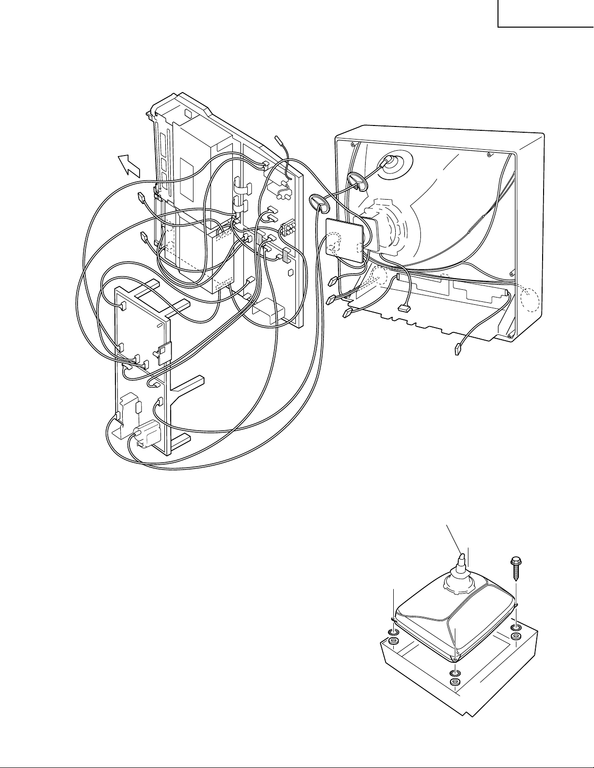
For servicing the TV’s component units, undo the lead dressing holders and place the main chassis upright as shown
below. Connect necessary leads for quick servicing.
OO
FRONT
SC
SA
AR
SA
DC
AR
SE
EB
AR
ZA
ZA
SB
OC
OC
DB
DB
DE
ZA
ZA
DF
DF
DC
DC
DB
DB
DA
DA
DD
DD
WA
SB
DA
GBN
XB
XB
DF
BA
BA
SE
SE
XB
XB
EB
M
XC
XC
GA
OR
XC
GBN
PU
N(H)
M
DC
SE
DC
K
OO
SC
DD
OC
WA
BA
GA
Remove the four screws from the cathode ray tube, and detach
the cathode ray tube (weighing 35 kg or so).
» The cathode ray tube has a high-tension static charge and a
high vacuum. Handle it with enough care on the following
occasions.
N
K
For disposal of the cathode ray tube
1) The high-voltage electrode, which is covered with the anode
cap atop the cathode ray tube, may have a high-tension static
charge. Before detaching the anode cap, be sure to get this
electrode fully discharged.
2) The cathode ray tube has a high vacuum inside. Crack the tip
of the air vent on the neck socket of the cathode ray tube in
order to get the tube out of vacuum.
OO
Get the air vent tip cracked to let in air.
~
~
~
~
15
Page 16

27DV-S100
27DV-CS10
INSTALLATION AND SERVICE INSTRUCTIONS
Note: (1) When performing any adjustments to resistor controls and transformers use non-metallic scre wdriver
or TV alignment tools.
(2) Before performing adjustment, TV set must be on at least 15 minutes.
CIRCUIT PROTECTION
The receiver is protected by a 6.3A fuse (F701), mounted
on PWB-A, wired into one side of the AC line input.
X-RADIATION PROTECTOR CIRCUIT
TEST
After service has been performed on the horizontal
deflection system, high voltage system, or +B system,
test the X-Radiation protector circuit to ascertain proper
operation as follows:
1. Apply 120V AC using a variac transformer for accurate
input voltage.
2. Allow for warm up and using the remote controller,
set the brightness level and contrast level to
maximum.
3. Check the voltage of test point TP653. (It’s voltage
should be about 11.1V DC.)
4. Apply external 14.5V DC at TP653 by using an
external DC supply . The increased v oltage will cause
the horizontal oscillator to stop and the TV to shut
off.
5. To re-star t the oscillator, remove the external DC
power supply and short together TP651 and TP652.
Once the TV set operates normally again, remove
the short between TP651 and TP652.
HIGH V OL T AGE CHECK
High voltage is not adjustable b ut must be checked
to verify that the receiver is operating within safe
and efficient design limitations as specified checks
should be as follows:
1. Connect an accurate high voltage meter between
ground and anode of Picture tube.
2. Operate receiver for at least 15 minutes at 120V AC
line voltage, with strong air signal or properly tuned
in test signal.
3. Set to Ser vice mode on, “Mute” and bus data 1(Ymute on).
4. The voltage should be approximately 29.2kV (at zero
beam). If a correct reading cannot be obtained, chec k
circuitry for malfunctioning components.
After the voltage test, “Mute” and b us data “0” (Y-mute
off).
16
Page 17
27DV-S100
27DV-CS10
The R-series SHARP TV/VCR COMBINATION have most of the analog setup adjustments eliminated. Coil and
variable resistor adjustments are now performed digitally by using the remote controller or set’s volume and
channel change function buttons.
Note: There are still a few analog adjustments in the R-series such as 120V adjust, focus, master screen
voltage and coils in the picture I/F detector circuit.
Follow the steps below , whenever service adjustment is required. See “T ab le-B” to determine, if service
adjustments are required.
1. Service mode
Before putting unit into the service mode, check that
customer adjustments are in the normal mode, use
the reset function in the video adjust menu to ensure
customer controls are in their proper (reset) position.
To enter the service mode
Plug in a television set, during push S2507 (CH-up).
When successfuly entered, the service mode will be
displayed as shown in Figure A.
To exit service mode
Turn off the power or unplug the set.
2. Adjustment Item selection
Once in the service mode, press the channel up or
channel down button on the remote controller or at
the set (Table-A). Select the item y ou wish to adjust.
3. Data number selection
Press the volume up or down button to adjust the
data number in the upper right hand side of the
screen.
Figure A.
17
Page 18
27DV-S100
27DV-CS10
ITEM
SUB COTRAST(*1) PICTURE 20 00 - 31 Adjustment is required of each set.
TINT (*1) TINT 30 00 - 47 Adjustment is required of each set.
SUB COLOR (*1) COLOR 18 00 - 31 Adjustment is required of each set.
BRIGHTNESS (*1) BRIGHT 55 00 - 95 Adjustment is required of each set.
SHARPNESS SHARP 15 00 - 47 Fix at "8"
V-POSITION (*1) V POSITION 95 00-127 Adjustment is required of each set.
H-POSITION (*1) H POSITION 17 00 - 31 Adjustment is required of each set.
R CUT-OFF (*1) R CUT-OFF 64 00-255 Adjustment is required of each set.
G CUT-OFF (*1) G CUT-OFF 64 00-255 Adjustment is required of each set.
B CUT-OFF (*1) B CUT-OFF 64 00-255 Adjustment is required of each set.
G GAIN (*1) G GAIN 64 00-127 Adjustment is required of each set.
B GAIN (*1) B GAIN 64 00-127 Adjustment is required of each set.
Y-γ CURVE Y-γ CURVE 00 00 - 03 Fix at "03"
VSM PHASE VSM PHASE 01 00 - 03 Fix at "02"
APACON PEAK f0 APA PEAK f0 01 00 - 07 Fix at "01"
DC RESTRATION RATE DC REST 21 00 - 63 Fix at "07"
DC RESTRATION LIMIT DC REST LMT 00 00 - 03 Fix at "02"
BLACK STRETCH POINT BLK STRETCH 03 00 - 07 Fix at "00"
APL VS BPS APL VS BPS 01 00 - 03 Fix at "01"
B.L.C B.L.C 01 00 - 01 Fix at "00"
DYNAMIC ABL POINT DY ABL POINT 04 00 - 07 Fix at "06"
DYNAMIC ABL GAIN DY ABL GAIN 04 00 - 07 Fix at "03"
ABL POINT ABL POINT 03 00 - 07 Fix at "07"
ABL GAIN ABL GAIN 03 00 - 07 Fix at "04"
Y-DL Y-DL 01 00 - 01 Fix at "01"
TOF-Q TOF-Q 04 00 - 07 Fix at "04"
VSM GAIN VSM GAIN 01 00 - 03 Fix at "02"
OSD SL OSD SL 00 00 - 01 Fix at "00"
C-DECODE C-DECODE 161 00-255 Fix at "153"
DVD BR-OFF DVD BR-OFF 30 30 - 70 Fix at "50"
PICTURE HEIGHT V AMP 22 00-127 Adjustment is required of each set.
V-LINEARITY V-LINEARITY 22 00 - 31 Adjustment is required of each set.
V-S CORRECTION V-S CORRECT 40 00 - 63 Fix at "47"
PICTURE WIDTH H AMP 30 00 - 63 Adjustment is required of each set.
E-W PARABOLA E-W PARABOLA 19 00 - 63 Adjustment is required of each set.
E-W CORNER E-W CORNER 18 00 - 31 Adjustment is required of each set.
TRAPEZIUM TRAPEZIUM 55 00-127 Adjustment is required of each set.
AGC AGC 01 00 - 01 Fix at "01"
Y-MUTE MUTE 00 00 - 02 00=NORMAL, 01=NO-Y, 02=NO-VERTICAL
ENERGY SAVE ENERGY SAVE 21 00 - 63 Fix at "21"
TEXT BOX TEXT BOX 8 00 - 31 Adjustment is required of each set.
TEXT PICTURE TEXT PICTURE 20 00 - 80 Fix at "20"
CCD LEVEL CCD LEVEL 04 00 - 20 Fix at "10"
OPTION (VCR) OPTION (VCR) 39 00-255 Fix at "39"
OPTION (TV) OPTION (TV) 31 00-127 Fix at "127"
MTS INPUT LEVEL INPUT LEVEL 07 00 - 15 Adjustment is required of each set.
MTS VCO MTS VCO 37 00 - 63 Adjustment is required of each set.
MTS FILTER FILTER 30 00 - 63 Adjustment is required of each set.
WIDE BAND DETECT WIDE BAND 35 00 - 63 Adjustment is required of each set.
SPECTRAL DETECT SPECTRAL 22 00 - 63 Adjustment is required of each set.
H COMP H COMP 03 00 - 07 Fix at "03"
V COMP V COMP 03 00 - 07 Fix at "03"
CCD POSITION CCD POSITION 38 00 - 63 Fix at "38"
OSD DISPLAY INITIAL
RANGE SETTING DATA
(*1) Set the adjustment value to tuner input instead of the adjustment at DVD input (play).
Table-A
PART ADJUSTMENT
REPLACED NECESSARY UNNECESSARY
IC2001 X Data is stored in IC2003.
IC401 X
IC2003 X
CRT X Adjust items related to picture tube only.
The adjustment is needed to compensate for characteristics
of parts including IC401.
Initial setting values are written from IC2001. Adjust for best
results.
NOTE
Table-B
18
Page 19

Ë
SERVICE ADJUSTMENT
Screen Adjustment
1. Select a good local channel.
2. Enter the service mode and select the service
adjustment item "COLOR" and set the data value to
"0" to set the color level to minimum. You may skip
this step, if you selected a B/W picture or monoscope
pattern.
3. Select service adjustment item "MUTE" and adjust
the data value to "1", this turns off the luminance
signal (Y-mute).
4. Adjust the master screen control until raster darkens
to the point where raster is barely seen.
5. Adjust service adjustments item "R-CUT OFF" red
"G-CUT OFF" green and "B-CUT OFF" blue to obtain
a good grey scale with normal whites at low brightness
level.
6. Select the service adjustment item "MUTE" and reset
data to "0". Select service adjustment item "COLOR"
and reset data to obtain normal color level.
White Balance Adjustment
1. Select a good local channel.
2. Enter the service mode and select the service
adjustment item "COLOR" and set to "0" (minimum
color). "COLOR" does not have to be adjusted if you
selected a B/W picture or monoscope pattern.
3. Alternately adjust the service adjustment data of "G
GAIN" and "B GAIN" until a good grey scale with
normal whites is obtained.
4. Select the ser vice adjustment item "COLOR" and
adjust data to obtain normal color level.
Picture Adjustment
1. Select a good local channel.
2. Make sure the customer picture control is maximum.
3. Enter the service mode and select the service
adjustment item "PICTURE".
4. Adjust the data value to achieve normal contrast
range.
Tint Adjustment
1. Select a good local channel.
2. Set customer tint control to center of it’s range.
3. Enter the service mode and select the service
adjustment item "TINT".
4. Adjust "TINT" data value to obtain normal flesh tones.
Color Adjustment
1. Select a good local channel.
2. Make sure the customer color control is set to center
position .
3. Enter the service mode and select the service
adjustment item "COLOR".
4. Adjust "COLOR" data value to obtain normal color
level.
27DV-S100
27DV-CS10
Brightness Adjustment
1. Select a good local channel.
2. Make sure the customer brightness control is set to
center position.
3. Enter the service mode and select the service
adjustment item "BRIGHT".
4. Adjust "BRIGHT" data value to obtain normal
brightness level.
Vertical Phase Adjustment
1. Receive a good local channel.
2. Enter the service mode and select "V-POSITION".
3. Adjust data value so that picture is approximate
center.
Vertical-Size Adjustment
1. Receive a good local channel.
2. Enter the service mode and select "V-AMP".
3. While observing the top and bottom of the screen,
adjust the data value to proper vertical size.
Side Pincushion Adjustment
1. Receive a good local channel or crosshatch pattern
signal.
2. Set to standard setting mode.
3. Enter the service mode and select "E-W P ARABOLA".
4. Adjust the data so that the outer most line on the
screen be straight.
Corner Distortion Adjustment
1. Receive a good local channel or crosshatch pattern
signal.
2. Set to standard setting mode.
3. Enter the service mode and select "E-W CORNER".
4. Adjust the data so that the vertical lines should be
straight.
Trapezoidal Distortion Adjustment
1. Receive a good local channel or crosshatch pattern
signal.
2. Set to standard setting mode.
3. Enter the service mode and select "TRAPEZIUM".
4. Adjust the data so that the leftmost and rightmost
vertical lines are parallel to each other.
Horizontal Position Adjustment
1. Receive a good local channel or crosshatch pattern
signal.
2. Set to standard setting mode.
3. Enter the service mode and select "H-POSITION".
4. Adjust so that the left and right overscans are equal
to each other.
19
Page 20

27DV-S100
27DV-CS10
Horizontal Size Adjustment
1. Receive a good local channel or crosshatch pattern
signal.
2. Set to standard setting mode.
3. Enter the service mode and select "H-AMP".
4. Adjust the data to obtain the best horizontal size.
Caption Position Adjustment
(Horizontal)
1. Receive a good local channel.
2. Enter the service mode and select "TEXT BOX".
3. A black text box appears on the screen. (see Figure
B below)
4. Adjust the data value so that text box is positioned in
the center of the screen.
White Balance Adjustment of Component Signal Input
1. Feed the B/W pattern signal via the component signal
input from signal generator.
2. Set "Y-MUTE" bus data to "01" to get the Y signal
mute.
3. Select a luminance-short gun, and adjust the bus data
of "R CUT-OFF", "G CUT-OFF" and "B CUT-OFF" to
have the luminance at the white level.
4. Adjust the "G GAIN" and "B GAIN" setting to obtain
the specified white level.
Sub-brightness Adjustment of Component Signal Input
1. Feed the B/W pattern signal via the component signal
input from signal generator.
2. Make sure the customer brightness control is set to
center position.
3. Enter the service mode and select "BRIGHT".
4. Adjust the data value to obtain normal br ightness
level.
20
Page 21

Ë
MTS ADJUSTMENT
MTS Level Adjustment (for TV tuner)
1. Receive the following monaural signal. Monaural
signal: 300Hz, 245mVrms.
2. Connect the rms voltmeter to pin (39) of IC3001.
3. Enter the service mode and select "INPUT LEVEL".
4. Adjust the data so that the rms voltmeter reads 490
+10/-10mVrms.
MTS VCO Adjustment (for TV tuner)
1. Keep the unit in no-signal state.
2. Connect the frequency counter to pin (39) of IC3001.
3. Connect a capacitor (100uF, 50V) between positive
(+) side of C3005 and ground.
4. Enter the service mode and select "MTS VCO".
5. Adjust the data so that the frequency counter reads
62.94 +0.72/-0.75kHz.
Filter Adjustment (for TV tuner)
1. Feed the following stereo pilot signal to pin (14) of
IC3001. Stereo pilot signal: 9.4kHz, 600mVrms.
2. Enter the service mode and select "FILTER".
3. Adjust the data until "OK" appears in position on the
screen. Make sure the "OK" is displayed almost at
the center of the data range.
27DV-S100
27DV-CS10
Separation Adjustment (for VCR tuner)
1. Connect the rms voltmeter to pin (22) of IC3601 (or
negative (-) side of C1321).
2. Receive the following composite stereo signal 1.
Composite stereo signal: 30% modulation, left
channel only, noise reduction on, 300Hz.
3. Adjust R3601 to become the output level as the
minimum.
4. Receive the following composite stereo signal 2.
Stereo signal: 30% modulation, left channel only ,
noise reduction on, 3kHz.
5. Adjust R3612 to become the output level as the
minimum.
6. Take the above steps 1 thru 5 again for fine
adjustment.
Separation Adjustment (for TV tuner)
1. Connect the rms voltmeter to pin (39) of IC3001.
2. Receive the following composite stereo signal 1.
Composite stereo signal: 30% modulation, left
channel only, noise reduction on, 300Hz.
3. Enter the service mode and select "WIDE BAND".
4. Adjust the data until the AC voltage reading of the
rms voltmeter is minimum.
5. Receive the following composite stereo signal 2.
Stereo signal: 30% modulation, left channel ony,
noise reduction on, 3kHz.
6. Enter the service mode and select "SPECTRAL".
7. Adjust the data until the AC voltage reading of the
rms voltmeter is minimum.
8. Take the above steps 1 thru 7 again for fine
adjustment.
MTS Level Adjustment (for VCR tuner)
1. Receive the following monaural signal. Monaural
signal: 300Hz, 245mVrms.
2. Connect the rms voltmeter to pin (22) of IC3601 (or
negative (-) side of C1321).
3. Adjust R3614 to become the output level as 490
+10/-10mVrms.
21
Page 22
27DV-S100
27DV-CS10
PRECAUTIONS IN REASSEMBLING
INSTALLING THE CASSETTE HOUSING
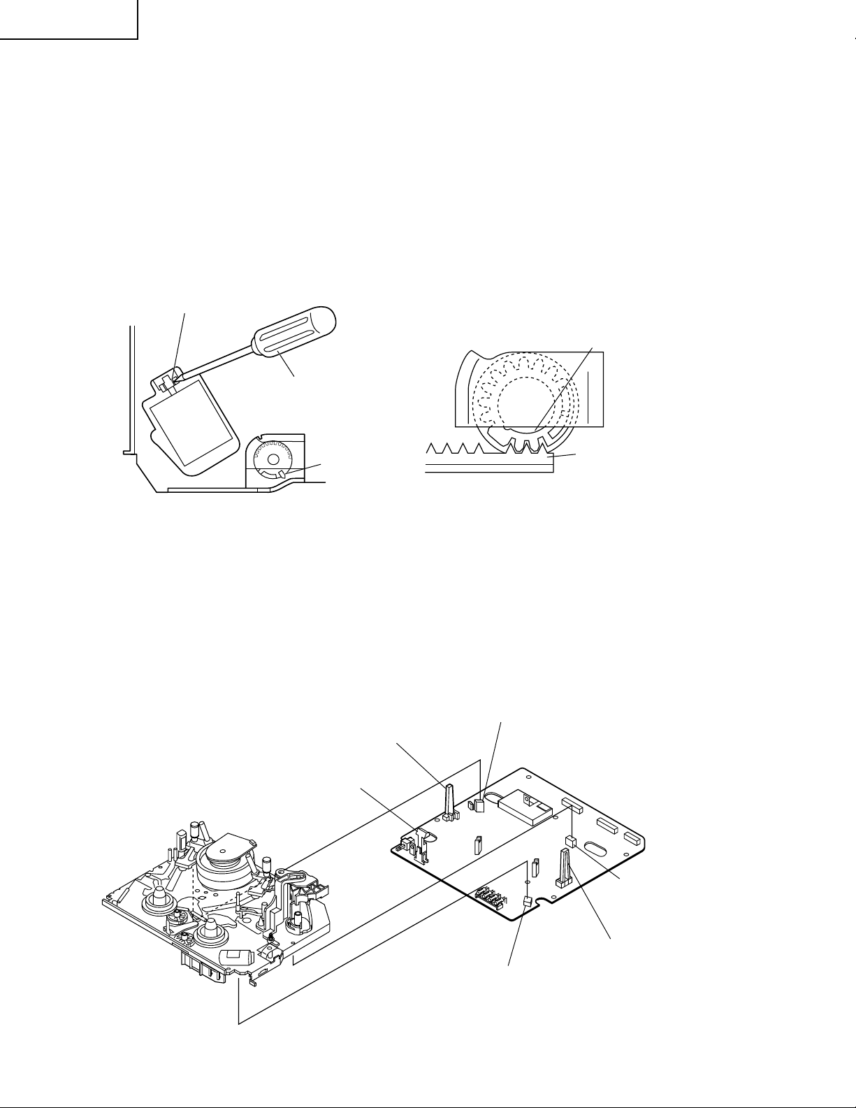
When the cassette housing is installed on the mechanism, the initial setting is essential condition.
There are two initial setting methods, namely electrical and mechanical.
1. Electrical initial setting
So as to perform initial setting of mechanism execute
the Step 1 of Installation of cassette housing. After
ascertaining the retur n to the initial setting position
(*1) install the cassette housing. (Conditions: When
mechanism and PWB have been installed)
Pulley feed gear
Screwdriver
Tint mark (*1)
Installing the mechanism on PWB
Lower vertically the mechanism, paying attention to the
mechanism edge, and install the mechanism with due
care so that the parts are not damaged. So as to fix the
mechanism to the main PWB install two housings. (Fit
the antenna cover to one of them. For other, fix the
vicinity of loading motor and solder joint side of main
PWB.) Connect again the FFC cable (AA-MH, AD-ME,
AH-MZ) between the mechanism and the main PWB.
2. Mechanical initial setting
Feed the pulley f eed gear of loading motor with screw
driver. After ascertaining the return to the initial set
position (*1) install the cassette housing in the
specified position. (This method is applied only for
the mechanism.)
Casecon
drive gear
Drive angle of
cassette housing
Parts which need particular care
When installing the mechanism chassis on the PWB
unit, take care so as to prevent deformation due to
contact of mechanism chassis with REC TIP SW.
END SENSOR
REC TIP SW
AE CONNECTOR
AD CONNECTOR
START SENSOR
AL CONNECTOR
22
Page 23
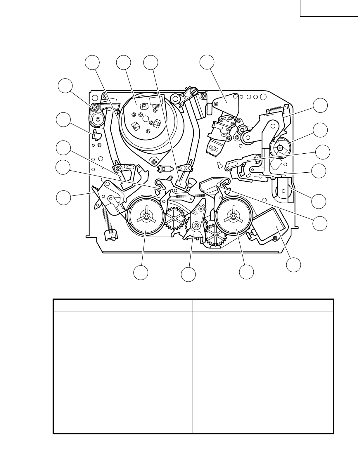
FUNCTION OF MAJOR MECHANICAL PARTS (TOP VIEW)
17
10
11
5
9
14
12
8
16
13
4
6
2
7
3
1
1815
19
27DV-S100
27DV-CS10
No. Function
1 Full erase head
2 Supply pole base ass’y
3 Tension arm ass’y
4 Idler wheel ass’y
5 Pinch drive lever ass’y
6 Supply reel disk
7 Supply main brake ass’y
8 Take-up main brake ass’y
No. Function
11 Reverse guide lever ass’y
12 Casecon drive gear
13 Take-up reel disk
14 Pinch roller lever ass’y
15 Drum ass’y
16 Loading motor
17 Drum motor
18 Take-up pole base ass’y
9 Pinch drive cam
10 A/C Head ass’y
19 Impedance roller ass’y
23
Page 24
27DV-S100
27DV-CS10
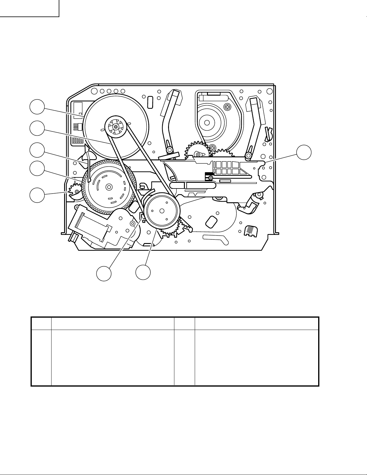
FUNCTION OF MAJOR MECHANICAL PARTS (BOTTOM VIEW)
21
22
19
20
12
23
No. Function
26
24
No. Function
12 Casecon drive gear
19 Slow brake
20 Master cam
21 Capstan D.D. motor
22 Reel belt
23 Clutch lever
24 Limiter pulley ass'y
26 Shifter
24
Page 25
27DV-S100
27DV-CS10
ADJUSTMENT, REPLACEMENT AND ASSEMBLY OF
MECHANICAL UNITS
The explanation given below relates to the on-site general service (field service) but it does not relates to the adjustment
and replacement which need high-grade equipment, jigs and skill. For example, the drum assembling, replacement
and adjustment service must be performed by the person who have finished the technical courses.
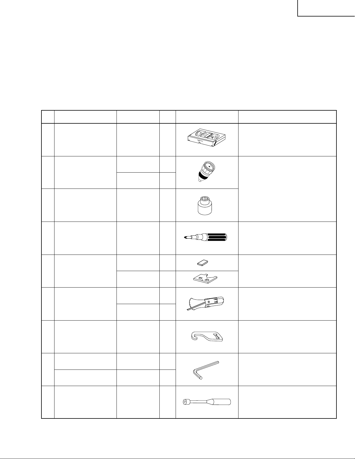
MECHANISM CONFIRMATION ADJUSTMENT JIG
So as to perform completely the mechanism adjustment prepare the following special jigs. So as to maintain the initial
performance of the machine the maintenance and check are necessary. Utmost care must be tak en so that the tape is
not damaged. If adjustment needs any jig, be sure to sue the required jig.
This cassette torque meter is used
1. Torque Cassette Meter JiGVHT-063 CZ
JiGTG0090 CM
2. Torque Gauge
JiGTG1200 CN
3. Torque Gauge Head JiGTH0006 AW
for checking and adjusting the
torque of take-up for measuring
tape back tension.
These Jigs are used for checking
and adjusting the torque of takeup and supply reel disks.
4. Torque Driver JiGTD1200 CB
Master Plane Jig and JiGRH0002 BR
5. Reel Disk Height
Adjusting Jig JiGMP0001 BY
JiGSG2000 BS
6. Tension Gauge
JiGSG0300 BF
Pinch pressing force
7.
measuring jig
Hex Wrench (1.2mm) JiGHW0012 AE
8.
Hex Wrench (1.5mm) JiGHW015 AE
Reverse guide height
9.
adjusting box driver
JiGTDP003 BK
JiGDRiVER11055
AR
When fixing an y part to the
threaded hole using resin with
screw , use the jig. (Specified torque
5 kg)
These Jigs are used for checking
and adjusting the reel disk height.
There are two gauges used for the
tension measurements, 300 g and
2.o kg.
This Jig is used with the tension
gauge. Rotary transformer clearance adjusting jig.
This Jigs are used for loosening or
tightening special hexagon type
screws.
This Jig is used for height adjustment of the reverse guide (for
reverse guide height adjustment).
25
Page 26
27DV-S100
27DV-CS10
No. Jig Item Part No. Code Configuration Remarks
These tapes are especially used for
electrical fine adjustment.
10. Alignment T ape
Guide roller height
11.
adjustment drive
X value adjustment
12.
gear type screw driver
Reverse Guide Height
13.
Adjusting
VROATSV CD
VROEBZCS
JiGDRiVERH-4 AP
JiGDRiVER-6
JiGRVGH-F18
BM
BU
Video Audio Hi-Fi Audio Track
525 Monoscope 7k — 58µm
NTSC Color Bar 1k — 58µm
525 Monoscope 1k — 19µm
This screwdriver is used for adjusting the guide roller height.
For X value adjustment.
This Jig is used for height
adjustment of the reverse guide.
26
Page 27
MAINTENANCE CHECK ITEMS AND EXECUTION TIME
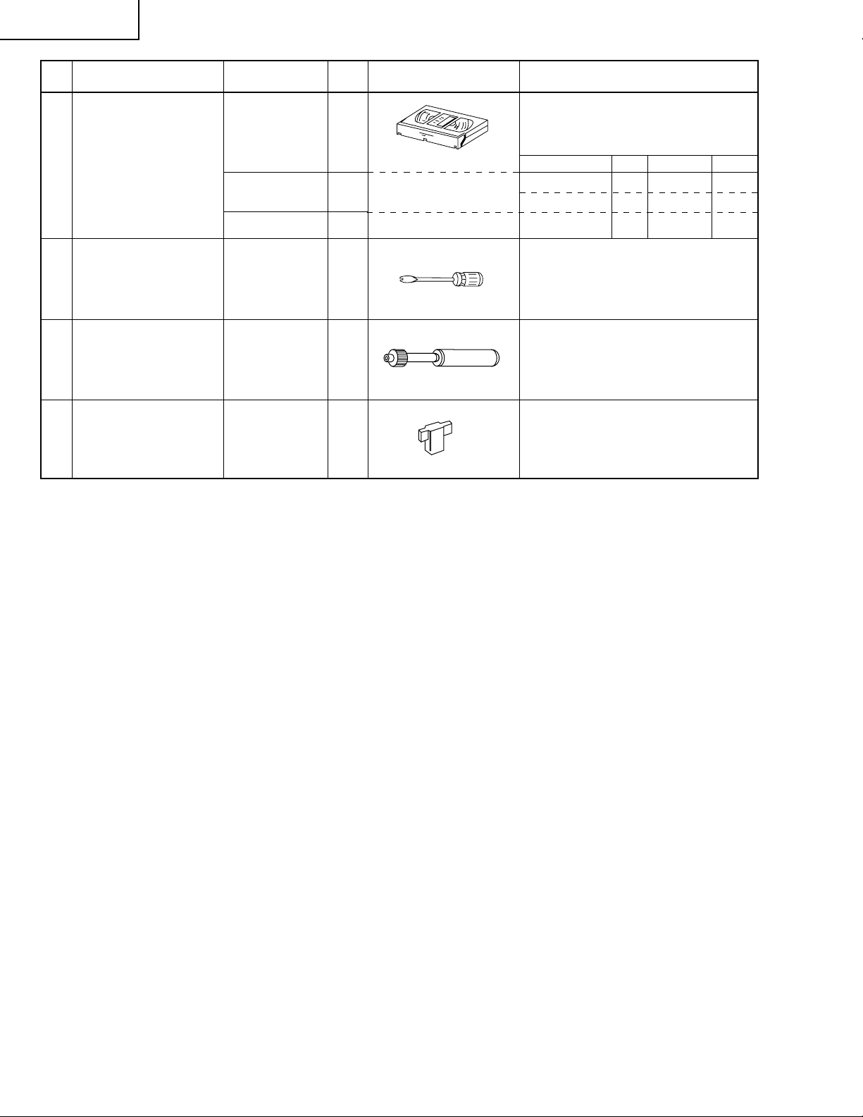
NOTE : Part replacement. : Cleaning : Apply grease
<Specified> Cleaning liquid Industrial ethyl alcohol
Maintained
Parts
Remarks
Ref.No.
500
hrs.
1000
hrs.
1500
hrs.
2000
hrs.
Possible symptom
encountered
Guide roller ass’y
Sup guide shaft
Reverse guide
Slant pole on pole base
Full erase head
A/C head
Upper and lower drum ass’y
Capstan D.D. motor
Pinch roller
Reel belt
Tension band ass’y
Loading motor
Idler ass’y
Limiter pulley
Supply/take-up main brake levers
AHC
(Automatic Head Cleaner)
49
—
19
7,8
58
59
63
61
12
34
1
60
46
48
24,25
26
Colour and beating
Small sound or sound
distortion
No tape running,
uneven colour
No tape running, tape
slack
No tape running, tape
slack, no fast forward/
rewind motion
Lateral noises Head
occasionally blocked
Abnormal rotation or significant
vibration requires replacement.
Clean tape contact part with the
specified cleaning liquid.
Clean tape contact area with
the specified cleaning liquid.
Replace the roller of the
cleaner when it wears down.
Just change the AHC roller
assembly for new one.
Screen swaying
Cassette not loaded or
unloaded
No tape running, tape
slack
Tape slack
Clean rubber and rubber
contact area with the specified
cleaning liquid.
Poor S/N ratio, no
colour Poor flatness
of the envelope with
alignment tape
* This mechanism does not need electric adjustment with variable resistor. Check parts. If any deviation is found,
clean or replace parts.
Perform the maintenance with the regular intervals as follows so as to maintain the quality of machine.
27DV-S100
27DV-CS10
Video head cleaning procedure
1. Apply one drop of cleaning liquid to the cleaning paper with the baby oiler.
2. Gently press the cleaning paper against the video head to fix your finger, and move the upper drum so that each
head is passed to and for 5 times (do not move the cleaning paper).
3. Wipe with the dry cleaning paper.
Notes :
• Use the commercially available ethanol of Class 1 as
cleaning liquid.
• Since the video head may be damaged, do not move
up and down the cleaning paper.
• Whenever the video head is cleaned, replace the
cleaning paper.
• Do not apply this procedure for the parts other than
the video head.
Gently press the cleaning paper to
fix with your finger, and rotate the
upper drum to clean.
Move to and for 5 times for each head.
(Do not move the cleaning paper.)
ZPAPRA56-001E Cleaning Paper
ZOiLR-02-24TE Babe Oiler (Spoit)
Rotate the upper drum
with one hand.
Parts Code Description
27
Page 28
27DV-S100
500g
Mechanism chassis
Weight to prevent
float (500g)
27DV-CS10
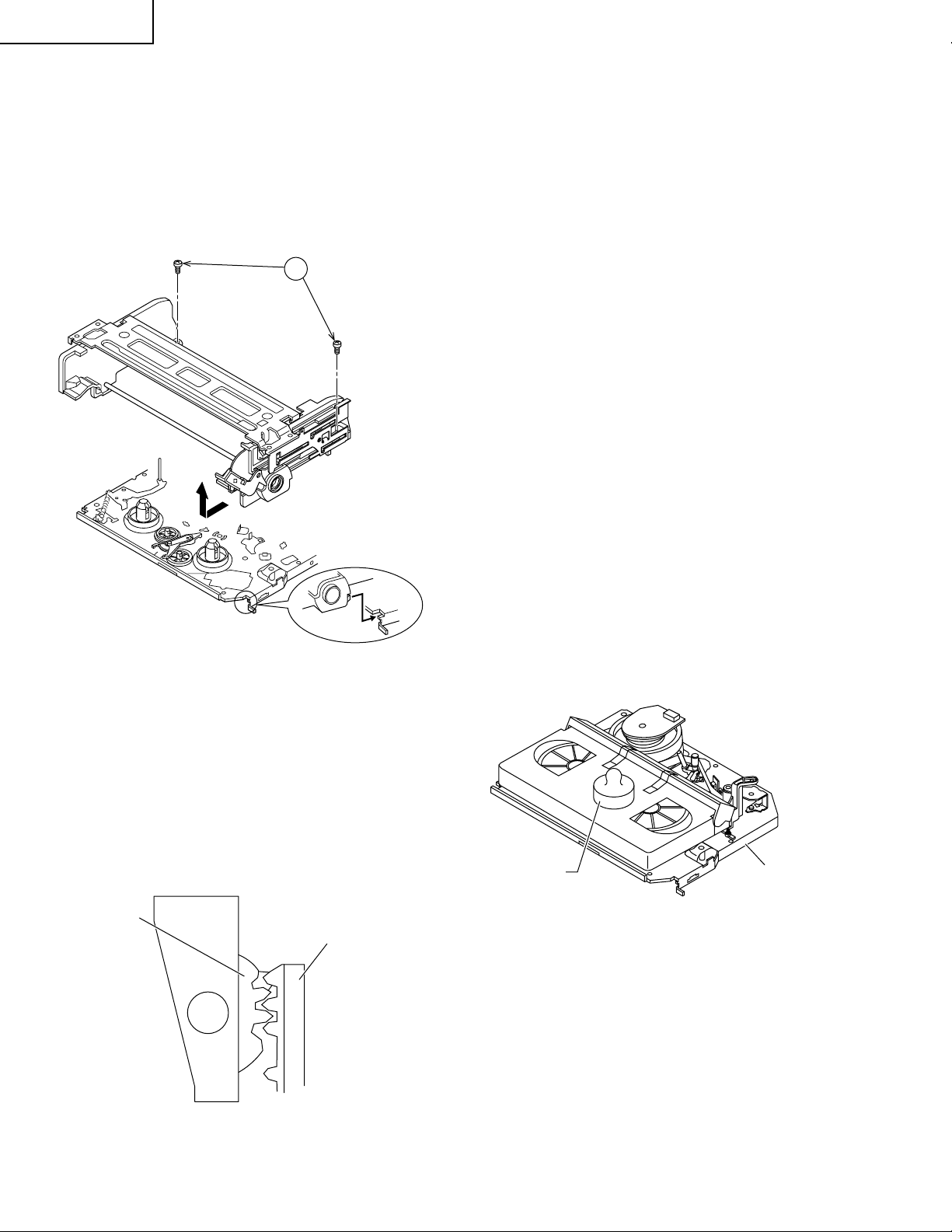
REMOVING AND INSTALLING THE CASSETTE HOUSING
• Removal
1. In the cassette removing mode, remove the cassette.
2. Unplug the power cord.
3. Remove in the following numerical order.
a) Remove two screws 1.
b) Slide and pull up the cassette housing control.
1
Figure 1-1.
Notes:
1. When fitting the S/E sensor holder to the cassette
controller frame L/R, take care.
2. Misengagement of teeth of casecon drive gear and
drive angle gear causes malfunction. (The cassette
cannot be set, load and ejection are repeated).
3. In the case when you use the magnet screw driver,
never approach the magnet driver to the A/C head, FE
head, and drum.
4. When installing or removing, take care so that the
cassette housing control and tool do not contact the
guide pin or drum.
5. After installing the cassette housing control once perform cassette loading operation.
TO RUN A TAPE WITHOUT THE CASSETTE
HOUSING CONTROL ASSEMBLY
1. Remove the full-surface panel.
2. Short-circuit R7057 and JUMPER:420.
3. Plug in the power cord.
4. Turn off the power switch.
(The mechanism moves to the cassette mounting
position.)
5. Open the lid of a cassette tape by hand.
6. Hold the lid with two pieces of vinyl tape.
7. Set the cassette tape in the mechanism chassis.
8. Stabilize the cassette tape with a weight (500g) to
prevent floating.
9. Turn on the power switch.
10. Perform running test.
11. After running test, once turn off the power to let the
mechanism move to the cassette mounting position,
then remove the cassette.
• Reassembly
1. Before installing the cassette housing control, shortcircuit R7057 and JUMPER:420 provided on the main
PWB, prug in the power cord, and then press the
STOP/EJECT button. The casecon drive gear turns
and stops when the positioning mark appears. Engage
two teeth of casecon drive gear with the three teeth of
casecon drive angle gear, and set on the mechanism
chassis as shown below.
Casecon
drive gear
Casecon drive
angle gear
Figure 1-2.
2. Install in the reverse order of removal.
Figure 1-3.
Note:
The weight should not be more than 500g.
To take out the cassette tape.
1. Turn off the power switch.
2. Take out the cassette tape.
28
Page 29
27DV-S100
27DV-CS10
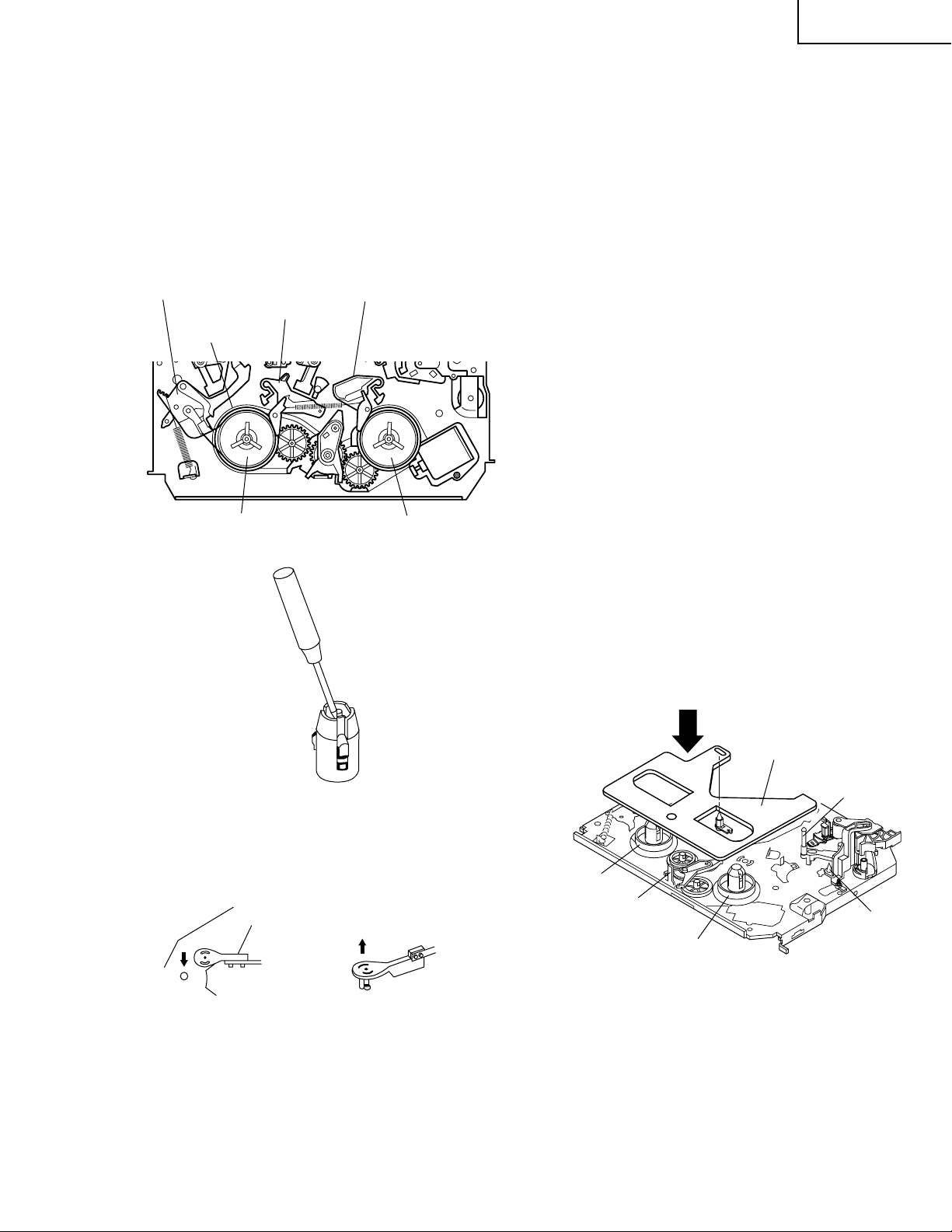
REEL DISK REPLACEMENT AND HEIGHT
CHECK
• Removal
1. Remove the cassette housing control assembly.
2. Pull the tension band out of the tension arm ass'y.
3. Remove the Supply/Take-up main brake ass'y.
4. Open the hook at the top of the reel disk, and remove
the reel disk.
Note:
Take care so that the tension band ass'y and main brake
ass'y (especially soft brake) are not deformed.
Tension arm ass'y
Supply main brake ass'y
Tension band ass'y
Supply reel disk
Take-up main brake ass'y
Take-up reel disk
3. After checking the reel disk height, wind the tension
band ass'y around the reel disk, and insert into the hole
of tension arm ass'y.
4. Assemble the Supply main brake ass'y.
Notes:
1. When installing the reel disk, take due care so that the
tension band ass'y is not deformed and grease does no
adhere.
2. Do not damage the Supply main brake ass'y. Be careful
so that grease does not adhere to the brake surface.
• Reassembly (Take-up reel disk)
1. Clean the reel disk shaft and apply grease (SC-141) to
it.
2. Align the phase of the reel disk to that of the reel relay
gear and to install a new take-up reel disk onto the
shaft.
3. Check the reel disk height and reassemble the take-up
main brake ass'y.
Note:
1. Take care so that the Take-up main brake ass'y is not
damaged. Take care so that grease does not adhere
the brake surface.
2. After reassembly, check the video search rewind back
tension (see page 32), and check the brake torque (see
page 34).
Figure 1-4.
Note:
When the tension band ass'y is pressed in the direction of
the arrow for removal, the catch is hard to be deformed.
Figure 1-5.
• Height checking and adjustment
Note:
1. Set the master plane with due care so that it does not
contact the drum.
2. When putting the master plane, shift the reverse guide
a little in the loading direction. Care must be taken
since excessive shift results in damage.
Master plane
Reverse
guide
Supply reel disk
Cassette lock
release shaft
Take-up reel disk
Position
pin
Figure 1-6.
• Reassembly (Supply reel disk)
1. Clean the reel disk shaft and apply grease (SC-141) to
it.
2. Match the phases of reel disk and reel relay gear, and
set the new reel disk.
Note:
Check that the reel disk is lower than part A but higher than
part B. If the height is not correct, readjust the reel disk
height by changing the poly-slider washer under the reel
disk.
• Problems caused by maladjustments
1. Tapes may get scratched.
29
Page 30
27DV-S100
27DV-CS10
Note:
Whenever replacing the reel disk, perform the height
checking and adjustment.
Master plane
10 ± 0.2mm
Reel disk
Reel disk
Reel disk height
adjusting jig
Mechanism chassis
A
B
Figure 1-7.
CHECKING AND ADJUSTMENT OF TAKEUP TORQUE IN FAST FORWARD MODE
• Remove the cassette housing control assembly.
• After short-circuiting R7057 and JUMPER:420
provided on the main PWB, plug in the power cord,
then turn on the power.
• Setting
1. Set a torque gauge to zero on the scale. Place it on the
take-up reel disk.
2. Press the FF button.
3. To calculate the remaining capacity of the play back
mode, slowly rotate the supply reel disk, and then shift
it into the forward mode.
• Checking
1. Turn the torque gauge slowly (one rotation every 2 to
3 seconds) by hand in the CW direction.
2. Make sure that the indication of torque gauge is not
less than 30mN·m (306gf·cm).
Torque gauge
Notes:
1. Hold the torque gauge by hand so that it is not moved.
2. Do not keep the reel disk in lock state. Do not allow
long-time measurement.
5. CHECKING AND ADJUSTMENT OF
TAKE-UP TORQUE IN REWIND MODE
• Remove the cassette housing control assembly.
• After short-circuiting R7057 and JUMPER:420
provided on the main PWB, plug in the power cord,
then turn on the power.
• Setting
1. Set a torque gauge to zero on the scale. Place it on the
supply reel disk.
2. Press the rewind button.
3. To calculate the remaining capacity, slowly rotate the
take-up reel disk, and then shift it into the rewind mode.
• Checking
1. Turn the torque gauge slowly (one rotation every 2 to
3 seconds) by hand in the CCW direction.
2. Make sure that the indication of torque gauge is not
less than 30mN·m (306gf·cm).
Torque gauge
30mN·m (306gf·cm)
or more
CCW
The gauge is held at
its maximum value.
(Red mark)
30mN·m (306gf·cm)
or more
Idler ass'y
Figure 1-8.
CW
The gauge is held at
its maximum value.
(Red mark)
• Adjustment
1. If the FF winding-up torque is less than the specified
value, clean the capstan D.D. motor pulley, drive belt,
and limiter pulley with cleaning liquid, and check again.
2. If the torque is less than the set value, replace the reel
belt.
• Problems caused by maladjustments
1. Tapes may fail to be wound up near the FF end.
Supply reel disk
Idler ass'y
Figure 1-9.
• Adjustment
1. If the rewind winding-up torque is less than the specified value, clean the capstan D.D. motor pulley, drive
belt, and limiter pulley with cleaning liquid, rewind
again, and check the winding-up torque.
2. If the winding-up torque is still out of range, replace the
drive belt.
• Problems caused by maladjustments
1. Tapes may fail to be wound up near the REW end.
30
Page 31

27DV-S100
27DV-CS10
Notes:
1. Hold the torque gauge by hand so that it is not moved.
2. Do not keep the reel disk in lock state. Do not allow
long-time measurement.
CHECKING AND ADJUSTMENT OF TAKEUP TORQUE IN RECORD/PLAYBACK
MODE
• Remove the cassette housing control assembly.
• After short-circuiting R7057 and JUMPER:420
provided on the main PWB, plug in the power cord.
• Turn off the power switch. (The mechanism moves
to the cassette mounting position.)
• Open the cassette torque meter lid, and fix it with
tape.
• Load the cassette torque meter into the unit.
• Put the weight (500g) on the cassette torque meter.
• Turn on the power switch.
• Press the picture record button, and set EP picture
record mode (x3).
Set value EP6.9 ± 2.5mN·m (70 ± 25gf·cm)
CHECKING AND ADJUSTMENT OF TAKEUP TORQUE IN VIDEO SEARCH REWIND
MODE
• Remove the cassette housing control assembly.
• After short-circuiting R7057 and JUMPER:420
provided on the main PWB, plug in the power cord,
then turn on the power.
• Setting
Press the playback button and rewind button to set the
video search rewinding mode.
• Checking
Place the torque gauge on the supply reel disk, and turn
it counterclockwise very slowly (one rotation every 1 to 2
seconds) and check that the torque is within the set value
14.0 ± 3.9mN⋅m. (144 ± 40gf⋅cm)
Torque gauge
CCW
500g
Cassette torque meter
Figure 1-10.
• Checking
1. Make sure that value is within the setting 6.9 ± 2.5mN·m
(70 ± 25gf·cm).
2. The winding-up torque fluctuates due to variation of
rotation torque of limiter pulley ass'y. Read the center
value of fluctuation as setting.
3. Set the EP record mode (x3) and make sure that the
winding-up torque is within setting.
• Adjustment
If the playback winding-up torque is not within the setting,
replace the limiter pulley assembly.
Note:
When the torque cassette is set, put a weight (500g) to
prevent rise.
When the cassette torque meter is taken out.
Turn off the power switch.
• Problems caused by maladjustments
1. Much maladjusted : Tapes may get scratched.
2. Slightly maladjusted : Tapes may get slack halfway,
resulting in the STOP mode.
: Tapes may get entangled.
Supply reel disk
Figure 1-11.
Note:
Surely put the torque gauge on the reel disk to measure.
If the torque gauge is raised, accurate measurement is
impossible.
• Adjustment
If the rewinding playback winding-up torque is not within
the setting, replace the limiter pulley assembly.
Note:
The winding-up torque fluctuates due to variation of
rotation torque of supply reel disk. Read the center value
of fluctuation as setting.
• Problems caused by maladjustments
1. Much maladjusted : Tapes may get scratched.
2. Slightly maladjusted : Tapes may get slack halfway,
resulting in the STOP mode.
: Images onscreen may get distorted.
: Tapes may get entangled.
: Tapes may became out from
cassette.
31
Page 32

27DV-S100
27DV-CS10
CHECKING THE VIDEO SEARCH REWIND
BACK TENSION
• Remove the cassette housing control assembly.
• After short-circuiting R7057 and JUMPER:420
provided on the main PWB, plug in the power cord,
then turn on the power.
• Checking
1. After pressing the play button, press the rewind button,
and set the video search rewind mode.
2. Place the torque gauge on the take-up reel disk, and
turn it counterclockwise very slowly (one rotation every
2 to 3 seconds) and check that the torque is within the
set value 3.4 ± 1.5mN⋅m (35 ± 15gf⋅cm).
• Problems caused by maladjustments
1. Tapes may get scratched whether much or slightly
maladjusted
Torque gauge
CCW
Tension gauge
Pinch roller
Capstan shaft
Tension gauge adapter
900 - 1,200gf
Figure 1-13.
1. Detach the pinch roller from the capstan shaft.
Do not separate excessively. Or the pinch lever and
pinch double action lever may disengage.
2. Engage the tension gauge adapter with the pinch roller
shaft, and pull in the arrow direction.
3. Gradually return the pinch roller, and measure the
pulling force when the pinch roller contacts the capstan
shaft.
4. Make sure that the measured value is within setting 9.0
N to 11.8 N (900 to 1,200gf).
Take-up reel disk
Figure 1-12.
Note:
Set the torque gauge securely on the take-up reel disk. If
it is not secure, the measurement will be incorrect.
CHECKING THE PINCH ROLLER
PRESSURE
• Remove the cassette housing control assembly.
• After short-circuiting R7057 and JUMPER:420
provided on the main PWB, plug in the power cord,
then turn on the power.
• Checking
Press the play button to set the playback mode.
• Problems caused by maladjustments
1. Much maladjusted : The service life of the capstan
and pinch roller may be shorter.
2. Slightly maladjusted : Images onscreen may get
distorted.
CHECKING AND ADJUSTMENT OF
TENSION POLE POSITION
• Remove the cassette housing control assembly.
• After short-circuiting R7057 and JUMPER:420
provided on the main PWB, plug in the power cord,
then turn off the power.
• Setting
1. Turn off the power switch.
2. Open the cassette tape (T-120), and fix with tape.
3. Set the cassette tape into the unit.
4. Put the weight (500g) on the cassette tape.
5. Turn on the power switch.
6. Make the adjustment with the beginning of a T-120
tape.
500g
Weight to prevent
float (500g)
Figure 1-14.
• Checking
1. Set a cassette tape, push the REC button to place the
unit in the SP record mode. Now check the tension pole
position.
(T-120)
32
Page 33

27DV-S100
90°
90°
Tension pole adjuster
500g
Weight to prevent
float (500g)
Cassette torque
meter
27DV-CS10
2. Visually check to see if the right edge of the tension
pole is within the 2.3 ± 0.25 from the right edge of the
Sup guide shaft.
Sup guide shaft
Tension pole
2.3 ± 0.25
Make the adjustment with the beginning of a T-120 tape.
Figure 1-15.
At left side from the center line
Tension pole adjuster adjusting range
Figure 1-18.
Adjust so that the delta mark of tension pole adjuster is
within 90° range (left, right).
CHECKING AND ADJUSTMENT OF
RECORD/PLAYBACK BACK TENSION
• Remove the cassette housing control assembly.
2.3 ± 0.25
Figure 1-16.
Insert the slotted screwdriver in the tension pole adjuster,
and rotate counterclockwise.
At right side from the center line
2.3 ± 0.25
Figure 1-17.
Insert the slotted screwdriver in the tension pole adjuster,
and rotate clockwise.
• Problems caused by maladjustments
1. Images onscreen may get distorted.
• After short-circuiting R7057 and JUMPER:420
provided on the main PWB, plug in the power cord,
then turn off the power.
• Setting
1. Turn off the power switch.
2. Open the torque cassette meter and fix with tape.
3. Set the cassette tape into the unit.
4. Put the weight (500g) on the cassette torque meter.
5. Turn on the power switch.
Figure 1-19.
• Checking
1. Push the REC button to place the unit in the SP record
mode.
2. At this time ascertain that the back tension is within the
setting (36.5 to 52g·cm) by seeing the indication of
torque cassette meter.
33
Page 34

27DV-S100
27DV-CS10
• Adjustment
1. If the indication of torque cassette meter is lower than
the setting, shift the tension spring engagement to the
part A.
2. If the indication of torque cassette meter is higher than
the setting, shift the tension spring engagement to the
part B.
• Problems caused by maladjustments
1. Much maladjusted : Tapes may get scratched.
2. Slightly maladjusted : Images onscreen may get
distorted.
BA
Tension arm
Tension spring
Figure 1-20.
CHECKING THE BRAKE TORQUE
• Checking the brake torque at the supply side
in the CW direction/CCW direction with respect to the
supply reel disk so that the reel disk and torque gauge
pointer rotate at equal speed, and make sure that the
value is within the setting (CW direction: 4.9 to 13.7mN·m
(50 to 140gf·cm); CCW direction: 2.9 to 9.8mN·m (30 to
100gf·cm).
• Checking the brake torque at the take-up side
Torque gauge
CW
Take-up reel
disk
CCW: 4.9~13.7mN⋅m (50~140gf⋅cm)
CW: 3.9~10.8mN⋅m (40~110gf⋅cm)
CCW
Figure 1-22.
• Remove the cassette housing control assembly.
Torque gauge
CCW
CCW: 2.9~9.8mN⋅m (30~100gf⋅cm)
CW: 4.9~13.7mN⋅m (50~140gf⋅cm)
CW
Supply reel disk
Figure 1-21.
• Remove the cassette housing control assembly.
• After short-circuiting R7057 and JUMPER:420
provided on the main PWB, plug in the power cord,
then turn on the power.
• Setting
1. Set a torque gauge to zero on the scale. Place it on the
supply reel disk.
2. Switch from the FF mode to the STOP mode.
3. Disconnect the power cord.
• Checking
Turn the torque gauge at a rate of about one turn/2 sec
• After short-circuiting R7057 and JUMPER:420
provided on the main PWB, plug in the power cord,
then turn on the power.
• Setting
1. Switch from the FF mode to the STOP mode.
2. Disconnect the power cord.
3. Set a torque gauge to zero on the scale. Place it on the
take-up reel disk.
• Checking
1. Turn the torque gauge at a rate of about one turn/2 sec
in the CCW direction/CW direction so that the reel disk
and torque gauge pointer rotates at equal speed and
make sure that the value is within the setting (CCW
direction: 4.9 to 13.7mN·m (50 to 140gf·cm), CW
direction: 3.9 to 10.8 mN·m (40 to 110gf·cm).
2. Adjustment of the brake torque at the supply side and
the take-up side
• Unless the supply side brake torque or take-up side
brake torque is within the setting, clean the felt surface
of reel disk (supply, take-up) brake lever, check again
the brake torque.
• If value cannot be set within the setting yet, replace the
main brake ass'y or main brake spring.
• Problems caused by maladjustments
1. From the FF or REW to the STOP mode
• Much maladjusted :The brake noise may get louder.
• Slightly maladjusted :Tapes may get slack and
scratched.
34
Page 35

27DV-S100
27DV-CS10
REPLACEMENT OF A/C (Audio/Control)
HEAD
1. Remove the cassette housing control assembly.
2. In unloading state unplug the power cord.
• Removal
1. Remove the screws 123, Azimuth screw, Tilt screw.
2. Unsolder the PWB fitted to the A/C head.
Notes:
1. When replacing, never touch the head. If you touched,
clean with the cleaning liquid.
2. When removing the screw 3, take care so that the
spring may out.
3
Azimuth screw
Spring
2
Figure 1-23.
Tilt screw
Height screw
1
section and A/C head front section) (See the figure be-
low.)
3. Align the left end of gear of A/C head arm with the
punched mark of chassis, tentatively tighten the screws
1 and 2 so as to ensure smooth motion of A/C head
arm. Tentative tightening torque must be 0.15 to 0.20
N·m (1.5 to 2.0kgf·cm).
1
3
Height screw
Left end of A/C head plate gear
2
Punched line mark on chassis
Figure 1-25.
Notes:
1. If the screws 1 and 2 are tighten tentatively too
loose, the azimuth and height of A/C head may change
when they are finally tightened. Therefore care must be
taken.
2. After completion of A/C head be sure to adjust tape
running. (Execute the running adjustment by the method
described in page 37.)
• Replacement
1. Solder the removed PWB to the new head assembly.
2. Adjust the height from the A/C head plate (lower
surface) to the A/C head base to 10.8mm with slide
calipers. (3 places of azimuth screw section, tilt screw
Solder
New A/C head ass'y
A/C head PWB
Never touch the head
A/C head base
10.8mm10.8mm
Figure 1-24.
35
Page 36

27DV-S100
27DV-CS10
A/C HEAD HEIGHT ROUGH ADJUSTMENT
• Setting
Height screw
Weight to prevent
float (500g)
Azimuth screw
Tilt screw
Cassette tape
500g
Mechanism chassis
Figure 1-26.
HEIGHT ADJUSTMENT OF REVERSE
GUIDE
1. Adjust the height from the mechanism chassis to the
reverse guide lower flange to 13.38 mm, using the
reverse guide height adjustment jig, in tape loading
state. (Refer to Figure 1-28 (a) (b).)
Reverse guide height
Reverse guide
adjusting jig
(a) (b)
Figure 1-28.
2. Rotate counterclockwise the reverse guide height adjustment nut 1/10 turn. (For height adjustment use the
reverse guide height adjustment box driver (JiGDRiVER
11055)).
Reverse guide height
adjusting jig
Mechanism
chassis
Box driver
13.38mm
1. Set the cassette tape in the unit.
2. Press the PLAY button to put the unit in the playback
mode.
3. Roughly adjust the height of the A/C head by turning
the height screw until the tape is in the position shown
below.
A/C head
Tape
0.3mm
Figure 1-27.
• Adjustment
Adjust the height screw visually so that the control head is
visible 0.3mm below the bottom of the tape.
• Problems caused by maladjustments
1. Tapes may get scratched
2. Images onscreen distorted.
CCW
Height adjusting nut
Figure 1-29.
3. Set the tape, and check for tape crease near the
reverse guide in the playback mode.
If crease is found, turn the reverse guide adjustment
nut to remove crease. (As for crease check refer to
Figure 1-30.)
500g
Weight to
prevent float (500g)
A
Mechanism
chassis
Reverse guide
Capstan
motor shaft
Fixing guide
An example of
crease near the
reverse guide
* Check for crease from the A direction.
Figure 1-30.
• Problems caused by maladjustments
1. Tapes may get scratched.
36
Page 37

27DV-S100
27DV-CS10
ADJUSTMENT OF TAPE DRIVE TRAIN
1. Tape run rough adjustment
1 Remove the cassette housing control assembly.
2 After shortcircuiting R7057 and JUMPER:420
provided on the main PWB, plug in the power cord.
, then turn off the power. Set the tape for each check
and / or adjustment shown below and turn on the
power.
3 Check and adjust the position of the tension pole.
(See page 33.)
4 Check and adjust the video search rewind back
tension. (See page 32.)
5 Connect the oscilloscope to the test point for PB
CHROMA envelope output (TP3301). Set the synchronism of the oscilloscope to EXT. The PB
CHROMA signal is to be triggered by the head
switching pulse (TP3302).
6 Set the alignment tape (VROATSV) to play. (Put a
500g weight on the cassette tape to prevent lift of
cassette tape.)
Guide roller
Cassette Tape
500g
tion, and adjust the envelop waveform to maximum
with X value adjustment nut. Thereby the tape run
rough adjustment is facilitated.
2. Especially the outlet side envelope waveform must
have higher flatness.
Figure 1-32.
2. Adjustment of A/C head height and azimuth
1 Perform the initial setting of A/C head position by
the method stated in "page 35 Replacement 3".
2 Connect the oscilloscope to the audio output
termina0l (TP6601).
3 Using the alignment tape in which 1 kHz linear
audio signal has been recorded, adjust the height
screw so as to get max audio output.
4 Using the alignment tape in which 7 kHz linear
audio signal has been recorded, adjust the azimuth
screw so as to get max audio output.
5 The adjustment of 3 and 4 twice or three times
repeat, and finally adjust 4.
Weight of 500g
Figure 1-31.
7 Press the tracking button (+), (–) and change the
envelope waveform from max to min and from min
to max. At this time make sure that the envelope
waveform changes nearly parallel.
8 Unless the envelope waveform changes nearly
parallel, adjust the height of supply side and takeup side guide roller so that the envelope waveform
changes nearly parallel. (For envelop adjustment
procedure refer to Figure 1-35.)
9 Turn the tilt screw to remove the tape crease at the
fixing guide flange.
Playback the tape and check for tape crease at the
fixing guide flange.
(1)If there is no tape crease
Turn the tilt screw clockwise so that tape crease
appears once at the flange, and then return the
tilt screw so that the crease disappears.
(2)If there is tape crease
Turn counterclockwise the tilt screw so that the
tape crease disappears.
(Reference) If the tilt screw is turned clockwise
crease appears at the lower flange.
• Problems caused by maladjustments
1. Totally maladjusted
• Images onscreen may get distorted or affected by
noises, or may fail to appear.
Notes:
1. Previously set the tracking control in the center posi-
For X value adjustment
Adjust the X value, turning the
gear-type screwdriver.
Figure 1-33.
3. Tape run adjustment
1 Connect the oscilloscope to PB CHROMA enve-
lope output test point, set oscilloscope sync to EXT,
trigger-input the PB CHROMA signal (head switching pulse).
2 Rough adjustment of X value
Tentatively fix A/C head arm screws 1 and 2 by the
method described in page 35 "Replacement 3".
After shortcircuiting R7057 and JUMPER:420, plug
in the powercord, then turn off the power. And set
the alignment tape (VROATSV) into the unit, turn
on the power, then playback it. As a result the autotracking is automatically cancelled, so that the X
value adjustment mode is set.
Move the A/C head with the X value adjustment
gear driver (JiGDRiVER-6) by the method shown in
Figure 1-33, and adjust the A/C head so as to get
the maximum envelope waveform. (Note: When
the A/C head is adjusted, adjust so that the maximum envelop waveform is obtained nearest the
position of initial setting made in page 35.)
37
Page 38

27DV-S100
27DV-CS10
3 Next, change the alignment top to VROEFZCS to
play back. Press the tracking button (+), (–) and
change the envelope waveform from max to min
and from min to max. At this time adjust the height
of supply and take-up side guide roller with the
adjustment driver (JiGDRiVERH-4) so that the envelope waveform changes nearly parallel.
4 If the tape is lifted or sunk from the helical lead
surface, the PB CHROMA envelope waveform appears as shown in Figure 1-35.
5 Press the tracking button (+), (–) and make sure
that the envelope waveform changes nearly parallel.
6 Finally check tape crease near the reverse guide. If
tape crease is found, remove it as stated in page 36
"HEIGHT ADJUSTMENT OF REVERSE GUIDE"
item 3.
Supply side
Take-up side Supply side Take-up side
PB CHROMA
Envelope
CH-1 CH-2
Head switching pulse
Figure 1-34.
4. A/C head X value adjustment
1 Tentatively fix A/C head arm screws 1 and 2 by the
method described in page 35 "Replacement 3".
2 After shortcircuiting R7057 and JUMPER:420, plug
in the powercord, then turn off the power. And set
the alignment tape (VROEFZCS) into the unit, turn
on the power, then playback it. As a result the autotracking is automatically cancelled, so that the X
value adjustment mode is set.
When the tape is below the helical lead.When the tape is above the helical lead.
Adjustment
Supply side guide roller
rotated in clockwise
direction (lowers guide
roller) to flatten
envelope.
Take-up side guide roller
rotated in clockwise
direction (lowers guide
roller) to flatten
envelope.
Figure 1-35.
3 Move the A/C head with the X value adjustment
gear driver by the method shown in Figure 1-33,
and adjust the A/C head so as to get the maximum
envelope waveform. (Note: At this time adjust so as
to get the maximum envelope waveform nearest
the A/C head position which has been set in case of
X value rough adjustment as stated in page 37, 3-
2.)
4 Tighten finally the screws 1 and 2. Be sure to
tighten at first the screw 1 and then the screw 2.
Final tightening torque is 0.6N·m (If the screw 2 is
tightened first, the X value may deviate.)
5 Adjust the playback switching point (Refer to the
electric adjustment method.)
6 Playback the self-picture-recorded tape, and check
the flatness of envelope waveform and sound.
Supply side guide roller
rotated in counterclockwise direction (raises
guide roller) to make the
tape float above the helical
lead. The supply
side guide roller is then
rotated in the clockwise
direction to flatten the
envelope.
Take-up side guide roller
rotated in counterclockwise direction (raises
guide roller) to make the
tape float above the
helical lead. The take-up
side guide roller is then
rotated in the clockwise
direction to flatten the
envelope.
• Problems caused by maladjustments
1. Totally maladjusted
• Tapes may get scratched.
• Images onscreen may get distorted or affected by
noises, or may fail to appear.
• The linear audio level may get degraded.
Note:
When the A/C head X value adjustment is performed, be
sure to perform at first X value rough adjustment (refer to
page 37, 3-2).
2
1
38
Figure 1-36.
Page 39

27DV-S100
27DV-CS10
REPLACEMENT OF THE CAPSTAN D.D.
(DIRECT DRIVE) MOTOR
• Removal (Follow the order of indicated numbers.)
1. Remove the reel belt 1.
2. Remove the slow brake lever 2.
3. Remove the three screws 3.
3
Capstan D.D. motor
control PWB
Capstan D.D.
motor
Reel belt
1
Slow Brake Lever
Figure 1-37-1.
2
REPLACEMENT OF DRUM D.D. MOTOR
1. Set the ejection mode.
2. Withdraw the main power plug from the socket.
• Removal (Perform in numerical order.)
1. Disconnect the FFC cable 1.
2. Unscrew the D.D. stator assembly fixing screws 2.
3. Take out the D.D. stator assembly 3.
4. Unscrew the D.D. rotor assembly fixing screws 4.
5. Take out the D.D. rotor assembly 5.
Notes:
1. In removing the D.D. stator assembly, part of the drum
earth spring pops out of the pre-load collar.
Be careful not to lose it.
2. Install, so that the D.D. rotor ass'y and upper drum
ass'y mounting direction check holes align.
(Align the upper drum dent with the rotor hole.)
3. Be careful not to damage the upper drum or the video
head.
4. Protect the hole elements from shock due to contact
with D.D. stator or D.D. rotor ass'y.
5. After installation adjust the playback switching point for
adjustment of servo circuit.
2
D.D. stator ass'y
• Reassembly
1. Taking care so that the capstan shaft does not contact
the mechanism chassis, set its position on the mechanism chassis, and then install with the three screws.
2. Install the slow brake lever.
3. Install the reel belt.
Notes:
1. Before installing the capstan D.D. motor, confirm
whether an acetate tape (ZTAPEN120020E) is drawn
on the back of mechanism chassis.
Stick on acetate tape on the
projection part of the chassis.
Capstan Motor
Installation posltion.
MechanismChassis from the back.
Figure 1-37-2.
2. After installing the capstan D.D. motor, be sure to
rotate the capstan D.D. motor and check the movement.
3. Set the tape, and check for the tape crease near the
reverse guide in the playback mode. Adjust the A/C
head and azimuth as stated in page 37 item 2. If crease
is found, adjust as stated in page 36 "HEIGHT ADJUSTMENT OF REVERSE GUIDE".
3
1
4
5
4
D.D. rotor ass'y
Upper drum
Figure 1-38.
39
Page 40

27DV-S100
27DV-CS10
REPLACING THE UPPER AND LOWER
DRUM ASSEMBLY
• Replacement (Perform in the numerical order)
1 Remove the motor as stated in page 39 D.D. motor
replacement.
2 Remove the drum earth brush ass’y 2.
3 Remove the drum base 3 from the upper and lower
drum assembly 1.
[Cares when replacing the drum]
1. Be careful so that the drum earth brush is not lost.
2. Do not touch directly the drum surface.
3. Fit gently the screwdriver to the screws.
4. Since the drum assembly is an extremely precise
assembly, it must be handled with utmost care.
5. Make sure that the drum surface is free from dust, dirt
and foreign substances.
6. After replacing the drum be sure to perform the tape
running adjustment.
After that, perform also the electrical adjustment.
• Playback switching point adjustment
• X-position adjustment and check
• Standard and x-3 slow tracking adjustment
7. After replacing the drum clean the drum.
ASSEMBLING OF PHASE MATCHING
MECHANISM COMPONENTS
• Assemble the phase matching mechanism components in the following order.
1. Assemble the pinch roller assembly and pinch drive
cam.
2. Mounting the shifter (on the back of the mechanism
chassis).
3. Mounting the master cam (on the back of the mechanism chassis).
4. Assemble the connection gear, slow brake and loading
motor parts.
• Pinch drive cam and pinch roller assembling
method.
(Place the following parts in position in numerical order.)
(1)Reverse drive lever 1
(2)Reverse guide spring 2
(3)Reverse guide lever ass’y 3
(4)Reverse guide height adjusting nut 4
(5)Pinch drive cam 5
(6)Pinch roller ass’y 6
(7)Open lever 7
7
6
2
1
3
Figure 1-40.
4
3
1
2
5
Figure 1-39.
40
Page 41

1Insert Reverse Guide Lever Ass’y
27DV-S100
27DV-CS10
Insert reverse guide lever ass'y
2 Insert pinch drive cam
Turn the reverse guide lever
assembly counterclockwise
to the stopper.
Pinch drive lever ass'y
Fit the pinch drive cam so that the notch of pinch
drive cam aligns with the dent of pinch drive lever
assembly.
Fit the pinch drive cam so that the notch of
pinch drive lever assembly aligns with the
half-round notch of chassis.
Figure 1-41-1.
2Insert Pinch Roller/Pinch Double Action Lever Ass’y.
Pinch Roller Double
Action Lever Ass'y
Phase Matching Point 2
Align here.
3Insert Open Lever.
Open lever
Figure 1-41-2.
Figure 1-41-3.
41
Page 42

27DV-S100
27DV-CS10
INSTALLING THE SHIFTER
Capstan
D.D. motor
Reel pulley
(Bottom side of mechanism chassis)
Figure 1-42.
Insert
point 3
Insert
point 2
Drum
1. Make sure that the loading gear is at the PhaseMatching point 1 as shown below.
2. Install, paying attention to insert point 5 and release
point 3.
3. For the phase matching at the insert point 1, see the
Phase-Matching point 2 as shown below.
4. Finally fix the inserts 1 and 4.
Phase-Matching
point 2
Loading gear (T)
Round mark
Sifter
Half round notch
Insert
point 4
Insert
point 1
Shaft 1
Phase-matching
point 1
Shaft 1
Rotation
point 2
Shaft 1
Figure 1-43.
Shaft 2
Release
point 3
Insert
point 5
42
Page 43

27DV-S100
No grease
Apply grease
Apply grease
27DV-CS10
INSTALLING THE MASTER CAM (AT REAR
SIDE OF MECHANISM CHASSIS)
1. Make sure beforehand that the shifter is at the point as
shown below.
2. Place the master cam in the position as shown below.
E ring
(XRESJ30-06000)
Master cam
Fully turn
clockwise
Fully turn counterclockwise
Face the wide tooth side ward
Figure 1-44-1.
Note:
See the figure below for the phase matching between the
master cam and the casecon drive gear.
3. Finally fix with the E ring.
Master cam
REPLACEMENT OF LOADING MOTOR
• Removal
Figure 1-45.
Casecon drive gear
Round mark
When installing the master cam,
align the casecon drive gear
round mark with the half-round
notch of master cam.
Figure 1-44-2.
Half-round notch
• Replacement
Remove the loading motor, and install the replacement
loading motor as shown below.
+0
10.2 mm
–0.2
Figure 1-46.
The loading motor pressing-in must be less than 147 N
(15kgf).
Adjust the distance between motor and pulley to 10.2
+0.2
mm).
–0.2
43
Page 44

27DV-S100
27DV-CS10
ASSEMBLY OF CASSETTE HOUSING
1. Drive Gear and R Drive angle ass’y
Apply grease
MSPRT0381AJFJ
Apply grease
Apply grease
2. Synchro Gear, Drive Gear L and Drive Gear R
Top surface should be free from scratches or soil.
Figure 1-47.
LANGF9592AJFW
Drive angle
Drive gear R
Frame
Figure 1-48.
44
Page 45

27DV-S100
27DV-CS10
ADJUSTMENT OF THE VCR ELECTRICAL CIRCUITRY
Notes:
• Before the adjustment:
Electrical adjustments discussed here are often required after replacement of electronic components and mechanical
parts such as video heads.
Check that the mechanism and all electric components are in good working condition prior to the adjustments,otherwise
adjustments cannot be completed.
• Instruments required:
• Blank video cassette tape • Alignment tape (VROATSV)
Figure 2-1.
45
Page 46

27DV-S100
27DV-CS10
VCR SERVO CIRCUIT ADJUSTMENT
Note: The procedure of the adjustments is HEAD SWITCHING POINT → SLOW TRACKING PRESET
→ FV of STILL PICTURE
ADJUSTMENT OF HEAD SWITCHING POINT
1. Playback the alignment tape. (VROATSV)
2. Press both REC key and V OL-DO WN ke y on the front panel more than 2 seconds to turn the unit into the adjustment
mode. (PROGRAM TIMER LED is lighting and “T” is displayed on the monitor screen.)
3. Press PLAY key.
4. Automatically head switching point adjustment is started, and the unit will be back to PB mode after the adjustment
is finished.(PROGRAM TIMER LED is putting out)
5. Press STOP key.
ADJUSTMENT OF SLOW TRACKING PRESET
1. Playback SP and EP mode self recorded tape.
2. Playback SP mode recorded portion at slow mode.
3. Press both REC key and VOL-DOWN key on the front panel more than 2 seconds to turn the unit into the
adjustment mode. (PROGRAM TIMER LED is lighting and “T” is displayed on the monitor screen.)
4. Press SLOW key.
5. Automatically adjustment start, and the unit will be back to slow mode after the adjustment is finished. (PR OGRAM
TIMER LED is putting out).
6. To check the still noise, push PLAY key and then STILL key.
7. Next playback EP mode recorded portion at slow mode.
8. As same as 2-6 items, adjust EP mode slow tracking preset and EP mode noise.
ADJUSTMENT OF FV (False Vertical Sync) OF STILL PICTURE
1. Play a cassette which was self-recorded by the unit in SP mode.
2. Press the PAUSE/STILL button to freeze the picture.
3. Look at the monitor screen and adjust the TRACKING (+) and / or (–) b uttons so that the v ertical jitter of the picture
is minimized.
4. Play and freeze the self-recorded tape in EP mode and make sure the vertical jitter of the picture is not noticeable.
46
Page 47

TEST MODE OF DVD SECTION
The preparation date display of the program
10000000 ~~~~~~~~
(Last update)
Model number display
10000001 0000D031
(Model number)
The version display of the program
10000002 ~~~~~~~~
(Program version)
Region number display
10000003 00000001
(Region code: binary display)
Micro-code number display
10000004 ~~~~~~~~
(Micro-code version)
The preparation date display of the servo program
10000005 ~~~~~~~~
(Servo version)
Check mode of the DVD program contents
Press the "1" key on the remote control or the "STOP" key on the main unit.
(DVD test mode)
Laser test mode
Press the "1" key.
Press the "3" key. (to turn the unit into the dynamic test mode.)
(Turn the power off to cancel the dynamic test mode.)
(Unplug the AC cord to cancel the laser test mode.)
Press the "PLAY" key.
Press the "PLAY" key.
Press the "PLAY" key.
Press the "PLAY" key.
Press the"PLAY" key.
The display is returned to the initial screen
of the test mde.
Press the"PLAY" key.
Press the "1" key.
To (1)
Micro-code means the process
program of the system IC.
The tray opens, the DVD laser is lit, the spindle turns momentary
and the sled moves to the outer side.
"NO DISC" state
Press both of the "PLAY" key and the "STOP" key on the DVD front panel of the main unit
for 5 seconds during the DVD mode to turn the unit into the DVD test mode.
(Turn the power off to cancel the test mode.)
F0000000 00000000
DYNAMIC TEST
30000000 00000000
LASER TEST
30000001 000000DD
Press the "1" key.
The DVD laser goes out, the CD laser is lit,
the spindle turns momentary and the sled moves to the outer side.
LASER TEST
30000001 000000CD
Press the "1" key.
The DVD and CD lasers go out,
the spindle turns momentary and the sled moves to the outer side.
LASER TEST
30000001 00000000
27DV-S100
27DV-CS10
47
Page 48

27DV-S100
27DV-CS10
From (1) (dynamic test mode)
Step test mode
Press the "2" key.
STEP TEST
30000001 00000000
Press the "OPEN/CLOSE" key. (to close the tray.)
STEP TEST
30000200 00000000
STEP TEST
30000201 00000000
Press the "PLAY" key.
STEP TEST
30000202 00000000
Press the "PLAY" key.
STEP TEST
30000203 00000000
Press the "PLAY" key.
STEP TEST
30000204 00000000
Press the "PLAY" key.
STEP TEST
30000205 00000000
Press the "PLAY" key.
(DVD operation)
STEP TEST
DD000210 00000000
STEP TEST
DD000211 00000000
Press the "PLAY" key.
STEP TEST END
DD000212 ~~~~~~~~
(~~~~~~~~ is sector ID (address))
(Unplug the AC cord to cancel the step test mode.)
Put a disc on the tray after the tray is opened.
(loading the disc)
Focus on
RF gain adjustment, Tracking on
Focus gain adjustment
Tracking gain adjustment
Focus balance adjustment
In case of 2–layer DVD,
RF gain, focus gain and
focus balance adjustments
of layer 0.
Reading control data
Tracing playback mode
(CD operation)
STEP TEST END
CD000210 ~~~~~~~~
(~~~~~~~~ is SUB-Q (address))
Tracing playback mode
after reading TOC.
(TOC: Table of Contents)
To (2)
Tracing playback, jump test mode
Press the "3" key.
PLAY TEST
30000001 00000000
Press the "OPEN/CLOSE" key. (to close the tray.)
PLAY TEST
DD000302 ~~~~~~~~
Pressing the keys on the remote control mentioned in the table below
enables the jump test.
(Unplug the AC cord to cancel the tracing playback, jump test mode.)
Key
1
4
7
CLEAR
2
5
8
SKIP/REV
Put a disc on the tray after the tray is opened.
Tracing playback mode (~~~~~~~~ is sector ID (address))
Jump
–15000
–1
–102
–510
–511
–765
–766
–7000
Key
3
6
9
MEMORY
REPEAT
PROGRAM
SKIP/FWD
Jump
1
102
510
511
765
7000
15000
48
Page 49

Spindle offset adjustment mode
Press the "DISC MENU" key.
(When the adjustment is complete, the unit turns back to the dynamic test mode,
and "3000000 00000000" is displayed on the screen.)
Tray is opened.
From (2) (dynamic test mode)
SPIN OFFSET
(The spindle offset is adjusted automatically.)
The adjustment result is indicated in the ~~~~ portion.
ADJUST COMPLETE
00000000 00000~~~~
[ROM REWRITING MODE]
This mode is able to update the version of the DVD program.
Please confirm the program version according to the procedure for the DVD test mode before you start the rewriting.
1. Connect a computer to the unit as shown below. Start the rewriting software of the computer.
2. Pressing both of the "PLAY" key and the "SKIP/FWD" key on the DVD front panel of the unit, turn the power on.
(Keep on pressing both keys for 3 seconds or so.)
The unit turns into the ROM rewriting mode, and the VCR indicator starts flashing at 1Hz.
3. Following the computer’s onscreen message, type in "Y" and press "ENTER" key. When the command for the data
transfer starts the rewriting job, the VCR indicator and the DVD indicator are alternately flashing at 1Hz.
4.When the rewriting is complete, only the DVD indicator keeps on flashing at 1Hz.
5.Finally press the "STOP" key of the DVD and turn the power off.
Computer
(DOS)
TV/VCR/DVD
27DV-S100
27DV-CS10
ROM writing tool
Connect to the DIGITAL OUT terminal.
27DV-S100
27DV-CS10
49
Page 50

MECHANISM OPERATION FLOWCHART
* This flowchart describes the outline of the mechanism’s operation, but does not give its details.
CASSETTE INSERTION STOP
End
27DV-S100
MECHANISM OPERATION FLOWCHART AND TROUBLESHOOTING GUIDE
27DV-CS10
50
G mechanical timing
Mode check
Cam mark
Mode detection outside
(D709 SW B)
Mode detection inside
(D708 SW A)
Mode detection outside
Mode detection inside
S sensor
S sensor
25
20
15
10
5
0
CA/END
CS/EJ
0 19.812 81 179 233200 265 282 316 334
10.354 12.812
EJ UL PU PU2 VSR PB SLW FF STP
0
0
1
1
1
1
Open
Close
60 120 180 240 300 380
0
0
101
0
0
0
0
0
1
1 or 0
CS/EJ
ULD
PU1
PU2
VSR
PB
SLOW
FF
STOP
Cam graph E
UL
1
1
10111110100010100010000010
Mode detection inside
sensor A
1
1
1
0
0
0
0
0
0
PU1
Mode detection outside
sensor B
0
1
1
1
1
0
1
1
0
PU2
VSR
PB SLOW
Insert cassette.
Cassette is ejected and loading
motor stops.
Double action rack slides.
Start sensor close.
Loading motor starts in normal
direction and master cam counter
Cassette
clockwise.
inserting
Does mechanism position sw.
STOP
FF
come off within 2.5 sec.?
YES
Are start/end sensors at low level
before cassette insertion ?
001
0100010
YES
Loading motor turns in reverse
direction and master cam
counterclockwise.
NO
(Cassette is judged
caught halfway.)
NO
(Cassette LED or some other part
is judged defective.)
Drum motor starts.
Tape loading.
Pinch roller comes into contact.
Fullloading
Cam switch is at PB position.
Loading motor stop.
Is drum FG pulse outputted ?
YES
End
NO
Unloading
Page 51

STOP REC/PLAY
PLAY STILL
PLAY VSR
VSR PLAY
Capstan motor turns
counterclockwise.
Is take-up reel sensor signal
outputted ?
End
Press REC/PLAY key.
Picture appears.
Unloading
Set capstan motor to search
speed.
End
Press FF key.
PLAY VSF
REC/PLAY STOP
Capstan motor turns in
reverse direction.
Loading motor turns in
counterclockwise direction
and master cam clockwise.
Slow brake comes into
contact with capstan motor.
Slow brake
pressing
Cam switch is at STILL
position.
End
Capstan motor stops.
Press STOP key.
Loading motor stops.
End
Stop capstan motor.
NO
YES
Press STILL key.
Pinch
roller
releasing
Idler
swinging
Pinch
roller
pressing
Loading motor turns
clockwise and master
cam counterclockwise.
Turn capstan motor in
reverse direction.
Turn loading motor
counterclockwise.
Cam switch is at VSR
position.
Set capstan motor to search
speed.
Is take-up reel sensor signal
outputted ?
Press REW key.
Release pinch roller.
Cam switch is at PU2 position.
Cam switch is at PU1 position.
Stop loading motor.
Press pinch roller.
Loading motor turns clockwise.
Release the supply auxiliary
brake.
Stop loading motor.
End
Unloading
Cam switch is at PB position.
End
Press PLAY Key.
Loading motor turns counterclockwise and master cam
clockwise.
Capstan motor turns
counterclockwise. PB speed.
NO
YES
51
27DV-S100
27DV-CS10
Page 52

27DV-S100
STOP FF/REW
STOP CASSETTE EJECT
FF/REW STOP
NO
NO
FF/REW
operation
Brake
function
Turn capstan motor in
normal or reverse direction,
after the remaining tape has
been detected.
Loading motor turns counterclockwise.
Cam switch is at Stop
position.
End
Press STOP key.
Press FF/REW key.
Stop capstan motor.
Loading motor stops.
End
Loading motor turns in clockwise and master cam
counterclockwise.
4 supply reel pulses
outputted ?
Does the take-up
reel pulse output
two edges ?
Capstan motor turns
clockwise.
Loading motor turns
clockwise.
Cam switch is at
Eject position.
Loading motor
stops.
Capstan motor
stops.
Press EJECT key.
Tape
unloading
Cassette
eject
End
Capstan motor turns
clockwise.
Capstan motor turns
counterclockwise in about
2 seconds.
Stop loading motor.
Capstan motor turns in reverse direction.
Cam switch is at UL position.
YES
YES
27DV-CS10
52
Page 53

MECHANISM TROUBLESHOOTING
1. FF/REW FAILURE (NO TAPE WINDING)
Press FF key.
NO
NO
NO
NO NO NO
NO
NO
YES
YES
YES
YES
YES
YES
YES YES
Is master cam at
FF position ?
Does loading
motor operate ?
Modes changing
smoothly through
cam switch ?
Loading motor
control system
in trouble.
Are Vco 12V and
Vcc 5V applied ?
Replace the
capstan motor.
Replace the idler
ass’y.
Replace the reel
sensor.
Is voltage applied
to loading motor ?
Loading motor is
damaged. Replace
it.
Voltage supply
system in trouble.
Mode sensor
system in trouble
or master cam
malpositioned.
Voltage supply
system in trouble.
Does capstan
motor turn in FF (or
REW) direction ?
Are idler wheel
ass’y and reel disk
in mesh ?
Is the pulse
outputted from reel
sensor ?
The cassette tape
is presumably
damaged.
2. REC/PLAY FAILURE (MODE RELEASE)
NO
NO
NO
NO NO NO
NO
YES
YES
YES
YES
YES
YES
YES YES
Is the master cam
at PB position ?
Does loading
motor operate ?
Modes changing
smoothly through
cam switch ?
Loading motor
control system
in trouble.
Are Vco 12V and
Vcc 5V applied ?
Replace the
capstan motor.
Replace the idler
ass’y.
Replace the reel
sensor.
Is voltage applied
to loading motor ?
Loading motor is
damaged. Replace
it.
Voltage supply
system in trouble.
Voltage supply
system in trouble.
Does capstan
motor turn ?
Are idler wheel
ass'y and reel disk
in mesh ?
Is the pulse
outputted from reel
sensor ?
Check main PWB.
53
27DV-S100
27DV-CS10
Page 54

Replace loading motor block.
3. WINDING FAILURE AT VSR 4. UNUSUAL SOUND IN EACH MODE
Is Playback
function normal ?
Master cam
shifting to VSR
position ?
Go to 2. REC/
PLAY FAILURE
routine.
Replace idler
gear ass’y.
Replace limiter
pulley ass’y.
Replace reel
sensor.
Go to 2. REC/
PLAY FAILURE
routine.
Are idler wheel
ass’y and supply
reel disk in mesh ?
Is supply reel disk
winding torque
normal ?
Is pulse outputted
from reel sensor ?
Check main PWB.
YES
YES
YES
YES
YES
NO
NO
NO
NO
NO
YES
YES
NO
NO
YES
Press REW key.
4-i) Unusual sound in cassette
insertion and ejection mode
Is unusal sound heard during
cassette control running ?
Unusual sound heard with pinch
roller lever going up or down ?
Is unusual sound heard during
loading/unloading ?
Check pinch roller drive cam, pinch roller
drive lever and reverse guide for their actions.
Replace damaged one with new one.
Replace cassette control ass’y.
54
27DV-S100
27DV-CS10
Page 55

YES
YES
NO
NO
NO
NO
YES
YES
Replace capstan motor.
4-ii) Unusual sound in FF/REW mode
Is reel disk height as specified ?
Thrust gap found at reel disk ?
Drive system out of contact with any
part on main PWB ?
Turn capstan motor by hand.
Unusual sound heard ?
Check drive system’s gears for
damage. Replace damaged gear
with new one.
• Reel disk
• Limiter pulley ass’y
• Idler wheel ass’y
Check reel disk and main chassis.
And replace defective parts.
Adjust reel disk height.
Rearrange the parts on main PWB.
55
27DV-S100
27DV-CS10
Page 56

27DV-S100
27DV-CS10
56
No turn on
System control(IC2001)
pin(36),(51),(73)= 5V ?
YES
System control(IC2001)
pin(37),(38)= 14.32MHz ?
YES
System control (IC2001)
pin(25)= 5V ?
YES
System control (IC2001)
pin(1)= 60Hz signal ?
YES
System control (IC2001)
pin(4)(power control)=5V ?
pin(13)(TV power)=5V ?
(when turn on)
NO
NO
Check 5V regulator
(IC9021)
NO
NO
NO
YES
Check X7001
Check reset circuit
(IC2002)
Check TC detector
(IC901)
Power control SW(Q9101)
and relay (RY9701) are
normal ?
YES
FLOW CHART No. 1-1 FLOW CHART No. 1-2
+B voltage = 130V ?
(L9720)
RGB AMP (IC8850) bias
output from pin (9),(8),(7)?
Check CRT screen control
and FBT (T5603)
NO
Check power control
circuit and relay drive
circuit
No raster
YES
YES
NO
NO
Check TV power circuit
RGB AMP (IC8850)
pin(6)=210V?
Replace IC8850
NO
YES
Check HEATER line
TROUBLESHOOTING FLOWCHARTS OF TV SECTION
Replace IC2001
12V REG (IC9740)
pin(3)=12V?
YES
Error amp (IC9741)
pin(1)=130V ?
YES
Check deflection circuit
and FBT
NO
Check IC9740 and 12V
line of TV power circuit
NO
Check 130V line and
other TV power circuit
Page 57

No video No color
AV SW (IC1301), video signal (1Vp-p)
input to pin(63) (Tuner), pin(8) (LINE1),
pin(15) (LINE2) ?
YES
Check each line
NO
Tuner TU1951 pin(19) output
LINE1 J1301
LINE2 J3801
FLOW CHART No.1-3 FLOW CHART No.1-4
Y/C separation (IC1401),
chroma signal output from
pin(13) ?
YES
Y/C separation (IC1401),
NO
3.58MHz signal input to
pin(10)?
YES
Replace IC1401
NO
57
AV SW (IC1301), video signal (2Vp-p)
output from pin(53) ?
YES
Y/C separation (IC1401), video signal
(0.75Vp-p) input to pin(4) ?
YES
Y/C separation (IC1401), Y-Signal
(1.30Vp-p) output from pin(15) ?
YES
Video chroma (IC4401), Y-signal input
to pin(15) ?
YES
Video chroma (IC4401), Y-signal output
from pin(4) and input to pin(53)?
YES
Video chroma (IC4401), R,G,B-signal
output from pin(43), (42), (41) ?
YES
RGB amp (IC8850), RGB-signal input
to pin(1), (2), (3) ?
YES
RGB amp (IC8850), RGB-signal output
from pin(9), (8), (7) ?
YES
NO
Check IIC-Bus and +9V line pin(33),
(34) (IIC-Bus), pin(42) (+9V)
NO
Check video signal line between
IC1301 and IC1401
NO
Y/C separation (IC1401), fsc
(3.58MHz) input to pin(10) ?
YES
Replace IC1401
NO
Check between IC1301 and IC4401
NO
Check Video chroma circuit
NO
NO
Check between Terminal PWB and
CRT PWB
NO
Replace IC8850
NO
Video chroma (IC4401),
chroma signal input to
pin(13)?
YES
Video chroma (IC4401),
pin(10)=3.58MHz signal?
YES
Video chroma (IC4401),
pin(5), (6) output from B-Y,
R-Y signal and pin(52),
(51) input to B-Y, R-Y
signal?
YES
Replace IC4401
NO
Check between IC1401
and IC4401
NO
Video chroma (IC4401)
3.58MHz signal output to
pin(1)?
Check between IC1401
and IC4401
NO
NO
Check X-tal (X4801)
Check color control of
picture adjustment
YES
27DV-S100
27DV-CS10
Check the CRT screen control
Page 58

No Sound Protect Mode
IC3001(MTS)
Audio signal output from pin(3),(2)?
Speaker amp (IC6351)
pin(10) = 27V ?
Speaker amp (IC6351)
Audio signal input to pin(2), (5) ?
Speaker amp (IC6351)
pin(8) = 0V ?
Check between TV Power PWB and
speaker.
58
IC3001 (MTS)
Audio signal output from pin(40), (39)?
IC3001 (MTS)
Audio signal input to pin(14)?
Replace IC3001
YES
YES
YES
YES
NO
YES
FLOW CHART No.1-5 FLOW CHART No.1-6
NO
NO
NO
NO
YES
NO
Check TV power circuit
Check between IC3001 and IC6351
Check speaker mute line between
IC2001 (µ-com) and IC6351
Check between IC3001 and IC3201
(EQ Sound)
Check between TU1951 (tuner) to
IC3001
When a unit changes into a dangerous state, it turns off automatically and makes Power LED flash
on and off continually to indicate the Protect Mode.
Flashing 1 time X-Ray (/Def. Over Current/Dynamic Focus Over Voltage) protect
Flashing 2 times Vetical-Out Protect
Flashing 3 times TV Power Short Protect
X-Ray Protect
System control (IC2001)
pin(83) = 5.0V("H")?
NO
X-Ray protector
Q2808 collector = 5.0V("H")?
NO
X-Ray protector
D5623 anode = over 4V?
YES
X-Ray protector
D5623 cathode = over 13.5V?
NO
Def. over current protector
Q5606 base = over 4V?
YES
Def. over current detector
Q5610 collector = about
130V?
NO
Dynamic focus over voltage
detector D5627 anode = over
5V?
NO
(Check when power On)
YES
Check or replace IC2001
YES
Check between Q2808
and IC2001
NO
Check between D5623
and Q2808 base
YES
+B voltage (L9720) =
130V?
YES
Check Hi-Voltage (33kV;CRT anode), FBT T5603 and
peripheral circuit
NO
Check Q5606 and D5608
YES
Check FBT T5603,
peripheral circuit and
deflection circuit
YES
Check dynamic focus
circuit (Q5604, T6601 and
peripheral circuit)
NO
Check TV power
circuit
27DV-S100
27DV-CS10
Check R5646, R5648 and
D5628
Page 59

Vertical Out Protect
(Check when power on)
FLOW CHART No.1-7
TV Power Short Protecto
FLOW CHART No.1-8
(Check when power on)
59
System control (IC2001)
V-pulse input to pin(45)?
NO
Vertical out (IC5601)
V-pulse output from pin(3)?
NO YES
Def. processor (IC5602)
V-Pulse output from pin(9)?
NO
Video-Chroma (IC4401) HPulse output from pin(23)?
NO
YES
System control (IC2001)
pin(97) = over 3.5V?
D5625 cathode H-pulse
output from FBT?
Q5612 base
H-Pulse output from
T5602 pin(4)?
Video-chroma (IC4401)
H-Pulse output from
pin(23)?
Check Video-chroma
circuit and replace
IC4401
Check between IC5601
to IC2001
YES
Check between
IC5602 to IC5601
YES
Check between
IC4401 to IC5602
YES
Replace IC2001
NO NO
YES
Check between
D5625 and IC2001
NO
YES
Check FBT and
C5633/C5639
NO
YES
Check between
IC4401, Q5608
and T5602
NO
System control (IC2001)
pin(86) = 0V("L")?
Short protector drive
Q9752 collector = 0V?
NO
27V Line
D9751 cathode = normal (27V)?
NO
16V Line
D9752 cathode = normal (16V)?
NO
8V Line
D9755 anode = normal (8V)?
NO
Check 130V line and peripheral
circuit
YES
Check or Replace IC2001
YES
Check between Q9752 and
IC2001
YES
Check 27V line and IC6351
YES
Check 16V line and 12V
regulator IC9740
YES
Check 8V line and 5V
regulator IC1902
27DV-S100
27DV-CS10
Page 60

TROUBLESHOOTING
MECHANISM
CONTROLLER (1)
Mechanism malfunction.
Turn off AC power and get
the set restarted.
FLOW CHART No. 2-1
27DV-S100
27DV-CS10
TROUBLESHOOTING FLOWCHARTS OF VCR SECTION
60
No power is
supplied (PC5V).
Turn on power. Is
the voltage at pin
(4) of IC2001 at
"H" level?
YES
Is PC5V
available?
Check the PC12V
line and PC23V
line.
Replace IC2001.
NO
YES
Does the AT5V line function?
YES
Is there 14MHz oscillation at pins
(37) and (38) of IC2001?
YES
The REC key does
not function. All the
other keys
function.
NO NO NO NO
Check
Q9101.
Is the cassette
tape without erase
protection tag?
YES
No recording can
be made on
cassette tape
without the tag.
Does the REC TIP
switch function?
NO
Replace the REC
TIP switch.
YES
Is there the REC TIP
SW signal at pin (64)
of IC2001?
NO
NO
The unit stops 3
seconds after
loading.
Is there the
H.SW.P. output
signal at pin (23)
of IC2001?
YES
Replace IC2001.
See Flowchart
No. 10.
YES NO
Check IC9021 and its peripheral circuits.
Check IC2001 and X7001.
The unit stops 5
seconds after
loading.
Is there the reel
pulse input signal
at pins (2) and (3)
of IC2001?
YES
Replace IC2001.
See Flowchart
No. 11.
The pinch roller
fails to contact the
capstan during
loading.
Does the loading
motor stop after
loading?
YES
Check the pinch
roller pressure.
Check the cam
switches D7008
and D7009.
NO
The FF or REW
key does not
function.
See Flowchart
No. 3.
The EJECT key
alone functions.
NO
A cassette tape is
inserted but pops
out itself.
See Flowchart
No. 2.
Replace IC2001.
Check the signal line.
Page 61

FLOW CHART No. 2-3FLOW CHART No. 2-2
61
Cassette tape failure to come in
or unexpected ejection.
Push in the cassette tape. Does
the start sensor (Q7001(C))
shift from "H" to "L" level?
YES
Push in the cassette tape. Does
the loading motor start?
YES
Push in the cassette tape. Are
both the start sensor and end
sensor at "H" level?
YES
Check the setup of relay gear
and master cam. Check the
cassette controller for
misalignment.
NO
NO
NO
Check the performance of the
cassette controller's doubleacting rack. Check also the
start sensor (Q7001) and
cassette LED (D7001).
Replace as required.
Go to Flowchart No. 5
"Loading motor failure to
start".
Check the start sensor
(Q7001) and end sensor
(Q7002). Replace as required.
No tape travel in FF/REW
mode.
Are both the start sensor and
end sensor at "H" level?
YES
Push in the cassette tape and
immediately press the FF key.
Is the remaining tape fastforwarded at "PB" position?
YES
Press the FF/REW key after
the above FF action. Does the
loading motor start?
YES
Does the master cam shift to
"FF" position? (See Mechanism
Operation Flowchart.)
YES
Is the drum motor running?
YES
Is there the H.SW.P. output
signal?
YES
Is the capstan motor running?
YES
Is the reel running with the idler
in mesh with the reel stand?
YES
Are there the supply and takeup reel pulse input signals at
pins (2) and (3) of IC2001?
YES
Cassette tape assumed to be
defective.
NO
Check the start sensor (Q7001)
and end sensor (Q7002).
NO
NO
Go to Flowchart No. 5 "Loading
motor failure to start".
NO
NO
NO
NO
NO
NO
Are there the specified
mechanism position input
signals at pins (6) and (7) of
IC2001?
Check IC2001 and replace as
required.
Go to Flowchart No. 6 "Drum
motor failure to start".
Go to Flowchart No. 10 "No
H.SW.P. output signal".
Go to Flowchart No. 8
"Capstan motor failure to
start".
Replace the idler assembly.
Go to Flowchart No. 11 "No
supply and take-up reel pulse
output".
YES
NO
Check the setup of
master cam and relay
gear. Check also the
mechanism position
sensors (D7008 and
D7009). Replace as
required.
27DV-S100
27DV-CS10
Page 62

62
Unexpected clearing out
of REC/PB mode.
Are both the start sensor
and end sensor at "H"
level?
YES
Is the master cam at "PB"
position? (See Mechanism
Operation Flowchart.)
YES
Is the drum motor
running?
YES
Is there the H.SW.P.
output signal?
YES
Is the capstan motor
running?
YES
Is the reel running with the
idler in mesh with the reel
stand?
YES
Go to Flowchart No. 11
"No supply and take-up
reel pulse output".
Check the start sensor
(Q7001) and end sensor
(Q7002). Replace as
required. Check also the
cassette tape (for
NO
magnetic substance
peel-off, for example).
NO
NO
NO
NO
NO
Is the loading motor
running?
Are there the specified
mechanism position
signals at pins (6) and
(7) of IC2001?
Check IC2001 and
replace as required.
Go to Flowchart No. 6
"Drum motor failure to
start".
Go to Flowchart No. 10
"No H.SW.P. output
signal".
Go to Flowchart No. 8
"Capstan motor failure
to start".
Replace the idler
assembly.
YES
YES
FLOW CHART No. 2-4
Go to Flowchart No. 5
NO
"Loading motor failure to
start".
Check the setup of relay
NO
gear and master cam.
Check also the
mechanism position
sensors (D7008 and
D7009). Replace as
required.
Loading motor failure to
start.
Are the control signals at
pins (11) and (12) of
IC7006 as specified? (See
the table at right.)
YES
Is PC12V applied at pins
(9) and (10) of IC7006?
YES
Do the voltages (shown at
right) appear at pins (13)
and (15) of IC7006?
YES
Disconnect the loading
motor connector "AL" and
apply external DC voltage
(about DC8V) to the motor
terminal. Does the motor
start?
YES
Check the loading motor
connection with pins (13)
and (15) of IC7006.
Drum motor failure to
start.
Are 12V and 5V applied
at pins (21) and (3) of
IC7006 respectively?
YES
Does the voltage at pin
(2) of IC7006 become
about 2.6V in the drum
motor startup timing?
YES
Check the connection
between connectors AD
and ME. Replace the
drum motor.
Check pins (91) and (90)
NO
of IC2001. Check also the
IC2001 performance.
Replace as required.
NO
NO
NO
NO
NO NO
Check the PC12V line.
Replace IC7006.
Check the mechanism for
overload, and the setup
of relay gear, master cam
and shifter. Replace the
loading motor.
Check the PC12V and
PC5V lines.
Are there the PWM output
signals at pins (32) and
(34) of IC2001?
YES
Check the line between
pins (32)/(34) of IC2001
and pin (2) of IC7006.
FLOW CHART No. 2-5
Normal turn
(loading
direction)
Reverse turn
(unloading
direction)
Stop
Normal
turn
Reverse
turn
Pin (11) Pin (12)
Pin (13) Pin (15)
About
11V
About
1V
FLOW CHART No. 2-6
Check IC2001 and
replace as required.
H
L
H
About
1V
About
11V
L
H
H : 4.7 V
L : 0V
H
27DV-S100
27DV-CS10
Check IC2001 and
replace as required.
Page 63

FLOW CHART No. 2-9FLOW CHART No. 2-7
63
Drum motor failure to stop.
Is about 0.6V applied at pin
(2) of IC7006?
YES
Replace the drum
motor.
Capstan motor failure to
start.
Is 5V applied at pin (8) of
connector AC?
YES
Is 23V applied at pin (5) of
connector AC?
YES
Is about 2.6V applied at pin
(4) of connector AC?
YES
Is about 2.7V applied at pin
(3) of connector AC?
YES
Check the connection
between connectors AC
and MC. Replace the
capstan motor.
NO
Is about 0V applied at
pin (47) of IC2001?
Check R7059 and
R7002.
NO
Check the CAP5V line
(around Q9103) and
replace as required.
NO
Check the PC23V line.
Are there the PWM
NO
output signals at pins
(31) and (33) of IC2001?
Check the line between
pins (31)/(33) of IC2001
and pin (4) of connector
AC
NO
Is 5V applied at pin (92)
of IC2001?
Check R7032, R7034,
R7035, R7036, R7037
and C7030.
YES
YES
YES
NO
Check IC2001 and
replace as required.
NO
Check IC2001 and
replace as required.
NO
Check IC2001 and
replace as required.
Capstan motor failure to
stop.
Is 0V applied at pin (4) of
connector AC?
YES
Replace the capstan
motor.
No H.SW.P. output signal.
Is the drum motor running?
YES
Is there the drum PG signal
at pin (66) of IC2001?
YES
Is there the drum FG signal
at pin (65) of IC2001?
YES
Is there the H.SW.P. signal
at pin (23) of IC2001?
YES
Check the H.SW.P. signal
line.
NO NO
Is 0V applied at pin (29)
of IC2001?
YES
Check R7054 and
replace as required.
Go to Flowchart No. 6
NO
"Drum motor failure to
start".
Check the drum PG
NO
signal line between pin
(7) of IC7006 and pin
(66) of IC2001.
Check the drum FG
NO
signal line between pin
(8) of IC7006 and pin
(65) of IC2001.
NO
Check IC2001 and
replace as required.
Check IC2001 and
replace as required.
FLOW CHART No. 2-10FLOW CHART No. 2-8
27DV-S100
27DV-CS10
Page 64

No supply and take-up
reel pulse output.
Capstan servo
malfunction.
27DV-S100
27DV-CS10
FLOW CHART No. 2-13FLOW CHART No. 2-11
64
Insert a cassette tape and
call the FF or REW mode.
Are pulses coming out of
the supply reel sensor
(D7006) and take-up reel
sensor (D7007)?
YES
Check the lines between
the reel sensors and pins
(3)/(2) of IC2001.
Drum servo malfunction.
Are there the reference
signals (14MHz) at pins
(37) and (38) of IC2001?
YES
Does the servo malfunction in
the REC mode alone? (Make
recording and playback. Does
the switching point appear
onscreen and slowly move?)
NO
Is there the H.SW.P. signal
at TP3302?
YES
Does the PC12V line
function?
YES
Does the duty ratio of the
drum error output at pins
(32) and (34) of IC2001
change according to the
rpm (by gently pressing on
the drum motor)?
YES
Check the connection
between pins (32)/(34) of
IC2001 and pin (2) of
IC7006, as well as the
connection between IC7006
and drum motor. Replace
the drum motor as required.
Check the reel sensors for stain
NO
and poor positioning. Check the
clearance between the mechanism
and main PWB. Replace the reel
sensor(s) as required.
NO
Check X7001, C7007 and
C7008 for malfunction.
Is there the composite
YES
sync signal at pin (50) of
IC2001?
YES
NO
Go to Flowchart No. 10
"No H.SW.P. output signal".
NO
Check the PC12V line.
NO
Check IC2001 and
replace as required.
FLOW CHART No. 2-12
Check the line
NO
between pin (52) of
IC2201 and pin (50) of
IC2001.
Are there the reference
signals (14MHz) at pins
(37) and (38) of IC2001?
YES
Does the drum servo
function?
YES
Make recording on a
tape with a welladjusted set, and play
back the recording.
YES
Are there the record
control signals at pins
(74) and (75) of IC2001
in the REC mode?
YES
Are there the record
control signals at pins
(5) and (6) of connector
AA?
YES
Check the connection
between connectors
AA and MH. Check the
A/C head for height,
stain, etc.
Replace the A/C head.
Check the record
control signal line.
Check IC2001 and
replace as required.
NO
Check X7001, C7007
NO
and C7008 for
malfunction.
Go to Flowchart No. 12
NO
"Drum servo
malfunction".
Is there the playback
NO
control signal at pin (76)
of IC2001 during the play
of the recorded tape?
Is there the specified
capstan FG signal at
pin (67) of IC2001?
Does the duty ratio of
the capstan error
output at pins (31) and
(33) of IC2001 change
according to the rpm
(by gently pressing on
the drum motor)?
Does the voltage at pin
(4) of connector AC
change according to
the rpm?
Check the connection
between connectors
AC and MC. Replace
the capstan motor.
NO
Check IC2001 and
replace as required.
YES
YES
YES
YES
Check the connection
between connectors
AA and MH. Check the
NO
A/C head for stain,
height, breakage, etc.
Replace as required.
YES
Is there the specified
NO
capstan FG signal at
pin (6) of connector
AC?
YES
NO
Check IC2001 and
replace as required.
Check the line
between pins
(31)/(33) of IC2001
NO
and pin (4) of
connector AC.
Check the line
between pin (6) of
connector AC and pin
(67) of IC2001.
Check the
connection between
connectors AC and
MC. Replace the
capstan motor.
YES YES
Check the line
between pins (5)/(6)
of connector AA and
pins (74)/(75) of
IC2001.
NO
YES
NO
Page 65

Video recoding (luminance) failure.
FLOW CHART No. 2-14
Recording possible, but no colors.
65
Is there signal at pin
(30) of IC2201?
YES
Check the line
between pin
(41) of IC1301
and pin (30) of
IC2201.
Is there signal at pin
(52) of IC2201?
YES
NO
Is there signal at pin
(41) of IC1301?
Is 5V voltage applied
NO
at pins (12), (36),
(38), (40), (41), (43),
(61), (67), (90) and
(96) of IC2201?
Are there the
I2C clock and
data signals at
pins (62) and
(63) of
IC2201?
YES NO
Replace
IC2201.
YES NO
Check the
tuner/IF circuit
(TU261) or
J405, J401
and their
peripheral
parts.
YES NO
Check the
YC5V line.
Check the line
between pins
(62)/(63) of
IC2201 and
pins (57)/(56) of
IC2001.
Is there the luminance
input signal (about 0.5Vpp) at pin (19) of IC2201?
YES
Is there the luminance
input signal (about 0.3Vpp) at pin (42) of IC2201?
YES
Is there the luminance
input signal (about 0.5Vpp) at pin (26) of IC2201?
YES
Is there the luminance
input signal (about 0.5Vpp) at pin (23) of IC2201?
YES
Are there the luminance
input and output signals
(about 0.5Vp-p) at pins
(13) and (14) of IC2201
respectively?
YES
Check the line between
NO
pins (18) and (19) of
IC2201. (Check C2206.)
NO
NO
Check the line between
pins (21) and (42) of
IC2201. (Check C2208.)
Check the line between
pins (26) and (39) of
IC2201. (Check C2212.)
Is there the luminance
output signal (about 0.5Vpp) at pin (39) of IC2201?
Is 5V voltage applied at
pin (36) of CCD power
terminal IC2201?
Make sure that the CCD
clock signal (about
7.16MHz/0.5Vp-p) is
applied from pin (69) to pin
(44) of IC2201.
Check the line between
NO
pins (23) and (24) of
IC2201. (Check C2210.)
Check the peripheral
NO
circuits of pins (13) and (14)
of IC2201. (Check R2201,
R2202 and C2203.)
YES
NO
YES
Is 5V voltage applied at
pin (61) of chroma power
terminal IC2201?
YES
Is there the chroma input
signal (about 143mVp-p
/Burst) at pin (46) of
IC2201?
YES
Is there the chroma input
signal (about 180mVp-p
/Burst) at pin (58) of
IC2201?
YES
Check the peripheral
NO
circuits of pin (61) of
IC2201 and the YC5V line.
NO
NO
Check the line between
pins (46) and (60) of
IC2201. (Check C5512.)
YES
Make sure oscillation
(3.58MHz) occurs at pins
(71) and (73) of IC2201.
Check the line between
pins (35) and (58) of
IC2201. (Check R5505
and C5515.)
YES
Is there the chroma
NO
output signal (about
180mVp-p/Burst) at pin
(35) of IC2201?
SP mode: Are there the record FM output signals (about 20mAp-p) at pins (88), (89) and (SP1), as well as pins (86), (87) and (SP2) of IC2201?
EP mode: Are there the record FM output signals (about 20mAp-p) at pins (93), (94) and (EP1), as well as pins (91), (92) and (EP2) of IC2201?
YES
Check the cylinder. Replace as required.
Make sure that YC5V is applied at pin (90) of IC2201.
NO
27DV-S100
27DV-CS10
Page 66

Video playback failure.
FLOW CHART No. 2-15
Recording and playback possible, but no colors.
27DV-S100
27DV-CS10
Is there the FM input signal (about
0.4Vp-p) at pin (78) of IC2201?
YES
Are there the luminance input and
output signals (about 0.25Vp-p) at
pins (13), (14) and (16) of IC2201
respectively?
YES
Is there the luminance input signal
66
(about 0.5Vp-p) at pin (19) of IC2201?
YES
Is there the luminance input signal
(about 0.3Vp-p) at pin (42) of IC2201?
YES
Is there the luminance input signal
(about 0.5Vp-p) at pin (26) of IC2201?
YES YES
NO NO
NO
NO
NO
NO
Check the line between pins (78) and
(79) of IC2201.
YES
Is there the luminance output signal
(about 0.4Vp-p) at pin (79) of IC2201?
NO
Is the V-H.SW.P. signal applied at pin
(81) of IC2201?
NO
Check the V-H.SW.P. signal line.
Check the peripheral circuits of pins
(13), (14) and (16) of IC2201. (Check
C2203, R2201, R2202, L2204,
C2205 and R2203.)
Check the line between pins (18) and
(19) of IC2201. (Check C2206.)
Check the line between pins (21) and
(42) of IC2201. (Check C2208.)
Check the line between pins (26) and
(39) of IC2201. (Check C2212.)
Is there the luminance output signal
(about 0.5Vp-p) at pin (39) of IC2201?
NO
Is the CCD control voltage of about 5V applied to pin (37) of IC2201?
Check to see if the CCD clock signal (about 7.16MHz/0.5Vp-p) is applied from pin (69) to pin (44) of IC2201.
Is 5V voltage applied at pin (61) of
chroma power terminal IC2201?
YES
Is there the chroma input signal
(about 403mVp-p/Burst) at pin (46)
of IC2201?
YES
Is there the chroma input signal
(about 508mVp-p/Burst) at pin (58)
of IC2201?
YES
Is there the chroma output signal
(about 286mVp-p/Burst) at pin (55)
of IC2201?
NO
Check the line between pin (55) of
IC2201 and pin (5) of IC1301.
(Check R5503 and C5510.)
Replace IC2201.
Is 5V voltage applied at pin (36) of CCD power terminal IC2201?
YES
NO
NO
YES
Check the peripheral circuits of pin
(61) of IC2201 and the PC5V line.
Check the line between pins (46) and
(60) of IC2201. (Check C5512.)
YES
Make sure oscillation (3.58MHz)
occurs at pins (71) and (73) of
IC2201.
Check the line between pins (35) and
(58) of IC2201. (Check R5505 and
C5515.)
YES
Is there the chroma output signal
(about 508mVp-p/Burst) at pin (35)
of IC2201?
NO
Is there the luminance input signal
(about 0.5Vp-p) at pin (23) of IC2201?
YES
Replace IC2201.
NO
Check the line between pins (23) and (24) of IC2001. (Check C2210.)
Page 67

FLOW CHART No. 2-17FLOW CHART No. 2-16
67
Hi-Fi audio recording failure.
Are the following signals applied to
the terminals of IC6651?
L-ch
Pin (14) Pin (9)
Are 5V and 9V voltages applied at
pins (40) and (58) of IC6651
respectively?
Are there the audio output signals at pins (53) and (57) of IC6651?
YES
Are there the serial clock and data
signals at pins (42) and (43) of
IC6651?
Is the voltage at pin (28) of IC6651
at "H" level?
R-ch
YES
YES
NO
YES
NO
NO
Check the line between pins (38)/(40) of
IC1301 and pins (14)/(9) of IC6651.
Check the PC5V and PC9V regulator
circuits.
NO
NO
Check the line between pins
(42)/(43) of IC6651 and pins
(18)/(17) of IC2201.
Is there the sub-carrier input signal
(3.58MHz, about 900mVp-p) at pin
(45) of IC6651?
NO
Check the line between the emitter of
Q5501 and pin (45) of IC6651.
Hi-Fi audio playback failure.
Is there the playback envelope output
signal (300mVp-p) at pin (29) of
IC6651?
YES
Replace IC6651.
NO
Replace IC6651.
YES
Is there the A-H.SW.P. input signal at
pin (27) of IC6651?
NO
Check the A-H.SW.P. signal line
between pin (27) of IC6651 and pin
(26) of IC2001.
Is the REC AGC ADJ terminal
voltage (1.7V) at pin (37) of IC6651
as specified?
YES
Are there the record FM output
signals from pin (21) to pin (24) of
IC6651 for CH-1, and from pin (21) to
pin (22) of IC6651 for CH-2?
YES
Check the connectors AH and MZ.
NO
NO
Replace IC6651.
YES
Is the voltage at pin (29) of IC6651
about 3.7V?
NO
Check the BIAS CTL line.
Is 5V voltage applied at pin (25) of
IC6651?
NO
Check the PC5V line.
27DV-S100
27DV-CS10
Page 68

27DV-S100
27DV-CS10
FLOW CHART No. 2-19FLOW CHART No. 2-18
68
No recording with linear audio signal.
Is there the audio input signal at pin
(8) of IC2201?
YES
Is the voltage at pin (99) of IC2201
at "L" level?
YES
Does the bias oscillation circuit
function?
YES
Is there the bias signalsuperimposed audio signal at pin (4)
of IC2201?
YES
Check the AA-MH harness and the
A/C head.
NO
NO
NO
NO
Check the line between pin (61) of
IC6651 and pin (8) of IC2201.
Check R6617.
Check the bias oscillation circuit
(around T6601 and Q6602).
Check R6623, R6605, R6606 and
C6606.
No playback with linear audio signal.
Is there the audio signal (PB EQ) at
pin (100) of IC2201?
YES
Is there the audio output signal at
pin (11) of IC2201?
YES
NO
NO
Do the MH-AA harness, playback
amplifier and its peripheral circuits
function?
YES
Is the A/C head dirty?
YES
NO
Is the A/C head height optimally
adjusted?
YES
Replace the A/C head.
Readjust the A/C head height.
Is the voltage at pin (99) of IC2201 at
"L" level?
NO
Check R6617.
Check the line between pin (11) of
IC2201 and pin (62) of IC6651.
Replace IC2201.
Page 69

The disc tray cannot be opened and closed.
FLOW CHART No.3-1
The [No Disc] indication. (In case of focus error)
FLOW CHART No.3-2
TROUBLESHOOTING FLOWCHARTS OF DVD SECTION
69
Is the signal from the pins(70) and
(69) of IC504 input into the pins(1)
and (28) of IC7701?
Yes
Is loading motor drive voltage output
from the pins(9) and (10) of IC7701?
Yes
Is the loading motor drive voltage
applied to the terminal of loading
motor?
Yes
Check for mechanism and gear
engagement and breakage.
No
No
No
Check the LD-RVS/FWD signal line
between IC7701 and the IC504.
Check PC 8V line.
No
Is 8V voltage applied to the pin(8) of
IC7701?
Yes
Replace IC7701.
Check the line between the IC702
and the loading motor.
Does the optical pickup move up and
down after the disc is removed?
(Checking of symptom.)
Yes
Is FE signal output to the pin(21)
of IC301 when the disc is set?
Yes
Is FE signal inputted into the pin(150)
of IC701?
Yes
Check or replace IC701.
No
No
No
See FLOW CHART NO.6
<The [No Disc] indication.
(In case focus servo does not
function.)>
Replace IC301.
Yes
Is there input signal on the pins(52),
(53), (54) and (55) of IC301?
No
Check the connection of optical pickup
cable.
Check the line between the IC301
and IC701.
27DV-S100
27DV-CS10
Page 70

FLOW CHART No.3-3
The [No Disc] indication. (In case focus servo does not function.)
FLOW CHART No.3-4
Both picture and sound do not operate normally.(1)
27DV-S100
27DV-CS10
70
Is the focus control signal output to
the pin(158) of IC701?
Yes
Is the focus control signal from the
pin(158) of IC701 input into the pin(23)
of IC7701?
Yes
Is the focus control drive voltage output
from the pins(17) and (18) of IC7701?
Yes
Is the focus control drive voltage
applied to the terminal of focus
actuator?
Yes
Check the connection of optical pickup
cable. If it is normal, replace the
traverse chassis unit.
The [No Disc] indication. (When the laser beam does not light.)
No
No
No
No
Check the crystal oscillator at pin(11)
of IC701 and its peripheral circuits.
Check the focus control signal line
between the IC7701 and IC701.
Check PC 8V line.
No
Is 8V voltage applied to the pin(8) of
IC7701?
Yes
Check to see if the signal at pin(21) of
IC7701 is at "H" level. If not, replace
IC7701.
Check the line between the IC7701
and the focus actuator.
FLOW CHART No.3-5
Set the disc on the disc tray.
Yes
Do you have loading done the disk by
normality?
Yes
Is the level of RF signal which is output
from pins(29), (30) of IC301, normal?
Yes Yes
Replace the main PWB unit.
Yes
See FLOW CHART NO.9 and NO.10.
No
No
No
Check the loading switch.
Check for contamination of objective
lens of optical pickup.
Replace traverse chassis unit.
Is the Q303(LD POWER CTL) drive
output to the pin(46) of IC301?
(Checking of symptom.)
Yes
Is 5V voltage applied to the emitter
of Q303?
Yes
Is approx. 2V applied to the pin(3)
of the pickup terminal? (See note.)
Yes
Check the connection of optical pickup
cable. If it is normal, replace the
traverse chassis unit.
No
No
No
Check the line between the pin(46)
of IC301 and the base of Q303.
Check the A_5V line.
Check the line between the Q301,
Q307 and pickup terminal.
Note: Since the laser diode is very susceptible to static
electricity, be careful of static electricity or electricity
leak from the measuring equipment when confirming
the voltage.
Page 71

YES NO
DVD picture failure
FLOW CHART No. 3-6
YES
Place the disc on the disc tray and play
it back.
NO
YES
Check the DVD main unit and DVD
mechanism unit.
Is there the playback video signal at
pin (1) of connector CN802 on the
DVD main unit?
NO
YES
Are there the playback video
signals at pins (27), (23) and (25)
of IC1001?
Are the signals at pins (7)/(8)
and (1)/(3)/(28) of IC1001 at
"H" and "5V" levels,
respectively?
Check the lines between
pins (9), (7) and (5) of
connector CA on the DVD
sub unit and pins (2), (6)
and (4) of IC1001.
YES
NO
Check the lines between
pins (27), (23), and (25) of
IC1001 and pins (5), (1) and
(3) of connector DA.
Check IC1001 and its
peripheral circuits.
Are there the playback video signal,
luminance signal and chroma signal
at pins (5), (1) and (3) of connector
DA on the DVD sub unit?
NO
YES
Check the lines between pins (5), (1)
and (3) of connector DA and pins
(22), (24) and (26) of IC1301.
Are there the playback video signals at
pins (22), (24) and (26) of terminal unit
IC1301?
YES
NO
Check the lines from IC4401 thru
IC1401 to IC8850 of the TV section.
Are there the playback video signals at
pins (53), (56) and (58) of IC1301?
NO
YES
Check the lines from pins (33) and
(34) of IC1301 to pins (17) and (18) of
IC2001.
Are there the I
2
C clock and data signals
at pins (33) and (34) of IC1301?
NO
YES
Check the PC9V line.
Is the 9V supply voltage applied at pin
(42) of IC1301?
Replace IC1301.
DVD sound failure
YES
Place the disc on the disc tray and play
it back.
NO
YES
Check the DVD main unit and
DVD mechanism unit.
Is there the playback audio signal at pin
(6) of connector CN801 on the DVD
main unit?
NO
YES
Are there the playback audio signals at
pins (1) and (7) of IC1102?
Are there the playback audio signal at
pins (7) and (9) of connector DA on the
DVD sub unit?
NO
YES
Check the lines from pins (7) and (9) of
connector DA to pins (23) and (25) of
IC1301.
Are there the playback audio signals at pins
(23) and (25) of IC1301 on the terminal unit?
YES
NO
Check the lines between IC3001 and
IC3201 of the TV section.
Are there the playback audio signals at
pins (52) and (54) of IC1301?
NO
YES
Check the lines from pins (33) and (34) of
IC1301 to pins (17) and (18) of IC2001.
Are there the I2C clock and data signals
at pins (33) and (34) of IC1301?
NO
YES
Check the PC9V line.
Is the 9V supply voltage applied at pin
(42) of IC1301?
Replace IC1301.
NO
YES
FLOW CHART No. 3-7
Are there the playback
audio signals at pins (3)
and (5) of IC1102?
Check the line from pins (1)
and (7) of IC1102 to pins (7)
and (9) of connector DA.
NO
YES
Are there the playback
audio signals at pins (13)
and (16) of IC1101?
NO
YES
Is there the playback digital
signal at pin (2) of IC1101?
Check the lines from pins
(13) and (16) of IC1101 to
pins (3) and (5) of IC1102.
NO
YES
Check the line between pin
(24) of connector CB and pin
(2) of IC1101.
Check IC1101 and its
peripheral circuits.
Check IC1102 and its
peripheral circuits.
71
27DV-S100
27DV-CS10
Page 72

27DV-S100
27DV-CS10
CHASSIS LAYOUT
H
G
F
E
D
C
B
A
121110987654321
72
73
Page 73

27DV-S100
27DV-CS10
IC FUNCTION LIST OF DVD SECTION
IC301 TA1323F RF PROCESSOR
Pin No. Terminal name I/O Operation function
1 GND – GND terminal. –
2 P2TP I TE+input (CD) VrA
3 P2TN I TE–input (CD) VrA
4 LDO2 O Drive ouput 2 –
5 MDI2 I Monitor input 2 –
6 VrD O Digital VREF – Vdd/2 output (1.65V)
7 Vrfil – Filter capacity for reference –
8 Vdd I Power terminal – 3.3V is connected.
9 DPAC – DPD AC combination capacity 1 –
10 DPBD – DPD AC combination capacity 2 –
11 DPD1 – DPD integral capacity 1 –
12 DPD2 – DPD integral capacity 2 –
13 SCB I Control line (Bit clock) 2.2[V]
14 SCL I Control line (Latch signal) 2.2[V]
15 SCD I Control line (Sirial Data) 2.2[V]
16 VRCK I Reference clock input 2.3[V] When frequency is increased, the
17 VCKF – Capacity for VRCK time constant –
adjustment
18 VccP – Power terminal –
19 LVL O Servo addition output VrD/2
20 TEO O TE output VrD
21 FEO O FE output VrD
22 DFTN I DPD difect – Low DPD output: Mute
23 VccS – Power terminal (servo) –
24 NC – – – Used in the open state.
25 RPZ O RF ripple output 2 VrD
26 RPO O RF ripple output 1 VrD/2
27 RPB – RF ripple bottom –
28 RPP – RF ripple peak –
29 RFOn O Equivalent RF output 1.65[V] DC voltage varies by RFS.
(Differential output)
30 RFOp O Equivalent RF output 1.65[V] DC voltage varies by RFS.
(Differential output)
31 VccR – Power terminal (RF) –
32 RFS I RF slice level adjustment –
33 TEB I TE balance VrD When TEB is raised, the gain on the
34 FEB I FE balance VrD When FEB is raised, the gain on the
35 DPDB I Pit depth adjustment VrD When DPDB is raised, the delay
36 Vcc2 – Power terminal –
37 NC – – – Used in the open state.
38 NC – – – Used in the open state.
39 GND2 – GND terminal. –
40 TCC1 I Time constant adjustment –
41 RFDC – DC feedback capacity –
42 VrA O Analog VREF 2.1[V]
43 EQB I Boost adjustment VrD
Terminal DC Voltage(TYP.)
Remarks
filters excepting the servo LPF are
shifted to high frequency side.
TP side and the delay amount on the
A+C side are increased.
Adjusting range: GND - Vdd
A+C (FP) side is increased.
Adjusting range: GND - Vdd
amount on the A•B side is increased.
Adjusting range: GND - Vdd
When EQB is raised, the boost increases.
Adjusting range: GND - Vdd
74
Page 74

27DV-S100
27DV-CS10
Pin No. Terminal name I/O Operation function
Terminal DC Voltage(TYP.)
Remarks
44 EQF I Frequency adjustment VrD When EQF is raised, shift to the
high frequency side occurs.
Adjusting range: GND - Vdd
45 MDI1 I Monitor input 1 –
46 LDO1 O Drive output 1 –
47 P1TN I TE–input (DVD) VrA
48 P1TP I TE+input (DVD) VrA
49 P1FN I FE–input (DVD) VrA
50 P1FP I FE+input (DVD) VrA
51 LDP1 I APC polarity 1 – Positive polarity when this terminal
is connected to Vcc.
52 P1DI I D input (DVD) VrA
53 P1CI I C input (DVD) VrA
54 P1BI I B input (DVD) VrA
55 P1AI I A input (DVD) VrA
56 GNDR – GND terminal (RF) –
57 LDP2 I APC polarity 2 – Positive polarity when this terminal
is connected to Vcc.
58 P2AI I A input (CD) VrA
59 P2BI I B input (CD) VrA
60 P2CI I C input (CD) VrA
61 P2DI I D input (CD) VrA
62 GNDS – GND terminal (Servo) –
63 P2FP I FE+input (CD) VrA
64 P2FN I FE–input (CD) VrA
• Block Diagram
P1FN
P1FP
LDP1
P1DI
P1CI
P1BI
P1AI
GNDR
LDP2
P2AI
P2BI
P2CI
P2DI
GNDS
P2FP
P2FN
P1TP
P1TN
LDO1
MDI1
EQF
EQB
VrA
RFDC
TCC1
GND2NCNC
Vcc2
48 47 46 45 44 43 42 41 40 39 38 37 36 35 34 33
49
APC1
50
51
52
53
54
55
56
57
58
59
60
61
62
63
64
sel-PD
sel-PD
sel-PD
sel-RF
APC2
F-gain
Adjust
F-gain
Adjust
T-gain
Adjust
R-gain
Adjust
DC
FB
mode-IC
sel-FE
sel-TE
sel-DPD
3Beam-TE
creation
sel-LVL
VrA
Vref
EQ
RF Ripple
creation
FE creation
DPDB
DPD-TE
creation
FEB
TEB
TEB
mode-TE
tcc1 (BUS)
Output
Amp
FE-gain
Adjust
TE-gain
Adjust
Level
detect
TCC1
BUS
DPDB
FEB
Time
constant
adjustment
TEB
32
31
30
29
28
27
26
25
24
23
22
21
20
19
18
17
RFS
VccR
RFOp
RFOn
RPP
RPB
RPO
RPZ
NC
VccS
DFTN
FEO
TEO
LVL
VccP
VCKF
1 2 3 4 5 6 7 8 9
rD
rfil
GND
P2TP
P2TN
LDO2
MDI2
dd
75
10 11 12 13 14 15 16
DPAC
DPBD
DPD1
DPD2
SCB
SCL
SCD
RCK
Page 75

27DV-S100
27DV-CS10
IC501 IX1689GE FLASH MEMORY
Pin No. Symbol Type Name and function
Byte selection address: When the device is in the x8 mode, the low or high order byte is
45 DQ
25-18, 8-4 A
3-1, 48,
16, 17 during data writing, erasing and lock block operation.
A
13-A18
15/A-1
0-A12
29, 31, 33, Low order byte data input/output: Command user interface writing cycle data and command
35, 38, 40, DQ
-DQ7Input/Output
0
42, 44 output disable: Float state
30, 32, 34, 36,
39, 41, 43, 45 data input/output. Operative only in x16 mode. x8 mode: Float state DQ15/A-1 is address.
-DQ14Input/Output
DQ
8
26 CE# Input
12 RP# Input
28 OE# Input
11 WR# Input controlled. In “Low” state WR# becomes active. At rise edge the address and data are
14 WP# Input Blanking to the boot block area and writing actuation can't be executed at the time of
15 RY/BY# Output
47 BYTE# Input the DQ
13 Vpp ——— Write/erase power supply: 5.0 ± 0.5V is applied during writing/erasing.
37 Vcc ——— Device power supply: 5.0 ± 0.5V
27, 46 GND ——— Ground
9, 10 NC ——— Nonconnection
Input selected. It is not used in the x16 mode.
(If BYTE# is high, DQ15/A-1 input circuit does not operate.)
Input
Input
Word selection address: Selection of one word of 16k byte block. These addresses are
latched during data wiring operation.
Block selection address: Selection of 1/32 erase block. These addresses are latched
input. Various data read memory identifier and status data output Chip nonselection or
High order byte data input/output: The function is the same as that of low order byte
Chip enable: Device control logic, input buffer, decoder and sense amp. are activated.
Chip becomes active only when CE# is “Low”.
Reset/Power down: If RP# is set to “Low”, the control circuit is initialized when power
is turned on. Hence, the RP#pin is set to “Low”. When power is turned on or off or in
case of fluctuation it is kept at “Low” so as to protect data from noise. When RP# is in
“Low” state, the device is in deep power down state. 480 ns is required to recover
from the deep power down state. If the RP# pin becomes “Low”, the whole chip operation is
interrupted and reset. After recovery the device is set to array read state.
Output enable: When OE# is set to “Low”, data is output from the DQ pin. When OE# is
set to “High”, the DQ pin is set to float state.
Write enable: Command user interface, data Q register and address Q latch access is
fetched.
Write protection: Blanking/writing to the boot block area is input of prohibition control.
WP#=VIL.
Ready/busy: The state of internal write state machine is output. In “Low” state it is
indicated that the write state machine is in operation. If the write state machine waits for
next operation instruction, erase is suspended or it is in deep power down state, the RY/BY#
pin is in float state.
Byte enable: When BYTE# is set to “Low”, the device is set to the x8 mode. At this time
-DQ15 pin becomes float state. Address A-1 selects high order/low order byte.
8
When BYTE# is “High”, the device is set to the x16 mode. The A-1 input circuit is disabled.
76
Page 76

27DV-S100
27DV-CS10
• Block Diagram
A
-1.0~18
Input
Buffer
ADDRESS
QUEUE
LATCHES
ADDRESS
COUNTER
Output
Buffer
Y-DECODER
X-DECODER
DQ
8-14
OUTPUT MULTIPLEXER
Block 0
16-KBYTE
DQ
Output
Buffer
ID
Register
CSR
ESRs
Data
Comparator
Y GATING/SENSING
Block 1
16-KBYTE
0-7
Input
Buffer
DATA
QUEUE
REGISTER
Block 30
16-KBYTE
16-KBYTE
Block 31
Register
Input
Buffer
I/O Logic
CUIWSM
CE#
OE#
WR#
RP#
Program Erase
Voltage Switch
BYTE#
RY/BY#
V
V
GND
PP
CC
IC502 IX1765GE 4M EDO DRAM
Terminal Terminal name Function
16-19, 22-26 A0-A8 Address inputs.
14 RAS Row address strobe.
28 UCAS Column address strobe/upper byte control.
29 LCAS Column address strobe/lower byte control.
13 WE Write enable.
27 OE Output enable.
2-5, 7-10 DQ
31-34, 36-39
1, 6, 20 VCC +3.3V power supply.
21, 35, 40 VSS 0V ground.
11-12, 15, 30 NC No connection.
• Block Diagram
1-DQ16 Data inputs/outputs.
OE
WE
UCAS
LCAS
RAS
V
V
CC
SS
RAS clock
generator
Refresh
counter
9
A0
A1
A7
A8
Address buffers
and predecoders
CAS clock
generator
X0-X
8
0-Y8
Y
Data I/O Bus
Column decoders
Sense amplifiers
512 16
Row
decoders
512
WE clock
generator
Memory
array
OE clock
generator
I/O
Buffer
I/O1
I/O2
I/O3
I/O4
I/O5
I/O6
I/O7
I/O8
I/O9
I/O10
I/O11
I/O12
I/O13
I/O14
I/O15
I/O16
77
Page 77

27DV-S100
27DV-CS10
IC504 IX1687GE MICRO COM.
• Block Diagram
VccVccVccVccVccVssVssVssVssVssVssVssVssPD
15
14
13
12
11
10
9
8
7
6
5
4
3
2
1
/D
/D
/D
/D
/D
/D
/D
/D
/D
/D
/D
7
6
5
4
3
2
1
PD
PD
PD
0
PD
PD
PD
PD
7
PE
PE
/D
6
5
4
PE
PE
/D
3
PE
/D
PE
0
/D
/D
2
1
0
PE
PE
Port EPort D
MD
2
MD
1
MD
0
EXTAL
XTAL
STBY
RES
WDTOVF
NMI
PF7/Ø
/AS
PF
6
PF
/RD
5
PF
/HWR
4
PF3/LWR
PF2/
LCAS/WAIT/BFEQO
PF1/BACK
PF0/BREQ
PG4/CS0
PG3/CS1
PG2/CS2
PG1/CS3
PG0/CAS
P67/CS7/IRQ3
P66/CS6/IRQ2
P65/IRQ1
P64/IRQ0
P63/TEND1
P62/DREQ1
P61/TEND0/CS5
P60/DREQ0/CS4
Port GPort 6 Port F
Clock oscillator
Interruption
controller
*
ROM
RAM
TPU
PPG
H8S/2000 CPU
DTC
DMAC
WDT
SCI
D/A converter
A/D converter
Internal addressbus
Internal data bus
Bass Controller
Peripheral address bus
Peripheral data bus
Port 5 Port 3 Port C Port B Port A
PA7/A23/IRQ7
PA
/IRQ6
6/A22
PA5/A21/IRQ5
PA4/A20/IRQ4
PA
3/A19
PA2/A
18
PA1/A
17
PA0/A
16
PB7/A
15
PB6/A
14
PB5/A
13
PB4/A
12
PB3/A
11
PB2/A
10
PB1/A
9
PB0/A
8
PC7/A
7
PC6/A
6
PC5/A
5
PC4/A
4
PC3/A
3
PC2/A
2
PC1/A
1
PC0/A
0
P35/SCK1
P3
/SCK0
4
/RxD1
P3
3
/RxD0
P3
2
/TxD1
P3
1
/TxD0
P3
0
P5
0
P5
1
P5
2
P53/ADTRG
Port 1 Port 2 Port 4
ss
ref
V
AVccAV
/PO0/TIOCA3
/PO1/TIOCB3
/PO2/TIOCC3
/PO3/TIOCD3
/PO4/TIOCA4
/PO5/TIOCB4
/PO6/TIOCA5
/PO8/TIOCA0/DACK0
/PO9/TIOCB0/DACK1
/PO10/TIOCC0/TCLKA
/PO11/TIOCD0/TCLKB
/PO12/TIOCA1
/PO13/TIOCB1/TCLKC
/PO14/TIOCA2
/PO15/TIOCB2/TCLKD
4
5
6
7
P1
P1
P1
P1
P1
0
1
2
3
P1
P1
P1
P2
0
1
2
P2
P2
P2
3
P2
4
5
P2
/PO7/TIOCB5
6
7
P2
P2
/AN7/DA1
/AN6/DA0
/AN5
7
6
5
P4
P4
P4
/AN4
4
P4
/AN3
/AN2
3
P4
P4
2
/AN1
1
P4
/AN0
0
P4
78
Page 78

IC508 IX1761GE TRACK BUFFER INTERFACE
Pin No. Terminal name I/O Operation function
1 VDD1 Supply Digital power supply +3.3V
2 HADR0 Input CPU Address bus
3 HADR1 Input CPU Address bus
4 HADR2 Input CPU Address bus
5 HADR3 Input CPU Address bus
6 HADR4 Input CPU Address bus
7 HADR5 Input CPU Address bus
8 HADR6 Input CPU Address bus
9 HADR7 Input CPU Address bus
10 VSS Supply Digital GND
11 VDD1 Supply Digital power supply +3.3V
12 HDAT0 In/Output CPU Data bus
13 HDAT1 In/Output CPU Data bus
14 HDAT2 In/Output CPU Data bus
15 HDAT3 In/Output CPU Data bus
16 HDAT4 In/Output CPU Data bus
17 HDAT5 In/Output CPU Data bus
18 HDAT6 In/Output CPU Data bus
19 HDAT7 In/Output CPU Data bus
20 HRD Input CPU Read signal
21 HWR Input CPU write signal
22 HAS Input CPU address strobe
23 HCS1 Input CPU chip select signal 1 (Track Buffer Operation)
24 HCS2 Input CPU chip select signal 2 (bus Voltage Transfer)
25 VSS Supply Digital GND
26 VDD1 Supply Digital power supply +3.3V
27 HWAIT Output CPU wait signal (Open drain)
28 HINT Output CPU interrupt signal (Open drain)
29 VSS Supply Digital GND
30 PDO[0] Output Output DVD/CDdata
31 PDO[1] Output Output DVD/CDdata
32 PDO[2] Output Output DVD/CDdata
33 PDO[3] Output Output DVD/CDdata
34 PDO[4] Output Output DVD/CDdata
35 PDO[5] Output Output DVD/CDdata
36 PDO[6] Output Output DVD/CDdata
37 PDO[7] Output Output DVD/CDdata
38 PDO[8] Output Output DVD/CDdata
39 VSS Supply Digital GND
40 VDD1 Supply Digital power supply +3.3V
41 PSYCO Output Output data selector sync signal
42 PDRQO Output Output data transfer block signal
43 PDCKO Output Output data transfer clock
44 VSS Supply Digital GND
45 VDD2 Supply Digital power supply +5V
46 DVDREQ Input Request signal input
47 PDCKI Input Input data transfer clock
48 PDRQI Input Input data transfer block signal
49 PSYCI Input Input data selector sync signal
50 VSS Supply Digital GND
51 VDD2 Supply Digital power supply +5V
27DV-S100
27DV-CS10
79
Page 79

27DV-S100
27DV-CS10
Pin No. Terminal name I/O Operation function
52 PDI[8] Output Input DVD/CD data
53 PDI[7] Output Input DVD/CD data
54 PDI[6] Output Input DVD/CD data
55 PDI[5] Output Input DVD/CD data
56 PDI[4] Output Input DVD/CD data
57 PDI[3] Output Input DVD/CD data
58 PDI[2] Output Input DVD/CD data
59 PDI[1] Output Input DVD/CD data
60 PDI[0] Output Input DVD/CD data
61 VSS Supply Digital GND
62 VDD1 Supply Digital power supply +3.3V
63 VSS Supply Digital GND
64 VDD2 Supply Digital power supply +5V
65 5VBUS[7] In/Output CPU bus 5V conversion input/output
66 5VBUS[6] In/Output CPU bus 5V conversion input/output
67 5VBUS[5] In/Output CPU bus 5V conversion input/output
68 5VBUS[4] In/Output CPU bus 5V conversion input/output
69 5VBUS[3] In/Output CPU bus 5V conversion input/output
70 5VBUS[2] In/Output CPU bus 5V conversion input/output
71 5VBUS[1] In/Output CPU bus 5V conversion input/output
72 5VBUS[0] In/Output CPU bus 5V conversion input/output
73 NC – Not Connect
74 NC – Not Connect
75 VSS Supply Digital GND
76 VDD1 Supply Digital power supply +3.3V
77 5VBUFO[B] Output 5V buffer output B
78 5VBUFI[B] Output 5V buffer input B (3.3V input)
79 5VBUFO[A] Output 5V buffer output A
80 5VBUFI[A] Output 5V buffer input A (3.3V input)
81 GPO[3] Output General-purpose output terminal (CPU control)
82 GPO[2] Output General-purpose output terminal (CPU control)
83 GPO[1] Output General-purpose output terminal (CPU control)
84 GPO[0] Output General-purpose output terminal (CPU control)
85 VSS Supply Digital GND
86 VDD1 Supply Digital power supply +3.3V
87 LI[1] Input Gate Input[1]
88 LI[2] Input Gate Input[2]
89 BUFO[C] Output Schmitt trigger buffer output C
90 BUFI[C] Input Schmitt trigger buffer input C
91 BUFO[B] Output Schmitt trigger buffer output B
92 BUFI[B] Input Schmitt trigger buffer input B
93 BUFO[A] Output Schmitt trigger buffer output A
94 BUFI[A] Input Schmitt trigger buffer input A
95 TEST0 Input Test terminal 0 (Normal: Low, Test: Hi) Function
96 TEST1 Input Test terminal 1 (Normal: Low, Test: Hi) RAM
97 TEST2 Input Test terminal 2 (Normal: Low, Test: Hi) Pin
98 NC – Not Connect
99 MRST Input 27MHz Input terminal
100 VSS Supply Digital GND
80
Page 80

• Block Diagram
NC
NC
VSS
75 74 73 72 71 70 69 68 67 66 65 64 63 62 61 60 59 58 57 56 55 54 53 52 51
5VBUS[0]
5VBUS[1]
5VBUS[2]
5VBUS[3]
5VBUS[4]
5VBUS[5]
5VBUS[6]
VDD2
5VBUS[7]
VSS
VDD1
VSS
PDI[0]
PDI[1]
PDI[2]
PDI[3]
PDI[4]
PDI[5]
PDI[6]
PDI[7]
PDI[8]
27DV-S100
27DV-CS10
VDD2
VDD1
5VBUFO[B]
5VBUFI[B]
5VBUFO[A]
5VBUFI[A]
GPO[3]
GPO[2]
GPO[1]
GPO[0]
VSS
VDD1
LI[1]
LI[2]
BUFO[C]
BUFI[C]
BUFO[B]
BUFI[B]
BUFO[A]
BUFI[A]
TEST0
TEST1
TEST2
NC
MRST
VSS
76
77
78
79
80
81
82
83
84
85
86
87
88
89
90
91
92
93
94
95
96
97
98
99
100
Interface
GPO
ZZ
ZZ
ZZ
1 2 3 4 5 6 7 8 9 10 11 12 13 14 15 16 17 18 19 20 21 22 23 24 25
ID
Detect
Memory
CTL
RAM
(4.2Kbyte)
Host
Interface
Error
Detect
IPD
Interface
Timing
Gen.
Interface
OPD
50
49
48
47
46
DVDREQ
45
44
43
42
41
40
39
38
37
36
35
34
33
32
31
30
29
28
27
26
VSS
PSYCI
PDRQI
PDCKI
VDD2
VSS
PDCKO
PDRQO
PSYCO
VDD1
VSS
PDO[8]
PDO[7]
PDO[6]
PDO[5]
PDO[4]
PDO[3]
PDO[2]
PDO[1]
PDO[0]
VSS
HINT
HWAIT
VDD1
VDD1
HADR0
HADR1
HADR2
HADR3
HADR4
HADR5
HADR6
HADR7
VSS
VDD1
HDAT0
HDAT1
HDAT2
HDAT3
HDAT4
HDAT5
HDAT6
HDAT7
HRD
HWR
HAS
HCS1
HCS2
VSS
81
Page 81

27DV-S100
27DV-CS10
IC601 IX1720GE AV DECODER
• Terminal description
Name Type Description
Host interface, CD-DSP interface, sub-code interface (32-pin)
RESET# ID
STANDBY# ID
IDLE O(p.u.)
HWID ID only. The host interface of the device is set to 8 bits at the low level (GNDP) and 16
HORD ID
HTYPE ID
HD[7:0] I/O 8 I.s. of the host data bus. When HWID input is connected to GNDP, only this signal
(HD[7:4]) (r.t.) is defined as the host data signal. When HWID is connected to VDDP, it is used as
(HD[3]) (p.u.) an 8 I.s. line of 16-bit data bus.
(HD[2:1]) (r.t.)
(HD[0]) (p.u.)
HD[11:8] I/O When HWID is connected to VDDP, it is used as a data line 11:8 of the 16-bit host
(HD[11]) (p.d.) data bus.
(HD[10:8]) (r.t.)
HD[15:12] I/O(r.t.) data bus. When HWID is connected to GNDP, it is used as a the CD-DSP serial input
CDCLK (HD[12]) I CD-DSP bit clock input
CDDAT (HD[13]) I CD-DSP data input
CDFRM (HD[14) I CD-DSP LR clock (frame) input
CDERR (HD[15]) I CD-DSP data error input
HA[3:0] I
HCS# I Host chip select input. Active Low.
HWR# (HR/W#) I the host access.
HRD# (HDS#) I
Reset input (active Low). When shifting from the assert state to deassert state,
initialization process of this device is started.
Stand-by input (active Low). When asserting with RESET#, all of output pins and
bidirectional pins enter the float state, and this device is electrically separated from
periphery. All internal operations are stopped and the power consumption is minimized.
In the stand-by mode, the contents of SDRAM and setup parameter are not retained.
Idle, Init, or Reset state display output (active High). It enters the active state after
resetting.
Data bus width of the host interface is determined. It can be changed during resetting
bits at the high level (VDDP).
When the width is 16 bits (HWID is VDDP), byte order of the host interface data bus
is determined. It can be changed during resetting only. The device is set to input/
output m.s. byte HD at [15:8] at the low level (GNDP), and m.s. byte at [7:0] at the
high level. When HWID is at the GNDP level, it is connected to GNDP.
Protocol of the host bus is determined. It can be changed during resetting only. The
device is set to A type at the low level (GNDP) and B type at the high level (VDDP).
When HWID is connected to VDDP, it is used as a data line 15:12 of the 16-bit host
port pin as defined below.
Host address input. The address signal specifying the physical address in this device
is input.
Host protocol A type (HTYPE=GNDP): HR/W#. This input determines the direction of
Host protocol B type (HTYPE=VDDP): HWR#. Host write input (active Low).
Host protocol A type (HTYPE=GNDP): HDS#. Data strobe input (active Low).
\Host protocol B type (HTYPE=VDDP): HRD#. Host read input (active Low).
Glossary
I Input O Output I/O Bidirectional
AI Analog input AO Analog output AI/O Analog bidirectional
ID Input not synchronized p.u. Terminal internally p.d. Terminal internally
with PCLK pulled up pulled down
r.t. Retained terminal
82
Page 82

Name Type Description
Host interface, CD-DSP interface, sub-code interface (32-pin)...continued
Host ready output (active High). Use this signal when the stream is transferred via
the host bus. External pull-up resistor is required. Prior to transfer of each packet (1
HRDY O(p.d.) packet: length in CodBurstLen bytes), make sure that this signal is in the active state,
and then bit streams of CodBurstLen byte long or shorter can be written on this device
consecutively.
Interrupt request (active Low). This is deasserted when the host reads the interrupt
status register of this device and also when the host masks or resets the interrupt
HIRQ# O(p.u.) using the interrupt mask register.
When HIRQ# is not asserted, it enters the 3-state mode. (External pull-up resistor is
required.)
Host acknowledge output (active Low). When the protocol is A type, the device asserts
this output and notifies the completion of read or write cycle.
HACK# O(p.u.) When this signal is not active, it enters the 3-state mode. (External pull-up resistor is
required.) When the protocol is B type, this signal functions as a wait output signal. If
the high-speed host (microcomputer) is used, this signal may not have to be connected.
GPI/O signal (3-pin)
GPIO I/O(r.t.)
GPSI I General-purpose input monitored by the DVP micro code.
GPSO O(p.d.)
PLL signal (5-pin)
GCLK ID 27,000 MHz clock or crystal input for main processor.
GCLK1 ID 27,000 MHz master clock input for audio. Normally, this must be connected to GCLK.
XO AO
PLLCFG[1:0] ID
Analog video port (7-pin)
CVBS/G/Y
(DAC A)
Y/R/V
(DAC B)
C/B/U
(DAC C)
CVBS/C
(DAC D)
RSET AI Resistance load for DAC gain adjustment is inserted between GND and DAC.
VREF AI Reference voltage for DAC gain adjustment is input.
COSYNC O(p.d.)
Digital video port (5-pin)
VCLKx2 I/O(r.t.) Main video clock input or output. 27,000 MHz.
VCLK I/O(r.t.) Divided VCLKx2 signal. Used as a qualifier of data and sync signal.
HSYNC I/O(r.t.) Horizontal sync bidirectional signal pin. Its polarity and length are programmable.
VSYNC I/O(r.t.) Vertical sync bidirectional signal pin. Its polarity and length are programmable.
FI I/O(r.t.) Field identification bidirectional signal pin. Its polarity is programmable.
AO For RGB, the G signal is output.
AO For RGB, the R signal is output.
AO For RGB, the B signal is output.
AO The CVBS or C signal is selected and output.
General-purpose bidirectional pin monitored and controlled by the ADP micro code.
After resetting, this pin is defined as an input. It can be set by using the ADP command.
General-purpose output controlled by the DVP micro code. After resetting, output
from this pin is switched to Low.
Output to crystal connected to GCLK. If the crystal is not used for GCLK, nothing
must be connected to XO.
PLL configuration input. It can be changed only during resetting. Normally, both pins
must be connected to GNDP.
For CVBS, the composite video signal is output.
For YUV, the Y signal is output.
For CVBS, the Y signal is output.
For YUV, the V signal is output.
For CVBS, the C signal is output.
For YUV, the U signal is output.
Composite sync output. Effective only when the RGB analog output is selected.
Otherwise, it is fixed to Low.
27DV-S100
27DV-CS10
83
Page 83

27DV-S100
27DV-CS10
Name Type Description
Digital audio port (8-pin)
AMCLK I/O(p.u.)
S/PDIF (AOUT[3]) O(p.d.)
AOUT[2:0] O(p.d.)
AIN I Serial input of PCM stereo audio for ADC.
ALRCLK O(p.d.)
ABCLK O(p.d.)
DVD-DSP interface (13-pin)
DVDREQ O(p.d.) DVD-DSP data request output (polarity programmable).
DVDVALID I DVD-DSP data effective input (polarity programmable).
DVDSOS I DVD-DSP data sector start input (polarity programmable).
DVDDAT[7:0] I DVD-DSP data input bus.
DVDSTRB ID DVD-DSP data bit strobe (clock) input. Polarity programmable.
DVDERR I DVD-DSP error input. Polarity programmable.
SDRAM interface (35-pin)
RAMDAT [15:0] I/O(r.t.) SDRAM bidirectional data bus.
RAMADD [11:0] O(p.d.) SDRAM address bus output.
RAMRAS# O(p.u.) SDRAM row selection (active Low) output.
RAMCAS# O(p.u.) SDRAM column selection (active Low) output.
PCLK O(p.d.) SDRAM clock output (same as the internal processing clock).
RAMDQM O(p.d.) SDRAM data masking (active High) output.
RAMCS0# O(p.u.) SDRAM chip select (active Low) output. Lower 2 Mbyte device.
RAMCS1# O(p.u.) SDRAM chip select (active Low) output. Upper 2 Mbyte device.
RAMWE# O(p.u.) SDRAM write enable (active Low) output.
TEST signal (pin 3)
SCNENBL ID Test pin. Normally connected to GNDP.
TESTMODE ID Test pin. Normally connected to GNDP.
ICEMODE ID Test pin. Normally connected to VDDP.
Power signal (49-pin)
GNDP S Ground for 3.3V digital power supply.
VDDP S 3.3V digital power supply
VDDIP S 3.3V digital power supply
GNDAAM S Ground for PLL power supply for 3.3V AMCLK generation.
VDDAAM S PLL power supply for 3.3V AMCLK generation.
GNDC S Ground for 1.8V digital power supply.
VDDC S 1.8V digital power supply.
GNDA S Ground for PLL power supply for 1.8V internal clock generation.
VDDA S PLL power supply for 1.8V internal clock generation.
VDDD S Analog power supply for 3.3V video DAC.
GNDDAC
[D,B,P,S]
S Ground for Analog power supply for 3.3V video DAC.
Audio master clock I/O. Sampling frequency can be selected among 384fs, 256fs,
192fs, and 128fs (programmable).
S/PDIF transmitter output. It can be connected to DAC as the fourth audio output
(AOUT [3]). After resetting, this pin outputs the low-level signal.
Serial output of PCM stereo audio for DAC. After resetting, this pin outputs the lowlevel signal.
LR clock output of AOUT [4:0] and AIN. The square wave is formed with the sampling
frequency. The LR polarities are programmable.
Bit clock output of AOUT [4:0] and AIN. AOUT is output to this clock in the leading
and trailing edges (programmable) and AIN is latched.
84
Page 84

• Block Diagram
GCLKXOPLLCFG0
GCLK1
VDDC
PLLCFG1
GNDC
AIN
ICEMODE
VREF
GNDDAC_S
GNDDAC_P
RESET
GNDDAC_B
C/B/UDAC_C
Y/R/VDAC_B
VDDD
CVBS/C/DAC_D
CVBS/G/Y/DAC_A
GNDDAC_D
COSYNC
VDDIP
VDDP
GNDPFIHSYNC
VDDP
VSYNC
VCLK
RAMDAT0
RAMDAT15
VDDP
RAMDAT1
RAMDAT14
GNDP
RAMDAT2
RAMDAT13
VDDP
RAMDAT3
RAMDAT12
27DV-S100
27DV-CS10
VDDA
STNDBY#
GNDA
RESET#
SCNENBL
VDDP
VCLKx2
GNDP
TESTMODE
VDDAAM
AMCLK
GNDAAM
S/PDIF/AOUT3
GPIO
VDDP
AOUT0
AOUT1
AOUT2
ALRCLK
VDDP
ABCLK
VDDC
GPSO
GNDC
GPSI
GNDP
DVDERR
DVDSOS
DVDVALID
DVDSTRB
DVDREQ
DVDDAT0
DVDDAT1
DVDDAT2
DVDDAT3
DVDDAT4
DVDDAT5
DVDDAT6
DVDDAT7
IDLE
130
140
150
160
1
120
110
100
TOP VIEW
10
20
90
80
70
60
50
30
40
GNDP
RAMDAT4
RAMDAT11
VDDP
RAMDAT5
RAMDAT10
RAMDAT6
GNDC
RAMDAT9
VDDP
RAMDAT7
GNDP
RAMDAT8
VDDP
PCLK
GNDP
RAMDQM
VDDC
RAMWE#
RAMCAS#
RAMRAS#
RAMCS1#
VDDP
RAMCS0#
GNDP
RAMADD11
RAMADD9
RAMADD10
VDDP
RAMADD8
RAMADD0
GNDP
RAMADD7
RAMADD1
RAMADD6
RAMADD2
VDDP
RAMADD5
RAMADD3
RAMADD4
HWID
HORD
VDDP
HTYPE
HD15/CDERR
GNDP
HD11/TCK
HD12/CDCLK
HD13/CDDAT
HD14/CDFRM
VDDC
GNDC
HD9/TDO
HD10/TMS
HD7
VDDP
HD8/TDI
HD6
HD5
VDDIP
HD4
HD3
HD2
HD1
HD0
HA3
VDDP
HA2
HA1
HA0
HCS#
VDDC
HWR#/HDS#
VDDP
HRDY
GNDC
HIRQ#
HRD#/HDS#
GNDP
HACK#
85
Page 85

27DV-S100
27DV-CS10
IC602-3 IX3455CE 16M SDRAM
Pin No.
35 CLK Clock The system clock input. All other inputs are referenced to the SDRAM on
34 CKE Clock Enable Controls internal clock signal and when deactivated, the SDRAM will
18 CS Chip Select Command input enable or mask except CLK, CKE and DOM
19 BS Bank Address Select either one of banks during both RAS and CAS activity.
20~24 A0~A10 Address Row Address: RA0~RA10, Column Address: CA0~CA7
27~32
17, 16, 15 RAS, CAS, WE Row Address Strobe, RAS, CAS and WE define the operation.
14, 36 DOML, DOMU Data Input/Output Mask DOM control output buffer in read mode and mask input data in write mode.
2, 3, 5, I/O0~15 Data Input/Output Multiplexed data input/output pin
6, 8, 9, 11, 12, 39, 40,
42, 43, 45, 46, 48, 49
1, 25, 26
4, 7, 10, VCCO/VSSO
13, 38, 41, 44, 47, 50
33, 37 NC No Connection No connection
Terminal Name Name Input Function
the rising edge of CLK.
be one of the states among power down, suspend or self refresh.
Column Address Strobe, Refer function truth table for details.
Write Enable
VCC/VSS Power Supply/Ground Power supply for internal circuit and input buffer.
Data Output Power/Ground
Power supply for DO
• Block Diagram
Self Refresh Counter
Refresh
Interval Timer
Address[0:10]
CLK
CKE
BS(A11)
CS
RAS
CAS
WE
DOMU
DOML
Audio/Self Refresh
Precharge
Row Active
Column Active
State Machine
Refresh
Counter
Ref. Addr.[0:11]
Address
Register
Burst Length
Counter
512Kx16
Bank 0
Row Decoder
Row Addr. Latch/PredecodeRow Addr. Latch/Predecode
Sense AMP & I/O gates
Column Decoder
Column Addr.
Latch & Counter
Overflow
Column Decoder
Sense AMP & I/O gates
512Kx16
Bank 1
I/O0
I/O1
I/O2
I/O3
I/O4
I/O5
I/O6
I/O7
I/O8
I/O9
I/O10
I/O11
I/O12
Data Input/Output Buffers
I/O13
I/O14
I/O15
Mode Register Test Mode I/O Control
86
Page 86

IC701 TC94A03F SERVO/DATA PROCESSOR
Pin No.
Terminal Name In/Output Operation function 3/5V system Remarks
1 ASLCN Output Data slice negative pole output 3V system Analog output terminal
2 ASLCO Output Analog data slice output 3V system Analog output terminal
(Digital slice output enabled at differential input)
3 DVSS – Ground for DAC only –
4 RO Output R-ch output signal 3V system Analog output terminal
5 DVDD – Power supply for DAC only 3V system
6 DVR Output Amplifier reference signal output 3V system Analog input terminal
7 LO Output L-ch output signal 3V system Analog output terminal
8 DVSS – Ground for DAC only –
9 XVSS – Ground for oscillator only –
10 XI Input Crystal oscillation input 3V system Analog input terminal
11 XO Output Crystal oscillation output 3V system Analog output terminal
12 XVDD – Power supply for oscillator only –
13 TESM0 – Test terminal 3V system Connected to GND
14 TESM1 – Test terminal 3V system OPEN
15 TESM2 – Test terminal 3V system Connected to VDD3
16 VDD3 – 3.3V digital power –
17 VSS3 – 3.3V digital ground –
18 VPFC Output Clock PLL system phase/frequency 3V system Analog output terminal
comparative output
19 TEST0 Input Test mode terminal 3V system Connected to VDD3
20 VLPFI Input VCO system filter input for clock PLL 3V system Analog input terminal
21 VLPFO Output VCO system filter output for clock PLL 3V system Analog output terminal
22 VSS3 – 3.3V digital ground –
23 MON0
24 MON1
25 MON2
26 MON3
27 MON4
28 MON5
29 MON6
30 MON7
31 MON8
32 MON9
33 VDD3 – 3.3V digital power –
34 NC
35 NC
36 TEST1 Input Test mode terminal 3V system Connected to VDD3
37 FLGA In/Output General-purpose I/O or flag monitor 5V system
38 FLGB In/Output General-purpose I/O or flag monitor 5V system
39 VSS3 – 3.3V digital ground –
40 /RST Input Reset terminal 5V system Pull-up resistor built in
41 /MA Input Microcomputer address enable signal 5V system Fail-safe terminal
42 /MRD Input Microcomputer data read signal 5V system Fail-safe terminal
43 /MWR Input Microcomputer data write signal 5V system Fail-safe terminal
44 /MCE Input Microcomputer chip enable signal 5V system Fail-safe terminal
45 /MINT Output Microcomputer interrupt signal 5V system Open drain terminal
46 MD0
47 MD1
48 MD2
49 MD3
50 MD4
51 MD5
52 MD6
53 MD7
54 VDD5 – 5V power supply –
Output Test monitor 3V system
––
In/Output Microcomputer data buss 5V system
27DV-S100
27DV-CS10
87
Page 87

27DV-S100
27DV-CS10
Pin No.
55 NC
56 NC
57 SMCK Output 22M system clock output 5V system
58 VMCK Output Data output system (signal processing 5V system
59 VDD3 – 3.3V digital power supply –
60 PD0 Output DVD/CD data output 5V system
61 VSS5 – 5V ground supply –
62 PD1
63 PD2
64 PD3
65 PD4
66 VSS3 – 3.3V digital ground –
67 PD5
68 PD6
69 PD7
70 PD8
71 /PSYC Output DVD data sector sync signal 5V system
72 /PDRQ Output DVD data transfer block 5V system
73 PDCK Output DVD data transfer block 5V system
74 VDD5 – 5V power supply –
75 TESM3 – Test terminal 5V system Connected to VSS5
76 DIGI Input 1 bit DAC digital IN input 5V system
77 TESM4 – Test terminal 5V system Connected to VDD5
78 VDD3 – 3.3V digital power supply –
79 BA0
80 BA1
81 BA2
82 BA3
83 VSS5 – 5V ground supply –
84 BA4
85 BA5
86 BA6 Output External RAM address output 5V system
87 BA7
88 BA8
89 VDD3 – 3.3V digital power supply –
90 /BOE Output External RAM/OE signal 5V system
91 /BRAS Output External RAM/RAS signal 5V system
92 /BCAS Output External RAM/UCAS signal 5V system
93 /BCASL Output External LCAS/WE signal 5V system
94 /BWE Output External RAM WE signal 5V system
95 VDD5 – 5V power supply –
96 BD0
97 BD1
98 BD2
99 BD3
100 BD4 In/Output External RAM data I/O 5V system
101 BD5
102 BD6
103 BD7
104 BD8
105 VSS3 – 3.3V digital ground –
106 BD9
107 BD10
108 BD11
109 BD12
110 VSS5 – 5V ground supply –
Terminal Name In/Output Operation function 3/5V system Remarks
––
system) clock output
Output DVD/CD data output 5V system
Output DVD/CD data output 5V system
Output External RAM address output 5V system
In/Output External RAM data I/O 5V system
88
Page 88

Pin No.
Terminal Name In/Output Operation function 3/5V system Remarks
111 BD13
112 BD14 In/Output External RAM data I/O 5V system
113 BD15
114 NC
115 NC
116 VDD3 – 3.3V digital power supply –
117 PLCK In/Output PLL system clock I/O 3V system
118 TESM5 – Test terminal 3V system Connected to GND
119 TESM6 – Test terminal 3V system Connected to GND
120 TESM7 – Test terminal 3V system OPEN
121 TESM8 – Test terminal 3V system OPEN
122 VSS3 – 3.3V digital ground –
123 CFC1 Output VCO frequency control signal 3V system Analog output terminal
124 CFC2 Output VCO frequency control signal 3V system Analog output terminal
125 PPW Output
126 PESV Input Phase comparator offset adjustment signal 3V system Analog input terminal
127 PVSS – Ground for 3.3V PLL system only –
128 PESP Output
129 PDOP1 Output DVD/CD phase control signal 3V system Analog output terminal
130 PDON1 Output DVD/CD phase control signal 3V system Analog output terminal
131 PDOP2 Output DVD/CD phase control signal 3V system Analog output terminal
132 PDON2 Output DVD/CD phase control signal 3V system Analog output terminal
133 LPFN Input Data PLL low-pass filter inversion input 3V system Analog input terminal
134 LPFO Output Data PLL low-pass filter output 3V system Analog output terminal
135 PVREF –
136 VCOREF Input VCO reference 3V system Analog input terminal
137 VCOF Input VCO self-adjusting filter output 3V system Analog input terminal
138 PVDD – Power supply for 3.3V PLL system only –
139 RFOn In/Output Data slice 6-bit DAC output 3V system Analog output terminal
140 TESM9 – Test terminal 3V system OPEN
141 TEST2 Input Test mode terminal 3V system Connected to VDD3
142 RFCD Input CD RF signal input 3V system Analog input terminal
143 RFDVD Input DVD RF signal input 3V system Analog input terminal
144 AVDD – Power supply for 3.3V analog system only –
145 RFCT Input RFRP center voltage output 3V system OPEN
146 RFZI Input RFRP zero cross signal input 3V system Analog input terminal
147 TEZI Input Tracking error signal input 3V system Analog input terminal
148 AWIN Input Active wide PLL control signal input 3V system Analog input terminal
149 AVSS – Ground for 3.3V analog system only –
150 FEI Input Focus error signal input 3V system Analog input terminal
151 TEI Input Tracking error signal input 3V system Analog input terminal
152 LVL Input RF level or sub beam signal add input 3V system Analog input terminal
153 RFRP Input RFRP signal input 3V system Analog input terminal
154 AVSS – Ground for 3.3V analog system only –
155 TESM10 – Test terminal 3V system Connected to VREF
––
Phase comparator offset adjustment voltage
output
input
Phase comparator offset adjustment signal
output
(positive polarity)
(negative polarity)
(positive polarity)
(negative polarity)
Reference power supply for data PLL
system only
(RFOn input enabled at differential input)
(RFOp input enabled at differential input)
(RFOp input enabled at differential input)
(zero cross import)
(zero cross import)
3V system Analog output terminal
3V system Analog output terminal
3V system
27DV-S100
27DV-CS10
89
Page 89

27DV-S100
27DV-CS10
Pin No.
156 EXTAD Input General-purpose external ADC input 3V system Analog input terminal
157 VREF – Reference power supply for analog system 3V system
158 FOO Output Focus EQ output 3V system Analog output terminal
159 TRO Output Tracking EQ output 3V system Analog output terminal
160 AVDD – Power supply for 3.3V analog system only –
161 AWCTL Output Active wide PLL control output 3V system Analog output terminal
162 FMO Output Feed EQ output 3V system Analog output terminal
163 DMO Output Disc EQ output 3V system Analog output terminal
164 TEBC Output Tracking balance control signal 3V system Analog output terminal
165 FEBC Output Focus balance control signal 3V system Analog output terminal
166 DPDC Output
167 EQBC Output RF wide boost adjustment signal 3V system Analog output terminal
168 ANMON Output General-purpose PWM output 3V system Analog output terminal
169 /DFCT Output Black dot detection signal 3V system
170 VRCK Output RF EQ property control clock 3V system
171 VSS3 – 3.3V digital ground –
172 SCD Output Head amplifier serial data
173 SCL Output Head amplifier serial data latch pulse 3V system
174 SCB Output Head amplifier serial data clock 3V system
175 FGIN Input Disc FG signal input 3V system Feedback resistor
176 ASLCP Output Data slice positive pole output 3V system Analog output terminal
Terminal Name In/Output Operation function 3/5V system Remarks
only: 1.65V
DPD error signal/pit depth adjustment signal
3V system Analog output terminal
(with self-bias circuit) Analog input terminal
Note) Terminals with "/" at the beginning of their names are active "L" ones.
• Block Diagram
to Driver, RFamp
DAC
Servo
Control
Micom BUS
Syndrome
operation
Servo signal
from RFamp
RF signal
from RFamp
Data
Slicer
DAC I/F
DEQADC
Digital Servo
Slice
level
Gen.
Digital
in
ECC
1bit DAC
for
CD-DA
Analog
out
Clock
PLL
Micom
I/F
Output
I/F
to Micom
to DECORDER
PLL
to RFamp
SYNC Det.
Demodulation
90
DRAM
I/F
to DRAM
Page 90

IC702 IX3420CE 4M EDO DRAM
Terminal Terminal name Function
16-19, 22-26 A0-A8 Address inputs.
14 RAS Row address strobe.
28 UCAS Column address strobe/upper byte control.
29 LCAS Column address strobe/lower byte control.
13 WE Write enable.
27 OE Output enable.
2-5, 7-10 DQ
31-34, 36-39
1, 6, 20 VCC +3.3V power supply.
21, 35, 40 VSS 0V ground.
11-12, 15, 30 NC No connection.
• Block Diagram
UCAS
LCAS
A0
A1
A7
A8
1-DQ16 Data inputs/outputs.
OE
WE
RAS
V
V
CC
SS
RAS clock
generator
Refresh
counter
9
Address buffers
and predecoders
CAS clock
generator
X0-X
8
Y
0-Y8
Row
decoders
WE clock
generator
Data I/O Bus
Column decoders
Sense amplifiers
512 16
Memory
array
512
OE clock
generator
I/O
Buffer
I/O1
I/O2
I/O3
I/O4
I/O5
I/O6
I/O7
I/O8
I/O9
I/O10
I/O11
I/O12
I/O13
I/O14
I/O15
I/O16
27DV-S100
27DV-CS10
91
Page 91

27DV-S100
27DV-CS10
IC1101 PCM1737 AUDIO DAC
Pin No. Terminal name I/O Operation function
1 LRCK I LRCK clock input (fs)
2 DATA I Audio • Data input
3 BCK I Bit clock input for data.
4 CLKO O System clock buffered output.
5 SCLK I System clock input.
6 DGND – Digital ground.
7VDD – Digital power supply +3.3V
8 TEST1 I Test pin
9 TEST2 I Test pin
(2)
(Open or ground)
(2)
(Open or ground)
10 VCCR – Rch, Analog power supply +5V
11 AGNDR – Analog ground, Rch
12 VCOMR – Rch Analog output amp. • common
13 VOUTR O Rch Analog voltage output.
14 AGND – Analog • ground
15 VCC – Analog power supply +5V
16 VOUTL O Lch Analog voltage output
17 VCOML – Lch Analog output amp • common
18 AGNDL – Analog ground, Lch
19 VCCL – Lch, Analog power supply +5V
20 NA I Not connected.
21 NA I Not connected.
22 RST I
Reset
23 ZEROL O Lch, Zero data • flug
24 ZEROR O Rch, Zero data • flug
25 MDO O Mode control, data output
26 MDI I Mode control, data input
27 MC I Mode clock
28 ML I Mode latch
(2)
(2)
(1)
(1)
(1)
(3)
(2)
Note: (1) Schmidt trigger input, 5V logic input possible. (2) Schmidt trigger input pull-down resistor. 5V logic input possible. (3) Try state output
• Block Diagram
BCK
LRCK
DATA
TEST1
TEST2
RST
ML
MC
MDI
MDO
NA
NA
SCLK
Sirial
I/F
Function
Control
Clock
Manager
Oversampling
Dijital Filter
Controller
System Clock
x8 (x4)
+
Mulcher
Function
Mulcher Level
Data-Sigma
Zero detection
Modulator
DAC
DAC
CR LPF
Output Amp
CR LPF
Output Amp
Power Supply.
V
OUT
L
+
V
COM
L
V
OUT
+
R
V
COM
R
CLKO
ZEROL
ZEROR
92
DD
V
DGND
CC
V
AGND
L
CC
V
AGNDL
R
CC
V
GNDR
Page 92

27DV-S100
27DV-CS10
IC7701 BA5984FP MOTOR DRIVER
Pin No. T erminal name
1 LD-FWD Loading driver FWD input terminal 15 V04(+) Driver CH4 Negative output
2 SL_IN(+)
3 SL_IN(-)
4 SLOUT
5 SP_IN(+)
6 SP_IN(-)
7 SP_OUT
CH1 Former stage amplifier nonreverse input terminal
CH1 Former stage amplifier reverse input terminal
CH1 Former stage amplifier output terminal
CH2 Former stage amplifier nonreverse input terminal
CH2 Former stage amplifier reverse input terminal
CH2 Former stage amplifier output terminal
8 VCC Power terminal 22 FO_OUT
9 LD(-) Loading driver Negative output 23 FO_IN(-)
10 LD(+) Loading driver Positive output 24 FO_IN(+)
11 SPIN(-) Driver CH2 Negative output 25 TR_OUT
12 SPIN(+) Driver CH2 Positive output 26 TR_IN(-)
13 SL(-) Driver CH1 Negative output 27 TR_IN(+)
14 SL(+) Driver CH1 Positive output 28 REV Loading driver REV input terminal
Note 1: Positive and negative output the driver have polarity with respect to input. (An example: 4 pin terminal voltage
‘HIGH’: 14 pin terminal voltage ‘HIGH’)
• Block Diagram
Operation function
Pin No. Terminal name
Operation function
16 V04(-) Driver CH4 Positive output
17 V03(+) Driver CH3 Negative output
18 V03(-) Driver CH3 Positive output
19 GND Ground terminal
20 BIAS Bias input terminal
21 MUTE Mute control terminal
CH3 Former stage amplifier output terminal
CH3 Former stage amplifier reverse input terminal
CH3 Former stage amplifier nonreverse input terminal
CH4 Former stage amplifier output terminal
CH4 Former stage amplifier reverse input terminal
CH4 Former stage amplifier nonreverse input terminal
28 27 26 25 24 23 22 21 20 19 18 17 16 15
+
-
Loading Driver
REV OUTF
FWD OUTR
-
+
1 2 3 4 5 6 7 8 9 10 11 12 13 14
10K
10K
+
-
MUTE
10K
16K
-
+
+
16K
-
+
10K
16K
-
+
+
16K
VCC
10K 10K 10K
10K
10K
10K
+
-
10K
- +
Level
Shift
Level
Shift
- +
10K
-
+
10K
+
+
+
-
10K
- +
Level
Shift
Level
Shift
- +
10K
-
+
10K
+
+
-
-
10K
-
10K
10K
-
10K
93
Page 93

27DV-S100
27DV-CS10
BLOCK DIAGRAM OF TV SECTION
H
G
F
E
D
C
B
A
121110987654321
94
95
Page 94

27DV-S100
27DV-CS10
BLOCK DIAGRAM OF VCR SECTION
Ë
OVERALL BLOCK DIAGRAM
H
G
F
E
D
C
B
A
121110987654321
96
97
Page 95

27DV-S100
27DV-CS10
BLOCK DIAGRAM OF VCR SECTION
Ë
SERVO PROCESS BLOCK DIAGRAM
H
G
F
E
D
C
B
A
121110987654321
98
99
Page 96

27DV-S100
27DV-CS10
BLOCK DIAGRAM OF VCR SECTION
Ë
SYSTEM CONTROL BLOCK DIAGRAM
H
G
F
E
D
C
B
A
654321
100
Page 97

BLOCK DIAGRAM OF VCR SECTION
Ë
SAFETY DEVICE BLOCK DIAGRAM
H
G
F
27DV-S100
27DV-CS10
E
D
C
B
A
654321
101
Page 98

27DV-S100
27DV-CS10
BLOCK DIAGRAM OF VCR SECTION
Ë
VIDEO SIGNAL FLOW AND LINEAR AUDIO FLOW BLOCK DIAGRAM
H
G
F
E
D
C
B
A
121110987654321
102
103
Page 99

27DV-S100
27DV-CS10
BLOCK DIAGRAM OF VCR SECTION
Ë
Hi-Fi AUDIO BLOCK DIAGRAM
H
G
F
E
D
C
B
A
121110987654321
104
105
Page 100

27DV-S100
27DV-CS10
BLOCK DIAGRAM OF DVD SECTION
H
G
F
E
D
C
B
A
121110987654321
106
107
 Loading...