SHARP 21WHS3-BN Service Manual

S
S
S
e
e
e
C
C
C
r
v
r
v
r
v
o
o
o
i
i
i
l
l
l
c
c
c
o
o
o
e
e
e
u
u
u
M
M
M
r
r
r
T
T
T
a
a
a
V
V
V
n
u
n
u
n
u
a
a
a
l
l
l

C
C
C
2
N
B
/
3
S
C
C
H
H
H
T
-
T
-
T
-
S
S
D
D
D
3
3
A
/
/
A
A
B
B
9
9
9
N
N
3
3
3
M
M
M
a
h
a
h
h
a
o
o
o
s
s
s
d
d
d
s
s
s
i
i
i
e
e
e
s
s
s
l
l
:
:
:
l
:
:
:
U
2
2
2
U
U
1
1
1
O
O
O
W
W
W
C
8
8
8
1
1
1
Model No: 21WHS3BN
Version 1.0

3
CONTENT
SPECIFICATION .................................................................................................................................... 4
THE SURVEY ......................................................................................................................................... 5
THE MAIN CHIPS INSTRUCTION....................................................................................................... 6
SIGNAL PROCESS................................................................................................................................. 8
THE HORIZONTAL AND VERTICAL CIRCUIT ................................................................................9
FACTORY MENU................................................................................................................................. 11
APPENDIX ............................................................................................................................................ 14
CIRCUIT DIAGRAM............................................................................................................................ 18
EXPLODED VIEW WITH PART NAME ............................................................................................ 19
Model No: 21WHS3BN
Version 1.0

4
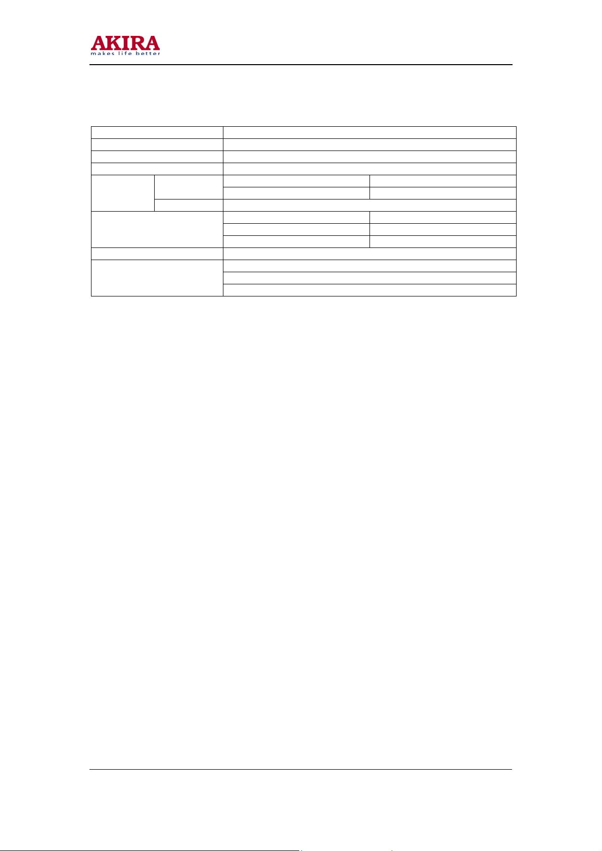
SPECIFICATION
Rated Voltage AC 110V~250V 50Hz/60Hz
Power Consumption 65W
Sound output: 3W×2
Screen size Picture tube 21 inch
System:
Color
Sound D.K / B.G
Channel coverage:
IF 38MHz
External input/output
2
I
C Bus Control
Auto Search
Off/On Timer
Teletext
RF PAL SECAM
AV NTSC
VHF Low channel (VL) =48.25 to 147.25 MHz
VHF high channel (VH) =154.25 to 463.25 MHz
UHF channel (U) =471.25 to 863.25 MHz
Video/Audio (L/R) 1set input at side
YUV & SVHS at rear
AV output at rear
Model No: 21WHS3BN
Version 1.0

5
THE SURVEY
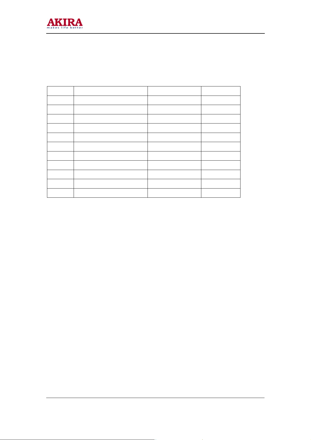
Table 1, the main IC and functions
Number Function IC Remark
1 Power supply KA5Q0765RT N501
2 CPU + SIGNAL PROCESSER TDA9381 N301
3 Field driver LA78040 STV9302A N401
4 Sound processor TDA9859 N122
5 Sound driver AN7522N(stereo) N161
6 AV SWITCH
7 5V Regulator L7805CV N505
8 8V Regulator L7808CV N503
9 Memory AT24C08 N702
10 Photo-coupler HS817B N504
11 IR-receiver HS0038A U701
TC4052BP N801 (Video)
Model No: 21WHS3BN
Version 1.0

6
THE MAIN CHIPS INSTRUCTION
The UOC (“Ultimate One Chip”) TDA9381/61 is adopted in this chassis. This IC is the first available
component that contains the complete control and small signal functionality needed for a TV
application in one device.
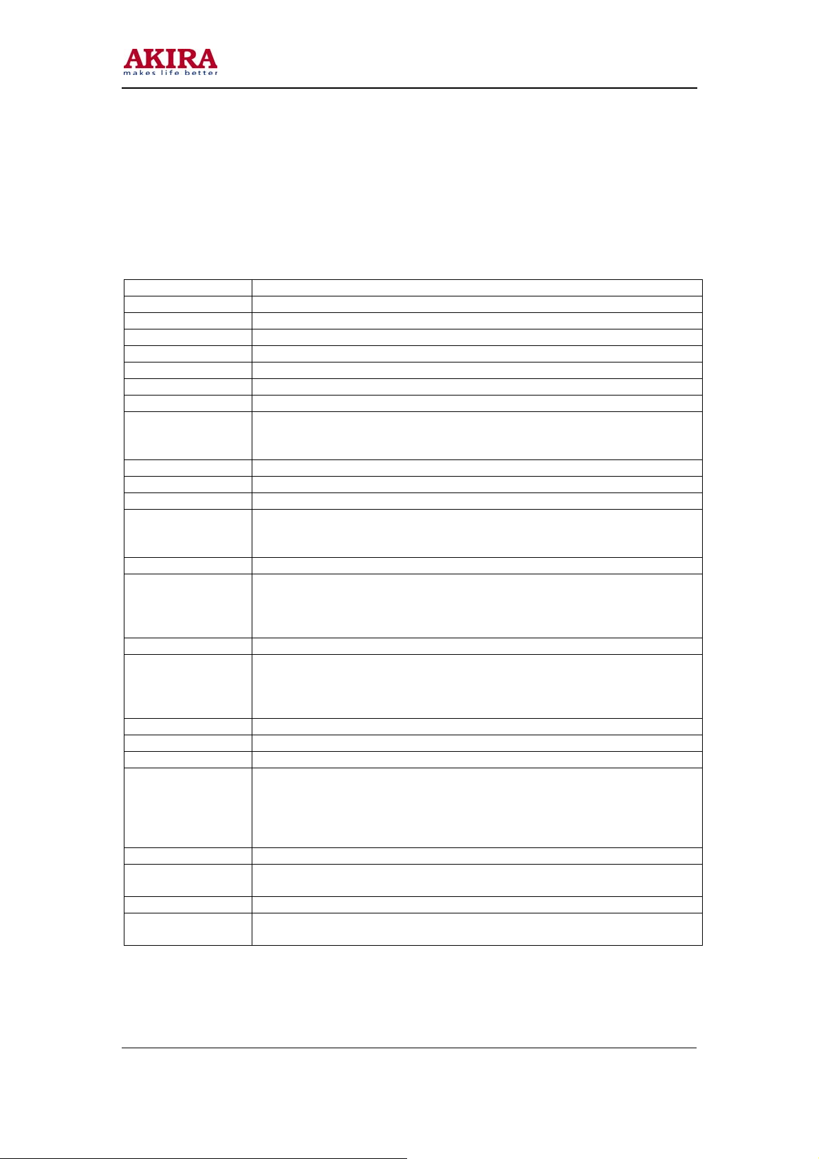
1. The UOC TDA9361/81 pins function description
Pin1: Standby control,“1” is on,“0”is off.
Pin2: SCL.
Pin3: SDA.
Pin4: Tuning PWM output.
Pin5: NTSC SWITCH.
Pin6: Key board input.
Pin7: VOL1, controls the 9 pin of the N101 and supplies DC voltage.
Pin8: Mute control,“1” is mute,“0”is off.
Pin9, Pin12,Pin18,
Pin30, Pin35, Pin41,
Pin55:
Pin10 & Pin11: Band control of the tuner, the two pins needs the pull-up resistance.
Pin13: SECAM PLL, connected with a capacitor.
Pin14: +8V power source supply.
Pin15: Using a capacitor of 220n in series to GND, This pin decouples the internal
Pin16: PHI-2 control loop, this pin requires a capacitor at 2.2nF (C) in series to GND.
Pin17: PHI-1 control loop, the loop filter connected to pin 17 is suitable for various
Pin18: GND
Pin19: Bandgap decoupling, the bandgap circuit provides a very stable and
Pin20: AVL filter, according to the different soft edition.
Pin21, Pin22: Vertical drive output.
Pin23, Pin24: IF input.
Pin25: Reference current, This pin requires a resistor to ground. The optimal
Pin26: Vertical saw tooth, This pin requires a capacitor to ground of 100nF.
Pin27:
Pin28: Audio de-emphasis.
Pin29:
GND.
digital supply voltage of the video processor and minimizes the disturbance to
the sensitive analogue parts.
signal conditions like strong/weak and VCR signal. This is achieved by
switching of the loop filter time constant by changing the PHI-1 output
current.
temperature independent reference voltage. This reference voltage (4.0 V)
ensures optimal performance of the analogue video processor part of the
TDA9381 and is used in almost all functional circuit blocks.
reference current is 100mA which is determined by this resistor. The 100mA
reference current should not be changed because the geometry processor is
optimized for this current. Furthermore the output current of vertical drive and
EW are proportional to this current.
AGC output. This output is used to control (reduce) the tuner gain for strong
RF signals.
Sound decoupling. This pin requires a capacitor connected to ground. The pin
acts as a low pass filter needed for the DC feedback loop.
total 64 pins
:( )
Model No: 21WHS3BN
Version 1.0
 Loading...