

Page 1

21V-R70MM
SERVICE MANUAL
S677421VR70MM
COLOUR TELEVISION
Chassis No. GA4
Chassis No. GA6
MODEL
In the interests of user safety (Required by safety regulations in some countries) the set should be restored to its original
condition and only parts indentical to those specified should be used.
CONTENTS
IMPORTANT SERVICE SAFETY PRECAUTION ................................................................................................... 1-1
LOCATION OF USER’S CONTROL ...................................................................................................................... 2-1
INSTALLATION AND SERVICE INSTRUCTIONS ................................................................................................. 3-1
SERVICE MODE ..................................................................................................................................................... 4-1
ADJUSTMENT METHOD ........................................................................................................................................ 5-1
WAVEFORMS ......................................................................................................................................................... 6-1
CHASSIS LAYOUT ................................................................................................................................................. 7-1
BLOCK DIAGRAM .................................................................................................................................................. 8-1
DESCRIPTION OF SCHEMATIC DIAGRAM .......................................................................................................... 9-1
SCHEMATIC DIAGRAMS ......................................................................................................................................10-1
PRINTED WIRING BOARD ASSEMBLIES ........................................................................................................... 11-1
Parts Guide
21V-R70MM
Page
ELECTRICAL SPECIFICATIONS
POWER INPUT............................AC 110-230 V, 50/60 Hz
POWER RATING .....................................................82W
PICTURE SIZE .............................1,239 cm
CONVERGENCE ............................................. Magnetic
SWEEP DEFLECTION .................................. .. Magnetic
FOCUS ........................................................ Electrostatic
INTERMEDIATE FREQUENCIES
Picture IF Carrier Frequency ...................... 45.75 MHz
Sound IF Carrier Frequency ...................... 41.25 MHz
Color Sub-Carrier Frequency ......................42.17 MHz
(Nominal)
AUDIO POWER
OUTPUT RATING... ...................... 3.0 W(RMS) x 1pc
2
(192sq inch)
SPEAKER
SIZE ........................................................ 2” X 3.5”, 1pc
VOICE COIL IMPEDANCE .................16 ohm at 400 Hz
ANTENNA INPUT IMPEDANCE
VHF/UHF ........................................75 ohm Unbalanced
TUNING RANGES
VHF-Channels ................................................. 2 thru 13
UHF-Channels ................................................14 thru 69
CATV Channels ............................................. 1 thru 125
(EIA, Channel Plan U.S.A.)
Specifications are subject to change without
prior notice.
SHARP CORPORATION
This document has been published to be used for after
sales service only.
The contents are subject to change without notice.
Page 2

21V-R70MM
TV21V-R70MMService Manual21V-R70MMMarketE
CHAPTER 1. IMPORTANT SERVICE SAFETY PRECAUTION
IMPORTANT SERVICE SAFETY PRECAUTION
Service work should be performed only by qualified service technicians who are
thoroughly familiar with all safety checks and the servicing guidelines which follow:
WARNING
1. For continued safety, no modification of any circuit
should be attempted.
2. Disconnect AC power before servicing.
3. Semiconductor heat sinks are potential shock
hazards when the chassis is operating.
4. The chassis in this receiver has two ground systems
which are separated by insulating material. The nonisolated (hot) ground system is for the B+ voltage
regulator circuit and the horizontal output circuit. The
isolated ground system is for the low B+ DC voltages
and the secondary circuit of the high voltage
transformer.
To prevent electrical shock use an isolation
transformer between the line cord and power
receptacle, when servicing this chassis.
SERVICING OF HIGH VOLTAGE SYSTEM
AND PICTURE TUBE
When servicing the high voltage system,
remove the static charge by connecting a
10k ohm resistor in series with an insulated
wire (such as a test probe) between the picture tube ground and the anode lead. (AC
line cord should be disconnected from AC
outlet.)
1. Picture tube in this receiver employs integral
implosion protection.
2. Replace with tube of the same type number for
continued safety.
3. Do not lift picture tube by the neck.
4. Handle the picture tube only when wearing
shatterproof goggles and after discharging the high
voltage anode completely.
X-RADIATION AND HIGH VOLTAGE LIMITS
1. Be sure all service personnel are aware of the
procedures and instructions covering X-radiation.
The only potential source of X-ray in current solid
state TV receivers is the picture tube. However, the
picture tube does not emit measurable X-Ray
radiation, if the high voltage is as specified in the
"High Voltage Check" instructions.
It is only when high voltage is excessive that Xradiation is capable of penetrating the shell of the
picture tube including the lead in the glass material.
The important precaution is to keep the high voltage
below the maximum level specified.
2. It is essential that servicemen have available at all
times an accurate high voltage meter.
The calibration of this meter should be checked
periodically.
3. High voltage should always be kept at the rated value
−no higher. Operation at higher voltages may cause
a failure of the picture tube or high voltage circuitry
and;also, under certain conditions, may produce
radiation in exceeding of desirable levels.
4. When the high voltage regulator is operating properly
there is no possibility of an X-radiation problem.
Every time a color chassis is serviced, the brightness
should be tested while monitoring the high voltage
with a meter to be certain that the high voltage does
not exceed the specified value and that it is regulating
correctly.
5. Do not use a picture tube other than that specified
or make unrecommended circuit modifications to the
high voltage circuitry.
6. When trouble shooting and taking test
measurements on a receiver with excessive high
voltage, avoid being unnecessarily close to the
receiver.
Do not operate the receiver longer than is necessary
to locate the cause of excessive voltage.
1 – 1
Page 3
IMPORTANT SERVICE SAFETY PRECAUTION
(Continued)
BEFORE RETURNING THE RECEIVER
(Fire & Shock Hazard)
Before returning the receiver to the user, perform
the following safety checks.
1. Inspect all lead dress to make certain that leads are
not pinched or that hardware is not lodged between
the chassis and other metal parts in the receiver.
2. Inspect all protective devices such as non-metallic
control knobs, insulating materials, cabinet backs,
adjustment and compartment covers or shields,
isolation resistor-capacity networks, mechanical
insulators, etc.
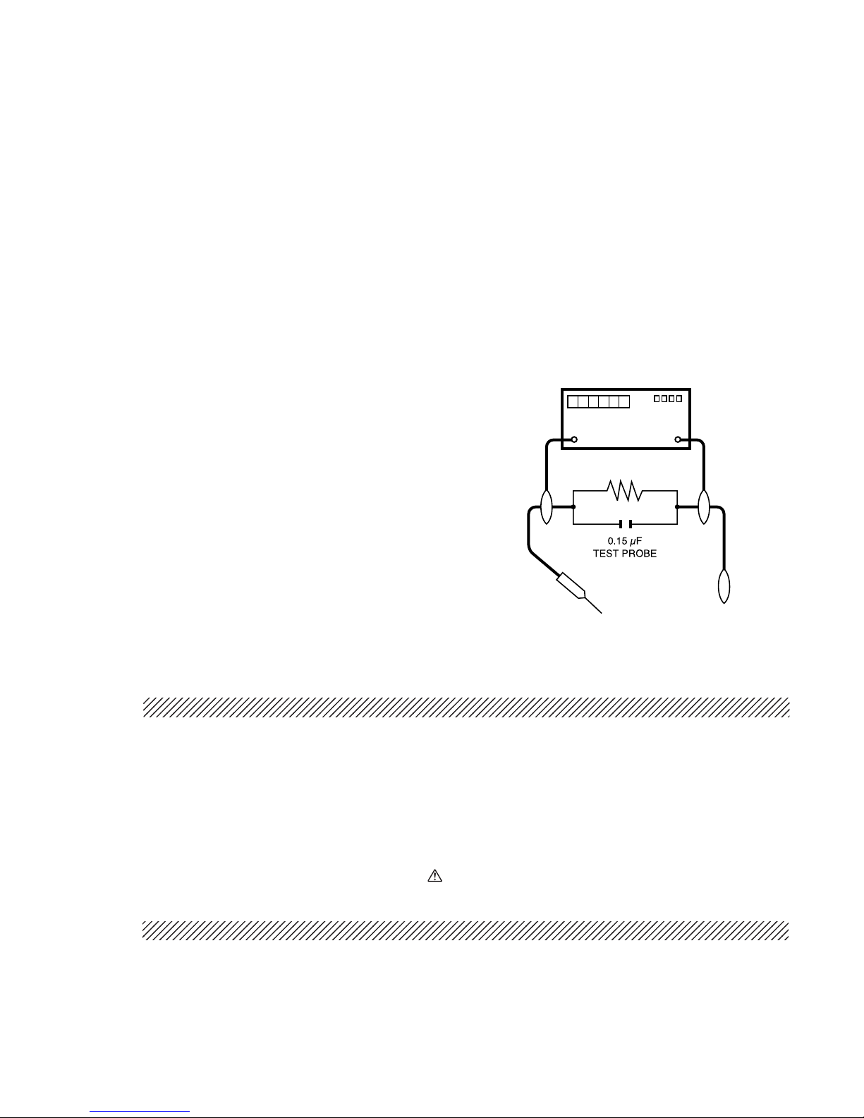
3. To be sure that no shock hazard exists, check for
leakage current in the following manner.
•
Plug the AC cord directly into a 110~230 volt AC
outlet, (Do not use an isolation transformer for this
test).
•
Using two clip leads, connect a 1.5k ohm, 10 watt
resistor paralleled by a 0.15µF capacitor in series
with all exposed metal cabinet parts and a known
earth ground, such as electrical conduit or electrical
ground connected to earth ground.
•
Use an AC voltmeter having with 5000 ohm per volt,
or higher, sensitivity to measure the AC voltage drop
across the resistor.
21V-R70MM
•
Connect the resistor connection to all exposed metal
parts having a return to the chassis (antenna, metal
cabinet, screw heads, knobs and control shafts,
escutcheon, etc.) and measure the AC voltage drop
across the resistor.
AII checks must be repeated with the AC line cord
plug connection reversed. (If necessary, a nonpolarized adapter plug must be used only for the
purpose of completing these check.)
Any current measured must not exceed 0.5 milliamp.
Any measurements not within the limits outlined
above indicate of a potential shock hazard and
corrective action must be taken before returning the
instrument to the customer.
DVM
AC SCALE
1.5k ohm
10W
SAFETY NOTICE
Many electr ical and mechanical parts in television
receivers have special safety-related characteristics.
These characteristics are often not evident from visual
inspection, nor can protection afforded by them be
necessarily increased by using replacement components
rated for higher voltage, wattage, etc.
Replacement parts which have these special safety
characteristics are identified in this manual; electrical
components having such features are identified by "
and shaded areas in the Replacement Parts Lists and
Schematic Diagrams.
TO EXPOSED
METAL PARTS
For continued protection, replacement parts must be
identical to those used in the or iginal circuit. The use of
substitute replacement parts which do not have the same
safety characteristics as the factory recommended
replacement parts shown in this service manual, may
create shock, fire, X-radiation or other hazards.
"
CONNECT TO
KNOWN EARTH
GROUND
1 – 2
Page 4

21V-R70MM
TV21V-R70MMService Manual21V-R70MMMarketE
CHAPTER 2. LOCATION OF USER'S CONTROL
[1] LOCATION OF USER'S CONTROL
2 – 1
Page 5

21V-R70MM
TV21V-R70MMService Manual21V-R70MMMarketE
CHAPTER 3. INSTALLATION AND SERVICE INSTRUCTIONS
INSTALLATION AND SERVICE INSTRUCTIONS
Note: (1) When performing any adjustments to resistor controls and transformers use non-metallic
screwdrivers or TV alignment tools.
(2) Before performing adjustments, the TV set must be on at least 15 minutes.
CIRCUIT PROTECTION
The receiver is protected by a 3.15A fuse (F701),
mounted on PWB-A, wired into one side of the AC
line input.
X-RADIATION PROTECTOR CIRCUIT TEST
After service has been performed on the horizontal
deflection system, high voltage system, B+ system,
test the X-Radiation protection circuit to ascertain
proper operation as follows:
1. Apply 110~230V AC using a variac transformer for
accurate input voltage.
2. Allow for warm up and adjust all customer controls
for normal picture and sound.
3. Receive a good local channel.
4. Connect a digital voltmeter to P603 pin3 and make
sure that the voltmeter reads 20 ±1.1V.
5. Apply external 27V DC at P603 pin3 by using an
external DC supply, TV must be shut off.
6. To reset the protector, unplug the AC cord and make
a shor t circuit between P603 pin1 and P603 pin2.
Now make sure that normal picture appears on the
screen.
7. If the operation of the horizontal oscillator does not
stop in step 5, the circuit must be repaired before the
set is returned to the customer.
HIGH VOLTAGE CHECK
High voltage is not adjustable but must be checked
to verify that the receiver is operating within safe
and efficient design limitations as specified checks
should be as follows:
1. Connect an accurate high voltage meter between
ground and anode of picture tube.
2. Operate receiver for at least 15 minutes at 110~230V
AC line voltage, with a strong air signal or a properly
tuned in test signal.
3. Enter the service mode and set Y-mute ON by using
Service R/C.
4. The voltage should be approximately 28.7kV (at zero
beam).
If a correct reading cannot be obtained, check circuitry
for malfunctioning components. After the voltage test,
make Y-mute off to the normal mode.
3 – 1
Page 6
TV21V-R70MMService Manual21V-R70MMMarketE
CHAPTER 4. SERVICE MODE
Service Mode Overview
1. Service mode is entered by SERVICE key input or CH-UP +VOL-DOWN input during reset.
2. Service mode is cleared by entering SERVICE key command during service mode.
3. If key input port (SERVICE) input is LOW, then it is in service mode.
4. During key input port (SERVICE) input is LOW, clearing service mode by key input SERVICE is disabled.
5. Service mode can be switched to 4 modes as follows by key input MENU;
Adjustment mode
21V-R70MM
SERVICE MODE
Setting mode
Check mode
Option mode
6. AFT processing is disabled during service mode. PLL setting data is set to fo data.
7. All user data are set to default during service mode. FAO and SPEAKER user settings are off and on respectively
in service mode. Energy Save is off.
8. Sleep timer, View timer, on timer and off timer are inactivated in Service mode.
9. Sound is muting in service mode except at Adjustment Items V20, M01, M03, M04, M05, and M06.
First mode of service mode when SERVICE key is
pressed.
First mode of service mode when local key
CH-UP + VOL-DOWN is pressed after MCU reset.
4 – 1
Page 7

21V-R70MM
Adjustment Mode Items
No. Item Name IC Register Range Default
V01 SUB-PICTURE 1 Chip CONTRAST 0~127 127
V02 SUB-TINT 1 Chip TINT 0~127 64
V03 SUB-COLOR 1 Chip COLOR 0~127 64
V04 SUB-BRIGHT 1 Chip BRIGHT 0~255 128
V05 SUB-SHARP 1 Chip VIDEO-TONE 0~63 32
V06 V-SHIFT 1 Chip V-SHIFT 0~7 4
V07 H-SHIFT 1 Chip H-PHASE 0~31 16
V08 RF-AGC 1 Chip RF-DELAY 0~127 127
V09 V-SIZE 1 Chip V-SIZE 0~63 32
V10 PIF-VCO 1 Chip VIF-VCO 0~63 32
V11 R-CUTOFF 1 Chip R-CUTOFF 0~255 127
V12 G-CUTOFF 1 Chip G-CUTOFF 0~255 127
V13 B-CUTOFF 1 Chip B-CUTOFF 0~255 127
V14 R-DRIVE 1 Chip R-DRIVE 0~127 64
V15 B-DRIVE 1 Chip B-DRIVE 0~127 64
V16 SUB-COLOR(YUV) 1 Chip COLOR 0~127 64
V17 SUB-TINT(YUV) 1 Chip BASEBAND-TINT 0~127 64
V18 CC-POS MICON CC-POS 0~255 32
V19 SCREEN CUT OFF 1 Chip CUT OFF 0~2 0
V20 SUB-VOL 1 Chip A-ATT 0~127 127
V21 H-VCO 1 Chip H-VCO 0~7 4
M01 MTS-ATT MTS ATT (MTS) 0~15 10
M02 MTS-VCO MTS VCO (MTS) 0~63 32
M03 MTS-FILTER MTS FILTER (MTS) 0~63 28
M04 MTS-WIDEBAND MTS WIDEBAND (MTS) 0~63 27
M05 MTS-SPECTRAL MTS SPECTRAL (MTS) 0~63 32
M06 SUB-VOL MTS VOL (MTS) 0~63 63
4 – 2
Page 8

21V-R70MM
SELF ADJUSTMENT
H-VCO
1. When there is H-VCO self-adjustment key input for adjustment item H-VCO, self-adjustment is performed.
2. H-FREE(1chip) is set to 1.
3. H-OUT is set by intelligent monitor output.
4. IM input is set as TIM input.
5. H-VCO(1chip) data is changed so that the number of input pulse is 125 inside 8ms interval.
6. When adjustment completed, OSD display and H-VCO self-adjustment status data of EEPROM are updated.
7. H-FREE(1chip), intelligent monitor output and IM input mode are recovered.
RF-AGC
1. When there is RF-AGC self-adjustment key input for adjustment item RF-AGC, self-adjustment is performed.
2. AGC-OUT is set by intelligent monitor output.
3. IM input is set as AD input.
4. By decreasing RF-AGC (1chip) data from current RF-AGC adjustment value to 0, AFT input voltage becomes the
maximum setting value.
5. Increase RF-AGC(1chip) data, when AFT input voltage is at (max. 0.3V) point, adjustment is completed.
6. When adjustment completed, OSD display and RF-AGC self-adjustment status data of EEPROM are updated.
7. Intelligent monitor output and IM input mode are recovered.
PIF-VCO
1. When there is PIF-VCO self-adjustment key input for adjustment item PIF-VCO, self-adjustment is performed.
2. VIF-DEF(1chip) is set to 1.
3. AFC is set by intelligent monitor output.
4. IM input is set as AD input.
5. VIF-VCO(1chip) data is changed so that input voltage becomes 2.5V.
6. When adjustment completed, OSD display and PIF-VCO self-adjustment status data of EEPROM are updated.
7. VIF-DEF(1chip), intelligent monitor output and IM input mode are recovered.
4 – 3
Page 9

21V-R70MM
Setting Mode Items
No. Item Name IC Register Range Default
F01 VIDEO TONE -GAIN (TV) 1 Chips V-TONE 0/1 0
F02 VIDEO TONE -GAIN (AV) 1 Chips V-TONE 0/1 0
F03
VIDEO TONE -GAIN (S-AV)
F04 VIDEO TONE -GAIN(YUV) 1 Chips V-TONE 0/1 0
F05 ABCL 1 Chips ABCL 0/1 0
F06 BS 1 Chips BS-OFF 0/1 0
F07 ABCL-G 1 Chips ABCL-G 0/1 0
F08 SHP-AV OFFSET VIDEO-TONE(OFFSET) -16~+16 0
F09 SHP-SAV OFFSET VIDEO-TONE(OFFSET) -16~+16 0
F10 SHP-YUV OFFSET VIDEO-TONE(OFFSET) -16~+16 0
F11 RGB-CLIP 1 Chips EXTRGB-CLIP 0/1 0
F12 E-SAVE OFFSET CONTRAST(OFFSET) 0~63 30
F13 FAO-VOL 1 Chips A-ATT 0~127 120
F14 PIF-G 1 Chips VIF-GAIN 0~7 4
F15 Y-DELAY(TV) 1 Chips Y-DELAY 0~7 0
F16 Y-DELAY(AV) 1 Chips Y-DELAY 0~7 0
F17 Y-DELAY(SAV) 1 Chips Y-DELAY 0~7 0
F18 Y-DELAY(YUV) 1 Chips Y-DELAY 0~7 0
F19 TINT-AV OFFSET TINT(OFFSET) -32~+32 0
F20 TINT-SAV OFFSET TINT(OFFSET) -32~+32 0
F21 COL-AV OFFSET COLOR(OFFSET) -32~+32 0
F22 COL-SAV OFFSET COLOR(OFFSET) -32~+32 0
F23 R-DRI(R2) OFFSET R-DRI(OFFSET) -32~+32 0
F24 R-DRI( R) OFFSET R-DRI(OFFSET) -32~+32 0
F25 R-DRI(B) OFFSET R-DRI(OFFSET) -32~+32 0
F26 B-DRI(R2) OFFSET B-DRI(OFFSET) -32~+32 0
F27 B-DRI( R) OFFSET B-DRI(OFFSET) -32~+32 0
F28 B-DRI(B) OFFSET B-DRI(OFFSET) -32~+32 0
F29 V-FREE 1 Chips V-FREE 0/1 0
F30 GAMMA 1 Chips GAMMA 0~3 0
F31 TRAP(TV) 1 Chips TRAP-FINE 0~3 2
F32 TRAP(AV) 1 Chips TRAP-FINE 0~3 2
F33 H-FREE 1 Chips H-FREE 0/1 0
F34 1W(TV) 1 Chips V.WINDOW 0/1 0
F35 1W(AV) 1 Chips V.WINDOW 0/1 0
F36 YLPF 1 Chips YSW-LPF 0/1 1
F37 BS-D 1 Chips BS-DISCHARGE 0~3 0
F38 BS-C 1 Chips BS-CHARGE 0~3 0
F39 SL(TV) 1 Chips S-SLICE DOWN 0~3 0
F40 SL(AV) 1 Chips S-SLICE DOWN 0~3 0
F41 SL(SAV) 1 Chips S-SLICE DOWN 0~3 0
F42 SL(YUV) 1 Chips S-SLICE DOWN 0~3 0
F43 AFC2 1 Chips AFC2-G 0/1 0
F44 VD(TV) 1 Chips VSYNC-DET 0/1 0
F45 VD(AV) 1 Chips VSYNC-DET 0/1 0
F46 AS(TV) 1 Chips AUTO-SLICE 0/1 0
F47 AS(AV) 1 Chips AUTO-SLICE 0/1 0
F48 AS(SAV) 1 Chips AUTO-SLICE 0/1 0
F49 AS(YUV) 1 Chips AUTO-SLICE 0/1 0
F50 FBP(TV) 1 Chips FBP VTH 0/1 0
F51 FBP(AV) 1 Chips FBP VTH 0/1 0
F52 FBP(SAV) 1 Chips FBP VTH 0/1 0
F53 FBP(YUV) 1 Chips FBP VTH 0/1 0
F54 C.CLIP LEVEL 1 Chips C.CLIP LEVEL 0/1 0
1 Chips V-TONE 0/1 0
4 – 4
Page 10
Setting Mode Items (Continued)
No. Item Name IC Register Range Default
F55 PSW MTS PSW 0/1 0
F56 FAO-VOL MTS VOL 0~63 60
F57 CP PLL CHARGE PUMP 0/1 0
F58 CC LEVEL MICON CC LEVEL 0/1 0
F59 OSD POS MICON OSD POS 0/1 0
F60 OFFSET-ADJ-COL 1 Chips COLOR -32~+32 0
F61 OFFSET-ADJ-TINT 1 Chips TINT -32~+32 0
F62 OFFSET-ADJ-TINT-YUV 1 Chips BASEBAND-TINT -32~+32 0
F63 TIMER4-LOW SPEED 1 Chips TIMER4 VALUE 0~225 50
F64 TIMER4-HIGH SPEED 1 Chips TIMER4 VALUE 0~225 125
F65 R-CUT-YUV 1 Chips R-CUT(OFFSET) -63~+63 0
F66 G-CUT-YUV 1 Chips G-CUT(OFFSET) -63~+63 0
F67 B-CUT-YUV 1 Chips B-CUT(OFFSET) -63~+63 0
F68 R-DRI-YUV 1 Chips R-DRI(OFFSET) -63~+63 0
F69 B-DRI-YUV 1 Chips B-DRI(OFFSET) -63~+63 0
F70 CLOCK-ADJ 1 Chips 0~25 25
21V-R70MM
4 – 5
Page 11

21V-R70MM
Option Mode Items
OPTION FUNCTION
No
001 DEMO Without DEMO With DEMO 1
002 DOWNLOAD Without V-CHIP OP With V-CHIP OP 0
003 V-CHIP Without V-CHIP With V-CHIP 0
004 SPEAKER Without SPEAKER With SPEAKER 1
005 FAO Without FAO With FAO 1
006 P.PREF Without P.REF With P.REF 1
007 UNIV+ Without UNIV+ With UNIV+ 1
008 VIEW TIMER Without VIEW TIMER With VIEW TIMER 1
009 EZ-SETUP EZ-SETUP AUTO PRESET 0
010 PON-CH Without POWER-ON With POWER-ON 0
011 FAV-COL FAV-COL COL-TEMP 1
012 COMPONENT Without COMPONENT With COMPONENT 1
013 AV Without AV With AV 1
014 AV2 AV1 system AV2 system 1
015 MTS Without MTS With MTS 1
016 TONE-CTRL Without S-ADJ With S-ADJ 1
017 AUTO-OFF Without AUTO-OFF With AUTO-OFF 1
018 INIT-LANG ENGLISH SPANISH 1
019 SETUP-FLAG NO SET UP AUTO SET UP 1
020 AV-FR
021 AV3/S-IN Without AV3/S-IN With AV3/S-IN 0
022 COMB Without COMB With COMB 0
023 AUTO-INPUT Without AUTO-INPUT With AUTO-INPUT 1
024 CLOCK Without CLOCK With CLOCK 1
025 LED SEMEX MODEL SPC MODEL 0
026 FLAT Not FLAT MODEL FLAT MODEL 1
027 BASS BOOST Without BASS BOOST With BASS BOOST 0
028 DSE Without DSE With DSE 0
029 SRS Without SRS With SRS 0
030 WHITE-OUT Without WHITE-OUT With WHITE-OUT 1
"0"=NO AV "1"=REAR "2"=FRONT "3"=REAR & FRONT
01
Default Data
3
Check Mode
Micron mask version, software version and ROM correction function status are displayed in check mode.
4 – 6
Page 12
TV21V-R70MMService Manual21V-R70MMMarketE
CHAPTER 5. ADJUSTMENT METHOD
Memory Map Data
Caution: to get into the s ervice mode, one of the ways is press direct key for service items.
There is three s tage of S ervice Mode data
First stage data from V01 ~ M06
to go into second stage of service mode data, press MENU key
S econd stage data from F01 ~ F70
to go into third s ta ge o f s e rv ic e mode da ta , pre s s ME N U ke y
Third stage data from O01 ~ O30
Below is the contents of these da ta
First Stage
Data
V01 C O NT R AS T 0~127 127 127
V02 TINT 0~127 64 54
V03 COLOR 0~127 64 35
V04 B R IGHT 0~255 128 127
V05 VIDEO-TONE 0~63 43 45
V06 V-SHIFT 0~7 4 2
V07 H-P HA S E 0~31 16 11
V08 R F -DE LAY 0~127 127 127
V09 V-SIZE 0~63 32 40
V10 VIF -V C O 0~63 32 32
V11 R -C U T OF F 0~255 127 127
V12 G -C U T OF F 0~255 127 127
V13 B -C U T OF F 0~255 127 127
V14 R -DR IVE 0~127 64 64
V15 B -DR IVE 0~127 64 64
V16 COLOR 0~127 64 64
V17 BAS E B AN D-TINT 0~127 64 64
V18 C C -P O S 0~255 32 32
V19 CUTOFF 0~2 0 0
V20 A-ATT 0~127 127 127
V21 H-VC O 0~7 4 4
M01 ATT (MTS ) 0~15 10 10
M02 V CO (MTS ) 0~63 32 32
M03 F ILT E R (MTS ) 0~63 28 28
M04 W IDE B AND (MTS ) 0~6 3 27 27
M05 S P E C TR AL (MTS ) 0~63 32 32
M06 V OL (MT S ) 0~6 3 63 63
Service Mode
SUB-PICTURE
SUB-TINT
SUB-COLOR
SUB-BRIGHT
SUB-SHARP
V-SHIFT
H-SHIFT
RF-AGC
V-SIZE
PIF-VCO
R-CUTOFF
G-CUTOFF
B-CUTOFF
R-DRIVE
B-DR IVE
SUB-COLOR(YUV)
SUB-TINT(YUV)
CC-POS
SCREEN CUTOFF
SUB-VOL
H-VCO
MT S -ATT
MT S -V CO
MT S -F ILT E R
MT S -W IDE B AN D
MT S -S P E C T R AL
SUB-VOL
Function Range
Default
Data
21V-R70MM
S e tting
Data
Auto Adjustment Ite m
1. H-V C O
2. R F-AG C
3. P IF -VC O
5 – 1
Page 13
21V-R70MM
T
T
T
T
T
T
T
Second Stage
Data S e rvic e Mode F unc tion R ange
F01 V-TONE 0/1 0 0
F02 V-TONE 0/1 0 0
F03 V-TONE 0/1 0 0
F04 V-TONE 0/1 0 0
F05 ABCL 0/1 0 0
F06 BS-OFF 0/1 0 0
F07 ABCL-G 0/1 0 0
F08 VIDEO-TONE(OFFSET) -16~+16 0 0
F09 VIDEO-TONE(OFFSET) -16~+16 0 0
F10 VIDEO-TONE(OFFSET) -16~+16 0 0
F11 EXTRGB-CLIP 0/1 0 0
F12 C ONTR AS T(OFFS E T) 0~63 30 30
F13 A-ATT 0~127 120 120
F14 VIF-GAIN 0~7 4 4
F15 Y-DELAY 0~7 0 5
F16 Y-DELAY 0~7 0 2
F17 Y-DELAY 0~7 0 0
F18 Y-DELAY 0~7 0 0
F19
F20
F21 COLOR(OFFSE T) -32~+32 0 +2
F22 COLOR(OFFSE T) -32~+32 0 0
F23 R -DR I(OF F S E T) -32~+32 0 +8
F24 R -DR I(OF F S E T) -32~+32 0 +3
F25 R -DR I(OF F S E T) -32~+32 0 -2
F26 B-DR I(OFF S E T) -32~+32 0 -18
F27 B-DR I(OFF S E T) -32~+32 0 -8
F28 R -DR I(OF F S E T) -32~+32 0 +6
F29 V-FRE E 0/1 0 0
F30 GAMMA 0~3 0 1
F31
F32
F33 H-FR EE 0/1 0 0
F34 V.WINDOW 0/1 0 0
F35 V.WINDOW 0/1 0 1
F36 YSW-LPF 0/1 1 1
F37 BS-DISCHARGE 0~3 0 0
F38 BS-CHARGE 0~3 0 0
F39 S-SLIC E DOWN 0~3 0 1
F40 S-SLIC E DOWN 0~3 0 1
F41 S-SLIC E DOWN 0~3 0 0
F42 S-SLIC E DOWN 0~3 0 0
F43 AFC2-G 0/1 0 0
F44 VSYNC-DET 0/1 0 1
F45 VSYNC-DET 0/1 0 0
F46 AUTO-SLIC E 0/1 0 1
F47 AUTO-SLIC E 0/1 0 1
F48 AUTO-SLIC E 0/1 0 0
F49 AUTO-SLIC E 0/1 0 0
F50 FBP VTH 0/1 0 0
F51 FBP VTH 0/1 0 0
F52 FBP VTH 0/1 0 0
F53 FBP VTH 0/1 0 0
F54 C.CLIP LEVEL 0/1 0 0
F55 PSW 0/1 0 0
F56 VO L 0~63 60 58
F57 CHARG E PUMP 0/1 0 1
F58 CC LEVEL 0~31 0 0
F59 OSD POS 0/1 0 0
F60 COLOR -32~+32 0 +10
F61
F62 BAS E BAND-TINT -32~+32 0 -12
F63
F64
VIDEO-TONE-GAIN (TV)
VIDEO-TONE-GAIN (AV)
VIDE O -T O NE -G AIN (S-AV )
VIDEO-TONE-GAIN (YUV)
ABC L
BS
ABC L-G
SHP-AV
SHP-SAV
SHP-YUV
RGB-CLIP
E-SAVE
FAO-VOL
PIF-G
Y-DELAY(TV)
Y-DELAY(AV)
Y-DELAY(SAV)
Y-DELAY(YUV)
TINT-AV
TINT-SAV
COL-AV
COL-S AV
R-DRI(R2)
R-DRI( R)
R-DRI(B)
B-DRI(R2)
B-DRI( R )
R-DRI(B)
V-FREE
G AMMA
TRAP (TV)
TRAP (AV)
H-FR E E
1W (T V)
1W (AV )
YLPF
BS-D
BS-C
SL(TV)
SL(AV)
SL(SAV)
SL(YUV)
AFC 2
VD(TV)
VD(AV)
AS (T V )
AS (AV )
AS (S AV )
AS (Y UV)
FBP(TV)
FBP(AV)
FBP(SAV)
FBP(YUV)
C.CLIP LEVEL
PSW
FAO-VOL
CP
CC LEVEL
OSD POS
OFFSE T-ADJ-COL
OF FS ET -ADJ -T INT
OFFSE T-ADJ-TINT-YUV
TIMER4-LOW SPEED
TIMER4-HIGH SPEED
INT(OF F S E T) -32~+32 0 -2
INT(OF F S E T) -32~+32 0 0
RAP-FINE 0~3 2 2
RAP-FINE 0~3 2 2
INT -32~+32 0 +8
IMER 4 VAL UE 0~255 50 50
IMER 4 VAL UE 0~255 125 125
Default
Data
Setting
Data
5 – 2
Page 14

21V-R70MM
F 6 5 R -C U T(O F FS E T) -63~+63 0 0
F66 G-CUT(OFFSE T) -63~+63 0 +36
F67 B-CUT(OFFSE T) -63~+63 0 +2
F68 R -DR I(OFF S E T ) -63~+63 0 0
F69 B-DR I(OFF S E T ) -63~+63 0 0
F70 0~25 25 25
R-CUT-YUV
G-CUT-YUV
B-CUT-YUV
R-DRI-YUV
B-DR I-YUV
CLOCK-ADJ
Third stage
Data OPTION F UNCTION DATA = " 0"
O01 DEMO DISABLE ENABLE 1 1
O02 V -C HIP OP DIS AB LE E NAB L E 0 0
O03 V -C HIP DIS AB LE E N AB L E 0 0
O04 SP E AKE R DISABL E E NABLE 1 0
O05 FAO DISABLE E NABL E 1 0
O06 P.REF DIS ABLE ENABLE 1 0
O07 UNIV+ DIS ABLE ENABLE 1 0
O 08 VIE W TIME R DIS AB LE E NAB L E 1 1
O09 EZ-SE TUP AUTO PR E S E T 0 0
O10 POW E R -ON DISABLE ENABLE 0 1
O11 FAV-COL C OL-TEMP 1 1
O12 CO MPONE NT DIS ABL E ENAB LE 1 0
O13 AV DISABLE E NABLE 1 1
O14 AV1 AV2 1 0
O15 MTS DISABLE E NABLE 1 0
O16 S-ADJ DISABLE E NABLE 1 1
O17 AUTO-OFF DIS ABLE E NABLE 1 1
O18 ENGLISH SPANISH 1 1
O19 NO S E T UP AUTO S E T UP 1 0
O20 31
O21 AV3/S -IN DISAB LE E NABLE 0 0
O22 COMB DISAB LE E NABLE 0 0
O23 AUT O-INP UT DISAB L E E NABL E 1 0
O24 CLOC K DISAB LE E NABLE 1 0
O25 SEMEX MODEL SPC MODEL 0 1
O26 F L AT DIS AB L E E NABL E 1 0
O27 B AS S BO OS T DIS AB L E E NAB LE 0 0
O28 DSE DIS ABLE E NABLE 0 0
O29 SR S DISAB LE E NABLE 0 0
O30 WHITE-OUT DISABLE ENABLE 1 0
DE MO
DOW NL OAD
V-CHIP
SPEAKER
FAO
P.PRE F
UNIV+
VIEW TIMER
EZ-SETUP
*PON-CH
FAV-COL
COMPONENT
AV
AV2
MT S
TONE -C TR L
AUTO -OF F
INIT -L ANG UAG E
SETUP-FLAG
AV-F R
AV3/S -IN
COMB
AUTO -INPU T
CLOCK
LE D
FLAT
BASS BOOST
DS E
SRS
WHITE-OUT
"0"=NO AV "1"=R E AR "2 "=FR ON T "3 "=R EA R & F R O NT
DATA =" 1"
Default
Data
S e tting
Data
*POWERONBYCH-UP/DOWNKEY.
5 – 3
Page 15

21V-R70MM
MOD E L N AME
ADJU S T ME N T
ITE M
ADJU S T ME N T
POSITION
21V-R 70MM
OPT ION S E T UP
STEP RANGE REFER AS BELOW
CONTROL
PRE-ADJUST
REQUIREMENT
CONTENT
INP U T
C O ND IT ION
OUTPUT
21V-R 70MM
OSD C HEC KING
BUS OPTION
FUNCTION
FOR THIRD STAGE SER VICE DATA
O01 O 02 O03 O04 O05 O 06 O07 O08 O09 O10
DEMO DOWNLOAD V-CHIP SP FAO P.PR E F UNIV+ VIEW EZ PON-CH
ADJ US T ME NT 21V-R 70MM 1 0 0 0 0 0 0 1 0 1
PROCEDURE
DE F
"0"=DISABLE
"1"=ENABLE
009 --> "0"= E Z -S E TU P "1"= AUT O P R E S E T
BUS OPTION
FUNCTION
FOR THIRD STAGE SER VICE DATA
O11 O12 O13 O14 O15 O16 O17 O18 O19 O20
FAV-COL COMP AV AV2 MTS T ONE AUTO
Init-LANG
SETUP AV-FR
21V-R 70MM 1 0 1 0 0 1 1 1 0 1
FUNCTION
O21 O 22 O23 O24 O25 O 26 O27 O28 O29 O30
AV3 COMB A-IN CLOCK LED FLAT BASS DSE S R S WHITE
21V-R 70MM 0 0 0 0 1 0 0 0 0 0
HISTOR Y
OF RE V ISION
DE F O11 --> "0" =F AV -C O L "1"= C O L -T E MP
O18--> "0"= E N G L IS H "1" = S P AN IS H
O19--> "0"= NO S E T UP "1" = AUTO S E T UP
O20 --> "0"=NO AV "1"=R E A R "2"=F R O NT "3"=R E AR &F R ONT
SYMBOL
REVISED CONTENT .
5 – 4
Page 16

21V-R70MM
MOD E L N AME
ADJU S T ME N T
ITE M
ADJU S T ME N T
POSITION
CONTROL
PRE-ADJUST
REQUIREMENT
CONTENT
INP U T
C O ND IT ION
OUTPUT
ADJU S T ME N T
PROCEDURE
21V-R 70MM
BUS SET UP
STEP RANGE R EFER AS BELOW
21V-R 70MM
OSD C HEC KING
DATA S ETUP FOR FIRST AND SECOND STAGE S ERVICE DATA
FUNCTION
21V-R 70MM
FUNCTION
FUNCTION
21V-R 70MM
V05 F15 F 16 F19 F21 F 23 F24 F25 F26 F 27
S H AR P Y -D L .T V Y -DL. AV T INT -AV C OL -AV R -D( R 2 ) R -D ( R ) R -D(B ) B-D ( R 2 ) B-D(R )
-2
F28
B-D(B)
+6
F60 F61 F62
C-OF TINT-OF
F35
F30
GAMMA
F39F40F44F46F47F56F57
1W(AV) SL (TV) S L(AV) VD(TV) AS (TV) AS(AV)
11
1
111
F66
TI-YU V G -C -YU V B -C-Y UV
-12 +36
F67 F36
YLPF
+2 1+10 +8
DE F
-2 -18 -82+8+345 5 2
FAO-VOL
CP
1
58121V-R 70MM
HISTOR Y
OF RE V ISION
SYMBOL
REVISED CONTENT .
5 – 5
Page 17

21V-R70MM
MOD E L N AME
ADJU S T ME N T
ITE M
ADJU S T ME N T
POSITION
CONTROL
PRE -ADJUST
REQUIREMENT
CONTENT
INP U T
C O ND IT ION
OUTPUT
ADJUS T ME NT
PROCEDURE
21V-R 70MM
H-POS ITION
STEP RANGEV07
I2C B U S CO NT R O L
OPTION S ET UP, B US SE T UP,C RT -PURITY
US 4 CH LION HEAD (MONOSCOPE)
AC 220V, US MAGNE T IC F IE L D
CONFIRMATION BY CRT S CREEN
1.ADJ U S T T HE V07 B U S DAT A TO HAV E A B AL ANC E PO S IT IO N TO S P E C OF A=B .
2.IFCANNOTMAKEITTOA=B,ADJFROMTHEBESTPOINTSOTHAT BSLIDELY
SMALLER T HAN A
ˇ
ı
[CHE CKING SPEC]
LEF T AND R IGHT S YMME TR ICAL
HISTOR Y
OF RE V ISION
SYMBOL
REVISED CONTENT .
5 – 6
Page 18
21V-R70MM
MOD E L N AME
ADJU S T ME N T
ITE M
ADJU S T ME N T
POSITION
CONTROL
PRE -ADJUST
REQUIREMENT
CONTENT
INP U T
C O ND IT ION
OUTPUT
ADJUS T ME NT
PROCEDURE
21V-R 70MM
V-SIZE
V09 STEP R ANGE
I2C C ON T R O L
OPT ION S E T UP , B US SE T UP ,C R T P UR IT Y, V-PHAS E , +B ADJ US T
US 4 C H LION HE AD
AC 220
CONFIRMATION BY CRT S CREEN
ADJ U S T THE V 09 BU S DAT A UNT ILL T HE OV E R S C AN BE CO ME AS S P E C IF IE D B E L O W .
CAUT ION: - P LE AS E AGING TV MOR E THAN 10 MINUTE S BE F O R E ADJUS T ME NT .
[CHE CKING SPEC]
OVER S C AN 10 ± 2.5%
HISTOR Y
OF RE V ISION
SYMBOL
REVISED CONTENT .
5 – 7
Page 19

21V-R70MM
MOD E L N AME
ADJU S T ME N T
ITE M
ADJU S T ME N T
POSITION
CONTROL
PRE -ADJUST
REQUIREMENT
CONTENT
INP U T
C O ND IT ION
OUTPUT
ADJUS T ME NT
PROCEDURE
21V-R 70MM
V-PHASE
V06 STEP R ANGE
I2C CONTR OL
OPTION S ET UP, B US SE T UP, C R T PUR ITY
US 4 C H LION HE AD (MONOS C OP E P ATT E R N)
220 V , R F INPU T , ZE R O MAG NE TIC F IE LD
CONFIRMATION ON CRT S CREEN
ADJ UST V06 BUS DATA TO HAVE A MOST ACCEPTABLE VE RTICAL POSITION.
TH E MONOS C OP E PAT T E R N S HO U L D B E BALAN C E IN V E R TIC AL P O S IT ION
NOTE: THE DATA FOR V06 LIMIT AT <= 04 , EVEN POSITION NOT GOOD ENOUGH
[CH E C K ING C O NF IR MAT ION ]
HISTOR Y
OF RE V ISION
SYMBOL
REVISED CONTENT .
5 – 8
Page 20

21V-R70MM
MOD E L N AME
ADJU S T ME N T
ITE M
ADJU S T ME N T
POSITION
CONTROL
PRE -ADJUST
REQUIREMENT
CONTENT
INP U T
C O ND IT ION
OUTPUT
ADJUS T ME NT
PROCEDURE
21V-R 70MM
CLOSED CAPTION SET UP
V18 STEP R ANGE 0 - 255
OPTION S ET UP, B US SE T UP
US 4 C H LION HE AD
AC 220
CONFIR MATION ON CR T DISPLAY.
1)BY SE LECTING THE V18, BOX BLK TEXT W ILL BE APPEARED.
2)ADJ US T T H E V18 B U S DATA TO HAV E A B AL ANC E POS ITION T O S P E C OF A=B.
*R EDUCE 5 STEPS AFTER ADJUSTED A=B
TEXT BOX BLK
HISTOR Y
OF RE V ISION
ˇ
[CHE CKING SPEC]
LEF T AND R IGHT S YMME TR ICAL.
SYMBOL
REVISED CONTENT .
ı
5 – 9
Page 21

21V-R70MM
MOD E L N AME
ADJU S T ME N T
ITE M
ADJU S T ME N T
POSITION
CONTROL
PRE -ADJUST
REQUIREMENT
CONTENT
INP U T
C O ND IT ION
OUTPUT
ADJUS T ME NT
PROCEDURE
21V-R 70MM
H-VCO
V21 ST EP R ANGE 0 - 7
OPTION S ET UP, B US SE T UP
NO S IG NAL (R AS T E R ) CO N DIT IO N
AC 220
IC 801 P IN 11
(MANUAL ADJ )
1)G O T O S E R VIC E MODE ,
2)G O T O S E R VIC E DATA V 21, ADJ U NT IL F R E Q AS BE L O W
(S E L F ADJ )
1) GO TO SERVICE MODE, BY SELECTING THE SERVICE DATA V21
2) PRESS THE R/C TO OPERATE AUTO H-VCO, OSD APPEAR "OK" AT SCREEN
3) IF APPEAR "NG" PLS R EPE AT STE P 2
[CH E C K ING S P E C ]
FREQ =15.735±.02KHz
HISTOR Y
OF RE V ISION
SYMBOL
REVISED CONTENT .
5 – 10
Page 22

21V-R70MM
MOD E L N AME
ADJU S T ME N T
ITE M
ADJU S T ME N T
POSITION
V10 S TE P R ANGE 0 - 63
21V-R 70MM
PIF-VCO
CONTROL
PRE -ADJUST
REQUIREMENT
CONTENT
INP U T
C O ND IT ION
OUTPUT
OPTION S ET UP, B US SE T UP
NO S IG NAL (R AS T E R ) CO N DIT IO N
AC 220
CONFIRMATION ON CRT DISPLAY(AUTO), IC801 PIN 2 VOLTAGE (MANUAL).
(AT SELF ADJUSTMENT MODE)
1)GO INTO SERVICE MODE,BY SELECTING THE SERVICE DATA V10
2)PR E S S THE R /C FO R AUT O P IF -VC O K E Y , OS D APP E AR "OK " AT S C R EE N
3)IF AP P E AR "NG " P LS R E PE AT S T E P 2
(AT MANUAL ADJUST ME NT MODE)
ADJUS T
PR OC E DUR E 2) ADJUS T THE DATA UP/DOWN UNTIL IC801 P IN 2 VOL T AGE BE C OME AS S P E C IFIE D B E LO W
1)G O INT O S E R VIC E MODE , B Y SE LE C T ING TH E S E R VIC E DATA V10
[CH E C K ING S P E C ]
2.5 ± 0.5 V DC (C H E C K ING S P E C : 2.50 ± 1. 5 V )
HIS TOR Y
OF RE VI SI ON
SYMBOL
REVISED CONTENT .
5 – 11
Page 23

21V-R70MM
T
MOD E L N AME
ADJU S T ME N T
ITE M
ADJU S T ME N T
POSITION
CONTROL
PRE -ADJUST
REQUIREMENT
CONTENT
INP U T
C O ND IT ION
OUTPUT
ADJUS T ME NT
PROCEDURE
21V-R 70MM
RF-AGC
V 08 S T E P R ANGE 0-127
I2C C ON T R O L
OPTION S ET UP, B US SE T UP
US 10CH HALF C OL OR BAR
RF INPUT
FIE L D S TR E NG T H 53dB
TU NE R AG C T E R MINAL (T P 201) OR CR T DIS P L AY C ON F IR MATION
(AT SELF ADJUSTMENT MODE)
1.G O T O S E R VIC E MODE
2.G O T O S E R VIC E DATA V 08, PR ES S R /C T O O P E AR AT E AUT O-AG C K E Y AND C O NF IR M
THEOKDISPLAYONTHESCREEN.
3.IF AP P E AR NG P L S R E P E AT S T E P 2 AG AIN.
(AT MANUAL ADJ US T ME NT MODE)
1.A DJ U S T TH E V 0 8 B U S DAT A UN T IL AG C T E R MINAL V O L T AG E B E C O ME MAX I MUM,
HE N DR OP 0.1 V BE LO W MA XI MUM VO L T AG E .
2. C HANG E THE ANT E NNA INP U T S IG NAL T O 63~67 dBuV, AND MAK E S UR E TH E R E IS
NO NO IS E
HISTOR Y
OF RE V ISION
3. C HANG E THE ANT E NNA INP UT SIG NAL T O 90~95 dBuV T O B E S UR E T HAT T HE R E IS
NO CR OS S MODULATION BEAT.
[VOLTAG E C ONFIRMATION ]
MAX - 0.1 V dc
SYMBOL
REVISED CONTENT .
5 – 12
Page 24

21V-R70MM
MOD E L N AME
ADJU S T ME N T
ITE M
ADJU S T ME N T
POSITION
CONTROL
PRE -ADJUST
REQUIREMENT
CONTENT
INP U T
C O ND IT ION
OUTPUT
ADJUS T ME NT
PROCEDURE
21V-R 70MM
SCREEN
V11,V 12, V 13 S T E P R ANGE 0~255
I2C C ON T R O L
OPTION S ET UP, B US SE T UP
WINDOW PATTERN OR US4CH LION HEAD
220 V
CONFIRMATION ON CRT DISPLAY.
1) IN S ER VIC E MODE , S E T V 04 & V 11 & V 12 & V13 TO 127; V14 & V 15 TO 64 , G E T IN YMUTE BY R/C AND S ET V19 TO "1", PICTURE APPEAR IN CUT-OFF CONDITION.
2)ADJUST THE SCR EEN SO THAT CUT-OFF LINE APPEAR IN LOW BR IGHT, THEN JUDGE
TH AT WH E T HE R T H E CU T -O F F L IN E APP E AR IN R E D OR GR E E N OR B L U E CO LO R , IN
TH IS C O ND IT IO N V 11= R -C UT O F F ,V 12=G-C U T OF F , V 13=B -C UT O F F , F IX T H E DATA OF THE
COLOR APPEAR IN CUT-OFF LINE AND USE R/C TO ADJUST THE OTHER TWO CUT-OFF
DATA S O THAT C UT-OFF LINE COLOR B E COME W HITE .
3)TUR N THE SCR EEN VR OF FBT S O THAT CUT-OFF LINE JUST DISAPPEAR AND USE R /C
TO SET V19 TO "0", NEXT DISABLE THE Y-MUTE SO THAT PICTURE APPEAR IN NORMAL
MOD E .
[VOLTAG E C ONFIRMATION ]
HISTOR Y
OF RE V ISION
SYMBOL
REVISED CONTENT .
5 – 13
Page 25

21V-R70MM
MOD E L N AME
ADJU S T ME N T
ITE M
ADJU S T ME N T
POSITION
CONTROL
PRE -ADJUST
REQUIREMENT
CONTENT
INP U T
C O ND IT ION
OUTPUT
ADJUS T ME NT
PROCEDURE
21V-R 70MM
WHITE B AL ANC E
V14,V 15, V 11, V 12,V 13 S T E P R ANGE 0-127, 0~255
I2C BU S C O NT R OL
OPTION SET UP, BUS SET UP, SCREEN
23C H 50IR E W INDO W PAT T E R N
220 V
CRT SCRE EN DISPLAY .
1)WHIT E (HIG H B E AM)
FIRSTLETTHEGUNPOINTATBLACK POSITION(ASDRAWINGATTACH),ADJ
V04 UNT IL B RIG HT NE S S Y B E C O ME 5 c d/m2, THE N LE T T HE GUN P OINT AT
WH IT E P O S ITIO N (AS DR AW ING AT T AC H ),A D J U S T V O 1 UN T IL B R IG HT N E S S Y
BECOME 150 cd/m2, ADJUST THE BUS DATA OF V14(R DRIVE),V15(B DRIVE)
UNTIL THE AXIS O F CO LOUR TE MPE R AT UR E BE C OME X=0.273,Y=0.280
2)B L A C K (L OW BE AM)
LE T TH E G U N P O IN T AT B L AC K P O S ITIO N , IF TH E V AL UE S HIF T E D AW AY F R OM
THE DATA ADJUSTE D IN STE P 1), ADJUST AGAIN THE TW O S E RV ICE DATA
W H IC H H A V E C H O S E N AT S C R E E N A D J U S T S O TH AT TO O B T A IN T HE S IMILAR
AXIS AS ABO V E .
*WAR NING: DO NO T DIS TUR B T HE MINI S TE P GUN DATA DUR ING THIS
ADJU S T ME NT .
**RE PE AT S TEP 1),2) TO GE T A R E GULATED P OSITION.
.
HISTOR Y
OF RE V ISION
WHITE
[C H E C K ING C O N F IR MAT IO N ]
X=0.273,Y =0.280 (11,600° K +1 MPC D)
SYMBOL
REVISED CONTENT .
US 14
BLACK
5 – 14
Page 26

21V-R70MM
MOD E L N AME
ADJU S T ME N T
ITE M
ADJU S T ME N T
POSITION
CONTROL
PRE -ADJUST
REQUIREMENT
CONTENT
INP U T
C O ND IT ION
OUTPUT
ADJUS T ME NT
PROCEDURE
21V-R 70MM
SUB-BRIGHT
V04 ST E P R ANGE 0-255
I2C C ON T R O L
OPTION SET UP, BUS SET UP, SCREEN, WHITE BALANCE
WINDOW PATTERN
220 V
CRT SCRE EN DISPLAY .
1)LE T T HE GU N PO INT AT BLAC K P OS ITION(AS ATT AC H D R AW ING ), ADJ U S T V 04 BU S
DATA UNTILL BR IG HT NE S S Y = 0.5 cd/m2, THE N S T E P DOW N MOR E 4 ST E P
BLACK
US14
[VOL T AG E CON F IR MAT ION ]
BR IG HTNE S S Y = 0.5 cd/m2, THE N S T E P DOW N MORE 4 S TE P
HISTOR Y
OF RE V ISION
SYMBOL
REVISED CONTENT .
5 – 15
Page 27

21V-R70MM
MOD E L N AME
ADJU S T ME N T
ITE M
ADJU S T ME N T
POSITION
CONTROL
PRE -ADJUST
REQUIREMENT
CONTENT
INP U T
C O ND IT ION
OUTPUT
ADJUS T ME NT
PROCEDURE
21V-R 70MM
SUB-PICTURE
V01 ST E P R ANGE 0-127
I2C B U S CO NT R O L
OPTION SET UP, BUS SET UP, SCREEN, WHITE BALANCE, SUB-BRIGHTNESS
WINDOW PATTERN
220 V
CRT SCR EEN DISPLAY
1) LE T T HE GUN P O INT AT W HITE POS ITION (AS AT T AC H DR AW ING ), ADJ US T V01 B U S
DATA UNTILL BR IGHTNESS Y = 150 cd/m2.
NOTE: ALLOWABLE DATA FOR V01 IS >= 90, EVEN Y CAN'T MATCH THE SPEC
WHITE
HISTOR Y
OF RE V ISION
[VOLTAG E C ONFIRMATION ]
BR IGHT NE SS Y = 150 cd/m2
SYMBOL
REVISED CONTENT .
US 14
5 – 16
Page 28

21V-R70MM
MOD E L N AME
ADJU S T ME N T
ITE M
ADJU S T ME N T
POSITION
CONTROL
PRE -ADJUST
REQUIREMENT
CONTENT
INP U T
C O ND IT ION
OUTPUT
ADJUS T ME NT
PROCEDURE
21V-R 70MM
SUB-TINT
V02 ST E P R ANGE 0-127
I2C CONTR OL
OPTION S ET UP, B US SE T UP, VC O ADJ, R F -AGC
US 10 CH HALF COLOR BAR PATTERN
220 V
B-AMP T R BAS E (TP 853)
C O NF IR M W IT H O S C IL L O S C O P E
1)GE T IN Y-MUTE F UNCT ION B Y R /C .
2)ADJ US T T H E V02 B U S DATA TO G E T A W AV E F O R M AS BE LOW .
3) DIS AB L E TH E Y-MUT E
** PLS TAKE NOTE THAT SE RVICE MODE DATA F62 NEED TO SE T +8
B-AMP BASE (TP 853)MUST BE
IN STEPPING LEVEL
[CO NF IR MAT ION ]
HISTOR Y
OF RE V ISION
SYMBOL
REVISED CONTENT .
5 – 17
Page 29

21V-R70MM
MODE L NAME
ADJU S T ME N T
ITE M
ADJU S T ME N T
POSITION
CONTROL
PRE -ADJUST
REQUIREMENT
CONTENT
INP U T
C O ND IT ION
OUTPUT
ADJUS T ME NT
PROCEDURE
21V-R 70MM
SUB-COLOR
V03 STEP R ANGE 0-127
I2C B U S CO NT R O L
OPTION S ET UP, B US SE T UP, VC O ADJ, R F -AGC , S UB-PICT, SUB -TNT
US 10 CH HALF COLOR BAR PATTERN
220 V
R -AMP T R BAS E (T P 851)
C O NF IR M W IT H O S C IL L O S C O P E
1)SETTHEV03BUSDATATOGETAWAVEFORMAS BELOW
2)THIS W AVE F OR M S HOW S THAT T HE 75% WHIT E & R ED P OR TIONS OF C OL OR BAR B E
AT TH E S AME L E V E L
** PLS TAKE NOTE THAT SERVICE MODE DATA F60 NEED TO SET +10
Cy G
HISTOR Y
OF RE V ISION
W
Y
[C H E C K ING C O N F IR MAT IO N ]
SYMBOL
REVISED CONTENT .
100% W H IT E
Mg R B
5 – 18
Page 30

21V-R70MM
MOD E L N AME
ADJU S T ME N T
ITE M
ADJU S T ME N T
POSITION
CONTROL
PRE -ADJUST
REQUIREMENT
CONTENT
INP U T
C O ND IT ION
OUTPUT
ADJUS T ME NT
PROCEDURE
21V-R 70MM
X-R AY PROTECTION OPER ATING CONFIR MATION
STEP RANGE
AFT E R ALL ADJ US TME NT FINIS HE D.
US 4 CH LION HEAD (MONOSCOPE PATTER N)
AC 220V, R F INPUT
CONFIRMATION BY THE CR T
S E T T HE US E R CONT R OL T O S HIP ME NT POS IT ION.
[VOLTAGE CONFIRMATION]
CHECK THE VOLTAGE OF P603 PIN 3 AS SPECIFIED BELOW.
[OPERATION CONFIRMATION]
SUPPLY THE DC VOLTAGE TO P603 PIN 3 AND MAKE S URE THE PR OTECTOR IS
F UN C T ION E D , HOR IZONT AL OS CIL AT IO N S T O P AND P IC T U R E DIS AP P E AR .
[RECOVER INFORMATION]
PULL OUT THE AC CORD .
[CA UT ION]
FROM THE R ECOVER CONFIRMATION MENTIONED ABOVE,THE AC CODE MUST BE
PU L LE D OUT AT L E AST 4 S E CO ND BE F O R E PL U G G ING IN AGAIN . (IN O R DE R T O MAKE
SURE THE -COM HAS BEE N R ES ET.)
HISTOR Y
OF R E VISION
[V O L TA G E C O MF IR MAT ION]
TP VOLTAGE OPER ATION VOLTAGE
SYMBOL
21V-R 70MM
REVISED CONTENT .
26 ± 1.1V DC 27V
5 – 19
Page 31

21V-R70MM
MOD E L N AME
ADJU S T ME N T
ITE M
ADJU S T ME N T
POSITION
CONTROL
PRE -ADJUST
REQUIREMENT
CONTENT
INP U T
C O ND IT ION
OUTPUT
ADJUS T ME NT
PROCEDURE
21V-R 70MM
HIGH V OLT AG E
STEP RANGE
AFT E R ALL ADJ US TME NT FINIS HE D.
US 4 CH LION HEAD (MONOSCOPE PATTER N)
AC 220V, R F INPUT
CRT ANODE VOLTAGE
S E T THE USE R CONT R O L T O SHIP MENT S E T T ING P OS IT ION.PUS H ON Y-MUTE B Y R /C
C O NF IR M THE VO L T AG E OF C R T AN O DE BY H IG H VO L T AG E ME T E R AND MAK E S UR E T HE
READING IS AS BELOW.
MOD E L
21V-R 70MM
HIGH VO L T AG E
BE L O W 28.5kV
[CA UT ION PO INT ]
USE E LECTROS TATIC HI-VOLTAGE METE R AND FOLLOW THE UL / DHHS S TANDARD TO
MAKE CORRECTION AND CONTROL.
HISTOR Y
OF RE V ISION
SYMBOL
REVISED CONTENT .
5 – 20
Page 32

TV21V-R70MMService Manual21V-R70MMMarketE
CHAPTER 6. WAVEFORMS
21V-R70MM
WAVEFORMS
Horiz. Rate
(6) 1.84 Vp-p
Vert. Rate
(11) 1152 Vp-p
(2) 5.36 Vp-p
Horiz. Rate
(7) 5.88. Vp-p
Horiz. Rate
(12) 49.2 Vp-p
(3)4.72Vp-p
Horiz. Rate
(8)1.72Vp-p
Vert. Rate
(13) 3.60 Vp-p
(5) 6.4 Vp-p(4) 4.98 Vp-p(1) 0.984 Vp-p
Horiz. Rate Horiz. Rate
(9) 5.12 Vp-p
Horiz. Rate
.2 Vp-p
123
(14)
(10) 32.4 Vp-p
Horiz. Rate
(15) 512 Vp-p
Horiz. Rate
(16) 5.2 Vp-p
Horiz. Rate
(17) 5.28 Vp-p
Vert. Rate
Vert. Rate
Vert. Rate
(18) 110.0 Vp-p
Horiz. Rate
6 – 1
Horiz. Rate
(19) 86.0 Vp-p
Horiz. Rate
-
(20) 104.2 Vp-p
Horiz. Rate
Page 33

21V-R70MM
TV21V-R70MMService Manual21V-R70MMMarketE
CHAPTER 7. CHASSIS LAYOUT
CHASSIS LAYOUT
H
G
F
E
D
C
B
A
1
2
3
54
7 – 1
6
7
8
109
Page 34

TV21V-R70MMService Manual21V-R70MMMarketE
CHAPTER 8. BLOCK DIAGRAM
MAIN BLOCK DIAGRAM
H
G
21V-R70MM
F
E
D
C
B
A
12345678910
8 – 1
Page 35

21V-R70MM
10 11 12 13 14 15 16 17 18 19
8 – 2
Page 36

CRT BLOCK DIAGRAM
H
G
F
21V-R70MM
E
D
C
B
A
1
2
3
54
6
7
8
109
8 – 3
Page 37

21V-R70MM
TV21V-R70MMService Manual21V-R70MMMarketE
CHAPTER 9. DESCRIPTION OF SCHEMATIC DIAGRAM
DESCRIPTION OF SCHEMATIC DIAGRAM
NOTES:
1. The unit of resistance "ohm" is omitted.
Ω
=1000Ω,M=MΩ)
(K=k
2. All resistors are 1/16 watt, unless otherwise noted.
3. All capacitors are
µµ
(P=pF=
4. (G) indicates
5.
indicates line isolated ground.
VOLTAGE MEASUREMENT CONDITIONS:
1. All DC voltages are measured with DVM connected
between points indicated and chassis ground, line
voltage set at 120V AC and all controls set for normal
picture unless otherwise indicated.
2. All voltages measured with 1000
signal.
F)
µ
F, unless otherwise noted.
±
2% tolerance may be used.
µ
VB&WorColor
WAVEFORM MEASUREMENT CONDITIONS:
1.
Photographs taken on a standard gated color bar
signal, the tint setting adjusted for proper color. The
wave shapes at the red, green and blue cathodes of
the picture tube depend on the tint, color level and
picture control.
2.
indicates waveform check points (See chart,
waveforms are measured from point indicated to
chassis ground.)
AND SHADED ( ) COMPONENTS
= SAFETY RELATED PARTS.
MARK= X-RAY RELATED PARTS.
DRGANNES MARQUES ET HACHRES ( ):
PIECES RELATIVES A LA SECURITE.
MARQUE : PIECS RELATIVE AUX RAYONS X.
This circuit diagram is a standard one, printed circuits
may be subject to change for product improvement
without prior notice.
9 – 1
Page 38

TV21V-R70MMService Manual21V-R70MMMarketE
CHAPTER 10. SCHEMATIC DIAGRAM
SCHEMATIC DIAGRAM : MAIN UNIT
H
G
21V-R70MM
F
E
D
C
B
A
12345678910
10 – 1
Page 39

21V-R70MM
10 11 12 13 14 15 16 17 18 19
10 – 2
Page 40

H
SCHEMATIC DIAGRAM : CRT UNIT
G
F
21V-R70MM
E
D
C
B
A
12345678910
10 – 3
Page 41

21V-R70MM
TV21V-R70MMService Manual21V-R70MMMarketE
CHAPTER 11. PRINTED WIRING BOARD ASSEMBLIES
H
G
F
E
D
C
B
A
1
2
3
54
11 – 1
6
7
8
109
Page 42

21V-R70MM
H
G
F
E
D
C
B
A
1
2
3
54
11 – 2
6
7
8
109
Page 43

21V-R70MM
H
G
F
E
D
C
B
A
1
2
3
54
11 – 3
6
7
8
109
Page 44

PartsGuide
21V-R70MM
PARTS GUIDE
[1] PICTURE TUBE
[2] PRINTED WIRING BOARD
ASSEMBLIES
[3] MAIN UNIT
[4] CRT UNIT
MODEL
CONTENTS
No. XXXXXXXXXXXX
NO. S677421VR70MM
XXXXXXXX
21V-R70M
21V-
[5] MISCELLANEOUS PARTS
[6] SUPPLIED ACCESSORIES
[7] CABINET PARTS
[8] PACKING PARTS
INDEX
Parts marked with " " are important for maintaining the safety of the set. Be sure to replace these
parts with specified ones for maintaining the safety and performance of the set.
This document has been published to be used
for after sales service only.
The contents are subject to change without notice.
Page 45

21V-R70MM
NO. PARTS CODE
PRICE
RANK
[1] PICTURE TUBE
!
!
RCILGA115WJN1 R Degaussing Coil
VB540ADAC1S1E R SEMI-ITC CRT
QEARC2107PEZZ R Grounding Strap
PMAGF3046CEZZ R Purity Magnet
[2] PRINTED WIRING BOARD ASSEMBLIES
DUNTKD373WEA5 - - MAIN Unit ( PWB-A )
DUNTKA599WE01 - - CRT Unit ( PWB-B )
[3] MAIN UNIT
TU201 VTUVT1Y5UF201 AT R Tuner
!
IC303 VHIAN17823A-1 R AN17823A
IC501 VHISTV9302A-1 AH R Vetical IC , STV9302A
!
IC601 VHIKA78R09AP1 AC R KA78R09AP
IC701 VHISTRW5453-1 AM R STRW5453
!
IC801 VHIM61250CF1EQ AS R M61250CF1
IC1003 VHIM24C04W6-1Y R M24C04W6-1Y
IC3002 VHIMM1501XN-1Y R MM1501XN
Q201 VS2SC2735//1EY AB R 2SC2735
Q601 VS2SC2235Y/1E+ AB R 2SC2235Y
Q602 VSTT2140+++-F AD R TT2140+++
Q603 VS2SC3198-G-1+ AA R 2SC3198-G
Q604 VS2SC3928AR-1Y AB R 2SC3928AR
Q751 VS2SD468-C/-1+ AD R 2SD468-C
Q752 VS2SD468-C/-1+ AD R 2SD468-C
Q753 VS2SC3198-G-1+ AA R 2SC3198-G
Q754 VS2SD468-C/-1+ AD R 2SD468-C
Q801 VS2SC3928AR-1Y AB R 2SC3928AR
Q804 VS2SA1530AR-1Y AB R 2SA1530AR
Q805 VS2SA1530AR-1Y AB R 2SA1530AR
Q1001 VS2SC3928AR-1Y AB R 2SC3928AR
Q1002 VS2SC3928AR-1Y AB R 2SC3928AR
Q1073 VS2SC3928AR-1Y AB R 2SC3928AR
D201 RH-EX0676GEZZY AA R Zener , EX0676GE
D203 VHDHSS4148+-1Y R SS4148+-1
D391 RH-DX0302CEZZ R DX0302CE
D503 RH-EX0612GEZZY AB R Zener , EX0612GE
D505 RH-DX0441CEZZY AB R DX0441CE
D510 RH-DX0131CEZZY AB R DX0131CE
D601 VHDHSS4148+-1Y R SS4148+-1
D602 VHD1SS244//-1Y AA R 1SS119
D603 RH-EX0667GEZZY AA R Zener , EX0667GE
D606 RH-DX0131CEZZY AB R DX0131CE
!
!
D701 RH-DX0476CEZZ AC R DX0476CE
D706 RH-DX0066GEZZY AB R DX0066GE
D707 RH-DX0066GEZZY AB R DX0066GE
D709 RH-DX0066GEZZY AB R DX0066GE
D710 VHDHSS4148+-1Y R SS4148+-1
D715 RH-EX0615GEZZY AA R Zener , EX0615GE
D721 RH-DX0066GEZZY AB R DX0066GE
D722 RH-EX0669GEZZY AA R Zener , EX0669GE
D723 RH-EX0640GEZZY AA R Zener , EX0640GE
D732 RH-EX0626GEZZY AB R Zener , EX0626GE
D736 RH-EX0680GEZZY AA R Zener , EX0680GE
D751 RH-DXA044WJZZ AB R DXA044WJ
D752 RH-DX0247CEZZ AB R DX0247CE
D801 RH-EX1393CEZZY AB R Zener , EX1393CE
D802 RH-EX0630GEZZY AA R Zener , EX0630GE
D803 VHDHSS4148+-1Y R SS4148+-1
D806 VHDHSS4148+-1Y R SS4148+-1
D810 RH-EX0263TAZZY AB R Zener , EX0063TA
D811 RH-EX0263TAZZY AB R Zener , EX0063TA
D812 RH-EX0263TAZZY AB R Zener , EX0063TA
D1001 RH-PX0013PEZZ AB R PhotoDiode
D1081 VHDHSS4148+-1Y R SS4148+-1
D1085 RH-EX1393CEZZY AB R Zener , EX1393CE
D1086 RH-EX1393CEZZY AB R Zener , EX1393CE
D1089 RH-EX1393CEZZY AB R Zener , EX1393CE
D1091 VHDHSS4148+-1Y R SS4148+-1
D1094 VHDHSS4148+-1Y R SS4148+-1
D1095 VHDHSS4148+-1Y R SS4148+-1
D1801 VHDHSS4148+-1Y R SS4148+-1
D1802 RH-EX1393CEZZY AB R Zener , EX1393CE
D1803 RH-EX1393CEZZY AB R Zener , EX1393CE
VA701 RH-VX0073CEZZ AB R Varistor
PR701 RMPTPA011WJZZ R Packaged Circuit
X801 RCRSAA010WJZZ AE R Crystal
CF201 RFILC0447CEZZ AB R Filter , FiLC0447CE
CF802 RFILC0446CEZZ AB R Filter , FiLC0446CE
SF201 RFILCA045WJPZ AF R Filter , FiLCA045WJ
L202 QJUM-0001AJFWY AA R Jumper
L203 VP-DF270K0000Y AB R Peaking , 27mH
L204 VP-XF1R2K0000Y AB R Peaking , 1.2mH
L701 RCILFA060WJZZ AD R Coil , CiLFA060WJ
NEW
MARK
PAR T
DELIVERY
DESCRIPTION
2
Page 46

NO. PARTS CODE
[3] MAIN UNIT
L751 RCILP0179CEZZ+ AB R Coil , CiLP0179CE
L801 VP-DF100K0000Y AB R Peaking , 10mH
L802 VP-DF100K0000Y AB R Peaking , 10mH
L803 VP-DF100K0000Y AB R Peaking , 10mH
L804 VP-XF150K0000Y AB R Peaking , 15mH
L806 VP-DF100K0000Y AB R Peaking , 10mH
L807 VP-XF1R2K0000Y AB R Peaking , 1.2mH
!
!
!
!
!
!
T602 RTRNFA137WJZZ AV R Transformer
T603 RTRNZA058WJZZ AB R Transformer
T701 RTRNWA216WJZZ AL R Transformer
C201 VCEA0A1CW476M+ AB R 47 16V Electrolytic
C202 VCEA0A0JW108M+ AB R 1000 6.3V Electrolytic
C203 VCKYCY1HF103ZY AA R 0.01 50V Ceramic
C205 VCKYCY1HF103ZY AA R 0.01 50V Ceramic
C206 VCEA0A1HW106M+ AB R 10 50V Electrolytic
C207 VCKYCY1HF103ZY AA R 0.01 50V Ceramic
C208 VCKYCY1HF103ZY AA R 0.01 50V Ceramic
C209 VCKYCY1HF103ZY AA R 0.01 50V Ceramic
C210 VCKYCY1HF103ZY AA R 0.01 50V Ceramic
C213 VCKYCY1HB102KY AA R 1000p 50V Ceramic
C301 VCEA0A1CW477M+ AB R 470 16V Electrolytic
C304 VCEA9M1CW106M+ AA R 10 16V Electrolytic
C305 VCEA0A1HW474M+ AB R 0.47 50V Electrolytic
C310 VCEA0A1HW105M+ AB R 1 50V Electrolytic
C312 VCEA0A1HW335M+ AB R 3.3 50V Electrolytic
C313 VCKYCY1HB822KY AA R 8200p 50V Ceramic
C322 VCEA0A1HW105M+ AB R 1 50V Electrolytic
C391 VCKYPA1HB102K+ AA R 1000p 50V Ceramic
C392 VCQYTA1HM103J+ AB R 0.01 50V Mylar
C393 VCEA0A1EW108M+ AB R 1000 25V Electrolytic
C505 VCEA0A1HW107M+ AB R 100 50V Electrolytic
C508 VCFYAA2AA224J+ AC R 0.22 100V
C511 VCEA0A1VW477M+ AB R 470 35V Electrolytic
C512 VCKYPA2HB102K+ AB R 1000p 500V Ceramic
C513 RC-EZA332WJZZ+ AB R Capacitor
C515 VCEACA1HC335J+ AB R 3.3 50V Electrolytic
C601 VCQYTA1HM563J+ AA R 0.056 50V Mylar
C602 VCEA0A1HW475M+ AB R 4.7 50V Electrolytic
C603 VCEA0A1HW105M+ AB R 1 50V Electrolytic
C604 VCEA0A2EW336M+ AB R 33 250V Electrolytic
C606 VCKYPA2HB102K+ AB R 1000p 500V Ceramic
C607 VCFPVC3ZA772H AD R 7700p 1800V Metalized Polypro Film
C608 VCFYF1HA563J+ AB R 0.53 50V Mylar
C610 VCEA0A1EW227M+ AB R 220 25V Electrolytic
C611 VCFPVC2EC474J AB R 0.47 250V Metalized Polypro Film
C642 VCEA0A1EW476M+ AB R 47 25V Electrolytic
C643 VCEA0A1CW477M+ AB R 470 16V Electrolytic
C650 VCKYPA2HB101K+ AB R 100p 500V Ceramic
C701 RC-FZ029SCEZZ AB R Capacitor
C702 RC-KZ0029CEZZ+ AB R Capacitor
C703 RC-KZ0029CEZZ+ AB R Capacitor
C704 RC-KZ0029CEZZ AC R 0.01 250V Ceramic
C705 RC-EZA533WJZZ AD R 100 160V Electrolytic
C706 VCEA0A1HW476M+ AB R 47 50V Electrolytic
C708 VCKYPA1HB221K+ AA R 220p 50V Ceramic
C709 VCKYPA1HB103K+ AA R 0.01 50V Ceramic
C710 VCQYTA1HM222J+ AA R 2200p 50V Mylar
C711 VCKYPA1HB222K+ AB R 2200p 50V Ceramic
C720 VCFYFA1HA105J+ AE R 1 50V Mylar
C750 VCKYPA2HB102K+ AB R 1000p 500V Ceramic
C751 RC-KZ0102GEZZ AB R 250V Ceramic
C752 VCKYPH3DB561K AB R 560p 2000V Ceramic
C753 RC-EZA523WJZZ AD R 100 160V Electrolytic
C754 RC-EZA522WJZZ AD R 33 160V Electrolytic
C755 VCQYTA1HM103J+ AB R 0.01 50V Mylar
C756 VCEA0A1EW228M+ AE R 2200 25V Electrolytic
C757 VCKYCY1HB471KY AA R 470p 50V Ceramic
C784 VCKYPH3DB561K AB R 560p 2000V Ceramic
C801 VCFYFA1HA105J+ AE R 1 50V Mylar
C802 VCKYCY1HF103ZY AA R 0.01 50V Ceramic
C803 VCEA9M1CW476M+ AA R 47 16V Electrolytic
C804 VCKYCY1HF103ZY AA R 0.01 50V Ceramic
C805 VCEA0A1HW105M+ AB R 1 50V Electrolytic
C806 VCKYCY1HF103ZY AA R 0.01 50V Ceramic
C807 VCEA0A1CW337M+ AB R 330 16V Electrolytic
C808 VCKYCY1HF103ZY AA R 0.01 50V Ceramic
C809 VCKYCY1HF103ZY AA R 0.01 50V Ceramic
C810 VCKYCY1HF103ZY AA R 0.01 50V Ceramic
C811 VCEA9M1CW106M+ AA R 10 16V Electrolytic
C814 VCKYCY1HF103ZY AA R 0.01 50V Ceramic
C815 VCKYCY1HF103ZY AA R 0.01 50V Ceramic
C816 VCKYCY1EF104ZY AA R 0.1 25V Ceramic
C817 VCEA9M1CW107M+ AB R 100 16V Electrolytic
C818 VCEA9M1HW475M+ AB R 4.7 50V Electrolytic
PRICE
RANK
NEW
MARK
PAR T
DELIVERY
21V-R70MM
DESCRIPTION
3
Page 47

21V-R70MM
NO. PARTS CODE
[3] MAIN UNIT
C819 VCCCCY1HH220JY AA R 22p 50V Ceramic
C820 VCEA9M1HW474M+ AA R 0.47 50V Electrolytic
C821 VCKYCY1HF153ZY AA R 0.015 50V Ceramic
C822 VCE9GA1HW105M+ AB R 1 50V Electrolytic
C823 VCKYCY1EF104ZY AA R 0.1 25V Ceramic
C824 VCEA0A1CW337M+ AB R 330 16V Electrolytic
C825 VCE9GA1HW105M+ AB R 1 50V Electrolytic
C826 VCKYCY1HF103ZY AA R 0.01 50V Ceramic
C827 VCEA0A1CW476M+ AB R 47 16V Electrolytic
C828 VCKYCY1HF103ZY AA R 0.01 50V Ceramic
C829 VCEA9M1CW476M+ AA R 47 16V Electrolytic
C830 VCKYCY1CF224ZY AA R 0.22p 16V Ceramic
C832 VCKYCY1CF224ZY AA R 0.22p 16V Ceramic
C834 VCEA0A1CW107M+ AB R 100 16V Electrolytic
C835 VCEA0A1CW106M+ AA R 10 16V Electrolytic
C836 VCKYCY1HF103ZY AA R 0.01 50V Ceramic
C837 VCEA0A1HW105M+ AB R 1 50V Electrolytic
C838 VCEA0A1CW106M+ AA R 10 16V Electrolytic
C839 VCKYCY1HB332KY AA R 3300p 50V Ceramic
C840 VCFYFA1HA105J+ AE R 1 50V Mylar
C841 VCCCCY1HH101JY AA R 100p 50V Ceramic
C842 VCEA0A1HW474M+ AA R 0.47 50V Electrolytic
C843 VCEA0A1HW105M+ AB R 1 50V Electrolytic
C845 VCKYCY1CF224ZY AA R 0.22p 16V Ceramic
C846 VCKYCY1HF103ZY AA R 0.01 50V Ceramic
C847 VCCCCY1HH220JY AA R 22p 50V Ceramic
C848 VCEA9M1HW105M+ AA R 1 50V Electrolytic
C1001 VCEA0A0JW107M+ AA R 100 10V Electrolytic
C1003 VCEA0A1CW226M+ AB R 22 16V Electrolytic
C1004 VCKYCY1CF474ZY AB R 0.47p 16V Ceramic
C1007 VCEA0A1CW107M+ AB R 100 16V Electrolytic
C1008 VCKYCY1HF103ZY AA R 0.01 50V Ceramic
C1009 VCKYCY1HF103ZY AA R 0.01 50V Ceramic
C1011 VCKYCY1HB221KY AA R 220p 50V Ceramic
C1012 VCEA0A1HW105M+ AB R 1 50V Electrolytic
C1013 VCKYCY1HB102KY AA R 1000p 50V Ceramic
C1014 VCE9GA1HW475M+ AB R 4.7 50V Electrolytic
C1015 VCCCPA1HH101J+ AA R 100p 50V Ceramic
C1016 VCKYCY1EF104ZY AA R 0.1 25V Ceramic
C1020 VCEA0A0JW477M+ AB R 470 6.3V Electrolytic
C1081 VCQYTA1HM104J+ AB R 0.1 50V Mylar
C1849 VCFYFA1HA223J+ AA R 0.022 50V Mylar
C1855 VCKYCY1HB561KY AA R 560p 50V Ceramic
C1856 VCKYCY1HB102KY AA R 1000p 50V Ceramic
C1868 VCEA9M1CW336M+ AB R 33 16V Electrolytic
C3080 VCEA0A1CW107M+ AB R 100 16V Electrolytic
C3081 VCKYCY1HB103KY AA R 0.01p 50V Ceramic
C3083 VCEA0A1CW106M+ AA R 10 16V Electrolytic
RJ15 VRS-CY1JF000JY AA R 0 1/16W Metal Oxide
RJ16 VRS-CY1JF000JY AA R 0 1/16W Metal Oxide
RJ18 VRS-CY1JF000JY AA R 0 1/16W Metal Oxide
RJ19 VRS-CY1JF000JY AA R 0 1/16W Metal Oxide
RJ26 VRS-CY1JF000JY AA R 0 1/16W Metal Oxide
RJ37 VRS-CY1JF000JY AA R 0 1/16W Metal Oxide
RJ40 VRS-CY1JF000JY AA R 0 1/16W Metal Oxide
R201 VRS-CY1JF101JY AA R 100 1/16W Metal Oxide
R202 VRS-CY1JF101JY AA R 100 1/16W Metal Oxide
R205 VRS-CY1JF680JY AA R 68 1/16W Metal Oxide
R206 VRS-CY1JF122JY AA R 1.2K 1/16W Metal Oxide
R207 VRS-CY1JF221JY AA R 220 1/16W Metal Oxide
R208 VRS-CY1JF331JY AA R 330 1/16W Metal Oxide
R209 VRS-CY1JF392JY AA R 3.9K 1/16W Metal Oxide
R216 VRS-VV3LB333J+ AC R 33K 3.0W Metal Oxide
R220 VRS-CY1JF221JY AA R 220 1/16W Metal Oxide
R301 VRD-RA2BE102JY AA R 1K 1/8W Carbon
R302 VRN-RL3DB2R2J+ AB R 2.2 2W Metal Film
R303 VRS-CY1JF473JY AA R 47K 1/16W Metal Oxide
R304 VRD-RA2BE683JY AA R 68K 1/8W Carbon
R305 VRS-CY1JF274JY AA R 270K 1/16W Metal Oxide
R311 VRD-RA2BE103JY AA R 10K 1/8W Carbon
R314 VRS-CY1JF332JY AA R 3.3K 1/16W Metal Oxide
R315 VRS-CY1JF272JY AA R 2.7K 1/16W Metal Oxide
R365 VRS-CY1JF564JY AA R 560K 1/16W Metal Oxide
R366 VRS-CY1JF332JY AA R 3.3K 1/16W Metal Oxide
R391 VRN-VV3ABR22J AB R 0.22 1W Metal Oxide
R461 VRS-CY1JF750JY AA R 75 1/16W Metal Oxide
R462 VRD-RA2BE101JY AA R 100 1/8W Carbon
R501 VRD-RA2BE103JY AA R 10K 1/8W Carbon
R503 VRN-VV3DB1R5J+ AB R 1.5 2W Metal Film
R504 VRS-CY1JF222JY AA R 2.2K 1/16W Metal Oxide
R506 VRS-VV3AB331J+ AB R 300 1W Metal Oxide
R507 VRD-RM2HD1R0JY AA R 1 1/2W Carbon
R513 VRD-RM2HD333JY AA R 33K 1/2W Carbon
R514 VRD-RM2HD562JY AA R 5.6K 1/2W Carbon
R520 VRS-CY1JF133JY AA R 13K 1/16W Metal Oxide
PRICE
RANK
NEW
MARK
PAR T
DELIVERY
DESCRIPTION
4
Page 48

NO. PARTS CODE
PRICE
RANK
NEW
MARK
PAR T
DELIVERY
[3] MAIN UNIT
R524 VRD-RA2BE103JY AA R 10K 1/8W Carbon
R525 VRD-RA2BE122JY AA R 1.2K 1/8W Carbon
R526 VRD-RA2BE101JY AA R 100 1/8W Carbon
R601 VRD-RM2HD680JY AA R 68 1/2W Carbon
R602 VRD-RA2BE393JY AA R 39K 1/8W Carbon
R603 VRD-RA2BE223JY AA R 22K 1/8W Carbon
R604 VRD-RA2BE473JY AA R 47K 1/8W Carbon
R605 VRD-RM2HD104JY AA R 100K 1/2W Carbon
R606 VRN-RL3LBR18J+ AD R 0.18 3.0W Metal Oxide
R607 VRD-RM2HD680JY AA R 68 1/2W Carbon
!
!
!
!
!
!
!
R608 VRD-RM2HD102JY AA R 1K 1/2W Carbon
R609 VRD-RM2HD270JY AA R 27 1/2W Carbon
R611 VRN-RL3AB1R2J+ AB R 1.2 1W Metal Film
R612 VRD-RM2HD270JY AA R 27 1/2W Carbon
R614 VRD-RA2BE154JY AA R 150K 1/8W Carbon
R615 VRD-RA2BE102JY AA R 1K 1/8W Carbon
R616 VRD-RA2BE102JY AA R 1K 1/8W Carbon
R617 VRS-CY1JF123JY AA R 12K 1/16W Metal Oxide
R618 VRS-CY1JF103JY AA R 10K 1/16W Metal Oxide
R621 VRN-RL2HC100J AB R 10 1/2W Metal Film
R622 VRS-VV3DB682J+ AA R 6.8K 2W Metal Oxide
R631 VRS-KT3LB391J AB R 390 3W Metal Oxide
R637 VRD-RA2BE331JY AA R 330 1/8W Carbon
R638 VRD-RA2BE181JY AA R 180 1/8W Carbon
R639 VRD-RM2HD151JY AA R 150 1/2W Carbon
R642 VRN-VV3DB1R0J+ AB R 1 2W Metal Film
R661 VRD-RA2BE102JY AA R 1K 1/8W Carbon
R662 VRD-RA2BE103JY AA R 10K 1/8W Carbon
R702 VRS-VV3DB124J AB R 120K 2W Metal Oxide
R704 VRD-RA2BE221JY AA R 220 1/8W Carbon
R705 VRN-VV3DBR82J+ AB R 0.82 2W Metal Film
R706 VRN-VV3DBR22J+ AB R 0.22 2W Metal Film
R710 VRD-RM2HD1R0JY AA R 1 1/2W Carbon
R720 VRD-RA2EE472JY AA R 4.7K 1/4W Carbon
R722 VRD-RA2BE153JY AA R 15K 1/8W Carbon
R726 VRN-SV2HCR47J+ AB R 0.47 1/2W Metal Film
R733 VRD-RA2BE273JY AA R 27K 1/8W Carbon
R751 RR-DZ0049CEZZY AB R Resistor
R752 RR-DZ0049CEZZY AB R Resistor
R753 VRD-RM2HD124JY AA R 120K 1/2W Carbon
R754 VRN-VV3AB8R2J+ AB R 8.2 1W Metal Film
R756 VRS-VV3DB121J+ AB R 120 2W Metal Oxide
R801 VRS-CY1JF561JY AA R 560 1/16W Metal Oxide
R802 VRS-CY1JF682JY AA R 6.8K 1/16W Metal Oxide
R803 VRS-CY1JF103JY AA R 10K 1/16W Metal Oxide
R804 VRS-CY1JF222JY AA R 2.2K 1/16W Metal Oxide
R805 VRS-CY1JF222JY AA R 2.2K 1/16W Metal Oxide
R806 VRS-CY1JF222JY AA R 2.2K 1/16W Metal Oxide
R807 VRS-CY1JF222JY AA R 2.2K 1/16W Metal Oxide
R808 VRD-RA2BE273JY AA R 27K 1/8W Carbon
R812 VRD-RA2BE101JY AA R 100 1/8W Carbon
R814 VRS-CY1JF473JY AA R 47K 1/16W Metal Oxide
R815 VRS-CY1JF473JY AA R 47K 1/16W Metal Oxide
R816 VRS-CY1JF223JY AA R 22K 1/16W Metal Oxide
R817 VRS-CY1JF473JY AA R 47K 1/16W Metal Oxide
R821 VRS-CY1JF000JY AA R 0 1/16W Metal Oxide
R823 VRD-RA2BE101JY AA R 100 1/8W Carbon
R824 VRD-RA2BE101JY AA R 100 1/8W Carbon
R825 VRD-RA2BE101JY AA R 100 1/8W Carbon
R827 VRD-RA2BE472JY AA R 4.7K 1/8W Carbon
R828 VRS-CY1JF471JY AA R 470 1/16W Metal Oxide
R829 VRD-RA2BE472JY AA R 4.7K 1/8W Carbon
R830 VRS-CY1JF393JY AA R 39K 1/16W Metal Oxide
R831 VRS-CY1JF271JY AA R 270 1/16W Metal Oxide
R832 VRS-CY1JF822JY AA R 8.2K 1/16W Metal Oxide
R833 VRS-CY1JF221JY AA R 220 1/16W Metal Oxide
R835 VRS-CY1JF332JY AA R 3.3K 1/16W Metal Oxide
R836 VRD-RA2BE470JY AA R 47 1/8W Carbon
R838 VRD-RA2BE105JY AA R 1M 1/8W Carbon
R839 VRS-CY1JF101JY AA R 100 1/16W Metal Oxide
R840 VRS-CY1JF124JY AA R 120K 1/16W Metal Oxide
R841 VRD-RA2BE821JY AA R 820 1/8W Carbon
R842 VRS-CY1JF471JY AA R 470 1/16W Metal Oxide
R843 VRS-CY1JF103JY AA R 10K 1/16W Metal Oxide
R847 VRS-CY1JF475JY AA R 4.7M 1/16W Metal Oxide
R1002 VRS-CY1JF183JY AA R 18K 1/16W Metal Oxide
R1003 VRS-CY1JF822JY AA R 8.2K 1/16W Metal Oxide
R1004 VRD-RA2BE101JY AA R 100 1/8W Carbon
R1006 VRS-CY1JF822JY AA R 8.2K 1/16W Metal Oxide
R1007 VRD-RA2BE103JY AA R 10K 1/8W Carbon
R1008 VRS-CY1JF183JY AA R 18K 1/16W Metal Oxide
R1009 VRS-CY1JF103JY AA R 10K 1/16W Metal Oxide
R1011 VRD-RA2BE101JY AA R 100 1/8W Carbon
R1013 VRD-RA2BE391JY AA R 390 1/8W Carbon
21V-R70MM
DESCRIPTION
5
Page 49

21V-R70MM
NO. PARTS CODE
PRICE
RANK
[3] MAIN UNIT
R1023 VRS-CY1JF271JY AA R 270 1/16W Metal Oxide
R1024 VRS-CY1JF101JY AA R 100 1/16W Metal Oxide
R1027 VRS-CY1JF104JY AA R 100K 1/16W Metal Oxide
R1031 VRD-RA2BE101JY AA R 100 1/8W Carbon
R1032 VRS-CY1JF103JY AA R 10K 1/16W Metal Oxide
R1034 VRS-CY1JF103JY AA R 10K 1/16W Metal Oxide
R1036 VRS-CY1JF103JY AA R 10K 1/16W Metal Oxide
R1040 VRD-RA2BE273JY AA R 27K 1/8W Carbon
R1041 VRS-CY1JF103JY AA R 10K 1/16W Metal Oxide
R1042 VRD-RA2BE101JY AA R 100 1/8W Carbon
R1043 VRS-CY1JF104JY AA R 100K 1/16W Metal Oxide
R1044 VRS-CY1JF101JY AA R 100 1/16W Metal Oxide
R1045 VRD-RA2BE101JY AA R 100 1/8W Carbon
R1046 VRS-CY1JF101JY AA R 100 1/16W Metal Oxide
R1047 VRS-CY1JF183JY AA R 18K 1/16W Metal Oxide
R1048 VRS-CY1JF101JY AA R 100 1/16W Metal Oxide
R1049 VRS-CY1JF183JY AA R 18K 1/16W Metal Oxide
R1051 VRD-RA2BE473JY AA R 47K 1/8W Carbon
R1054 VRD-RA2BE101JY AA R 100 1/8W Carbon
R1055 VRD-RA2BE332JY AA R 3.3K 1/8W Carbon
R1056 VRS-CY1JF332JY AA R 3.3K 1/16W Metal Oxide
R1058 VRD-RA2BE103JY AA R 10K 1/8W Carbon
R1061 VRS-CY1JF102JY AA R 1K 1/16W Metal Oxide
R1062 VRS-CY1JF105JY AA R 1M 1/16W Metal Oxide
R1063 VRS-CY1JF103JY AA R 10K 1/16W Metal Oxide
R1064 VRS-CY1JF103JY AA R 10K 1/16W Metal Oxide
R1065 VRS-CY1JF103JY AA R 10K 1/16W Metal Oxide
R1066 VRS-CY1JF561JY AA R 560 1/16W Metal Oxide
R1072 VRS-CY1JF221JY AA R 220 1/16W Metal Oxide
R1073 VRD-RA2BE101JY AA R 100 1/8W Carbon
R1074 VRS-CY1JF103JY AA R 10K 1/16W Metal Oxide
R1076 VRD-RA2BE102JY AA R 1K 1/8W Carbon
R1081 VRS-CY1JF103JY AA R 10K 1/16W Metal Oxide
R1096 VRS-CY1JF103JY AA R 10K 1/16W Metal Oxide
R1097 VRS-CY1JF472JY AA R 4.7K 1/16W Metal Oxide
R1098 VRS-CY1JF104JY AA R 100K 1/16W Metal Oxide
R1801 VRD-RA2BE222JY AA R 2.2K 1/8W Carbon
R1802 VRS-CY1JF124JY AA R 120K 1/16W Metal Oxide
R1850 VRS-CY1JF472JY AA R 4.7K 1/16W Metal Oxide
R1851 VRS-CY1JF221JY AA R 220 1/16W Metal Oxide
R1852 VRS-CY1JF221JY AA R 220 1/16W Metal Oxide
R1853 VRS-CY1JF221JY AA R 220 1/16W Metal Oxide
R1854 VRS-CY1JF103JY AA R 10K 1/16W Metal Oxide
R1855 VRD-RA2BE122JY AA R 1.2K 1/8W Carbon
R1894 VRD-RA2BE103JY AA R 10K 1/8W Carbon
R1895 VRS-CY1JF473JY AA R 47K 1/16W Metal Oxide
R1896 VRS-CY1JF473JY AA R 47K 1/16W Metal Oxide
S701 QSW-P0612CEZZ R Power Switch
S1001 QSW-K0003AJZZ+ AB R Switch , CH-UP
S1002 QSW-K0003AJZZ+ AB R Switch , CH-DOWN
S1003 QSW-K0003AJZZ+ AB R Switch , VOL-UP
S1004 QSW-K0003AJZZ+ AB R Switch , VOL-DOWN
S1005 QSW-K0003AJZZ+ AB R Switch , MENU
!
!
!
!
F701 QFS-C3225CEZZ AC R Fuse , 3.15A 250V
FH701 QFSHD1013CEZZ+ AC R Fuse Holder
FH702 QFSHD1014CEZZ+ AC R Fuse Holder
J405 QJAKFA053WJQZ R Jack
P301 QPLGN0241CEZZ AB R Plug , 4Pin (S)
P601 QPLGN0660CEZZ AB R Plug , 6Pin (K)
P602 QPLGN0441CEZZ AB R Plug , 4Pin
P603 QPLGN0341CEZZ AA R Plug , 3Pin
P701 QPLGN0260CEZZ AB R Plug , 2Pin (M)
P702 QPLGN0269GEZZ AB R Plug , 2Pin
P1001 QPLGN0541CEZZ AB R Plug , 5Pin
P1002 QPLGN0541CEZZ AB R Plug , 5Pin (BC)
RDA303 PRDARA172WJFW AB R Heat Sink , IC303
RDA501 PRDARA120WJFW AB R Heat Sink , IC501
RDA601 PRDARA181WJFW AC R Heat Sink , IC601
RDA602 PRDARA361WJFW AF R Heat Sink , Q602
RDA701 PRDARA119WJFW AC R Heat Sink , IC701
RMC1001 RRMCUA022WJZZ AG R Remote Receiver
RY701 RRLYJ0089CEZZ AG R Relay
[4] CRT UNIT
Q853 VSBF422++++-2+ R BF422++
Q854 VSBF422++++-2+ R BF422++
Q855 VSBF422++++-2+ R BF422++
Q894 VS2SA1015Y/1E+ AB R 2SA1015Y
D859 VHDHSS4148+-1Y R SS4148+-1
D898 VHDHSS4148+-1Y R SS4148+-1
L851 VP-MK820K0000+ AB R Peaking , 82mH
C851 VCKYPA1HB561K+ AB R 560p 50V Ceramic
C852 VCKYPA1HB331K+ AB R 330p 50V Ceramic
C853 VCKYPA1HB221K+ AB R 220p 50V Ceramic
NEW
MARK
PAR T
DELIVERY
DESCRIPTION
6
Page 50

NO. PARTS CODE
PRICE
RANK
NEW
MARK
PAR T
DELIVERY
[4] CRT UNIT
C880 RC-KZ0153CEZZ AB R 1000p 3kV Ceramic
C893 VCEA0A1CW336M+ AA R 33 16V Electrolytic
R849 VRD-RA2BE271JY AA R 270 1/8W Carbon
R850 VRD-RA2BE470JY AA R 47 1/8W Carbon
R851 VRD-RA2BE470JY AA R 47 1/8W Carbon
R852 VRD-RA2BE470JY AA R 47 1/8W Carbon
R854 VRD-RA2BE331JY AA R 330 1/8W Carbon
R855 VRD-RA2BE331JY AA R 330 1/8W Carbon
!
!
!
R859 VRS-VV3DB153J AA R 15K 2W Metal Oxide
R861 VRS-VV3DB153J AA R 15K 2W Metal Oxide
R863 VRS-VV3DB153J AA R 15K 2W Metal Oxide
R864 VRD-RA2BE470JY AA R 47 1/8W Carbon
R876 VRD-RA2BE121JY AA R 120 1/8W Carbon
R877 VRD-RA2BE121JY AA R 120 1/8W Carbon
R878 VRD-RA2BE121JY AA R 120 1/8W Carbon
R880 VRD-RM2HD332JY AA R 3.3K 1/2W Carbon
R881 VRD-RM2HD332JY AA R 3.3K 1/2W Carbon
R882 VRD-RM2HD332JY AA R 3.3K 1/2W Carbon
R889 VRD-RA2BE821JY AA R 820 1/8W Carbon
R891 VRD-RA2BE561JY AA R 560 1/8W Carbon
R892 VRD-RA2BE391JY AA R 390 1/8W Carbon
R894 VRD-RA2BE152JY AA R 1.5K 1/8W Carbon
R895 VRD-RA2BE561JY AA R 560 1/8W Carbon
P860 QPLGN0441CEZZ AA R Plug , 4Pin
P880 QPLGN0541CEZZ AA R Plug , 5Pin
SC851 QSOCVA023WJZZ AF R Socket , 12 Pin
[5] MISCELLANEOUS PARTS
ACC701 QACCZA079WJPZ R AC Cord
!
SP301 VSP9050PA02WA R Speaker
QCNW-A872WJZZ AC R K-Wire
QCNW-A871WJZZ AB R H-Wire
QCNW-2206PEZZ R SP Wire
[6] SUPPLIED ACCESSORIES
RRMCGA257WJSB AN R Infrared Remote Control Unit
TINS-D307WJZZ R Operation Manual (English)
TINS-D322WJZZ R Operation Manual (Spanish)
QPLGF0126CEZZ R Plug
QANTRA002WJZZ R Antena
UBATU0247AJZZ R Battery
21V-R70MM
DESCRIPTION
7
Page 51

21V-R70MM
[7] CABINET PARTS
11-1
1-41-5
1-3
1-2
1-6
2-1
NO. PARTS CODE
PRICE
RANK
[7] CABINET PARTS
1 CCABAB162WEV0 - R Front Cabinet Ass'y
1-1 Not Available - - Front Cabinet
1-2 HBDGB0206PJSA AF R Sharp Badge
1-3 HDECQ0316PJOT - R R/C Cover
1-4 JBTNP0120PJSA - R Power Button
1-5 MSPRC0005PEFW - R Power Button Spring
1-6 JBTNC0106PJSB - R CTRL Button
JBTNC0109PJSA - R CTRL Button
2 CCABBA681WEV0 - R Rear Cabinet Ass'y
2-1 Not Available - - Rear Cabinet
2
NEW
MARK
PAR T
DELIVELY
DESCRIPTION
8
Page 52

[8] PACKING PARTS
POLYETHYLENE BAG
*
OPERATION MANUAL
BATTERIES
21V-R70MM
ANTENNA UNIT
6
HOSO PP
*
R/C UNIT
5
PACKING FOAM
*
3
PACKING CASE
*
USE 2 TAPES TO FIX
THE PACKING CASE
MARK*: NON REPLACEMENT ITEMS
CASE LABEL
7
*
4
BARCODE LABEL
*
9
Page 53

21V-R70MM
NO. PARTS CODE
PRICE
RANK
NEW
MARK
PAR T
DELIVELY
[8] PACKING PARTS
3 SPAKCD666WJZZ - - Packing Case
4 TLABKA008WJZZ - - Bar Code Label
5 SPAKXB620WJZZ - - Packing Foam
6 SPAKPA771WJZZ - - HOSO PP
7 TLABZB837WJZZ - - Case Label
DESCRIPTION
10
Page 54

INDEX
PRICE
PARTS CODE No.
[ C ]
CCABAB162WEV0 7-1 - R
CCABBA681WEV0 7-2 - R
[ D ]
DUNTKA599WE01 2- - DUNTKD373WEA5 2- - -
[ H ]
HBDGB0206PJSA 7-1-2 AF R
HDECQ0316PJOT 7-1-3 - R
[ J ]
JBTNC0106PJSB 7-1-6 - R
JBTNC0109PJSA 7- - R
JBTNP0120PJSA 7-1-4 - R
[ M ]
MSPRC0005PEFW 7-1-5 - R
[ N ]
Not Available 7-1-1 - -
" 7-2-1 - -
[ P ]
PMAGF3046CEZZ 1- R
PRDARA119WJFW 3-RDA701 AC R
PRDARA120WJFW 3-RDA501 AB R
PRDARA172WJFW 3-RDA303 AB R
PRDARA181WJFW 3-RDA601 AC R
PRDARA361WJFW 3-RDA602 AF R
[ Q ]
QACCZA079WJPZ 5-ACC701 R
QANTRA002WJZZ 6- R
QCNW-2206PEZZ 5- R
QCNW-A871WJZZ 5- AB R
QCNW-A872WJZZ 5- AC R
QEARC2107PEZZ 1- R
QFS-C3225CEZZ 3-F701 AC R
QFSHD1013CEZZ+ 3-FH701 AC R
QFSHD1014CEZZ+ 3-FH702 AC R
QJAKFA053WJQZ 3-J405 R
QJUM-0001AJFWY 3-L202 AA R
QPLGF0126CEZZ 6- R
QPLGN0241CEZZ 3-P301 AB R
QPLGN0260CEZZ 3-P701 AB R
QPLGN0269GEZZ 3-P702 AB R
QPLGN0341CEZZ 3-P603 AA R
QPLGN0441CEZZ 3-P602 AB R
" 4-P860 AA R
QPLGN0541CEZZ 3-P1001 AB R
" 3-P1002 AB R
" 4-P880 AA R
QPLGN0660CEZZ 3-P601 AB R
QSOCVA023WJZZ 4-SC851 AF R
QSW-K0003AJZZ+ 3-S1001 AB R
" 3-S1002 AB R
" 3-S1003 AB R
" 3-S1004 AB R
" 3-S1005 AB R
QSW-P0612CEZZ 3-S701 R
[ R ]
RC-EZA332WJZZ+ 3-C513 AB R
RC-EZA522WJZZ 3-C754 AD R
RC-EZA523WJZZ 3-C753 AD R
RC-EZA533WJZZ 3-C705 AD R
RC-FZ029SCEZZ 3-C701 AB R
RCILFA060WJZZ 3-L701 AD R
RCILGA115WJN1 1- R
RCILP0179CEZZ+ 3-L751 AB R
RC-KZ0029CEZZ 3-C704 AC R
RC-KZ0029CEZZ+ 3-C702 AB R
" 3-C703 AB R
RC-KZ0102GEZZ 3-C751 AB R
RC-KZ0153CEZZ 4-C880 AB R
RCRSAA010WJZZ 3-X801 AE R
RFILC0446CEZZ 3-CF802 AB R
RFILC0447CEZZ 3-CF201 AB R
RFILCA045WJPZ 3-SF201 AF R
RH-DX0066GEZZY 3-D706 AB R
" 3-D707 AB R
" 3-D709 AB R
" 3-D721 AB R
RH-DX0131CEZZY 3-D510 AB R
" 3-D606 AB R
RANK
NEW
MARK
RANK
PART
21V-R70MM
PRICE
NEW
PARTS CODE No.
RH-DX0247CEZZ 3-D752 AB R
RH-DX0302CEZZ 3-D391 R
RH-DX0441CEZZY 3-D505 AB R
RH-DX0476CEZZ 3-D701 AC R
RH-DXA044WJZZ 3-D751 AB R
RH-EX0263TAZZY 3-D810 AB R
" 3-D811 AB R
" 3-D812 AB R
RH-EX0612GEZZY 3-D503 AB R
RH-EX0615GEZZY 3-D715 AA R
RH-EX0626GEZZY 3-D732 AB R
RH-EX0630GEZZY 3-D802 AA R
RH-EX0640GEZZY 3-D723 AA R
RH-EX0667GEZZY 3-D603 AA R
RH-EX0669GEZZY 3-D722 AA R
RH-EX0676GEZZY 3-D201 AA R
RH-EX0680GEZZY 3-D736 AA R
RH-EX1393CEZZY 3-D801 AB R
" 3-D1085 AB R
" 3-D1086 AB R
" 3-D1089 AB R
" 3-D1802 AB R
" 3-D1803 AB R
RH-PX0013PEZZ 3-D1001 AB R
RH-VX0073CEZZ 3-VA701 AB R
RMPTPA011WJZZ 3-PR701 R
RR-DZ0049CEZZY 3-R751 AB R
" 3-R752 AB R
RRLYJ0089CEZZ 3-RY701 AG R
RRMCGA257WJSB 6- AN R
RRMCUA022WJZZ 3-RMC1001 AG R
RTRNFA137WJZZ 3-T602 AV R
RTRNWA216WJZZ 3-T701 AL R
RTRNZA058WJZZ 3-T603 AB R
[ S ]
SPAKCD666WJZZ 8-3 - SPAKPA771WJZZ 8-6 - SPAKXB620WJZZ 8-5 - -
[ T ]
TINS-D307WJZZ 6- R
TINS-D322WJZZ 6- R
TLABKA008WJZZ 8-4 - TLABZB837WJZZ 8-7 - -
[ U ]
UBATU0247AJZZ 6- R
[ V ]
VB540ADAC1S1E 1- R
VCCCCY1HH101JY 3-C841 AA R
VCCCCY1HH220JY 3-C819 AA R
" 3-C847 AA R
VCCCPA1HH101J+ 3-C1015 AA R
VCE9GA1HW105M+ 3-C822 AB R
" 3-C825 AB R
VCE9GA1HW475M+ 3-C1014 AB R
VCEA0A0JW107M+ 3-C1001 AA R
VCEA0A0JW108M+ 3-C202 AB R
VCEA0A0JW477M+ 3-C1020 AB R
VCEA0A1CW106M+ 3-C835 AA R
" 3-C838 AA R
" 3-C3083 AA R
VCEA0A1CW107M+ 3-C834 AB R
" 3-C1007 AB R
" 3-C3080 AB R
VCEA0A1CW226M+ 3-C1003 AB R
VCEA0A1CW336M+ 4-C893 AA R
VCEA0A1CW337M+ 3-C807 AB R
" 3-C824 AB R
VCEA0A1CW476M+ 3-C201 AB R
" 3-C827 AB R
VCEA0A1CW477M+ 3-C301 AB R
" 3-C643 AB R
VCEA0A1EW108M+ 3-C393 AB R
VCEA0A1EW227M+ 3-C610 AB R
VCEA0A1EW228M+ 3-C756 AE R
VCEA0A1EW476M+ 3-C642 AB R
VCEA0A1HW105M+ 3-C310 AB R
" 3-C322 AB R
" 3-C603 AB R
" 3-C805 AB R
RANK
MARK
PART
RANK
11
Page 55

21V-R70MM
PRICE
PARTS CODE No.
" 3-C837 AB R
" 3-C843 AB R
" 3-C1012 AB R
VCEA0A1HW106M+ 3-C206 AB R
VCEA0A1HW107M+ 3-C505 AB R
VCEA0A1HW335M+ 3-C312 AB R
VCEA0A1HW474M+ 3-C305 AB R
" 3-C842 AA R
VCEA0A1HW475M+ 3-C602 AB R
VCEA0A1HW476M+ 3-C706 AB R
VCEA0A1VW477M+ 3-C511 AB R
VCEA0A2EW336M+ 3-C604 AB R
VCEA9M1CW106M+ 3-C304 AA R
" 3-C811 AA R
VCEA9M1CW107M+ 3-C817 AB R
VCEA9M1CW336M+ 3-C1868 AB R
VCEA9M1CW476M+ 3-C803 AA R
" 3-C829 AA R
VCEA9M1HW105M+ 3-C848 AA R
VCEA9M1HW474M+ 3-C820 AA R
VCEA9M1HW475M+ 3-C818 AB R
VCEACA1HC335J+ 3-C515 AB R
VCFPVC2EC474J 3-C611 AB R
VCFPVC3ZA772H 3-C607 AD R
VCFYAA2AA224J+ 3-C508 AC R
VCFYF1HA563J+ 3-C608 AB R
VCFYFA1HA105J+ 3-C720 AE R
" 3-C801 AE R
" 3-C840 AE R
VCFYFA1HA223J+ 3-C1849 AA R
VCKYCY1CF224ZY 3-C830 AA R
" 3-C832 AA R
" 3-C845 AA R
VCKYCY1CF474ZY 3-C1004 AB R
VCKYCY1EF104ZY 3-C816 AA R
" 3-C823 AA R
" 3-C1016 AA R
VCKYCY1HB102KY 3-C213 AA R
" 3-C1013 AA R
" 3-C1856 AA R
VCKYCY1HB103KY 3-C3081 AA R
VCKYCY1HB221KY 3-C1011 AA R
VCKYCY1HB332KY 3-C839 AA R
VCKYCY1HB471KY 3-C757 AA R
VCKYCY1HB561KY 3-C1855 AA R
VCKYCY1HB822KY 3-C313 AA R
VCKYCY1HF103ZY 3-C203 AA R
" 3-C205 AA R
" 3-C207 AA R
" 3-C208 AA R
" 3-C209 AA R
" 3-C210 AA R
" 3-C802 AA R
" 3-C804 AA R
" 3-C806 AA R
" 3-C808 AA R
" 3-C809 AA R
" 3-C810 AA R
" 3-C814 AA R
" 3-C815 AA R
" 3-C826 AA R
" 3-C828 AA R
" 3-C836 AA R
" 3-C846 AA R
" 3-C1008 AA R
" 3-C1009 AA R
VCKYCY1HF153ZY 3-C821 AA R
VCKYPA1HB102K+ 3-C391 AA R
VCKYPA1HB103K+ 3-C709 AA R
VCKYPA1HB221K+ 3-C708 AA R
" 4-C853 AB R
VCKYPA1HB222K+ 3-C711 AB R
VCKYPA1HB331K+ 4-C852 AB R
VCKYPA1HB561K+ 4-C851 AB R
VCKYPA2HB101K+ 3-C650 AB R
VCKYPA2HB102K+ 3-C512 AB R
" 3-C606 AB R
" 3-C750 AB R
VCKYPH3DB561K 3-C752 AB R
" 3-C784 AB R
VCQYTA1HM103J+ 3-C392 AB R
" 3-C755 AB R
RANK
NEW
MARK
RANK
PAR T
PRICE
NEW
PARTS CODE No.
VCQYTA1HM104J+ 3-C1081 AB R
VCQYTA1HM222J+ 3-C710 AA R
VCQYTA1HM563J+ 3-C601 AA R
VHD1SS244//-1Y 3-D602 AA R
VHDHSS4148+-1Y 3-D203 R
" 3-D601 R
" 3-D710 R
" 3-D803 R
" 3-D806 R
" 3-D1081 R
" 3-D1091 R
" 3-D1094 R
" 3-D1095 R
" 3-D1801 R
" 4-D859 R
" 4-D898 R
VHIAN17823A-1 3-IC303 R
VHIKA78R09AP1 3-IC601 AC R
VHIM24C04W6-1Y 3-IC1003 R
VHIM61250CF1EQ 3-IC801 AS R
VHIMM1501XN-1Y 3-IC3002 R
VHISTRW5453-1 3-IC701 AM R
VHISTV9302A-1 3-IC501 AH R
VP-DF100K0000Y 3-L801 AB R
" 3-L802 AB R
" 3-L803 AB R
" 3-L806 AB R
VP-DF270K0000Y 3-L203 AB R
VP-MK820K0000+ 4-L851 AB R
VP-XF150K0000Y 3-L804 AB R
VP-XF1R2K0000Y 3-L204 AB R
" 3-L807 AB R
VRD-RA2BE101JY 3-R462 AA R
" 3-R526 AA R
" 3-R812 AA R
" 3-R823 AA R
" 3-R824 AA R
" 3-R825 AA R
" 3-R1004 AA R
" 3-R1011 AA R
" 3-R1031 AA R
" 3-R1042 AA R
" 3-R1045 AA R
" 3-R1054 AA R
" 3-R1073 AA R
VRD-RA2BE102JY 3-R301 AA R
" 3-R615 AA R
" 3-R616 AA R
" 3-R661 AA R
" 3-R1076 AA R
VRD-RA2BE103JY 3-R311 AA R
" 3-R501 AA R
" 3-R524 AA R
" 3-R662 AA R
" 3-R1007 AA R
" 3-R1058 AA R
" 3-R1894 AA R
VRD-RA2BE105JY 3-R838 AA R
VRD-RA2BE121JY 4-R876 AA R
" 4-R877 AA R
" 4-R878 AA R
VRD-RA2BE122JY 3-R525 AA R
" 3-R1855 AA R
VRD-RA2BE152JY 4-R894 AA R
VRD-RA2BE153JY 3-R722 AA R
VRD-RA2BE154JY 3-R614 AA R
VRD-RA2BE181JY 3-R638 AA R
VRD-RA2BE221JY 3-R704 AA R
VRD-RA2BE222JY 3-R1801 AA R
VRD-RA2BE223JY 3-R603 AA R
VRD-RA2BE271JY 4-R849 AA R
VRD-RA2BE273JY 3-R733 AA R
" 3-R808 AA R
" 3-R1040 AA R
VRD-RA2BE331JY 3-R637 AA R
" 4-R854 AA R
" 4-R855 AA R
VRD-RA2BE332JY 3-R1055 AA R
VRD-RA2BE391JY 3-R1013 AA R
" 4-R892 AA R
VRD-RA2BE393JY 3-R602 AA R
VRD-RA2BE470JY 3-R836 AA R
RANK
MARK
PART
RANK
12
Page 56

PRICE
NEW
PARTS CODE No.
" 4-R850 AA R
" 4-R851 AA R
" 4-R852 AA R
" 4-R864 AA R
VRD-RA2BE472JY 3-R827 AA R
" 3-R829 AA R
VRD-RA2BE473JY 3-R604 AA R
" 3-R1051 AA R
VRD-RA2BE561JY 4-R891 AA R
" 4-R895 AA R
VRD-RA2BE683JY 3-R304 AA R
VRD-RA2BE821JY 3-R841 AA R
" 4-R889 AA R
VRD-RA2EE472JY 3-R720 AA R
VRD-RM2HD102JY 3-R608 AA R
VRD-RM2HD104JY 3-R605 AA R
VRD-RM2HD124JY 3-R753 AA R
VRD-RM2HD151JY 3-R639 AA R
VRD-RM2HD1R0JY 3-R507 AA R
" 3-R710 AA R
VRD-RM2HD270JY 3-R609 AA R
" 3-R612 AA R
VRD-RM2HD332JY 4-R880 AA R
" 4-R881 AA R
" 4-R882 AA R
VRD-RM2HD333JY 3-R513 AA R
VRD-RM2HD562JY 3-R514 AA R
VRD-RM2HD680JY 3-R601 AA R
" 3-R607 AA R
VRN-RL2HC100J 3-R621 AB R
VRN-RL3AB1R2J+ 3-R611 AB R
VRN-RL3DB2R2J+ 3-R302 AB R
VRN-RL3LBR18J+ 3-R606 AD R
VRN-SV2HCR47J+ 3-R726 AB R
VRN-VV3AB8R2J+ 3-R754 AB R
VRN-VV3ABR22J 3-R391 AB R
VRN-VV3DB1R0J+ 3-R642 AB R
VRN-VV3DB1R5J+ 3-R503 AB R
VRN-VV3DBR22J+ 3-R706 AB R
VRN-VV3DBR82J+ 3-R705 AB R
VRS-CY1JF000JY 3-R821 AA R
" 3-RJ15 AA R
" 3-RJ16 AA R
" 3-RJ18 AA R
" 3-RJ19 AA R
" 3-RJ26 AA R
" 3-RJ37 AA R
" 3-RJ40 AA R
VRS-CY1JF101JY 3-R201 AA R
" 3-R202 AA R
" 3-R839 AA R
" 3-R1024 AA R
" 3-R1044 AA R
" 3-R1046 AA R
" 3-R1048 AA R
VRS-CY1JF102JY 3-R1061 AA R
VRS-CY1JF103JY 3-R618 AA R
" 3-R803 AA R
" 3-R843 AA R
" 3-R1009 AA R
" 3-R1032 AA R
" 3-R1034 AA R
" 3-R1036 AA R
" 3-R1041 AA R
" 3-R1063 AA R
" 3-R1064 AA R
" 3-R1065 AA R
" 3-R1074 AA R
" 3-R1081 AA R
" 3-R1096 AA R
" 3-R1854 AA R
VRS-CY1JF104JY 3-R1027 AA R
" 3-R1043 AA R
" 3-R1098 AA R
VRS-CY1JF105JY 3-R1062 AA R
VRS-CY1JF122JY 3-R206 AA R
VRS-CY1JF123JY 3-R617 AA R
VRS-CY1JF124JY 3-R840 AA R
" 3-R1802 AA R
VRS-CY1JF133JY 3-R520 AA R
VRS-CY1JF183JY 3-R1002 AA R
" 3-R1008 AA R
RANK
MARK
PART
RANK
21V-R70MM
PRICE
NEW
PARTS CODE No.
" 3-R1047 AA R
" 3-R1049 AA R
VRS-CY1JF221JY 3-R207 AA R
" 3-R220 AA R
" 3-R833 AA R
" 3-R1072 AA R
" 3-R1851 AA R
" 3-R1852 AA R
" 3-R1853 AA R
VRS-CY1JF222JY 3-R504 AA R
" 3-R804 AA R
" 3-R805 AA R
" 3-R806 AA R
" 3-R807 AA R
VRS-CY1JF223JY 3-R816 AA R
VRS-CY1JF271JY 3-R831 AA R
" 3-R1023 AA R
VRS-CY1JF272JY 3-R315 AA R
VRS-CY1JF274JY 3-R305 AA R
VRS-CY1JF331JY 3-R208 AA R
VRS-CY1JF332JY 3-R314 AA R
" 3-R366 AA R
" 3-R835 AA R
" 3-R1056 AA R
VRS-CY1JF392JY 3-R209 AA R
VRS-CY1JF393JY 3-R830 AA R
VRS-CY1JF471JY 3-R828 AA R
" 3-R842 AA R
VRS-CY1JF472JY 3-R1097 AA R
" 3-R1850 AA R
VRS-CY1JF473JY 3-R303 AA R
" 3-R814 AA R
" 3-R815 AA R
" 3-R817 AA R
" 3-R1895 AA R
" 3-R1896 AA R
VRS-CY1JF475JY 3-R847 AA R
VRS-CY1JF561JY 3-R801 AA R
" 3-R1066 AA R
VRS-CY1JF564JY 3-R365 AA R
VRS-CY1JF680JY 3-R205 AA R
VRS-CY1JF682JY 3-R802 AA R
VRS-CY1JF750JY 3-R461 AA R
VRS-CY1JF822JY 3-R832 AA R
" 3-R1003 AA R
" 3-R1006 AA R
VRS-KT3LB391J 3-R631 AB R
VRS-VV3AB331J+ 3-R506 AB R
VRS-VV3DB121J+ 3-R756 AB R
VRS-VV3DB124J 3-R702 AB R
VRS-VV3DB153J 4-R859 AA R
" 4-R861 AA R
" 4-R863 AA R
VRS-VV3DB682J+ 3-R622 AA R
VRS-VV3LB333J+ 3-R216 AC R
VS2SA1015Y/1E+ 4-Q894 AB R
VS2SA1530AR-1Y 3-Q804 AB R
" 3-Q805 AB R
VS2SC2235Y/1E+ 3-Q601 AB R
VS2SC2735//1EY 3-Q201 AB R
VS2SC3198-G-1+ 3-Q603 AA R
" 3-Q753 AA R
VS2SC3928AR-1Y 3-Q604 AB R
" 3-Q801 AB R
" 3-Q1001 AB R
" 3-Q1002 AB R
" 3-Q1073 AB R
VS2SD468-C/-1+ 3-Q751 AD R
" 3-Q752 AD R
" 3-Q754 AD R
VSBF422++++-2+ 4-Q853 R
" 4-Q854 R
" 4-Q855 R
VSP9050PA02WA 5-SP301 R
VSTT2140+++-F 3-Q602 AD R
VTUVT1Y5UF201 3-TU201 AT R
RANK
MARK
PART
RANK
13
Page 57

EndPage
COPYRIGHT
COPYRIGHT©XXXX BYSHARP CORPORATION
2007 BY SHARP CORPORATION
ALL RIGHTS RESERVED.
No part of this publication may be reproduced,
stored in a retrieval system, or transmitted in
COPYRIGHT©XXXX BYSHARP CORPORATION
any form or by any means, electronic, mechanical,
photocopying, recording, or otherwise, without
prior written permission of the publisher.
ALL RIGHTS RESERVED.
No part of this publication may be reproduced,
stored in a retrieval system, or transmitted in
any form or by any means, electronic, mechanical,
photocopying, recording, or otherwise, without
prior written permission of the publisher.
RQ0071-S
Jun 2007 Printed in Malaysia
Design and Production Information
Design :SREC
Production :SREC
CHS.SREC
SHARP-ROXY ELECTRONICS
CORPORATION (M) SDN. BHD
QRC DEPARTMENT
Batu Pahat, Johor, Malaysia
P.O.BOX 513
– 1
 Loading...