

Page 1

SERVICE MANUAL
21 SYSTEM
COLOUR TELEVISION
Chassis No. 2IA- M
MODEL
In the interests of user-safety (Required by safety regulations in some countries ) the set should be
restored to its original condition and only parts identical to those specified should be used.
21N52-E1
ELECTRICAL SPECIFICATIONS
Power Input
Power Consumption
Convergence
......
Focus
Sweep Deflection
Intermediate Frequencies
Picture IF Carrier
Sound IF Carrier
6.5MHz .........................................
6.0MHz .........................................
5.5MHz .........................................
4.5MHz .........................................
Colour Sub-Carrier
PAL/NTSC
SECAM
NTSC
Audio Power Output Rating
Speaker
Size .............................
Voice Coil Impedance
................................ 110-240VAC
50/60Hz (Auto)
................................. 107w
..................
Bi-Potential, Uni-Potential Electrostatic
................................
................................
.....................................
............................
............................................
Self Converging System
Magnetic
38.9M Hz
. 32.9MHz
.
33.4MHz
.
34.4MHz
34.47M Hz
34.494/34.65MHz
35.32MHz
2.5W x 2 (Max.)
........
.
8cm x 4cm Oval x 2 pcs
.............
8 ohms at 400 Hz
Specifications are subject to change without prior
notice.
Aerial Input Impedance ,......, 75 ohm Unbalanced
Receiving Channels
PAL-B/G, SECAM-B/G
. . . . . . . . . . . . . . . . . . . . . . . . . . . . . . . . . . . . . . ..
VHF
. . . . . . . . . . . . . . . . . . . . . . . . . . . . . . . . . . . . . . .
UHF
.......................,...............
CATV
PAL-D/K, SECAM-D/K
. . . . . . . . . . . . . . . . . . . . . . . . . . . . . . . . . . . . . .
VHF
. . . . . . . . . . . . . . . . . . . . . . . . . . . . . . . . . . . . .
UHF
PAL-l
. . . . . . . . . . . . . . . . . . . . .
VHF
UHF ..................
NTSC-M
VHF
. . . . . . . . . . . . . . . . . . . . . . . . . . .
UHF
. . . . . . . . . . . . . . . . . . . . . . . . . . .
....................................
CATV
Receiving Frequency
. . . . . . . . . . . . . . . . . . . . . . . . .
VHF
UHF . . . . . . . . . . . . . . . . . . . . . . . . .
(IRELAND):
(U.K., H.K.): 21 thru 69
(US):
(JAPAN):
(US): 14 thru 83
(JAPAN): 13 thru 62
48.25 thru 301.25 MHz
471.25 thru 885.25 MHz
E2 thru
21 thru 69
S1 thru S3,
M1 thru M10
U1 thru U10
R1 thru
21 thru 69
B thru J
2 thru 13
1 thru 12
A-6 thru A-1,
A thru W,
El2
R12
AA
WARNING
The chassis in this receiver is partially hot. Use an isolation transformer between the line cord plug and
power receptacle, when servicing this chassis.
To prevent electric shock, do not remove cover. No user qualified service personnel.
serviceable parts inside. Refer servicing to
SHARP CORPORATION
Page 2

CONTENTS
Page
l
l
IMPORTANT SERVICE NOTES
l SERVICE ADJUSTMENT
SHOOTING TABLE
LAYOUT DIAGRAM
........................
........................
.................................
........................
........................ REPLACEMENT PARTS LIST
2
3
15
20
l
PRINTED WIRING BOARD ASSEMBLIES
l
SCHEMATIC DIAGRAMS
AND WAVEFORMS
DIAGRAM
.
.................................
.....................................
........................
IMPORTANT SERVICE NOTES
Maintenance and
service personnel on
SERVICING OF HIGH VOLTAGE SYSTEM AND PICTURE TUBE
When servicing the high voltage system,
connecting a 10 kohm Resistor in series with an insulated wire (such as a test
probe) between picture tube
disconnected from AC outlet.)
1.
Picture tube in this receiver employs integral implosion protection.
Replace with tube of the same type number for continued safety.
2.
Do not lift picture tube by the neck.
3.
Handle the picture tube only when wearing shatterproof goggles and after discharging the
4.
high voltage completely.
air of this receiver should be done by qualified
y.
remove static charge from it by
and
anode lead. (AC line cord should be
........
Page
21
.
33
37
X-RAY
This receiver is designed so that any X-Ray radiation is kept to an absolute
minimum.
Since certain malfunctions or servicing may produce potentially
hazardous radiation with prolonged exposure at close range, the following
precautions should be observed:
When repairing the circuit, be sure not to increase the high voltage to more than 27.3kV, (at
1.
cut-off) for the set.
To keep the set in a normal operation, be sure to make it function on
2.
1
in the case of the set.
The set has been factory
If there is a possibility that the high voltage fluctuates as a result of the repairs, never
forget to check for such high voltage after the work,
DO not substitute a picture tube with unauthorized types and/or brands which may cause
3.
excess X-ray radiation.
-Adjusted to the above-mentioned high voltage.
(at beam
BEFORE RETURNING THE RECEIVER
Before returning the receiver to the user, perform the
2. Inspect all protective devices such as non-metallic control knobs, insulating fishpapers,
lead dress to make certain that leads are not pinched or that hardware is not
lodged between the chassis and other metal parts in the receiver.
cabinet backs, adjustment and compartment covers or shields, isolation resistor-capacity
networks, mechanical insulators etc.
following
checks.
2
Page 3

SERVICE ADJUSTMENT
ADJUSTMENT
TUNER
COILS
The tuner has been factory preset (no
adjustment is needed).
Set
voltage at
Connect sweep generator’s output to the test
point of tuner, by using a
in
band.
DC cut probe.
I
Connection Diagram of
* NOTE:
The sweep generator’s probe should be
grounded closely to the tuner test point.
Output level of sweep generator:
Connect response lead (low impedance probe
with detector) to the collector of
unit).
To
test
1
DC Cut
(in IF
To
Apply DC
RF
Apply DC
terminal.
Connect
and
Adjust the tuner IF coils to obtain the
waveform as shown figure below.
NOTE:
For the adjustment, keep the tuner covered
with its lid.
to pin
(about,
ohm resistor between base of
line.
of
P = 38.9 MHz
(in IF unit).
to the tuner
A A A
Connection Diagram of Low Impedance Probe
(with Detector).
P-DETECTOR COIL:
This coil (in IF unit) has been factory
preset (no adjustment is needed).
Connect sweep generator’s output to pin
of
l
Probe in use:
l
Sweep output level:
PI F AGC:
Apply 4.5V DC to pin
Have AFT muted.
AFT is muted if pin
Connect response lead to
The response lead in use should be a direct
probe with a resistor of
of IF unit is grounded.
1
DC cut probe
of
ohms included.
To
test point
Adjust so that “Plland
Adjust T1202 so that 38.9 MHz signal is at
maximum
* Adjust
waveform is of
voltage so that the output
are at the same /eve/.
P
MHz)
1
Direct Probe.
3
Page 4

AFT COIL ROUOGH ADJUSTMENT:
ADJUSTMENT
(Continued)
Connect sweep generator’s output to pin
of IF unit.
l
Probe in use:
l
Sweep output level:
Connection Diagram of
Apply
DC
Connect response lead to pin
DC Cut Probe.
to TP1203 (pin
of IF unit.
(The response lead should be a direct probe
with a 1 Ok ohm resistor included.)
l
Tune off AFT Mute.
Adjust T1201 to align the marker with the
base line.
of
Align the IF marker with the
base line.
To
I
To pin
AFT COIL: T1201
Before this adjustment, the AFT coil
(rough adjustment) must have been
completed.
Receive “PAL COLOUR BAR” signal with
bar generator.
Signal strength: Over
Connect oscilloscope to
l
Oscilloscope range:
l
Sweep time:
l
Synchronization:
Horizontal sync.
Connect the output of
Generator) to the tuner IF output terminal
across a capacitor of 1
l
output frequency:
MHz
MHz
l
output level:
Adjustment error:
* When the preset switch is set at U or V
position, AFT is turned off.
Below
(Standard Signal
5 kHz
MHz kHz.
l
Adjust the sweep generator’s sweep range
to obtain normal S-curve on the oscilloscope
screen.
l Adjust the IF
voltage so that the
curve’s amplitude be approx.‘lVp-p.
Set the preset switch at V position and adjust
FINE button (Up or Down) of tuning control so
that the output waveform suffers no beating.
Set the preset switch at NORMAL position.
Adjust
so that no beating is caused at
the output waveform.
Finely adjust to make zero the beating
.
Page 5

OVERALL WAVEFORM
ADJUSTMENT (Continued)
Set VT voltage at
in
band.
Connect sweep generator’s output to the test
point of tuner.
l
Probe in use:
l
Sweep output level:
DC cut probe
Connect response lead to
The response lead in use should be a direct
probe with a resistor of 1 Ok ohms included.
RF
Apply
DC to the tuner
terminal.
PI F
Apply
DC to pin
of
in IF
unit.
Connect a
parallel to
ohm damping resistor in
(in IF unit).
NOTE:
Cut the resistor’s leads as short as possible.
Turn off AFT:
AFT is turned off if pin
of
in IF unit is
grounded.
CUT-IN CONTROL: R218
Adjust IF
waveform is of
voltage so that the output
Check that the overall waveform is as shown in
Figure below.
I
Receive “PAL COLOUR BAR” signal with
bar generator.
l
Signal strength:
(with
terminated)
Connect DC voltmeter to the tuner
terminal
(Full scale:
Turn
so that the voltmeter reads the
maximum output.
4 Slowly turn
in the opposite direction
until the voltmeter begins to decrease its
reading; then stop turning of
TRAP:
Receive “NTSC COLOUR BAR” signal with
bar generator.
l
Signal strength:
Connect
l
Voltage range:
l
Sweep time:
l Synchronization: Horizontal sync.
I
Adjust
waveform’s
Over 55dB, Below
to
so that the oscilloscope
beat be minimum.
Set the signal strength at
and
check that no noise appears.
Receive “MONOSCOPE PATTERN” signal, and
check that no noise appears.
l
Signal strength:
Set the signal strength at
to
and
check that there appears no crossmodulation
beating.
l
control value:
(with
1
terminated)
5
Page 6

ADJUSTMENT (Continued)
SOUND DETECTOR
COIL: T1301
This coil (in IF unit) has been factory
preset (no adjustment is basically
needed).
Connect
l The probe in use should be a
probe.
l
Apply 4.5V DC to pin
Connect DC voltmeter to pin
(Full scale:
AUDIO MUTE CHECKING
Receive “PAL COLOUR BAR” signal.
Set the Sound control at maximum position.
Stop reception of “PAL COLOUR BAR” signal.
(Pull out the antenna)
Check that no output of
from the speaker.
output to pin
output level:
of
MHz
of
of
Hz signal is heard
DC cut
AUDIO-MUTE ON:
Have pin
value then available on the voltmeter
It should be approx. 4.5V.
AUDIO-MUTE OFF:
Remove the grounding at pin
Adjust T301 so that the voltmeter indicates the
same value as in step 4 above.
of IF unit grounded, and read the
of IF unit.
6
Page 7

VIDEO CIRCUIT ADJUSTMENT
CRT CUT-OFF ADJUSTMENT
l
l
l
l
l
l
Red Bias control
Green Bias control
Screen control (a part of
Green Drive control
Note:
Prior to this adjustment, warm up the unit
with the beam current of more than 700uA for
more than
minutes.
Receive “MONOSCOPE PATTERN” signal with
pattern generator.
Set Red Bias control at
Set Green Bias control at
position.
position.
Set Blue Bias control at MIN position.
Set Green Drive control at CENTER position.
Set Blue Drive control at CENTER position.
Turn the
key on the remote controller.
Set the Screen control at MIN position.
Connect the oscilloscope to
(red
cathode).
Turn
(service switch) at the horizontal
line position.
Adjust Sub-Brightness control
blanking pulse level of
to obtain a
at
Disconnect the oscilloscope
Slowly turn the Screen control clockwise until
the horizontal raster appears slightly, and
stop it.
one of the three
(red, blue,
green) appears first as the Screen control is
turned. So, touching off the Bias control
belonging to the first
use and move
the other two controls so that the horizontal
raster becomes white.
the Screen control counterclockwise until
the horizontal raster disappears, and stop it.
WHITE BALANCE AND BACK GROUND
l
l
l
Prior to this adjustment, warm up the unit
with the beam current of more than 700pA for
more than
I. Receive “MONOSCOPE PATTERN” signal with
pattern generator..
Set the Contrast control and Brightness
control at MAX position.
Connect ammeter to TP601 and
(Full scale: 3
Green Drive control
minutes.
SUB-CONTRAST CONTROL: R436
* Note:
Prior to this adjustment, warm up the unit
with the beam current of more than 700uA for
more than
Receive “MONOSCOPE PATTERN” signal with
pattern generator..
Set the Contrast and Brightness controls at
MAX position.
minutes.
.
Adjust Sub-Contrast control so that the beam
current becomes
(rough adjustment).
Adjust Green Drive control and Blue Drive
control so that the
(High beam:
temperature is at
Adjust the Contrast control and Brightness
control so that the beam current is
is at 9300°K. If the temperature is not at
go back to “CRT CUT-OFF
ADJUSTMENT” and repeat the adjustment.
Connect beam ammeter to TP601
and
(Full scale: 3
Adjust Sub-Contrast control so that the beam
current becomes
7
Page 8

CIRCUIT ADJUSTMENT “PAL”
PAL
l
. T801:
Note: PIFIAFTIAGC adjustments should have
been completed before starting this adjustment.
Receive the “PAL COLOUR BAR” signal with
bar generator.
Connect the following resistance matrix to pins
3 and 4 of the connector (K), to which an
ADJUSTMENT
1 H-delay amp. control
1 H-delay phase control
is connected.
Resistance Matrix
Set service switch
position to cut-off the Y-signal.
Turn on the “N” key the remote controller.
Adjust the
controller so that the output waveform of
difference signal becomes Z.SVp-p.
Adjust IH-delay amp. control
delay phase control (T801) so that the output
waveform shown in Fig. a is corrected to that
shown in Fig.
Return
to CENTER position.
control key of the remote
at the Video Cut
and 1
W Y
Figure a. Waveform before the adjustment
Figure
G
Waveform after the adjustment
R B
PAL SUB-COLOUR ADJUSTMENT:
Receive the “PAL COLOUR BAR” signal with
bar generator.
Turn on the
Connect oscilloscope to the
cathode).
l
Voltage Range:
l
Sweep time: 20psec/div.
Adjust
red signal have the same level.
key on the remote controller.
(red
so that the white signal (75%) and
W
Same level for the white and red outputs.
8
Page 9
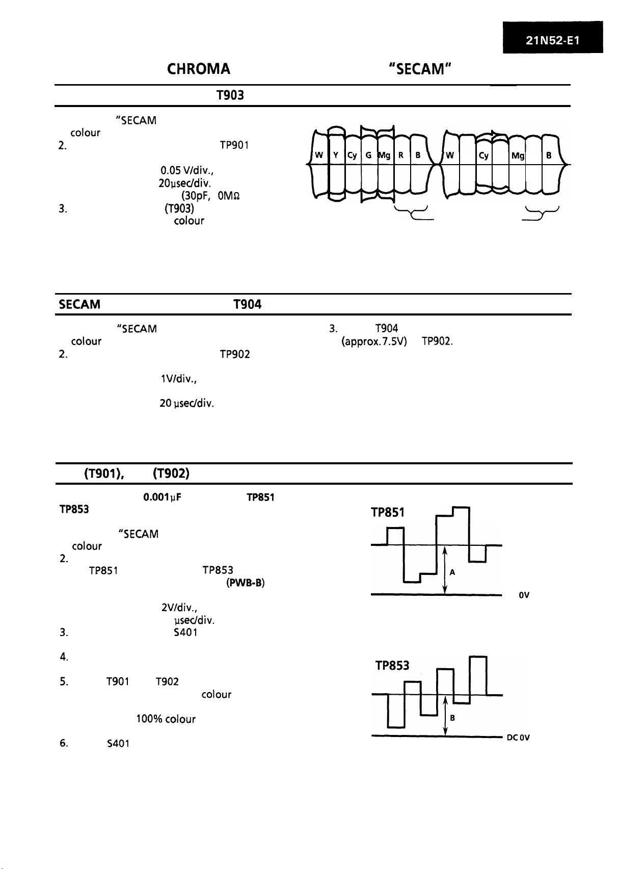
BELL FILTER ADJUSTMENT:
CIRCUIT ADJUSTMENT
I. Receive
COLOUR BAR” signal with
bar generator.
Connect the oscilloscope to TP901 with the
following settings.
l
Voltage Range: 0.05 Wdiv., AC
l
Sweep Time:
l
Probe:
I/I 0
I
or more)
Adjust the Bell Filter (T903) so that the Red and
Blue portions of the
bar signal should
have the same amplitude.
KILLER ADJUSTMENT:
I. Receive
bar generator.
Connect the oscilloscope to
following settings.
l
Voltage Range: IV/div., DC
(Adjust vertical position properly.)
l
Sweep Time:
COLOUR BAR” signal with
with the
Y
G
R
Same amplitude
Adjust T904 to obtain maximum DC voltage
at TP902.
B-Y
Note: Connect a
R-Y
DISCRIMINATOR ADJUSTMENT
capacitor to
and
respectively to filter out interference
noise.
I.
Receive
COLOUR BAR” signal with
generator.
Connect the oscilloscope (with two channels)
to TP851 (R-Y) and the
located on the CRT Socket Unit
(B-Y), both
of the
set.
l
Voltage Range:
l
Sweep Time:
IO
Set service switch
DC
at the Video Cut
position to cut-off the Y-signal.
Set both the Contrast and Brightness controls
to their maximum positions.
Adjust
levels obtained when the
and T902 so that the DC output
control is set
to minimum (black and white level) and those
when set to
saturation become
the same.
Return
to CENTER position.
DC
9
Page 10

SUB-HUE:
I. Receive
2. Connect the oscilloscope to
(B-Y).
3. Turn on the “N” key on the remote controller.
4. Set service switch
at the Video Cut
position to cut-off the Y-signal.
5. Operating the Colour control key on the
remote controller, adjust the B-Y waveform to
6. Adjust Sub-Hue control R835 so that the
waveform is obtained.
7. Return
to CENTER (normal) position.
Same level
Y
G
B-Y
R B
Page 11

ADJUSTMENT OF DEFLECTION LOOP
Note; During the adjustment, keep the unit facing the east.
FOCUS ADJUSTMENT
Receive “MONO SCOPE PATTERN” signal.
Set Contrast and Brightness controls at
CENTER position.
Adjust Focus control to have best focus at the
central area of CRT.
HORIZONTAL CENTERING CONTROL:
This adjustment should be performed
after the purity and convergence
adjustments.
Receive “MONO SCOPE PATTERN” signal.
Adjust
picture is at the position which gives the
relation of A = B .
so that the horizontal center of
Adjust point
VERTICAL LINEARITY CONTROL: R526
Receive “MONO SCOPE PATTERN” signal.
Adjust
picture is at best point.
so that the vertical linearity of
VERTICAL SIZE CONTROL:
Receive “MONO SCOPE PATTERN” signal.
Set the Brightness and Contrast controls at
maximum position.
VERTICAL CENTERING CONTROL:
This adjustment should be performed
after the purity and convergence
adjustments.
Receive “MONO SCOPE PATTERN” signal.
Adjust
picture is at the geometrical center of screen.
so that the vertical center of
Adjust
is at best point.
l Vertical size:
so that the vertical size of picture
(Max. 10%)
Page 12

PURITY ADJUSTMENT
Note: During the adjustment, keep the unit facing the east.
PURITY ADJUSTMENT
Prior to the purity adjustment, warm up the
unit with beam current of more than
a
.
.
Left
,
. . . . . . . .
,
.
. . . .
. . .
. . . . . .
,
,
I
I
,
The beam landing is shifted outwards.
The beam landing is shifted to right.
,
,
, ~~~~~
I
I
I
I
I
I
. . . . . . . . . . . . . . . .
. . . . . . . . . . . . . . . .
. , .
. . . . . . . . . . . .
. . . . . . . . . . . .
. . . . . .
. . . . . . . .
.
.
. . . . . .
. . . . . .
.
. .
Left
. . . . . . . . . . . . . . . . . . . . . . . . . .
. . . . . . . . . . . . . .
.
... . . .,..,.......
. . . . . . . . . . . . . . . . .
. . . . . . . . . . . . . . . . . . . . .
. . . . . . . . . . . . . . .
. . . . . .._ . . . . . . . . . . . . . .
.
.
. . . . . . . . . . . . . .
. . . . .
.
. . . . . .
. . . . . . . . . . . . . . . . . . . . . . . . . . . . . .
. . . . . . . . . . . . . .
. . . . . . . . .
. . . . . . .
. .
. . . . . . . . . . . .
. . . . . . . . . . . . . . . . . . . . . . . .
. . . . . . . . . . . . . . .
.
. . . . . . . . .
. . . . . . . . . . . .
. . . . . . . . . . . . . . . . . .
.
. . . . . . . . . . . . . . . .
. . . . . . . . . . . . . . . . . . . . . . .
Left
,
. . . . . . . . . . . . . . . . . . . . . . . . . . . . . . .
. .
.
. . . . . . . . .
. . . . . .
. . . . . . . . . . . . . .
. . .
. . . . . . . . . .
. . . ..‘...........
. . . . . . .
. . . . . .
.
. . . . . . .
. . . . .
,
. . . . .
,
,
.
.
. . . . . .
,
.
.
. . . . . .
. .
I
I
I
,
,
I
I
Figure A.
Figure
Figure
b
Right
. .
.
. . . . .
. . . . . . . . . . . . . . .
. . . . . .
. . . . . . . . .
.
. . . . . . . . . . . . . . . .
. . .
. . . . . . . . . . . . . . .
. . . . . . . . . . . . . . . . . . . . . . . . . . . . .
...
. . . . . . . . . . . . . . .
I
,
,
. . . . . .
,
. . .
,
. . .
Right
Right
for
Receive the green signal alone and adjust the
beam current to
Fully
coil.
Before the purity adjustment, it is needed to
roughly adjust the static convergence.
Set the purity magnet at the position which
gives zero
than
Adjustment
Observe the green spots (“a” and
microscope as shown Fig. A, and adjust the
purity magnet so that they are at the
specified landing position.
If the right and left green spots are both
deviated outwards from their landing
positions as shown in Fig. B,’ push the
deflection yoke forwards until their positions
are corrected.
If the beam landing is shifted to
as shown in Figs.
degree of the purity magnet so that the beam
landing is correctly positioned.
Adjust the purity magnet so that the beam
landing is correct at either of the central part,
right and left parts of screen, then check that
the green beams at four corners of screen are
all correctly positioned.
Finally, check that the beam landing at any
pat of screen is satisfactory with the Rank “B”
specifications.
IO. If the green beam is positioned to mix with
the other
backward.
l
Outside of the specified landing:
To front of the deflection yoke.
l
inside of the specified landing:
To back of the deflection yoke.
Set the raster rotation at
the unit facing the east).
Tighten the screws of the deflection coil.
Tightening torque:
minutes.
770
the CRT with the
magnetic field.
adjust the opening
pull the deflection yoke
position (with
kg
2 kg.
with a
or left
The beam landing is shifted to left.
Figure
Page 13

CONVERGENCE ADJUSTMENT
Note: During the adjustment, keep the unit facing the east.
CONVERGENCE ADJUSTMENT
This adjustment should be performed
Wedge “a”
/Wedge
magnet
magnet
after the purity magnet adjustment.
Receive “CROSSHATCH PATTERN” signal.
Set. the Brightness control and Contrast control
at MAX position.
STATIC CONVERGENCE
Adjust the opening degree of the 4-pole
magnet and rotate the magnet to converge
red and blue lines.
Adjust the opening degree of the 6-pole
magnet and rotate the magnet to converge
red, blue and green lines.
DYNAMIC CONVERGENCE
Dynamic convergence (convergence of the
three
is accomplished in the following manner.
fields) at the edges of CRT screen
Purity magnet
\
*..._
\
\
\ :
. -cd-
: \
\
Convergence in Fig. a:
insert
between the deflection yoke
and CRT, and tilt the deflection yoke upward
until the
shown in Fig. a is
corrected.
Convergence in Fig.
Insert wedges
and
between the
deflection yoke and CRT, and tilt the
yoke until the
shown in Fig. b is corrected.
Convergence in Fig.
Insert wedge
deeply between the
deflection yoke and CRT, and tilt the
G
B
deflection yoke to right until the
convergence shown in Fig. c is corrected.
Convergence in Fig.
Insert wedge
deflection yoke and CRT, and tilt the
deflection yoke to left until the
convergence shown in Fig. d is corrected.
l
. . . . . . . . . . . . . ...*.....
. . . . . . .
I .
:
. . . . . . . . . . . . . . . .
.
I
I
I
.
I
, G
Figured.
Stick the three wedges onto the CRT, and
apply glass tapes thereon.
Apply lacquer to the deflection yoke screw,
magnet unit (made of purity,
and
pole magnets) and magnet unit screw.
After the adjustment,
receive either the Red or
the Blue signal and check that there is no mixture
with the other
signal.
Page 14

CRT DISPLAY ADJUSTMENT
Note; During the adjustment, keep the unit facing the east.
SIGN POSITION CONTROL: RI 017
Set the channel number at
Display the channel sign by means of the
channel call of remote control on the screen.
Adjust the sign position by
set
mm away from the CRT edge.
so that it is
CRT edge
Page 15

TROUBLE SHOOTING TABLE
NO RASTER
r
Check
and
1
Check F701.
Check T701 pin (1) voltage
290V DC at
AC).
Check + B voltage
PW).
Blown out.
I
Check D702.
Normal
Check CRT connector
bias.
15
Page 16

CIRCUITS TO BE CHECKED:
l
Tuner.
.
l
Automatic Gain Control.
+
Power Source.
NO PICTURE, NO SOUND
Does the noise level
Contrast, Brightness and Sound controls?
at max.
Noise increases but no signal is
received.
I
Check the tuner
+
biases.
+
must be
must be
must be
preset switch at VHF position.
must be
band switch at UHF position.
Check the tuner
I
Normal Abnormal
with the
with the
and
Picture noise decreases but sound
I
level varies greatly.
I
Does the
(11) of connector- ?
I
appear at pin
16
Page 17

CIRCUITS TO BE CHECKED:
l
l
and its adjacent
circuit.
output circuit.
Specific colours are not produced
in colour broadcast reception.
The picture
cyan.
I
is red or
Is some
I
I
produced in
The picture
magenta.
broadcast
is green or
1
Yes
Is the white balance
Readjust the white balance.
The picture
yellow.
properly
is blue or
17
Page 18

CIRCUITS TO BE CHECKED:
l
l
When change channel does
and its adjacent
circuit.
output circuit.
shading.
,
Is some colour produced
in B/W broadcast
Yes
Yes
Check pins
I
Check
bias.
No
Normal
(20) and (21) of
appears but
abnormal
Check pins (22), (23)
and (27) of
I I
I
bias.
18
Check
and its
Page 19

CIRCUITS TO BE CHECKED:
l
and its adjacent
circuit.
output circuit.
NO SPECIFIC COLOUR
Specific colours are not produced
in
VCR NTSC4.43 reception.
19
Page 20

D
I
I
A
I
I
,
iDI
m
I
n
TUNING SWITCH
,
I
I
I
I
SCREEN
1
Page 21

PRINTED WIRING BOARD ASSEMBLIES
Wiring Side
1
I
2
I
3
I
4
I
5
I
6
Page 22

Wiring Side
I
7
I
8
9
I
Page 23

PRINTED WIRING BOARD ASSEMBLIES (Continued)
I
Wiring Side
23
Page 24

Wiring Side
Wiring Side
Wiring Side
I
7
8
9
I
I
Page 25

PRINTED WIRING BOARD ASSEMBLIES (Continued)
Wiring Side
1
I
2
I
3
I
4
I
5
6
1
25
Page 26

DESCRIPTION OF SCHEMATIC DIAGRAM
SAFETY NOTE:
DISCONNECT THE AC PLUG FROM THE AC OUTLET BEFORE
PARTS.
POTENTIAL SHOCK HAZARDS WHEN THE CHASSIS IS
OPERATING.
SURE TO
REPLACE THESE PARTS WITH SPECIFIED
ONES FOR
SERVICE PRECAUTION:
The area enclosed by this line
with AC Mains Voltage.
When servicing the area, connect an isolating transformer
between TV receiver and AC line to eliminate hazard of
electric shock.
is direct/y connected
SOLID STATE DEVICE BASE DIAGRAMS
NOTE:
The unit of resistance “ohm
Meg ohm).
resistors are
capacitors are
The diodes, whose parts code is not described, are the
All resistors are unless otherwise noted.
watt, unless otherwise noted.
unless otherwise noted P
is omitted
= 1000 ohms,
VOLTAGE MEASUREMENT CONDITIONS:
Voltages without parenthesis measured with
or Color Signal.
The voltage in parenthesis represents the value measured
with no signal.
All the voltages were measured by using a high impedance
voltmeter.
B & W
WAVEFORM MEASUREMENT CONDITIONS:
The co/our bar signal applied to the TP40 1 is 1
The tuner AGC voltage is approximately 4V.
TOPVIEW
I
I
I
I
I
I
I
I
L
I-
BASE
COLLECTOR
GATE
1
---
1
-----
COLLECTOR
BASE
EMITTER
BASE
DRAIN
GATE
SOURCE
E
E
I
1
1
9
1
1
--
--
I
I
I
1
I
I
I
I
I
I
Page 27

. . . . . . . . . . . . . . . . . .
. . .
. .
.
. . . .
. . . . ..‘...................................
. .
. .
. .
. . . . . ... . . .. . .
. . . . .
. . . .
. . . .
. . .
. . . .
. . . . . . . . . .
.
. . . . . ... .
. . . . . . . . . . . . ...* . . . . .
.
. . . . . . . . . . . .
. . . . . . . . . . . . . . . . . . . . . . . . . . . . . . . . . . . . . . . . . . . . . . . . .
. . . . . .
. .
. .
. .
. .
. . . .
. . ... . . . . ... ... ... .
. . .. .
.
. . . .
. ... .
. .
. . .... . . . . . . .. .
. ... .
. . . . . . . . ..5....... . . . .
.
. .
. . . .
.
. . . . . . . . . . . . ... >
. .. .
. .
. ..
. . . ... ... .
.. .
.
INFRARED REMOTE CONTROLLER CIRCUIT:
CAUTION: This circuit diagram is original one, therefore there may be a slight difference from yours.
1
I
2
3
I
4
I
6
I
Page 28

WAVE FORMS
1
(H)
(H)
(H)
1
(H)
(H)
(H)
(H)
(H)
(H)
5W3-p
(H)
. .
(H)
(H)
(H)
(H)
(H)
(AC 220V)
28
Page 29

SCHEMATIC DIAGRAM: SUB CIRCUIT
29
Page 30

CAUTION:
I
This circuit diagram is original one, therefore there may be a slight difference from yours.
I
30
Page 31

SCHEMATIC DIAGRAM: MAIN CIRCUIT
Page 32

CAUTION: This circuit diagram is original one, therefore there may be a slight difference from yours.
I
I
I
7
I
8
9
10
I
11
I
12
I
32
Page 33

BLOCK DIAGRAM:
MAIN CIRCUIT
1
2
I
3
33
4
I
5 I
6
Page 34

7
8
9
I
10
11
12
I
34
Page 35

BLOCK DIAGRAM: SUB CIRCUIT
1
2
3
4
I
5
I
6
35
Page 36

7
I
8
9
10
11
12
36
Page 37

PARTS LIST
PARTS REPLACEMENT
Ref. No.
I
Part No.
I
I
Description
Code
I I
MOTHER UNIT
Replacement parts which have these special safety characteristics
identified in this manual: electrical components having such
features are identified by
The use of a substitute replacement part which does not have the
same safety characteristics as the factory recommended
replacement parts shown in this service manual may create
shock, fire or other hazards.
in the Replacement Parts Lists.
“HOW TO ORDER REPLACEMENT PARTS”
To have your order filled promptly and correctly, please furnish
the following informations.
2. REF. NO.
4. DESCRIPTION
I I
Description
Ref. No.
I
1. MODEL NUMBER
3. PART NO.
MARK
I
SPARE PARTS-DELIVERY SECTION
Part No.
PICTURE TUBE
R CRT
R
R DegaussingCoil
J
Purity and Static
Convergence
J
Yoke Positioning
(3
used)
PRINTED WIRING BOARD ASSEMBLIES
(
DUNTK6860WEVO
DUNTK6861
DUNTK6862WEVO
DUNTK6859WEVO
DUNTK6863WEVO
DUNTK6374WEVZ
Mother Unit
Control Unit
CRTSocket Unit
AV/S-Output Unit
Powe Unit
R/C Receiver
S-Converter Unit
IF Unit
LED Unit
Code
I
AK
NOTE:
405,
406,
501,
502,
601,
607,
802,
807,
1001,
1002,
1004,
1006,
1009,
1010,
1011,
1012
301
404,
407,
408,
605,
1003
4403
806,
1005
TUNER
THE PARTS
ASSEMBLY BUT NOT INDEPENDENTLY.
1
J Tuner,UHFNHF
INTEGRATED CIRCUITS
J
J
J
Separator, Vertical
Horizontal
Driver
J
R H
i X 1 1 9 4 C E N 1JMicroprocessor
J
J
TRANSISTORS
J
J 2SCl815(GW)
01
01
E J 2SAlOlS(G)
E J 2SAlOlS(Y)
E J
J
BE
AS
and
AM
AM
AC
AC
AC
AD
37
Page 38

Ref. No.
Part No.
Description
MOTHER UNIT (Continued)
Code
Ref. No.
Part No.
I
DIODES
(Continued)
J
Description Code
I
AA
I
TRANSISTORS
DIODES
(Continued)
J
E J
E J
J
J
J
AA
J
J
J Zener Diode,
J Zener Diode,
J
J
1 OCEZZ J
1 CEZZ J Zener Diode,
J
AA
AD
AA
AA
AD
J
J
J
PACKAGED Cl
J
J Resistor Array
COILS
J 68uH
J
J 100pH
J
Diode,
ITS
AA
AL
AC
A%
Page 39

Ref. No.
Part No.
Description
Code
Ref. No. Part No.
Description
Code
MOTHER UNIT (Continued)
COILS
CERAMIC FILTERS
(Continued)
R
J
J 27pH
J 22pH
J 1uH
J 12pH
J 1pH
J 100pH
J
J
J 5.6/6.OMHzTrap
J Osc.,503kHz
J Osc.,4MHz
AK
AC
CONTROLS
J
J lOk(B) Sub-Brightness,
J lOOk(B)SContrast
J ZOOk(B)VerticalSize
J
J 20k(B) Sub-Colour
CEZZ J
Vertical Linearity,
Sub-Hue
DL-Amp.
CAPACITORS
J 4.7
07M J
J
J
J 1
J 4.7
Tantalum AC
Electrolytic AC
Electrolytic
Electrolytic
Electrolytic AC
Electrolytic AD
Electrolytic
Tantalum AD
Electrolytic
Electrolytic AD
Electrolytic AC
DELAY LINES
J DelayLine
J
TRANSFORMERS
J
1
J
J
R H-DriveTrans.
R FlybackTrans.
J Delay Phase
J
J
R CH-SignOscCoil
AC
AD
AD
AD
AH
AD
AD
AD
Cl
EW477M
J
J
J
J 820~ 2kV Ceramic
500VCeramic AA
Polyester
Polyester
Mylar
Electrolytic AC
Electrolytic
Electrolytic AD
Electrolytic
Electrolytic AD
Electrolytic
AC
AA
AD
AD
Page 40

Ref. No.
Part No.
Description
Code
Ref. No.
Description Code
639
~622
DUNTK6860WEVO
MOTHER UNIT (Continued)
RESISTORS
J 47
J
J
J
R 3.9
J
J 1 k
J
J
J
J
SWITCHES
J Service,
Vertical Center
MISCELLANEOUS PARTS
J
FuseResistor A0
FuseResistor A0
Fuse Resistor A0
Cement
Fuse Resistor
Metal Oxide AA
FuseResistor A0
Metal Oxide A0
Metal Oxide AA
AA
AC
DUNTK6861
CONTROL UNIT
DIODES
QSW-ROOOSPEZZ R S-Wide,
CONTROL
SWITCHES
J Sound Up,
J Stand-by
J lSS119
R lOk(B)
Sound Down,
Channel Down,
P-Control,
P-Control Level Up,
P-Control Level Down,
System,
Power
J
AK
DUNTK6281
CRT SOCKET UNIT
TRANSISTORS
J
COIL
J
CONTROLS
J
J 300(B)
Red Bias,
AC
Green Bias,
Blue Bias
AC
Blue Drive
Page 41

Ref. No.
Part No.
Description
Code
Ref. No. Part No.
Description
Code
DUNTK6281
CRT SOCKET UNIT (Continued)
CAPACITORS
J
J
RESISTORS
J 2.7k
J
MISCELLANEOUS PART
25OVElectrolytic AD
J CRTSocket
AD
AA
AA
AK
DIODES
J
COILS
J 33pH
J 15vH
J 8.2pH
CERAMIC FILTERS
J
J
AA
INTEGRATED CIRCUITS
J Sound
J SoundOutput( AK
P/-l J
TRANSISTORS
01
VSZSC181 SGW-1 J
E J
UNIT
Sound Output(L)
AH
AL
AC
VCEAGAlCW477M J 470
VCEAGAlCW107M J
EW477M J
CAPACITORS ,
Electrolytic AC
Electrolytic AD
J
J
Electrolytic AD
Electrolytic
RESISTORS
J
J
Electrolytic
FuseResistor
FuseResistor
MISCELLANEOUS PART
J 2SC1815(Y)
J
AC
J
AH
Page 42

Ref. No.
Description
Code
Ref. No.
Part No.
Description
Code
704,
746
D708,
D709
714,
D743,
DUNTK6859WEVO
POWER UNIT
INTEGRATED CIRCUITS
TRANSISTORS
1 1 CEZZ J
J
J
E J
J
J
DIODES
J
J
J
J
J
J lSS119
J
J
J RU3AMVl
J
J
J
Diode
J
J
Ax
AA
AC
AD
AC
AC
AA
AK
AA
AK
C702,
703,
704,
705,
707,
715,
716
7
744
729
1
TRANSFORMER
R
CAPACITORS
J 0.22 AC250V
J
AC250V Ceramic AC
J 0.0015
J 330
J 0.033 630VMylar
J
J
J 47
J
J 82p
J
J
J
J 0.012
J 0.0068
J
K J
J
J 470
J
2kV Ceramic
1OOVElectrolytic AC
AH
Polyester
Ceramic AA
AS
Ceramic AC
Electrolytic AC
Ceramic AA
Electrolytic
Mylar
Ceramic
Mylar
Mylar
Ceramic AA
Electrolytic AD
Electrolytic
AA
AA
AA
AA
AD
AA
L702
L704
L705
PACKAGED CIRCUIT
J
COILS
J
J
J
J
J 100pH
J 3.3uH
R
AK
AL
745
C742
J 470
J lOOOp2kV Ceramic AC
J 390 25OVElectrolytic AN
J
Electrolytic AD
Electrolytic
Electrolytic
Page 43

Ref. No.
Part No.
Description
Code
Ref. No. Part No.
Description
Code
R709,
710,
714
R722,
760
R724
R725,
726
R740,
R746
R747,
748
R749,
R750,
751,
752,
753,
R754,
756
DUNTK6859WEVO
POWER UNIT (Continued)
RESISTORS
J
Cement AC
J 2.7
J
J 120k3W
J
J 68k
J 47
5
J 39k
J
J
I J
J 330
J
J
J 47
J
J 390
1 J J 820
J
J 8.2M 1/2WSolid
J 1
J
J 10k
J
J
J 6.8
J J 330
J 22k
J
Cement
Carbon
Carbon
Fuse Resistor
Carbon
Carbon
Carbon
Metal Oxide
Carbon
Carbon
Carbon
Carbon
Carbon
Carbon
Fuse Resistor
Cement AC
FuseResistor
Cement AC
Carbon
Carbon
AA
AC
AA
A6
704
FB702,
MISCELLANEOUS PART
J Fuse,T3.15A
J FuseHolder
J
J
DUNTK6863WEVO
RECEIVER AND LED UNIT
DIODE
J
MISCELLANEOUS PART
J Infrared R/C Receiver AL
S-CONVERTER UNIT
INTEGRATED CIRCUIT
J S-Converter
DIODES
E J lSS119
COILS
J 18pH
J
AD
AC
AN
AA
CERAMIC FILTERS
J
J
J 2.2k
J
Carbon
1/4WCarbon
Carbon
Carbon
J 12MHzOsc.
J
J 10MHzOsc.
J
AD
RFiLCO
J
J
AD
Page 44

Ref. No.
Part No.
IF UNIT
Code
Ref. No.
Part No.
Description
PACKING PARTS
Code
INTEGRATED CIRCUIT
1
J
TRANSISTORS
E J 2SCI906
J
DIODE
J
TRANSFORMERS
J AFT
J P-DetectCoil
J
J
CERAMIC FILTERS
J
1 OCEZZ J
CAPACITORS
J 330
J 1
Electrolytic AC
AD
AK
Electrolytic
AN
AC
AD
PackingCase
CABINET PARTS LOCATION
MISCELLANEOUS PARTS
\
I
R ACCord
R
SUPPLIED ACCESSORIES
ACCESSORIES
R Infrared Remote
Controller
ACCESSORIES
1
Dry Battery,
Size
Service Map.
Terminal
1
CABINET PARTS
1
Not Available
H
H
1
2
3
Cabinet, Front
R Door
R Leg(2 used)
R Window AL
R Speaker Decoration
R Speaker Decoration
R
R Push Latch
R Cabinet, Rear
R
Front
AN
AC
Printed in Japan
 Loading...