

Page 1

21JF2-RU/GA/SA/SF/SS
www.DataSheet4U.com
SERVICE MANUAL
No. S95O521JF2-RU
COLOUR TELEVISION
Chassis No. GA-4M
21JF2-RU
21JF2-GA
21JF2-SA
21JF2-SF
MODELS
In the interests of user-safety (Required by safety regulations in some countries) the set should be restored to its original condition and
only parts identical to those specified should be used.
21JF2-SS
FEATURES
ع
Multi 18 Systems
ع
Full Auto Channel Preset and Auto Channel Skip
ع
100-CH Program Memory
ع
CATV (Hyper Band) Ready
<Used Frequency Synthesizer Tuner>
ع
Black Stretch Circuit
ع
On Timer / Off Timer / Reminder Timer
ع
Blue Back Function
Front AV IN & Rear AV IN / OUT Terminals
ع
Front Headphone Jack
ع
Aperture Control Circuit
ع
Auto Fine Tuning
ع
NTSC Colour Comb Filter (AV THRU)
ع
High Contrast Picture
ع
Hotel Mode
ع
White Temperature Select
ع
ععMulti Languages OSD
(ENG / CHI / FRE / MAL / ARA / RUS)
for Model 21JF2-SF / SS Only.
(ENG / CHI / FRE / MAL / ARA)
for Model 21JF2-GA / SA Only.
(ENG / RUS)
for Model 21JF2-RU Only.
MONO
CONTENTS
CHAPTER 1. SPECIFICATIONS
[1] SPECIFICATIONS ......................................... 1-1
CHAPTER 2. IMPORTANT SERVICE NOTES
[1] IMPORTANT SERVICE NOTES .................... 2-1
CHAPTER 3. ADJUSTMENT PRECAUTIONS
[1] ADJUSTMENT PRECAUTIONS .................... 3-1
[2] ADJUSTMENT ............................................. 3-14
CHAPTER 4. MEMORY MAP
[1] MEMORY MAP .............................................. 4-1
CHAPTER 5. TROUBLE SHOOTING FLOWCHART
[1] TROUBLE SHOOTING FLOWCHART .......... 5-1
CHAPTER 6. SOLID STATE DEVICE BASE DIAGRAM
[1] SOLID STATE DEVICE BASE DIAGRAM........ 6-1
CHAPTER 7. CHASSIS LAYOUT
[1] CHASSIS LAYOUT ........................................ 7-1
[2] BLOCK DIAGRAM: HEADPHONE UNIT........8-1
[3] BLOCK DIAGRAM: MAIN UNIT ....................8-2
CHAPTER 9. DESCRIPTION OF SCHEMATIC DIAGRAM
[1] DESCRIPTION OF SCHEMATIC DIA-
GRAM............................................................9-1
CHAPTER 10. WAVEFORMS
[1] WAVEFORMS .............................................10-1
CHAPTER 11. SCHEMATIC DIAGRAM
[1] SCHEMATIC DIAGRAM: MAIN UNIT..........11-1
[2] SCHEMATIC DIAGRAM: CRT UNIT ........... 11-7
[3] SCHEMATIC DIAGRAM: HEADPHONE
UNIT ............................................................ 11-7
CHAPTER 12. PRINTED WIRING BOARD ASSEMBLIES
[1] PWB-B: CRT UNIT ......................................12-1
[2] PWB-C: HEADPHONE UNIT ......................12-1
[3] PWB-A: MAIN UNIT ....................................12-2
CHAPTER 8. BLOCK DIAGRAM
[1] BLOCK DIAGRAM: CRT UNIT ...................... 8-1
The chassis in this receiver is partially hot. Use an isolation transformer between the line cord plug and power receptacle, when servicing
this chassis. To prevent electric shock, do not remove cover. No user - serviceable parts inside. Refer servicing to qualified service personnel.
Parts Guide
WARNING
SHARP CORPORATION
Page 2

21JF2-RU/GA/SA/SF/SS
www.DataSheet4U.com
21JF2-RU/GA/SA/SF/SS
CHAPTER 1. SPECIFICATIONS
[1] SPECIFICATIONS
Convergence ................................................................................................................ Self Convergence System
...............................................................................................................................
Focus
Sweep Deflection ..................................................................................................................................... Magnetic
Intermediate Frequencies
Picture IF Carrier ................................................................................................................................. 38.9MHz
Sound IF Carrier Frequency
6.5MHz ............................................................................................................................................. 32.4MHz
6.0MHz ............................................................................................................................................. 32.9MHz
5.5MHz ............................................................................................................................................. 33.4MHz
Colour Sub-Carrier Frequency........................................................................................................... 34.47MHz
Power Input ..................................................................................................................... 110 ~ 240V AC 50/60 Hz
Power Consumption
Audio Power Output Rating
Speaker
Size
..............................................................................................................................
Voice Coil Impedance
........................................................................................................................................
............................................................................................................. 2.5W(rms) x 2
.............................................................................................................
Service Manual
UNI-BI Focusing
95W
9 x 5 cm Elliptic (2 pcs)
16 ohms at 400 Hz
Aerial Input Impedance
VHF/UHF .......................................................................................................................... 75 ohms Unbalanced
Receiving System .................................................................................
Receiving Channel
VHF-Channels ......................................................................................... E2(48.25MHz) thru E12(224.25MHz)
UHF-Channels ..................................................................................... E21(471.25MHz) thru E69(855.25MHz)
Dimensions
Cabinet material ..................................................................................................................................... All Plastics
.....................................................................................................................................
PAL I, B/G, D/K & SECAM B/G, D/K, -K1
C1(49.75MHz) thru C12(216.25 MHz)
.
S1(105.25MHz) thru S41(463.25HMz)
C13(471.25MHz) thru C57(863.25MHz)
Width: 605mm
Height: 468mm
Depth: 482mm
Weight(approx): 21.7 kg
Specifications are subject to change without prior notice
1 – 1
Page 3

21JF2-RU/GA/SA/SF/SS
www.DataSheet4U.com
21JF2-RU/GA/SA/SF/SS
CHAPTER 2. IMPORTANT SERVICE NOTES
Service Manual
[1] IMPORTANT SERVICE NOTES
Maintenance and repair of this receiver should be done by qualified service personnel only.
1. SERVICE OF HIGH VOLTAGE SYSTEM AND PICTURE TUBE
When servicing the high voltage system, remove static charge from it by connecting a 10K ohm resistor in series with an insulated wire (such as a test
probe) between picture tube dag and 2nd anode lead. (AC line cord should be disconnected from AC outlet.)
1) Picture tube in this receiver employs integral implosion protection.
2) Replace with the same type number of picture tube for continued safety.
3) Do not lift picture tube by the neck.
4) Handle the picture tube only when wearing shatterproof goggles and after discharging the high voltage completely.
2. X-RAY
This receiver is designed so that any X-Ray radiation is kept to an absolute minimum. Since certain malfunctions or servicing may produce potentially
hazardous radiation with prolonged exposure at close range, the following precautions should be observed:
1) When repairing the circuit, please make sure do not increase the high voltage of the set to more than 30.0kV (at beam 0µA).
2) To keep the set in a normal operation, please make sure it’s function at 26.5kV ± 0.5kV (at beam 1000µA). The set has been factory - adjusted to
the above-mentioned high voltage.
*If there is a possibility that the high voltage fluctuates as a result of the repairs, never forget to check for such high voltage after the work.
3) Do not substitute a picture tube with unauthorizerd types and/or brands which may cause excessive X-ray radiation.
3. BEFORE RETURNING THE RECEIVER
Before returning the receiver to the user, perform the following safety checks.
1) Inspect all lead dress to make certain that leads are not pinched or that hardware is not lodged between the chassis and other metal parts in the
receiver.
2) Inspect all protective devices such as non-metal control knobs, insulating materials, cabinet backs, adjustment and compartment covers or
shields, isolation resistor-capacity networks, mechanical insulators etc.
2 – 1
Page 4

21JF2-RU/GA/SA/SF/SS
www.DataSheet4U.com
21JF2-RU/GA/SA/SF/SS
CHAPTER 3. ADJUSTMENT PRECAUTIONS
Service Manual
[1] ADJUSTMENT PRECAUTIONS
This model's setting are adjusted in two different ways: through the I2C bus control and in the conventional analog manner. The
adjustments via the I2C bus control include preset-only items and variable data.
CAUTION: Make sure TV set in "Normal condition" before switch to Service Mode for adjustment.
Setting the service mode by the microprocessor.
1.
i) Press SERVICE key on the remote controller to set the TV set to SERVICE mode position, and the microprocessor is in input
mode. (Adjustment through the I2C bus control).
ii) Press the MENU key on the remote controller to get ready to select the mode (Adjustment mode, Setting mode, Check mode and Option
mode) one by one.
iii)
Press the CH DOWN / UP key on the remote controller to select the item in Adjustment mode, Setting mode or Option mode.
iv) Using the VOLUME UP/ DOWN key on the remote controller, the data can be modified. Please wait approximately 200 msec for data storage
in EEPROM before select to another mode.
v) In Check mode the data cannot be changed.
vi) Press the SERVICE key again, it will switch to the NORMAL mode position, and the microprocessor is out of the SERVICE mode.
Factory Presetting.
2.
i) Power ON the TV set, press the SERVICE key on the remote controller, then press both the CH UP and VOL UP button on the set
simultaniously for 5secs. Initial values are automatically preset, only when a new EEPROM is used.
ii) The initial data are preset as listed in page 3-7 to 3-13.
iii) Make sure the data need modification or not (Initial data).
Precaution: If haven't done this initialization, it may possibly generate excessive Beam current.
For reference please check with memory map RH-IXB226WJZZ. (See Page 4-1 ~ 4-16)
3.
3 – 1
Page 5
21JF2-RU/GA/SA/SF/SS
www.DataSheet4U.com
1. ADJUSTMENT ITEM
***Below are the adjustment items that should be done, PLS FOLLOW THE PROCEDURE. Otherwise some adjustment items will
not be accurate.
NO *** ADJUSTMENT ITEM EFFECTIVE MODEL REVISION
1BUS SET UP
2 OPTION SET UP
3H-VCO
4VIF-VCO
5 S-TRAP fo
6RF-AGC
7 PURITY ADJ
8 CONVERGENCE ADJ
9 FOCUS ADJ
10 V-SHIFT (50 Hz)
11 H-SHIFT (50 Hz)
12 V-SIZE (50 Hz)
13 SCREEN
14 WHITE BALANCE
15 SUB-BRIGHTNESS
16 SUB-CONTRAST
17 SUB-TINT
18 SUB-COLOR
19 SECAM-OFFSET
20 SIF VCO ADJ
21 BEAM CURRENT CHECK
22 BEAM PROTECTOR CHECK
23 HV PROTECTOR CHECK
24 OTHER PROTECTOR CHECK
25 AV OUT CHECK
26 AV IN CHECK
27 CONTRAST CONTROL CHECK
28 COLOR CONTROL CHECK
29 BRIGHTNESS CONTROL CHECK
30 TINT CONTROL CHECK
31 SHARPNESS CONTROL CHECK
32 CH DISPLAY COLOR CHECK
33 NORMAL DISPLAY CHECK
34 WHITE TEMP CONTROL CHECK
35 COLOR SYSTEM CHECK
36 SOUND SYSTEM CHECK
37 NOISE MUTE CHECK
38 OSD LANGUAGE QUANTITY CHECK
39 HEAD PHONE CHECK
40 SHOCK TEST CHECK
41 ROM CORRECTION CHECK
ALL MODELS
3 – 2
Page 6

21JF2-RU/GA/SA/SF/SS
www.DataSheet4U.com
2. USER DATA IN SERVICE MODE
1) While SERVICE mode ON, EEPROM DATA will switch to the service data. Also, once SERVICE mode OFF, EEPROM will switch back to previous
USER DATA.
2) In the service mode, the user data establish as below,
USER DATA
CONTRAST MAX (60)
COLOUR CENT (0)
BRIGHTNESS CENT (0)
TINT CENT (0)
SHARPNESS CENT (0)
WHITE TEMP STANDARD
S-VOLUME MIN
BLUE BACK OFF
C SYSTEM AUTO
S SYSTEM *1
*1: For each CH, data is same as before switch to Service mode.
The flow of Mode list as following,
* Direct Key-in Mode for Service Items in Service Mode
RC CODE (HEX) R/C KEY NAME SERVICE-ITEM
80 POS 1 R-C UP (IN SERVICE MODE V00)
40 POS 2 G-C UP (IN SERVICE MODE V00)
C0 POS 3 B-C UP (IN SERVICE MODE V00)
20 POS 4 R-C DOWN (IN SERVICE MODE V00)
A0 POS 5 G-C DOWN (IN SERVICE MODE V00)
60 POS 6 B-C DOWN (IN SERVICE MODE V00)
E0 POS 7 R-D UP (IN SERVICE MODE V00)
10 POS 8 B-D UP (IN SERVICE MODE V00)
50 POS 0 B-D DOWN (IN SERVICE MODE V00)
E4 FLASHBACK R-D DOWN (IN SERVICE MODE V00)
E4 FLASHBACK Y-MUTE (BESIDES OF SERVICE MODE V00)
75 WHITE TEMP UP RF-AGC (V01)
F5 WHITE TEMP DOWN VIF-VC0 (V02)
C2 TUNE DOWN H-VCO (V03)
8D SHARPNESS DOWN SUB-CON (V04)
D6 BALANCE LEFT SUB-COL (V05)
0D SHARPNESS UP SUB-BRIGHT (V06)
36 BALANCE RIGHT SUB-TINT (V07)
46 TREBLE UP SUB-SHP (V08)
C6 TREBLE DOWN SUB-COL-YUV (V09)
26 BASS UP SUB-TINT-YUV (V10)
24 COLOUR UP V-SIZE (V11), V-SIZE60 (V17)
54 BRIGHTNESS DOWN V-SHIFT (V12), V-SHIFT60 (V18)
74 TINT DOWN H-SHIFT (V13), H-SHIFT60 (V19)
66 SURROUND UP SCM-BR (V14)
E6 SURROUND DOWN SCM-BB (V15)
C4 CONTRAST DOWN SUB-VOL (V16)
4C PICTURE S-TRAP-BG (V20)
CC HOLD S-TRAP-I (V21)
2C TEXT S-TRAP-DK (V22)
AC CANCEL S-TRAP-M (V23)
EC SIZE S-TRAP-574 (V24)
80 POS 1 R-C UP YUV (IN SERVICE MODE V25)
40 POS 2 G-C UP YUV (IN SERVICE MODE V25)
C0 POS 3 B-C UP YUV (IN SERVICE MODE V25)
20 POS 4 R-C DOWN YUV (IN SERVICE MODE V25)
A0 POS 5 G-C DOWN YUV (IN SERVICE MODE V25)
60 POS 6 B-C DOWN YUV (IN SERVICE MODE V25)
E0 POS 7 R-D UP YUV (IN SERVICE MODE V25)
10 POS 8 B-D UP YUV (IN SERVICE MODE V25)
50 POS 0 B-D DOWN YUV (IN SERVICE MODE V25)
3 – 3
Page 7

RC CODE (HEX) R/C KEY NAME SERVICE-ITEM
www.DataSheet4U.com
E4 FLASHBACK R-D DOWN YUV (IN SERVICE MODE V25)
C1 AUTO ADJ FOR V01, V02, V03, V20, V21, V22, V23, V24
CA T-SET
81 SERVICE MODE
1) Please set the MCL to MCL1 as below:
2) After set the MCL, please set the INITIAL SETTING for each models.
INITIAL 3 : For Singapore and Africa ( All Channel Sound System are set to B/G )
INITIAL 4 : For Middle-East ( All Channel Sound System are set to B/G )
INITIAL 5 : For Russia ( All Channel Sound System are set to D/K )
MCL1 (HEX AE)
CH-No Fv (MHz) Sound Sys
0
1 48.25 B/G
2 62.25 B/G
3 77.25 D/K
4 175.25 B/G
5 182.25 B/G
6 183.25 D/K
7 191.25 D/K
8 196.25 B/G
9 199.25 M
10 210.25 B/G
11 224.25 B/G
12 471.25 B/G
13 487.25 I
14 503.25 B/G
15 575.25 B/G
16 583.25 B/G
17 599.25 B/G
18 621.25 M
19 639.25 D/K
20 703.25 B/G
21 735.25 I
22 767.25 B/G
23 815.25 B/G
24 855.25 I
25 855.25 B/G
26 55.25 M
27 83.25 M
28 183.25 M
29 193.25 M
30 217.25 M
31 471.25 M
32 477.25 M
33 693.25 M
34 885.25 M
35 112.25 B/G
36 168.25 B/G
37
38 294.25 B/G
39 463.25 B/G
40
41 647.25 B/G
42 663.25 B/G
43 679.25 B/G
44 174.95 B/G
45 175.55 B/G
46
47
48
49
21JF2-RU/GA/SA/SF/SS
3 – 4
Page 8
21JF2-RU/GA/SA/SF/SS
www.DataSheet4U.com
MCL1 (HEX AE)
CH-No Fv (MHz) Sound Sys
50
51
52
53
54
55
56
57
58
59
60
61
62
63
64
65
66
67
68
69
70
NOTE: PLL DATA OF ABOVE FREQ SHOULD TAKE THE ACCOUNT OF PIF SETTING IN SERVICE OPTION O04 (VIF) BEFORE STORING INTO
EEPROM.
3 – 5
Page 9

3. SHIPPING SETTING & CHECKING
www.DataSheet4U.com
(1) The following default data has been factory-set for the E2PROM follow by INITIAL DATA selected.
21JF2-RU/GA/SA/SF/SS
ITEMS DATA SETTING
LAST POWER ON
LAST TV/AV MODE TV MODE
LAST POSITION CH 1
FLASHBACK CHANNEL CH 1
1/2 DIGIT ENTRY 2 DIGIT ENTRY
VOLUME 0 (Min)
BLUE BACK OFF
OFF TIMER --:-ON TIMER --:-ON TIMER POSITION -ON TIMER VOLUME -REMINDER --:-AFT ALL CH ON
COLOR SYSTEM ALL CH AUTO
SKIP ALL CH OFF
CONTRAST 60
COLOR 0
BRIGHTNESS 0
TINT 0
SHARPNESS 0
WHITE TEMP 0
(Reference: Geomagnetism Adjustment)
MODEL MAGNETIC FIELD(V, H) nT BACKGROUND LANG. S-SYS LANG QTY
SINGAPORE -10000 40000 12300°K ENGLISH B/G 5
AFRICA -10000 40000 12300°K ENGLISH B/G 5
MID-EAST 30000 20000 18000°KARABICB/G6
RUSSIA 45000 20000 7500°K RUSSIAN D/K 2
INITIAL LANGUAGE SOUND SYSTEM
1 CHINESE D/K
2 CHINESE I
3 ENGLISH B/G
4 ARABIC B/G
5 RUSSIAN D/K
6 MALAY B/G
7 FRENCH D/K
*NOTE FOR OSD TYPE:
2: ENGLISH/RUSSIAN
5: ENGLISH/CHINESE/FRENCH/ARABIC/MALAY
6: ENGLISH/CHINESE/FRENCH/ARABIC/MALAY/RUSSIAN
3 – 6
Page 10

21JF2-RU/GA/SA/SF/SS
www.DataSheet4U.com
**AFTER INITIALIZED THE EEPROM (REFER TO FACTORY PRESETTING), READ DATA FROM EEPROM ADDRESS 00H ~ 03H, AND COM-
PARE TO THE LIST BELOW, IF DIFFERENT, INITIALIZE THE EEPROM.
ADDRESS DATA ADDRESS DATA
00H: 7BH 02H: 72H
01H: 72H 03H: 76H
*** There are four stages of service mode data. First stage data from V00 ~ V31 (Adjustment Mode).
To go into second stage of service mode data, press MENU key. Second stage data from F01 ~ F142 (Setting Mode).
To go into third stage of service mode data, press MENU key. Third stage data is Check Mode.
To go into fourth stage of service mode data, press MENU key. Fourth stage data from O01 ~ O31 (Option Mode).
ADJUSTMENT MODE (FIRST STAGE)
EEPROM ITEMS OSD DATA LENGTH INITIAL DATA FIX/ADJ/AUTO REMARK
R-DRIVE V00 0~127 63 ADJ PLS REFER TO
B-DRIVE V00 0~127 63 ADJ ADJ ITEM FOR
R-CUT V00 0~255 127 ADJ SCREEN AND
G-CUT V00 0~255 127 ADJ WHITE BALANCE
B-CUT V00 0~255 127 ADJ
RF-AGC V01 0~127 50 AUTO
VIF-VCO V02 0~63 31 AUTO
H-VCO V03 0~7 3 AUTO
SUB-CONTRAST V04 0~127 100 ADJ
SUB-COLOR V05 0~127 63 ADJ
SUB-BRIGHT V06 0~255 127 ADJ
SUB-TINT V07 0~127 63 ADJ
SUB-SHARPNESS V08 0~63 43 *FIX BUS SETUP
SUB-COLOR -YUV V09 0~127 90 FIX
SUB-TINT-YUV V10 0~127 63 FIX
V-SIZE 50 Hz V11 0~63 38 ADJ
V-SHIFT 50 Hz V12 0~7 3 ADJ
H-SHIFT 50 Hz V13 0~31 9 ADJ
SECAM-BR V14 0~63 37 ADJ
SECAM-BB V15 0~63 22 ADJ
SUB-VOL V16 0~60 60 FIX
V-SIZE 60 Hz V17 -31~0~+31 0 FIX IF NECESSARY, ADJ
V-SHIFT 60 Hz V18 -7~0~+7 -1 FIX IF NECESSARY, ADJ
H-SHIFT 60 Hz V19 -15~0~+15 +2 FIX IF NECESSARY, ADJ
S-TRAP (BG) V20 0~15 7 AUTO
S-TRAP (I) V21 0~15 7 AUTO
S-TRAP (DK) V22 0~15 7 AUTO
S-TRAP (M) V23 0~15 7 AUTO
S-TRAP (5.74) V24 0~15 7 AUTO
CUTOFF/BKGD YUV V25
R-DRI YUV V25 0~127 63 FIX
B-DRI YUV V25 0~127 63 FIX
R-CUT YUV V25 0~255 127 FIX
G-CUT YUV V25 0~255 127 FIX
B-CUT YUV V25 0~255 127 FIX
SUB-CON YUV V26 0~127 100 FIX
SUB-BRGHT YUV V27 0~255 127 FIX
VS-CORRECT V28 0~63 32 FIX ONLY FOR M61266
VC-CORRECT OFFSET V29 -13~+13 0 FIX ONLY FOR M61266
V LINEARITY V30 0~63 32 FIX ONLY FOR M61266
V LINEARITY OFFSET V31 -13~+13 0 FIX ONLY FOR M61266
3 – 7
Page 11

21JF2-RU/GA/SA/SF/SS
www.DataSheet4U.com
SETTING MODE (SECOND STAGE)
EEPROM ITEMS FUNCTION OSD DATA LENGTH
C.CLIP-LVL CLIP LEVEL CONTRAST CONTROL OF
RGB INPUT
RGB-CLIP CLIPPING OF RGB CONTRAST CON-
TROL
BS BLACK STRETCH F03 0(ON) / 1(OFF) 0 FIX
ABCL ABCL PROCESSING (ACL PROCESSING) F04 0(OFF) / 1(ON) 0 FIX
ABCL-GAIN ABCL PROCESSING GAIN F05 0(LOW) / 1(HIGH) 0 FIX
S-OUT-LVL AUDIO OUTPUT GAIN CONTROL F06 0~127 95 *FIX BUS SETUP
VIF-G P-IF DETECTION GAIN OUTPUT F07 0~7 4 FIX
SHPG SHARPNESS GAIN F08 0(NORMAL) / 1(HIGH) 0 FIX
SHPG-P SHARPNESS GAIN PAL F09 0(NORMAL) / 1(HIGH) 0 FIX
SHPG-S SHARPNESS GAIN SECAM F10 0(NORMAL) / 1(HIGH) 0 FIX
SHPG-N4 SHARPNESS GAIN N443 F11 0(NORMAL) / 1(HIGH) 0 FIX
SHPG-N3 SHARPNESS GAIN N358 F12 0(NORMAL) / 1(HIGH) 1 FIX
YDL Y SIGNAL DELAY F13 0~7 5 FIX
YDL-P Y SIGNAL DELAY PAL F14 0~7 5 FIX
YDL-S Y SIGNAL DELAY SECAM F15 0~7 7 FIX
YDL-N4 Y SIGNAL DELAY N443 F16 0~7 5 FIX
YDL-N3 Y SIGNAL DELAY N358 F17 0~7 5 FIX
YDL-AV Y SIGNAL DELAY AV F18 0~7 6 FIX
YDL-AV-P Y SIGNAL DELAY PAL (AV) F19 0~7 6 FIX
YDL-AV-S Y SIGNAL DELAY SECAM (AV) F20 0~7 7 FIX
YDL-AV-N4 Y SIGNAL DELAY N443 (AV) F21 0~7 6 FIX
YDL-AV-N3 Y SIGNAL DELAY N358 (AV) F22 0~7 6 FIX
YDL-YUV Y SIGNAL DELAY YUV F23 0~7 6 FIX
COL-AV (OFFSET) COLOUR OFFSET AV F24 -31~0~+31 +10 *FIX BUS SETUP
COL-P (OFFSET) COLOUR OFFSET PAL F25 -31~0~+31 0 FIX
COL-S (OFFSET) COLOUR OFFSET SECAM F26 -31~0~+31 +9 FIX
COL-N4 (OFFSET) COLOUR OFFSET N443 F27 -31~0~+31 -8 FIX
COL-N3 (OFFSET) COLOUR OFFSET N358 F28 -31~0~+31 -7 FIX
COL-ADJ (OFFSET) COLOUR OFFSET ADJUST F29 -31~0~+31 0 *FIX BUS SETUP
SHP-AV (OFFSET) SHARPNESS OFFSET AV F30 -31~0~+31 +5 *FIX BUS SETUP
SHP-YUV (OFFSET) SHARPNESS OFFSET YUV F31 -31~0~+31 0 FIX
SHP-P (OFFSET) SHARPNESS OFFSET PAL F32 -31~0~+31 0 FIX
SHP-S (OFFSET) SHARPNESS OFFSET SECAM F33 -31~0~+31 -5 FIX
SHP-N4 (OFFSET) SHARPNESS OFFSET N443 F34 -31~0~+31 0 FIX
SHP-N3 (OFFSET) SHARPNESS OFFSET N358 F35 -31~0~+31 0 FIX
TINT-AV (OFFSET) TINT OFFSET AV F36 -63~0~+63 0 *FIX BUS SETUP
TINT-ADJ (OFFSET) TINT OFFSET ADJUST F37 -63~0~+63 0 *FIX BUS SETUP
TINT-YUV-ADJ (OFF-
SET)
R-R (OFFSET) R-DRIVE OFFSET WHEN WHITE TEMP IS
B-R (OFFSET) B-DRIVE OFFSET WHEN WHITE TEMP IS
R-B (OFFSET) R-DRIVE OFFSET WHEN WHITE TEMP IS
B-B (OFFSET) B-DRIVE OFFSET WHEN WHITE TEMP IS
TRAP CENTER VALUE OF CHROMA TRAP F43 0~3 2 FIX
TRAP-P CENTER VALUE OF CHROMA TRAP PAL F44 0~3 2 FIX
TRAP-S CENTER VALUE OF CHROMA TRAP
TRAP-N4 CENTER VALUE OF CHROMA TRAP N443 F46 0~3 2 FIX
TRAP-N3 CENTER VALUE OF CHROMA TRAP N358 F47 0~3 2 FIX
1W-TV VERT SYNC DETECTION MODE FOR AV
1W-AV VERT SYNC DETECTION MODE FOR TV
V-FREE (NO SYNC) SET VERTICAL TO FORCED FREE RUN
TINT YUV OFFSET ADJUST F38 -63~0~+63 0 FIX
RED
RED
BLUE
BLUE
SECAM
(1 WINDOW/2 WINDOW)
(1 WINDOW/2 WINDOW)
MODE
F01 0(20H) / 1(40H) 0 FIX
F02 0 (CLIP OFF) / 1(CLIP ON) 0 FIX
F39 -63~0~+63 +8 *FIX BUS SETUP
F40 -63~0~+63 -10 *FIX BUS SETUP
F41 -63~0~+63 -3 *FIX BUS SETUP
F42 -63~0~+63 +13 *FIX BUS SETUP
F45 0~3 2 FIX
F48 ACCEPTABLE PERIOD:
0(AUTOMATIC CHANGE)
/ 1(FIX (WIDE))
F49 ACCEPTABLE PERIOD:
0(AUTOMATIC CHANGE)
/ 1(FIX (WIDE))
F50 0(NORMAL) / 1(FRE-
ERUN)
INITIAL
DATA
FIX/ADJ/
AUTO
0FIX
1FIX
0FIX
REMARK
3 – 8
Page 12

21JF2-RU/GA/SA/SF/SS
www.DataSheet4U.com
SETTING MODE (SECOND STAGE)
EEPROM ITEMS FUNCTION OSD DATA LENGTH
AFC2 (NO SYNC) HORIZONTAL AFC2 GAIN F51 0(NORMAL) / 1(DOWN) 0 FIX
GAMMA GAMMA CORRECTION QTY F52 0~3 0 FIX
BS-D/C BLACK STRETCH CONTROL LEVEL F53 0~15 10 FIX
BS-GAIN BLACK STRETCH LEVEL F54 0(NORMAL) / 1(DOWN) 0 FIX
OM-DET OVER MODULATION DETECT F55 0(OFF) / 1(ON) 0 FIX
SL-TV SLICE LEVEL OF SYNC DETECTION TV F56 0~7 2 FIX
SL-AV SLICE LEVEL OF SYNC DETECTION AV F57 0~7 4 FIX
SL-YUV SLICE LEVEL OF SYNC DETECTION YUV F58 0~7 4 FIX
VD2/VD1/AS/FBP-TV VD2 & VD1-VERT SYNC DETECT MIN
WIDTH MSB & LSB RESPECTIVELY, ASTV/AV/YUV SWITCH & CH CHANGE, FBPFLYBACK PULSE SLICE LEVEL (TV)
VD2/VD1/AS/FBP-AV VD2 & VD1-VERT SYNC DETECT MIN
WIDTH MSB & LSB RESPECTIVELY, ASTV/AV/YUV SWITCH & CH CHANGE, FBPFLYBACK PULSE SLICE LEVEL (AV)
VD2/VD1/AS/FBP-YUV VD2 & VD1-VERT SYNC DETECT MIN
WIDTH MSB & LSB RESPECTIVELY, ASTV/AV/YUV SWITCH & CH CHANGE, FBP-
FLYBACK PULSE SLICE LEVEL (YUV)
VDL COLOUR DIFF. INPUT PHASE ADJ F62 0~3 0 FIX
UDL COLOUR DIFF. INPUT PHASE ADJ F63 0~3 0 FIX
AUTO-SCM-KIL-TV SECAM COLOUR KILLER SENSITIVITY
(TV)
SECAM-BGP INTERNAL SECAM BGP TIMING F65 0~3 0 FIX
N45 INHIBIT 50Hz NTSC 4.43 F66 0(NORMAL) / 1(INHIBIT) 0 FIX
TXT-POS-H (TELE-
TEXT)
TXT-POS-V (TELE-
TEXT)
OSD-POS OSD POSITION F69 0~127 9 FIX
CP CHARGE PUMP F70 0(FAST TUNING) /
SMALL-SURR (S-
CTRL)
SUB-BASS (S-CTRL) SUB BASS CONTROL F72 0(0dB), 1(-1dB), 2(-2dB),
SUB-TREB (S-CTRL) SUB TREBLE CONTROL F73 0(0dB), 1(-1dB), 2(-2dB),
AGC-ADJ (S-CTRL) AGC LEVEL ADJUST F74 0(AGC Off), 1(300mVrms),
AGC-SW-OFF
(NICAM)
AGC-GAIN-ADJ
(NICAM)
FM-LEVEL-ADJ
(NICAM)
IGR-LEVEL-ADJ
(NICAM)
NICAM-BG-LVL-ADJ
(NICAM)
NICAM-I-LVL-ADJ
(NICAM)
NICAM-DK-LVL-ADJ
(NICAM)
NICAM-LOW-ERR-LIM
(NICAM)
NICAM-UPP-ERR-LIM
(NICAM)
IGR-GAIN-ADJ (IGR) IGR GAIN ADJUST F84 -6~0~+7 0 FIX
TELETEXT HORIZONTAL POSITION F67 0~63 30 FIX
TELETEXT VERTICAL POSITION F68 0~63 34 FIX
SURROUND MODE SELECT F71 0(EALA EFFECT LARGE)
NICAM AGC SWITCH OFF F75 0(DISABLE, FIX GAIN),
NICAM AGC GAIN ADJUST F76 0~31 16 FIX
FM LEVEL ADJUST F77 -15~0~+15 0 FIX
IGR LEVEL ADJUST F78 -15~0~+15 +1 FIX
NICAM B/G LEVEL ADJUST F79 -15~0~+15 -2 FIX
NICAM I LEVEL ADJUST F80 -15~0~+15 +3 FIX
NICAM D/K LEVEL ADJUST F81 -15~0~+15 -1 FIX
NICAM LOWER ERROR LIMIT F82 0~255 35 FIX
NICAM UPPER ERROR LIMIT F83 0~255 70 FIX
F59 0~15 6 FIX
F60 0~15 14 FIX
F61 0~15 14 FIX
F64 0~3 1 FIX
1(MODERATE SPEED
TUNING)
/ 1(EALA EFFECT SMALL)
3(-3dB), 4(0dB), 5(+1dB),
6(+2dB), 7(+3dB)
3(-3dB), 4(0dB), 5(+1dB),
6(+2dB), 7(+3dB)
2(400mVrms), 3(500Vrms),
4(600mVrms)
1(ENABLE)
INITIAL
DATA
1FIX
0FIX
6FIX
0*FIX
0*FIX
1FIX
FIX/ADJ/
AUTO
REMARK
3 – 9
Page 13
21JF2-RU/GA/SA/SF/SS
www.DataSheet4U.com
SETTING MODE (SECOND STAGE)
EEPROM ITEMS FUNCTION OSD DATA LENGTH
FM-ID-SPEED
(NICAM)
NICAM-AUTO-MUTE NICAM AUTO DETECTION F86 0(MUTE) / 1(DEMUTE) 0 FIX
AUTO-SCM-KIL-AV-
YUV
AFC1-GAIN-TV MSB OF HORIZONTAL AFC GAIN1 (TV) F88 0(NORMAL) / 1(x2) /
AFC1-GAIN-AV MSB OF HORIZONTAL AFC GAIN1 (AV) F89 0(NORMAL) / 1(x2) /
AFC1-GAIN-YUV MSB OF HORIZONTAL AFC GAIN1 (YUV) F90 0(NORMAL) / 1(x2) /
CON-REDUCE CONTRAST (PICTURE LEVEL) CONTROL F91 0(0%)~1(25%)~2(50%) 0 FIX
TAKE-OFF-TV TAKEOFF/BPF OF CHROMA BPF PRO-
TAKE-OFF-AV TAKEOFF/BPF OF CHROMA BPF PRO-
TAKE-OFF-YUV TAKEOFF/BPF OF CHROMA BPF PRO-
C-ANGLE (103 DEG/
95 DEG)
AC-FAIL-WO-BRIGHT PICTURE BLACK LEVEL (BRIGHT) CON-
FORCED-SCM-KIL-TV FORCED SECAM COLOUR KILLER SEN-
FORCED-SCM-KIL-AV-
YUV
R-Y ADJ. COLOUR EDGE IMPROVEMENT F99 0(DISABLE) / 1(ENABLE) 1 FIX
V-DEMUTE-DELAY VIDEO DEMUTE DELAY F100 0~255 0 *FIX BUS SETUP
S-DEMUTE-DELAY SOUND DEMUTE DELAY F101 0~255 0 *FIX BUS SETUP
MER S-BOOSTER FREQ. CHARACTERISTIC
MEL1 S-BOOSTER LEVEL1 F103 0~255 150 FIX
MEL2 S-BOOSTER LEVEL2 F104 0~255 156 FIX
MEL3 S-BOOSTER LEVEL3 F105 0~255 163 FIX
MEL4 S-BOOSTER LEVEL4 F106 0~255 165 FIX
MEL5 S-BOOSTER LEVEL5 F107 0~255 170 FIX
MEL6 S-BOOSTER LEVEL6 F108 0~255 180 FIX
S-ST-POINT S-BOOSTER START POINT F109 0~60 21 FIX
S-SP-POINT S-BOOSTER STOP POINT F110 0~60 60 FIX
S-STEP S-BOOSTER STEP F111 0~60 7 FIX
POW-STORAGE CONTRAST/BRIGHTNESS INCREASE
S-B-BASS S-BOOSTER BASS LIMITER (WHEN S-
S-B-TREB S-BOOSTER TREBLE LIMITER (WHEN S-
S-BASS S-BOOSTER BASS LIMITER (WHEN S-
S-TREB S-BOOSTER TREBLE LIMITER (WHEN S-
V-STD-TV VERTICAL STANDARD SIGNAL DETEC-
V-STD-AV VERTICAL STANDARD SIGNAL DETEC-
V-STD-YUV VERTICAL STANDARD SIGNAL DETEC-
WO-Bright-after-WO-
TIME
WO-Contrast-after-
WO-TIME
WO-Bright-before-WO-
TIME
WO-Contrast-before-
WO-TIME
WO-TIME WHITE OUT F124 0~31 0 FIX
FM SOUND IDENTIFICATION MODE F85 0(SLOW) / 1(MEDIUM) /
SECAM COLOUR KILLER SENSITIVITY
(AV/YUV)
CESSING TV
CESSING AV
CESSING YUV
CHROMA MODULATION ANGLE F95 0(103DEG) / 1(95DEG) 1 FIX
TROL - AC FAILURE
SITIVITY (TV)
FORCED SECAM COLOUR KILLER SEN-
SITIVITY (AV/YUV)
CONTROL
GRADUALLY
BOOSTER ON)
BOOSTER ON)
BOOSTER OFF)
BOOSTER OFF)
TOR SWITCH (TV)
TOR SWITCH (AV)
TOR SWITCH (YUV)
WHITE OUT BRIGHT AFTER WHITE OUT
TIME
WHITE OUT CONTRAST AFTER WHITE
OUT TIME
WHITE OUT BRIGHT BEFORE WHITE
OUT TIME
WHITE OUT CONTRAST BEFORE WHITE
OUT TIME
F87 0~3 1 FIX
F92 0(BPF) / 1(TAKEOFF) 1 FIX
F93 0(BPF) / 1(TAKEOFF) 0 FIX
F94 0(BPF) / 1(TAKEOFF) 0 FIX
F96 0~255 255 FIX
F97 0~3 2 FIX
F98 0~3 2 FIX
F102 0~255 70 FIX
F112 0(DISABLE) / 1(ENABLE) 1 FIX
F113 -30~0~+30 +15 FIX
F114 -30~0~+30 +15 FIX
F115 -30~0~+30 +30 FIX
F116 -30~0~+30 +30 FIX
F117 0(DISABLE) / 1(ENABLE) 0 FIX
F118 0(DISABLE) / 1(ENABLE) 0 FIX
F119 0(DISABLE) / 1(ENABLE) 0 FIX
F120 0~255 255 FIX
F121 0~127 127 FIX
F122 0~255 255 FIX
F123 0~127 127 FIX
2(FAST) / 3(OFF)
2(x1.5) / 3(3.5)
2(x1.5) / 3(3.5)
2(x1.5) / 3(3.5)
INITIAL
DATA
FIX/ADJ/
AUTO
1FIX
0FIX
3FIX
3FIX
REMARK
3 – 10
Page 14

21JF2-RU/GA/SA/SF/SS
www.DataSheet4U.com
SETTING MODE (SECOND STAGE)
EEPROM ITEMS FUNCTION OSD DATA LENGTH
A2-ID-Response SETTING IDENTIFICATION RESPONSE
R-DRI YUV OFFSET RGB OUTPUT RED GAIN OFFSET (YUV) F126 -63~0~+63 0 FIX
B-DRI YUV OFFSET RGB OUTPUT BLUE GAIN OFFSET (YUV) F127 -63~0~+63 0 FIX
R-CUT YUV OFFSET RGB OUTPUT-RED BIAS LEVEL OFFSET
G-CUT YUV OFFSET RGB OUTPUT-GREEN BIAS LEVEL OFF-
B-CUT YUV OFFSET RGB OUTPUT-BLUE BIAS LEVEL OFFSET
CON YUV OFFSET SUB-CONTRAS OFFSET (YUV) F131 -63~0~+63 0 FIX
BRT YUV OFFSET SUB-BRIGHT OFFSET (YUV) F132 -63~0~+63 0 FIX
SHP ANT-ONII OFF-
SET
WAIT MD TIME SETTING CYCLE PROCESS TIME AT
Contrast OFFSET CONTRAST (PICTURE LEVEL) OFFSET F135 -63~0~+63 0 FIX
Bright OFFSET PICTURE BLACK LEVEL (BRIGHT) OFF-
CR-PEDESTEL-ADJ Cr SIGNAL LEVEL ADJUSTMENT F137 0~15 8 FIX ONLY FOR
CB-PEDESTEL-ADJ Cb SIGNAL LEVEL ADJUSTMENT F138 0~15 8 FIX ONLY FOR
SIF-PAL SOUND S/N SWITCH FOR PAL F139 0(DISABLE) / 1(ENABLE) 0 FIX ONLY FOR
AV2 BRIGHTNESS
OFFSET
BASS OFFSET BASS OFFSET F141 -30~0~+30 0 FIX
TREBLE OFFSET TREBLE OFFSET F142 -30~0~+30 0 FIX
TIME
(YUV)
SET (YUV)
(YUV)
SHARP ANT-ON II OFFSET FOR VIDEO
TONE
LOW POWER
SET
AV2 BRIGHT OFFSET F140 -15~0~+15 +7 FIX
F125 0(NORMAL) / 1(FAST) 1 FIX
F128 -63~0~+63 0 FIX
F129 -63~0~+63 0 FIX
F130 -63~0~+63 0 FIX
F133 -31~0~+31 0 FIX
F134 0~4 2 FIX
F136 -63~0~+63 0 FIX
INITIAL
DATA
FIX/ADJ/
AUTO
REMARK
M62166
M62166
M62166
3 – 11
Page 15

21JF2-RU/GA/SA/SF/SS
www.DataSheet4U.com
OPTION MODE (FOURTH STAGE)
EEPROM ITEMS OSD DATA LENGTH INITIAL DATA REMARK
***HOTEL MODE O01 0 (0FF) / 1 (0N) 0 OPTION SET UP
***HTL-POS O02 0~99,-- -- OPTION SET UP
***HTL-VOL O03 0~60,-- -- OPTION SET UP
VIF O04 0 (38.0) / 1 (38.9) 1 OPTION SET UP
SECAM O05 0 (DISABLE) / 1 (ENABLE) 1 OPTION SET UP
N443(RF) O06 0 (DISABLE) / 1 (ENABLE) 1 OPTION SET UP
N358(RF) O07 0 (DISABLE) / 1 (ENABLE) 1 OPTION SET UP
FORCE-COL O08 0 (DISABLE) / 1 (ENABLE) 0 OPTION SET UP
S-SYS O09 1(BG ONLY)~15(ALL) 15 OPTION SET UP
AV O10 0 (DISABLE) / 1 (ENABLE) 1 OPTION SET UP
AV2 O11 0 (DISABLE) / 1 (ENABLE) 1 OPTION SET UP
YUV O12 0 (DISABLE) / 1 (ENABLE) 1 OPTION SET UP
S-CTRL O13 0 (DISABLE) / 1 (ENABLE) 1 OPTION SET UP
NICAM O14 0 (DISABLE) / 1 (ENABLE) 0 OPTION SET UP
A2 O15 0 (DISABLE) / 1 (ENABLE) 0 OPTION SET UP
TELETEXT O16 0 (DISABLE) / 1 (ENABLE) 0 OPTION SET UP
BILLINGUAL O17 0 (DISABLE) / 1 (ENABLE) 0 OPTION SET UP
LANGUAGE O18 1~255 63 OPTION SET UP
SEARCH-SPEED O19 1(350)~2(450)~3(550)~4(650)~5(750) 3 OPTION SET UP
R/C-MENU O20 0 (ENABLE) / 1 (DISABLE) 0 OPTION SET UP
LED-CONT O21 0 (ONE LED) / 1 (TWO LED) 0 OPTION SET UP
S-BOOSTER O22 0 (DISABLE) / 1 (ENABLE) 0 OPTION SET UP
SHARP-LOGO O23 0 (DISABLE) / 1 (ENABLE) 0 OPTION SET UP
YUV BKGD ADJ O24 0 (DISABLE) / 1 (ENABLE) 0 OPTION SET UP
WHITE BACK O25 0 (DISABLE) / 1 (ENABLE) 1 OPTION SET UP
BOOSTER O26 0 (DISABLE) / 1 (ENABLE) 0 OPTION SET UP
****MESSAGE O27 0 (DISABLE) / 1 (ENABLE) 0 OPTION SET UP
****MESSAGE SCROLL TIME O28 Message Display Timing 0 OPTION SET UP
LNA TUNER O29 0(Alps) / 1(Matsushita) 0 OPTION SET UP
ONE CHIP IC O30 0(M61260 & M61262) / 1(M61266) 0 OPTION SET UP
MESSAGE INPUT TIMMING O31 0~4 2 OPTION SET UP
*** HOTEL MODE
OPERATION OF HOTEL MODE:
WHEN CHANGE SERVICE DATA O01 TO 1, HOTEL MODE IS ON
WHEN HOTEL MODE IS ON,
1. Max volume data is determined by option setting HTL-VOL (O03)
2. Channel position after POWER ON is determined by option setting HOTEL-POS (O02) (if option setting HOTEL-POS
is not set, processing is according to last position data).
3. User data updates of EEPROM regarding the video and audio control is not allowed.
4. Preset mode is disable.
5. CH SETTING menu is not available.
3 – 12
Page 16

21JF2-RU/GA/SA/SF/SS
www.DataSheet4U.com
4. ADJ ITEM: BUS SET UP (1 ST & 2ND STAGE SERVICE DATA)
SERVICE ITEMS 21JF2-RU 21JF2-GA/SA 21JF2-SF 21JF2-SS
V08 SUB-SHARPNESS 46 46 46 46
F06 S-OUT-LVL 105 105 105 105
F24 COL-AV +10 0 0 0
F29COL-ADJ 0 +5+5+5
F30SHP-AV +1+1+1+1
F36TINT-AV 0 -3-3-3
F37 TINT-ADJ 0 -8 -8 -8
F39 R-R +8 0 0 0
F40B-R -10-9-9-9
F41 R-B -3 -6 -6 -6
F42 B-B (OFFSET) +16 +8 +8 +8
5. ADJ ITEM: OPTION SET UP (4TH STAGE SERVICE DATA)
SERVICE ITEMS 21JF2-RU 21JF2-GA/SA 21JF2-SF 21JF2-SS
O01 HTL MODE 0 (0FF) / 1 (0N) 0 0 0 0
O02 HTL-POS 0~99,-- -- -- -- -O03 HTL-VOL 0~60,-- -- -- -- -O04 VIF 0 (38.0) / 1 (38.9) 1 1 1 1
O05 SECAM 0 (DISABLE) / 1 (ENABLE) 1 1 1 1
O06 N443(RF) 0 (DISABLE) / 1 (ENABLE) 1 1 1 1
O07 N358(RF) 0 (DISABLE) / 1 (ENABLE) 0 0 0 0
O08 FORCE-COL 0 (DISABLE) / 1 (ENABLE) 0 0 0 0
O09 S-SYS 1(BG ONLY)~15(ALL) 7 7 7 7
O10 AV 0 (DISABLE) / 1 (ENABLE) 1 1 1 1
O11 AV2 0 (DISABLE) / 1 (ENABLE) 1 1 1 1
O12 YUV 0 (DISABLE) / 1 (ENABLE) 0 0 0 0
O13 S-CTRL 0 (DISABLE) / 1 (ENABLE) 0 0 0 0
O14 NICAM 0 (DISABLE) / 1 (ENABLE) 0 0 0 0
O15 A2 0 (DISABLE) / 1 (ENABLE) 0 0 0 0
O16 TEXT 0 (DISABLE) / 1 (ENABLE) 0 0 0 0
O17 BIL 0 (DISABLE) / 1 (ENABLE) 0 0 0 0
O18 LANG 1~255 9 55 63 63
O19 SEARCH-SP 1(350)~2(450)~3(550)~4(650)~5(750) 3 3 3 3
O20 R/C MENU 0 (ENABLE) / 1 (DISABLE) 1 1 1 1
O21 LED-CONT 0 (ONE LED) / 1 (TWO LED) 0 0 0 0
O22 S-BOOSTER 0 (DISABLE) / 1 (ENABLE) 0 0 0 0
O23 SHARP-LOGO 0 (DISABLE) / 1 (ENABLE) 0 0 0 0
O24 YUV BKGD ADJ 0 (DISABLE) / 1 (ENABLE) 0 0 0 0
O25 WHITE BACK 0 (DISABLE) / 1 (ENABLE) 0 0 0 0
O26 BOOSTER 0 (DISABLE) / 1 (ENABLE) 0 0 0 0
O27 MESSAGE 0 (DISABLE) / 1 (ENABLE) 0 0 0 0
O28 MESSAGE SCROLL TIME 0 ~ 20 0 0 0 0
O29 LNA TUNER 0(Alps) / 1(Matsushita) 0 0 0 0
O30 ONE CHIP IC 0(M61260 & M61262) / 1(M61266) 0 0 0 0
O31 MSG IN TM 2 2 2 2
3 – 13
Page 17
21JF2-RU/GA/SA/SF/SS
www.DataSheet4U.com
[2] ADJUSTMENT
ADJUSTMENT PRECAUTION: Makesure TV Set is in “Normal Condition” before switch to Service Mode for Adjustment.
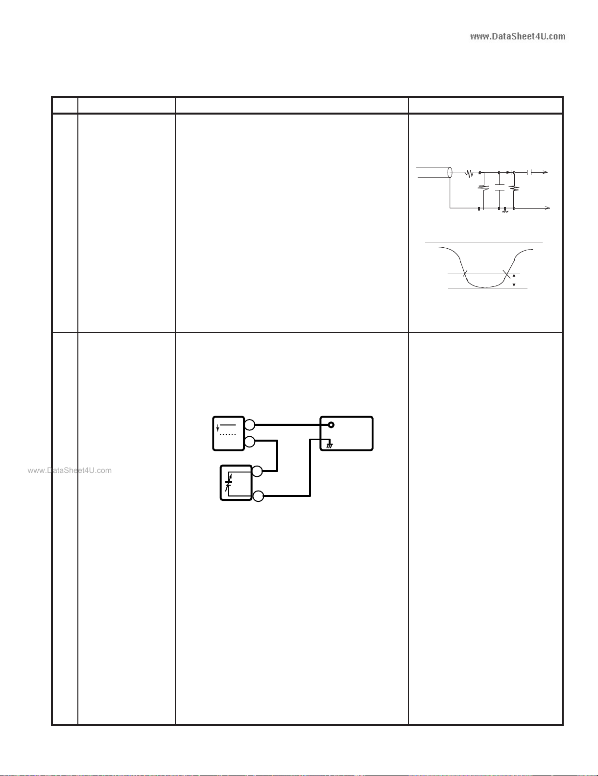
1. PIF ADJUSTMENT
No.
Adjustment point
Tuner IFT
1 1. Get the tuner ready to receive the CH. E - 9
( PRESET )
Adjustment procedure/conditions Waveform and others
signal,but with no signal input.
Adjust the PLL data.
2. Connect the sweep generator's output cable to
the tuner antenna. ( RF SWEEP )
3. Adjust the sweep generator's to 80dBµV.
4. Connect the response lead ( use LOW IMPEDANCE probe with wave detector ; see Fig.1 ) to
the tuner's IF output terminal. ( This terminal must
have the probe alone connected ).
5. Set the RF AGC to 0 - 6 V with no saturation with
the waveform.
6. Adjust the tuner IF coil to obtain the waveform as
showninFig.2.
Note: Be sure to keep the tuner cover in posi-
tion during this adjustment.
2
RF-AGC
TAKE OVER
1. Receive "PAL COLOUR BAR" signal.
Signal Strength: 56 ± 1dBµV (75 ohm open)
POINT ADJUSTMENT
2
(I
C BUS
CONTROL)
(AUTO &
MANUAL ADJ)
2. Connect the oscilloscope to TP201 (Tuner’s AGC
Terminal) as shown in Fig. 3-1.
Oscilloscope
0.1V
TP201+
—
Bias box
TV Set
+
—
»»Bias box: About 4.5 V
1000p
10k
Oscilloscope
100k
1n60
1000p
IF OUT
75ohm
Fig.1
E-9 CH
PC
-1.5+/-0.8dB
Fig.2
* for Auto ADJ
1)Receive “PAL COLOUR BAR”
signal.
signal strength: 56
± 1dBµV(75
ohm open)
1)Go to service mode.
2)Go to service data V01, press
R/C to operate auto key ( Hex
C1) and confirm the ‘OK’
display on the screen.
3)If appear NG, increase data
some step and pls repeat step
4)Proceed step 4 & 5 in manual
mode.
2.
Fig. 3-1
3. Call "V01" mode in service mode. Adjust the "V01"
bus data to obtain the Tuner output pin drop
0.1~1.0V below maximum voltage.
4. Change the antenna input signal to 63~67dBµV,
and make sure there is no noise.
5. Turn up the input signal to 90~95 dBµVtobesure
that there is no cross modulation beat.
3 – 14
Page 18

21JF2-RU/GA/SA/SF/SS
www.DataSheet4U.com
2. PURITY ADJUSTMENT
No.
Adjustment point
PURITY ADJ.1
Adjustment procedure/conditions Waveform and others
1. Receive the GREEN-ONLY signal. Adjust the
beam current to ~700 µA.
2. Degauss the CRT enough with the degausing coil.
Note: Follow the Job Instruction Sheet to adjust
the magnetic field.
(Reference: page 3-6)
3. Maintain the purity magnet at the zero magnetic
field and keep the static convergence roughly
adjusted.
4. Observe the points a, b, as shown in Fig. 1-1
through the microscope. Adjust the landings to A
rank requirement.
5. Orient the raster rotation to 0 eastward.
6. Tighten up the deflection coil screws.
Tightening torque: 108 ± 20N(11± 2kgf)
7. Make sure the CRT corners landing meet the A
rank requirements. If not, stick the magnet sheet
to correct it.
Note: This adjustment must be done after
warming up the unit for 30 minutes or
longer with a beam current over 700
Note:
Set to service mode by remote con-
µ
A.
troller then press factory process R/C
RGB key to change to RGB mono colour mode.
* For the following colours press R/C RGB(Hex 7E)
key to change.
a
30mm 30mm
Fig. 1-1
b
A
B
A=B
Fig. 1-2
Rank "A"
(on the right of the CRT)
GREEN
ONLY
BLUE
ONLY
Signal-colour
screen cleared
A
RED
ONLY
B
A=B
Fig. 1-3
Rank "A"
(on the left of the CRT)
* Press R/C RGB key for 1 sec-
ond in NORMAL MODE, the
colour will change to RGB
mono colour mode.
3 – 15
Page 19

3. CONVERGENCE ADJUSTMENT
www.DataSheet4U.com
21JF2-RU/GA/SA/SF/SS
No.
1
Adjustment point
CONVERGENCE
ADJ.
(Tobedone
after the purity
adjustment.)
Adjustment procedure/conditions Waveform and others
1. Receive the "Crosshatch Pattern" signal.
2. Using the remote controller, call NORMAL mode.
Static convergence
1. Turn the 4-pole magnet to a proper opening angle in order to superpose the blue and red colours.
2. Turn the 6-pole magnet to a proper opening angle in order to superpose the green colour over
the blue and red colours.
Dynamic convergence
1. Adjust the convergence on the fringes of the
screen in the following steps.
a) Fig. a: Drive the wedge at point "a" and swing
the deflection coil upward.
b) Fig. b: Drive the wedge at point "b" and "c" and
swing the deflection coil downward.
c) Fig. c: Drive the "c" wedge deeper and swing
the deflection coil rightward.
d) Fig. d: Drive the "b" wedge deeper and swing
the deflection coil leftward.
2. Fix all the wedges on the CRT and apply glass
tape over them.
3. Apply lacquer to the deflection yoke lock screw,
magnet unit (purity, 4-pole, 6-pole magnets) and
magnet unit lock screw.
BGR
B
G
R
Fig. a
RGB
R
G
B
Fig. b
B
RGB
G
R
Fig. c
R
BGR
G
B
Finally received the Red-only and Blue-only signals to make sure there is no other colours on the
screen.
4-pole magnet
6-pole magnet
CRT neck
Lacquer
Purity magnet
20mm
About
100Deg
Lacquer
Wedge
"b"
Fig. d
Wedge "a"
About
100Deg
Wedge
"c"
3 – 16
Page 20

21JF2-RU/GA/SA/SF/SS
www.DataSheet4U.com
4. H-VCO, VIF-VCO & S-TRAP fo ADJUSTMENT
No.
1
2
Adjustment point
H-VCO ADJ
2
(I
C BUS
CONTROL)
(AUTO &
MANUAL ADJ)
VIF-VCO ADJ
2
(I
C BUS
CONTROL)
(AUTO &
MANUAL ADJ)
Adjustment procedure/conditions Waveform and others
(MANUAL ADJ)
1) In No signal (RASTER) condition.
2) Go to service mode, choose service data V03.
3) Connect oscilloscope to IC801 pin11, adj V03 until
freq become 15.625±0.15 KHz
(Auto Adj)
1) In No signal (RASTER) condition.
2) Go to service mode.
3) Choose service data V03, by pressing R/C Auto
(Hex C1) key, OSD will appear “OK” at screen.
4) If appear “NG” pls repeat step 3.
(Manual ADJ)
1) In No signal (RASTER) condition.
2) Go to service mode, choose service data V02.
3) Connect oscilloscope to IC801 pin2, adj V02 until
voltage become 2.5±1V.
(Auto Adj)
1) In No signal (RASTER) condition.
2) Go to service mode, choose service data V02.
3) Press the R/C Auto (Hex C1) key, OSD will appear
“OK” at screen.
4) If appear “NG” pls repeat step 3.
This adjustment must be done
after aging at least 3 minutes.
S-TRAP fo
3
ADJ
2
(I
CONTROL)
(AUTO &
MANUAL ADJ)
C BUS
(Manual ADJ)
1) In No signal (RASTER) condition.
2) Go to service mode, choose service data V21.
3) Connect oscilloscope to TP 801, adj V21 until
voltage become Min (below 5 V).
4) After that pls adj service data V20 & V24 same as
“V21”, V22 to “V21-1”, V23 to “V21+2”.
(Auto Adj)
1) In No signal (RASTER) condition.
2) Go to service mode, choose service data V21.
3) Press the R/C Auto (Hex C1) key, OSD will appear
“OK” at screen.
4) If appear “NG” pls repeat step 3.
3 – 17
Page 21

5. SCREEN, WHITE BALANCE, SUB-BRIGHTNESS & SUB-CONTRAST ADJUSTMENT
www.DataSheet4U.com
No.
Adjustment point
1
SCREEN
ADJUSTMENT
2
(I
C BUS
CONTROL)
Adjustment procedure/conditions Waveform and others
1) In window pattern signal condition.
R-CUTOFF (R-C) UP
R-CUTOFF (R-C) DOWN
2) Go to service mode, then select V00.
G-CUTOFF (G-C) UP
G-CUTOFF (G-C) DOWN
3)
By pressing R/C key S-Mute (Hex E8), R-D
auto switch to 63, B-D auto switch to 63, R-
C auto switch to 127, G-C auto switch to
127, B-C auto switch to 127, Subbrightness V06 auto switch to 127.
Y-mute & Vertical off, screen will be in
B-CUTOFF (B-C) UP
B-CUTOFF (B-C) DOWN
R-DRIVE (R-D) UP
R-DRIVE (R-D) DOWN
B-DRIVE (B-D) UP
B-DRIVE (B-D) DOWN
vertical cut-off condition.
4)
Adjust the Screen so that cut-off line appear in low bright, then judge that whether
the cut-off line appear in Red or Green or
Blue color, in this condition between R-C &
G-C & B-C, fix the data of the color appear
in cut-off line and adj the other two cut-off
data (Note 1) so that cut-off line color become white.
21JF2-RU/GA/SA/SF/SS
RC key "1" (HEX 80)
RC key "4" (HEX 20)
RC key "2" (HEX 40)
RC key "5" (HEX A0)
RC key "3" (HEX C0)
RC key "6" (HEX 60)
RC key "7" (HEX E0)
RC key "Flashback" (HEX E4)
RC key "8" (HEX 10)
RC key "0" (HEX 50)
WHITE
2
BALANCE ADJ
(to be done
after screen
adj)
2
C BUS
(I
CONTROL)
5)
Turn the screen VR of FBT so that cut-off
line just disappear and use R/C by pressing key S-Mute (Hex E8) to disable the Ymute & V-cut so that picture appear in normal mode.
WHITE (HIGH BEAM) ( In Window Pattern
1)
Signal)
First use Minolta Color Analyzer CA100, let
the gun point at Dark White position (as
drawing attach), Adj V06 until LUMI-
NANCE Y become 5 cd/m2, then let the
gun point at White position ( as drawing attach), Adj V04 until LUMINANCE Y become: 160 cd/m2.
Adj the R-D & B-D until the axis of color
temperature become
o
K X : 300
7500
Y : 310
12300oK X : 272
Y : 275
o
18000
K X : 255
Y : 255
DARK WHITE (LOW BEAM) (In Window
2)
Pattern Signal)
Let the gun point at Dark White position, if
the color temperature data shift away from
the data adjusted in step 1, adjust R-C, G-
C & B-C but between them, first color
appears in Screen adj item 1)-4 is fixed,
adj the other two so that to obtain the similar axis as above.
** Repeatstep1&2togetaregulatedposition
5.5% IRE
*Note :
WINDOW PATTERN SIGNAL
White
50% IRE
Signal using W/B Pattern Generator
SX-1006 (IWATSU) or equivalent.
Window Pattern Signal output level
are as above:
Dark White
9.5% IRE
3 – 18
Page 22

21JF2-RU/GA/SA/SF/SS
www.DataSheet4U.com
No.
Adjustment point
Adjustment procedure/conditions Waveform and others
SUB-
3
BRIGHTNESS
(to be done
after screen,
white balance
adj)
(I
CONTROL)
4
SUBCONTRAST
(to be done
after screen,
white balance
adj,
sub-brightness adj)
(I
CONTROL)
2
C BUS
2
C BUS
1) In Window Pattern Signal condition.
2)
Using Minolta Color Analyzer CA-100, let the
gun point at Dark White position (as attach
drawing), adjust V06 Bus data until LUMI-
NANCEY=3
± 0.5 cd/m2.
1) In Window Pattern Signal condition.
2)
Using Minolta Color Analyzer CA-100, let the
gun point at White position (as attach drawing),
adjust V04 Bus data until LUMINANCE Y = 160
± 10cd/m2
WINDOW PATTERN SIGNAL
Dark White
WINDOW PATTERN SIGNAL
White
Beam Current
5
Check
1) Receive the “Monoscope Pattern” signal.
2) Press R/C to set Picture NORMAL condition.
3) Connect the DC miliammeter between TP 603
(+)&TP602(-).
(Full Scale: 3mA Range)
4) Beam current must be within 1000±100
µA .
3 – 19
Page 23

6. HORIZONTAL, VERTICAL, DEFLECTION LOOP and FOCUS ADJUSTMENT
www.DataSheet4U.com
21JF2-RU/GA/SA/SF/SS
No.
1
2
3
Adjustment point
H-SHIFT
2
CBUS
(I
CONTROL)
(to be done
after purity
adj)
V-SHIFT
2
CBUS
(I
CONTROL)
(to be done
after purity
adj)
V-SIZE
2
CBUS
(I
CONTROL)
(to be done
after purity,
V-shift adj)
Adjustment procedure/conditions Waveform and others
1) Receive Monoscope Pattern Signal (PAL 50 Hz)
2) Choose the service data V13.
3) Adjust the V13 bus data to have a balance position
to spec of A=B (as attach drawing)
4) If cannot make it to A=B, adjust from the best point
so that B slightly smaller than A.
1) Receive Monoscope Pattern Signal (PAL 50 Hz)
2) Choose the service data V12.
3) Adjust V12 bus data to have a most acceptable
vertical position, the monoscope pattern should
be Balance in vertical position.
Note: B line (Monoscope middle line) must
same or nearest higher position to the A
mark (Tube middle mark),refer to the attach
drawing.
1) Receive Monoscope Pattern Signal (PAL 50 Hz)
2) Choose the service data V11.
3) Adjust V11 bus data until the overscan become
10±1.5 %
Caution1: Pls aging TV more than 10 minutes
before adjustment.
A
Figure:
AB
OK OK NG
B
SUB-
4
1) Confirm Service data V08 is 46.
SHARPNESS
5
Focus
1) Receive the "Monoscope Pattern" signal.
2) Press R/C to set Picture NORMAL condition.
3) Adjust the focus control to get the best focusing.
7. PAL CHROMA ADJUSTMENT
No.
Adjustment point
SUB COLOUR
1
2
(I
C BUS
CONTROL)
1) Receive the “PAL Colour Bar” signal.
2) Press R/C to set Picture Normal condition.
3) Connect the oscilloscope to R-Amp Transistor
(to be done
after subpicture, subtint adj)
4) Using the R/C call V05 in SERVICE mode. Ad-
5) Clear the SERVICE mode.
Adjustment procedure/conditions Waveform and others
Cy G B
Base(TP 851).
Range : 100mV/Div (AC)
(Using 10:1 Probe)
Sweep Time : 10 µ sec/Div
just V05 bus data, so that the 75% White & Red
75%
Y 100% W Mg R
W
portions of PAL Colour Bar be at the same level
shown as Fig 1-1.
Fig. 1-1
3 – 20
Page 24
21JF2-RU/GA/SA/SF/SS
www.DataSheet4U.com
8. NTSC CHROMA ADJUSTMET
No.
Adjustment point
SUB-TINT 1) Receive the "NTSC3.58 Colour Bar" signal thru
1
2
C BUS CONTROL)
(I
AV in.
2) Connect the oscilloscope to B-Amp Transistor
Base (TP853 ).
Range : 100mV/Div . (AC)(Use Probe 10:1)
Sweep time : 10 µsec/Div.
3) In Service mode, go to V07, press R/C Y-
mute(Hex E4) or FLASHBACK Key.
4) Call the "V07" data in service mode. Adjust the
"V07" bus data to obtain the waveform shown as
Fig. 1-1.
5) Disable Y-Mute by pressing key(Hex E4) or
FLASHBACK,
9. SECAM CHROMA ADJUSTMENT
No.
Adjustment point
SECAM
1
BLACK LEVEL
R-Y/B-Y
2
(I
C BUS
CONTROL)
1) Receive “SECAM COLOUR BAR” signal.
2) In the service mode, select service data V14.
3) Connect oscilloscope to TP 801.
Range : 20mV/Div. (AC)(Use Probe 10:1)
Sweep time : 20 µsec/Div.
4) Adjust the V14 so that the offset of R-Y is minimum, shown in Fig 2-1(b), it means adjust the
offset of between No signal line and Signal line to
minimum.
5) In the service mode, select service data V15.
6) Connect oscilloscope to TP 801.
Range : 20mV/Div. (AC)(Use Probe 10:1)
Sweep time : 20 µsec/Div.
7) Adjust the V15 so that the offset of B-Y to minimum, shown in Fig 2-2(b), it means adjust the
offset of between No signal line and Signal line to
minimum.
Adjustment procedure/conditions Waveform and others
WYCyGMgR B
Fig. 1-1
then clear the SERVICE mode.
Adjustment procedure/conditions Waveform and others
Offset
Fig 2-1(a)
Fig 2-1(b)
Offset
Fig 2-2(a)
Fig 2-2(b)
3 – 21
Page 25

10. PROTECTOR OPERATION CHECKING
www.DataSheet4U.com
21JF2-RU/GA/SA/SF/SS
No.
Adjustment point
BEAM 1) Receive "Monoscope Pattern" signal.
1 * Select one of Q853/4/5 to do
PROTECTOR
2) Set CONTRAST MAX.
Adjustment procedure/conditions Waveform and others
each short.
3) Set BRIGHT MAX.
4) During the Collector & Emitter of Q853/4/5 short,
make sure the protector ON and switch to standby
mode.
H, V PROTECTOR 1) Receive "Monoscope Pattern" signal.
2
2) Connect output of Bias Box to D602 cathode
(C602 positive).
3) Set voltage of Bias Box to 18V and make sure
the protector is not working.
4) Set voltage of Bias Box to 27V , and make sure
the protector is working.
3
OTHER
PROTECTOR
1) Once finish rectified Electrolytic Capacitor short
testing in +B line, check all possible damaged
components on +B line.
(Use random selected set for inspection)
11. A/V INPUT, OUTPUT CHECKING
No.
1
2
Adjustment point
VIDEO AND
AUDIO
OUTPUT
CHECK
VIDEO AND
AUDIO INPUT
CHECK
Adjustment procedure/conditions Waveform and others
1) Receive the "PAL Color Bar" signal (100%
White Color Bar, Sound 400 Hz 100% Mod).
2) Terminate the Video output with a 75 ohm
impedance. Make sure the output is as
specified (1.0 Vp-p
± 3dB).
3) Terminate the Audio output with a 10K ohm
impedance. Make sure the O/P is as specified
(1.5 Vp-p
± 3dB).
1) Using the TV/VIDEO key on the remote
controller, make sure that the modes change in
order of TV, AV1, AV2 & TV again and the
video & audio output are according to the input
terminal for each mode.
3 – 22
Page 26

21JF2-RU/GA/SA/SF/SS
www.DataSheet4U.com
12. FUNCTION OPERATION CHECKING (VIDEO AND AUDIO)
No.
Adjustment point
CONTRAST key 1) Receive "Monoscope Pattern" signal.
1
Adjustment procedure/conditions Waveform and others
2) Set MENU, then go into PICTURE mode to select CONTRAST.
3) Press Volume Up/Down key to check whether the
CONTRAST effect is OK or not.
2
COLOUR key
1) Receive "Colour Bar" signal.
2) Set MENU, then go into PICTURE mode to select COLOUR.
3) Press Volume Up/Down key to check whether the
COLOUR effect is OK or not.
BRIGHTNESS key 1) Receive "Monoscope Pattern" signal.
3
2) Set MENU, then go into PICTURE mode to select BRIGHTNESS.
3) Press Volume Up/Down key to check whether the
BRIGHTNESS effect is OK or not.
TINT key 1) Receive the "NTSC Colour Bar" signal thru AV in.
4
2) Set MENU, then go into PICTURE mode to select TINT.
3) Press Volume Up/Down key to check TINT, UP
for GREEN direction and DOWN for PURPLE direction whether is OK or not.
5
6
8
SHARPNESS
Key
CH DISPLAY
COLOUR
NORMAL Key7
WHITE TEMP
1) Receive "Monoscope Pattern" signal.
2) Set MENU, then go into PICTURE mode to select SHARPNESS.
3) Press Volume Up/Down key to check whether
the SHARPNESS effect is OK or not.
1) All Ch (1~99) will have an OSD display of the
channel number in green colour under AFT ON
condition.
Once in PICTURE or SOUND Mode, and the NOR-
1)
MAL key is pressed, all the settings will be preset to
normal setting accordingly.
(Normal setting value for every mode)
PICTURE MODE
CONTRAST
COLOUR
BRIGHTNESS
TINT
SHARPNESS
WHITE TEMP
:MAX
:CENTER
:CENTER
:CENTER
:CENTER
:CENTER
1) Receive "Monoscope Pattern" signal.
2) Set MENU, then go into PICTURE mode to select WHITE TEMP.
3) Press Volume Up/Down key to check WHITE
TEMP function The back ground will change to
(shift right) bluish and (shift left) reddish.
In NORMAL Mode, when
press NORMAL key, will appear NORMAL OSD and all
setting PICTURE, functions
set to NORMAL.
3 – 23
Page 27

No.
www.DataSheet4U.com
Adjustment point
COLOUR
9
SYSTEM
Adjustment procedure/conditions Waveform and others
Receive the "PAL COLOUR BAR" signal, press
1)
MENU, choose CH-SETTING to select COLOR
modes except PAL, check the COLOUR is not
working properly. Then, select the "PAL" mode.
Check again its colour so that it is working properly.
Receive "SECAM COLOUR BAR" signal, press
2)
MENU, choose CH-SETTING to select COLOR
modes except SECAM, check the COLOUR is not
working properly. Then, select the "SECAM" mode.
Check again its colour so that it is working properly.
Receive "NTSC 4.43" signal, press MENU, choose
3)
CH-SETTING to select COLOR modes except
N443, check the COLOUR is not working properly.
Then, select the N443 mode. Check again its colour so that it is working properly.
Receive "NTSC 3.58" signal thru AV, press MENU,
4)
choose CH-SETTING to select COLOR modes except N358, check the COLOUR is not working
properly. Then, select the N358 mode. Check again
its colour so that it is working properly.
21JF2-RU/GA/SA/SF/SS
NOISE MUTE
10
CHECKING
SOUND
11
SYSTEM
12 OSD
LANGUAGE
QUANTITY
CHECK
1)
Receive "PAL COLOUR BAR" signal.
2)
Turn up the volume control to maximum, make sure
the sound is heard from the speakers. Then put the
unit in no signal state.
3)
Check the sound mute is effective.
4)
Finally turn sound level of CTV to minimum.
Receive "PAL-D/K" signal, press MENU, choose
1)
CH-SETTING then go into SOUND mode to select
B/G, I, M. Check the sound output is not working
properly. Select D/K and check the sound output to
make sure it is working properly.
Receive "PAL-I" signal, press MENU, choose CH-
2)
SETTING then go into SOUND mode to select B/G,
D/K, M. Check the sound output is not working
properly. Select I and check the sound output to
make sure it is working properly.
Receive "PAL-B/G" signal, press MENU, choose
3)
CH-SETTING then go into SOUND mode to select
I, D/K, M. Check the sound output is not working
properly. Select B/G and check the sound output to
make sure it is working properly.
1) Check OSD LANGUAGE quantity and type for respect model.
MODEL
21JF2-RU 2 O O - - - 21JF2-GA 5 O - O OOO
21JF2-SA 5 O - O O O O
21JF2-SF 6 O O O O O O
21JF2-SS 6 O O O O O O
QUANTITY
ENGLISH RUSSIAN CHINESE FRENCH ARABIC MALAY
3 – 24
Page 28

21JF2-RU/GA/SA/SF/SS
www.DataSheet4U.com
13. HEADPHONE JACK CHECKING
No.
Adjustment point
HEADPHONE
1
OUTPUT
CHECKING
14. SHOCK TEST CHECKING
No.
Adjustment point
SHOCK TEST 1) Hit at the top of TV set for two time.
1
Adjustment procedure/conditions Waveform and others
1) Receive PAL COLOUR BAR with SOUND 400Hz,
100% MODULATION (±50kHz Dev).
2) Maximum volume, and check the headphone
output with 400Hz sound and no sound output
speaker.
from
Adjustment procedure/conditions Waveform and others
2) Check TV set not damage and TV operation operate correctly.
3 – 25
Page 29

15. ROM CORRECTION CHECKING
www.DataSheet4U.com
21JF2-RU/GA/SA/SF/SS
No.
Adjustment point
ROM CORRECTION
1
CHECK
16. ROM CORRECTION DATA
Adjustment procedure/conditions Waveform and others
Go to SERVICE mode, press "MENU" key until the
1)
SERVICE mode display as in Figure 1 appeared.*
Check the ROM CORRECTION status by monitoring the
2)
screen, follow the model's setting.
MODEL Micon Version
21JF2-RU
21JF2-GA
21JF2-SA
21JF2-SF
21JF2-SS
RH-IXB226WJZZ(Software Ver. 1.0) ACT ACT
RH-IXB226WJZZ(Software Ver. 1.0) ACT ACT
RH-IXB226WJZZ(Software Ver. 1.0) ACT ACT
RH-IXB226WJZZ(Software Ver. 1.0) ACT ACT
RH-IXB226WJZZ(Software Ver. 1.0) ACT ACT
CHK1 CHK2 FIGURE
CHK1: AC-DET protection loop is to be exited when AD3
(Prot) is detected HIGH so that protection mode
can perform properly
CHK2: During OSD interrupt, OSD vertical position is
adjusted.
* OTHERS:
INFO
SLV1 0 0
SLV2 0 0
SLV4 0 0
SLV7 0 0
MICON : ZZ CHK1 : ACT
SOFT : 1.0 CHK2 : ACT
Figure 1
MCU: M37160MAH-052FP
Soft Ver. V1.00H
ROMCORRECT1... AC-DET protection loop is to be exited when AD3(Prot) is detected HIGH so that protection mode can perform
ROMCORRECT2... During OSD interrupt, OSD vertical position is adjusted.
EEPROM Data
Slave Sub. Data Comment
$A2 $76 A0 ROMCORRECT1 Permission
$A2 $77 92 ROMCORRECT1 Address(H)
$A2 $78 14 ROMCORRECT1 Address(L)
$A2 $79 0F ROMCORRECT1 Code length
$A2 $7A 07 ROMCORRECT1 Checksum
$A2 $7B A0 ROMCORRECT2 Permission
$A2 $7C 73 ROMCORRECT2 Address(H)
$A2 $7D 9A ROMCORRECT2 Address(L)
$A2 $7E 1F ROMCORRECT2 Code length
$A2 $7F 47 ROMCORRECT2 Checksum
$A2 $80-87 A2 40 A9 02 20 D2 F3 90 ROMCORRECT1 Data
$A2 $88-$8F 03 4C CD 91 4C 17 92 FF ROMCORRECT1 Data
$A2 $90-$97 FF FF FF FF FF FF FF FF ROMCORRECT1 Data
$A2 $98-$9F FF FF FF FF FF FF FF FF ROMCORRECT1 Data
$A2 $A0-$A7 86 BF 85 8E A6 82 E0 0F ROMCORRECT2 Data
$A2 $A8-$AF F0 0E 18 69 0A 47 03 08 ROMCORRECT2 Data
$A2 $B0-$B7 B0 04 C9 D8 90 02 A5 8E ROMCORRECT2 Data
$A2 $B8-$BF A6 BF 95 D4 4C 9C 73 FF ROMCORRECT2 Data
NOTE: Add ROM Correction for countermeasure for data change when AGING and AC POWER OFF. There is posibility of changing background
color if no implement ROM Correction when AGING and AC power OFF.
properly
3 – 26
Page 30

21JF2-RU/GA/SA/SF/SS
www.DataSheet4U.com
21JF2-RU/GA/SA/SF/SS
CHAPTER 4. MEMORY MAP
Service Manual
[1] MEMORY MAP
SLAVE ADDRESS : A0(00-FF) A2(100-1FF) A4(200-2FF) A6(300-3FF) A8(400-4FF)
ADDRESS DATA MICON EEPROM EEPROM CHASSIS CTV FINAL LAST INITIAL
(HEX)D7D6D5D4D3D2D1D0DEFAULT RANGE WRITE( CPU) CHECK DATA CHECK TYPE CHECK DATA CHECK TYPE SETTING DATA REMARK
00 7B 00-FF
01 72 00-FF
02 72 00-FF
03 76 00-FF
04 00 00-FF
05 00 00-FF
06 46 00-FF
EEPROM INITIALIZATION JUDGEMENT BYTE-0
EEPROM INITIALIZATION JUDGEMENT BYTE-1
EEPROM INITIALIZATION JUDGEMENT BYTE-2
EEPROM INITIALIZATION JUDGEMENT BYTE-3
ROM VERSION
SOFTWARE VERSION (HIGH BYTE)
SOFTWARE VERSION (LOW BYTE)
* depend on
Ixcode, cu rrent
this model ix
IXB226 so set as
7B 72 72 76.
*depend on
finalrelease
version. If
version 0.70 so
it will becom e
00 & 46
07
08 00-FF
09 00-FF
0A 00-FF
0B 00-FF
0C 00-FF
0D 00-FF
0E 00-FF
0F 00-FF
10 00-FF
11 00-FF
12 00-FF
13 00-FF
14 00-FF
15 00-FF
16 00-FF
17 00-FF
18 00-FF
19 00-FF
1A 00-FF
1B 00-FF
1C 00-FF
1D 00-FF
1E 00-FF
1F 00-FF
20 00-FF
21 00-FF
22 00-FF
23 00-FF
24 00-FF
25 00-FF
26 00-FF
27 00-FF
28 00-FF
29 00-FF
2A 00-FF
2B 00-FF
2C 00-FF
2D 00-FF
2E 00-FF
2F 00-FF
30 00-FF
31 00-FF
32 00-FF
33 00-FF
34 00-FF
35 00-FF
36 00-FF
37 00-FF
38 00-FF
39 00-FF
3A 00-FF
3B 00-FF
3C 00-FF
3D 00-FF
3E 00-FF
3F 00-FF
MODEL MODEL
TUNING FREQUENCY (LOW BYTE)
TUNING FREQUENCY (HIGH BYTE)
TUNING FREQUENCY (LOW BYTE)
TUNING FREQUENCY (HIGH BYTE)
TUNING FREQUENCY (LOW BYTE)
TUNING FREQUENCY (HIGH BYTE)
TUNING FREQUENCY (LOW BYTE)
TUNING FREQUENCY (HIGH BYTE)
TUNING FREQUENCY (LOW BYTE)
TUNING FREQUENCY (HIGH BYTE)
TUNING FREQUENCY (LOW BYTE)
TUNING FREQUENCY (HIGH BYTE)
TUNING FREQUENCY (LOW BYTE)
TUNING FREQUENCY (HIGH BYTE)
TUNING FREQUENCY (LOW BYTE)
TUNING FREQUENCY (HIGH BYTE)
TUNING FREQUENCY (LOW BYTE)
TUNING FREQUENCY (HIGH BYTE)
TUNING FREQUENCY (LOW BYTE)
TUNING FREQUENCY (HIGH BYTE)
TUNING FREQUENCY (LOW BYTE)
TUNING FREQUENCY (HIGH BYTE)
TUNING FREQUENCY (LOW BYTE)
TUNING FREQUENCY (HIGH BYTE)
TUNING FREQUENCY (LOW BYTE)
TUNING FREQUENCY (HIGH BYTE)
TUNING FREQUENCY (LOW BYTE)
TUNING FREQUENCY (HIGH BYTE)
TUNING FREQUENCY (LOW BYTE)
TUNING FREQUENCY (HIGH BYTE)
TUNING FREQUENCY (LOW BYTE)
TUNING FREQUENCY (HIGH BYTE)
TUNING FREQUENCY (LOW BYTE)
TUNING FREQUENCY (HIGH BYTE)
TUNING FREQUENCY (LOW BYTE)
TUNING FREQUENCY (HIGH BYTE)
TUNING FREQUENCY (LOW BYTE)
TUNING FREQUENCY (HIGH BYTE)
TUNING FREQUENCY (LOW BYTE)
TUNING FREQUENCY (HIGH BYTE)
TUNING FREQUENCY (LOW BYTE)
TUNING FREQUENCY (HIGH BYTE)
TUNING FREQUENCY (LOW BYTE)
TUNING FREQUENCY (HIGH BYTE)
TUNING FREQUENCY (LOW BYTE)
TUNING FREQUENCY (HIGH BYTE)
TUNING FREQUENCY (LOW BYTE)
TUNING FREQUENCY (HIGH BYTE)
TUNING FREQUENCY (LOW BYTE)
TUNING FREQUENCY (HIGH BYTE)
TUNING FREQUENCY (LOW BYTE)
TUNING FREQUENCY (HIGH BYTE)
TUNING FREQUENCY (LOW BYTE)
TUNING FREQUENCY (HIGH BYTE)
TUNING FREQUENCY (LOW BYTE)
TUNING FREQUENCY (HIGH BYTE)
POS 0
POS 1
POS 2
POS 3
POS 4
POS 5
POS 6
POS 7
POS 8
POS 9
POS 10
POS 11
POS 12
POS 13
POS 14
POS 15
POS 16
POS 17
POS 18
POS 19
POS 20
POS 21
POS 22
POS 23
POS 24
POS 25
POS 26
POS 27
LETTER NO. LETTER NO.
4 – 1
Page 31

MEMORY MAP (Continued)
www.DataSheet4U.com
SLAVE ADDRESS : A0(00-FF) A2(100-1FF) A4(200-2FF) A6(300-3FF) A8(400-4FF)
ADDRESS
(HEX)D7D6D5D4D3D2D1D0
40 00-FF
41 00-FF
42 00-FF
43 00-FF
44 00-FF
45 00-FF
46 00-FF
47 00-FF
48 00-FF
49 00-FF
4A 00-FF
4B 00-FF
4C 00-FF
4D 00-FF
4E 00-FF
4F 00-FF
50 00-FF
51 00-FF
52 00-FF
53 00-FF
54 00-FF
55 00-FF
56 00-FF
57 00-FF
58 00-FF
59 00-FF
5A 00-FF
5B 00-FF
5C 00-FF
5D 00-FF
5E 00-FF
5F 00-FF
60 00-FF
61 00-FF
62 00-FF
63 00-FF
64 00-FF
65 00-FF
66 00-FF
67 00-FF
68 00-FF
69 00-FF
6A 00-FF
6B 00-FF
6C 00-FF
6D 00-FF
6E 00-FF
6F 00-FF
70 00-FF
71 00-FF
72
73 00-FF
74 00-FF
75 00-FF
76 00-FF
77 00-FF
78 00-FF
79 00-FF
7A 00-FF
7B 00-FF
7C 00-FF
7D 00-FF
7E 00-FF
7F 00-FF
MODEL MODEL
DATA
TUNING FREQUENCY (LOW BYTE)
TUNING FREQUENCY (HIGH BYTE)
TUNING FREQUENCY (LOW BYTE)
TUNING FREQUENCY (HIGH BYTE)
TUNING FREQUENCY (LOW BYTE)
TUNING FREQUENCY (HIGH BYTE)
TUNING FREQUENCY (LOW BYTE)
TUNING FREQUENCY (HIGH BYTE)
TUNING FREQUENCY (LOW BYTE)
TUNING FREQUENCY (HIGH BYTE)
TUNING FREQUENCY (LOW BYTE)
TUNING FREQUENCY (HIGH BYTE)
TUNING FREQUENCY (LOW BYTE)
TUNING FREQUENCY (HIGH BYTE)
TUNING FREQUENCY (LOW BYTE)
TUNING FREQUENCY (HIGH BYTE)
TUNING FREQUENCY (LOW BYTE)
TUNING FREQUENCY (HIGH BYTE)
TUNING FREQUENCY (LOW BYTE)
TUNING FREQUENCY (HIGH BYTE)
TUNING FREQUENCY (LOW BYTE)
TUNING FREQUENCY (HIGH BYTE)
TUNING FREQUENCY (LOW BYTE)
TUNING FREQUENCY (HIGH BYTE)
TUNING FREQUENCY (LOW BYTE)
TUNING FREQUENCY (HIGH BYTE)
TUNING FREQUENCY (LOW BYTE)
TUNING FREQUENCY (HIGH BYTE)
TUNING FREQUENCY (LOW BYTE)
TUNING FREQUENCY (HIGH BYTE)
TUNING FREQUENCY (LOW BYTE)
TUNING FREQUENCY (HIGH BYTE)
TUNING FREQUENCY (LOW BYTE)
TUNING FREQUENCY (HIGH BYTE)
TUNING FREQUENCY (LOW BYTE)
TUNING FREQUENCY (HIGH BYTE)
TUNING FREQUENCY (LOW BYTE)
TUNING FREQUENCY (HIGH BYTE)
TUNING FREQUENCY (LOW BYTE)
TUNING FREQUENCY (HIGH BYTE)
TUNING FREQUENCY (LOW BYTE)
TUNING FREQUENCY (HIGH BYTE)
TUNING FREQUENCY (LOW BYTE)
TUNING FREQUENCY (HIGH BYTE)
TUNING FREQUENCY (LOW BYTE)
TUNING FREQUENCY (HIGH BYTE)
TUNING FREQUENCY (LOW BYTE)
TUNING FREQUENCY (HIGH BYTE)
TUNING FREQUENCY (LOW BYTE)
TUNING FREQUENCY (HIGH BYTE)
TUNING FREQUENCY (LOW BYTE)
TUNING FREQUENCY (HIGH BYTE)
TUNING FREQUENCY (LOW BYTE)
TUNING FREQUENCY (HIGH BYTE)
TUNING FREQUENCY (LOW BYTE)
TUNING FREQUENCY (HIGH BYTE)
TUNING FREQUENCY (LOW BYTE)
TUNING FREQUENCY (HIGH BYTE)
TUNING FREQUENCY (LOW BYTE)
TUNING FREQUENCY (HIGH BYTE)
TUNING FREQUENCY (LOW BYTE)
TUNING FREQUENCY (HIGH BYTE)
TUNING FREQUENCY (LOW BYTE)
TUNING FREQUENCY (HIGH BYTE)
MICON EEPROM EEPROM CHASSIS CTV FINAL LAST INITIAL
DEFAULT RANGE WRITE(CPU) CHECK DATA CHECK TYPE CHECK DATA CHECK TYPE SETTINGDATA REMARK
00-FF
21JF2-RU/GA/SA/SF/SS
POS 28
POS 29
POS 30
POS 31
POS 32
POS 33
POS 34
POS 35
POS 36
POS 37
POS 38
POS 39
POS 40
POS 41
POS 42
POS 43
POS 44
POS 45
POS 46
POS 47
POS 48
POS 49
POS 50
POS 51
POS 52
POS 53
POS 54
POS 55
POS 56
POS 57
POS 58
POS 59
LETTER NO. LETTER NO.
4 – 2
Page 32

21JF2-RU/GA/SA/SF/SS
www.DataSheet4U.com
MEMORY MAP (Continued)
SLAVE ADDRESS : A0(00-FF) A2(100-1FF) A4(200-2FF) A6(300-3FF) A8(400-4FF)
ADDRESS DATA MICON EEPROM EEPROM CHASSIS CTV FINAL LAST INITIAL
(HEX) D7 D6 D5 D4 D3 D2 D1 D0 DEFAULT RANGE W RITE(CPU) CHECK DATA CHECK TYPE CHECKDATA CHECK TYPE SETTING DATA REMARK
80 00-FF
81 00-FF
82 00-FF
83 00-FF
84 00-FF
85 00-FF
86 00-FF
87 00-FF
88 00-FF
89 00-FF
8A 00-FF
8B 00-FF
8C 00-FF
8D 00-FF
8E 00-FF
8F 00-FF
90 00-FF
91 00-FF
92 00-FF
93 00-FF
94 00-FF
95 00-FF
96 00-FF
97 00-FF
98 00-FF
99 00-FF
9A 00-FF
9B 00-FF
9C 00-FF
9D 00-FF
9E 00-FF
9F 00-FF
A0 00-FF
A1 00-FF
A2 00-FF
A3
A4
A5
A6
A7
A8
A9 00-FF
AA 00-FF
AB 00-FF
AC
AD
AE
AF
B0
B1
B2
B3
B4
B5
B6
B7
B8
B9
BA
BB
BC
BD
BE
BF
MODEL MODEL
TUNING FREQUENCY (LOW BYTE)
TUNING FREQUENCY (HIGH BYTE)
TUNING FREQUENCY (LOW BYTE)
TUNING FREQUENCY (HIGH BYTE)
TUNING FREQUENCY (LOW BYTE)
TUNING FREQUENCY (HIGH BYTE)
TUNING FREQUENCY (LOW BYTE)
TUNING FREQUENCY (HIGH BYTE)
TUNING FREQUENCY (LOW BYTE)
TUNING FREQUENCY (HIGH BYTE)
TUNING FREQUENCY (LOW BYTE)
TUNING FREQUENCY (HIGH BYTE)
TUNING FREQUENCY (LOW BYTE)
TUNING FREQUENCY (HIGH BYTE)
TUNING FREQUENCY (LOW BYTE)
TUNING FREQUENCY (HIGH BYTE)
TUNING FREQUENCY (LOW BYTE)
TUNING FREQUENCY (HIGH BYTE)
TUNING FREQUENCY (LOW BYTE)
TUNING FREQUENCY (HIGH BYTE)
TUNING FREQUENCY (LOW BYTE)
TUNING FREQUENCY (HIGH BYTE)
TUNING FREQUENCY (LOW BYTE)
TUNING FREQUENCY (HIGH BYTE)
TUNING FREQUENCY (LOW BYTE)
TUNING FREQUENCY (HIGH BYTE)
TUNING FREQUENCY (LOW BYTE)
TUNING FREQUENCY (HIGH BYTE)
TUNING FREQUENCY (LOW BYTE)
TUNING FREQUENCY (HIGH BYTE)
TUNING FREQUENCY (LOW BYTE)
TUNING FREQUENCY (HIGH BYTE)
TUNING FREQUENCY (LOW BYTE)
TUNING FREQUENCY (HIGH BYTE)
TUNING FREQUENCY (LOW BYTE)
TUNING FREQUENCY (HIGH BYTE)
TUNING FREQUENCY (LOW BYTE)
TUNING FREQUENCY (HIGH BYTE)
TUNING FREQUENCY (LOW BYTE)
TUNING FREQUENCY (HIGH BYTE)
TUNING FREQUENCY (LOW BYTE)
TUNING FREQUENCY (HIGH BYTE)
TUNING FREQUENCY (LOW BYTE)
TUNING FREQUENCY (HIGH BYTE)
TUNING FREQUENCY (LOW BYTE)
TUNING FREQUENCY (HIGH BYTE)
TUNING FREQUENCY (LOW BYTE)
TUNING FREQUENCY (HIGH BYTE)
TUNING FREQUENCY (LOW BYTE)
TUNING FREQUENCY (HIGH BYTE)
TUNING FREQUENCY (LOW BYTE)
TUNING FREQUENCY (HIGH BYTE)
TUNING FREQUENCY (LOW BYTE)
TUNING FREQUENCY (HIGH BYTE)
TUNING FREQUENCY (LOW BYTE)
TUNING FREQUENCY (HIGH BYTE)
TUNING FREQUENCY (LOW BYTE)
TUNING FREQUENCY (HIGH BYTE)
TUNING FREQUENCY (LOW BYTE)
TUNING FREQUENCY (HIGH BYTE)
TUNING FREQUENCY (LOW BYTE)
TUNING FREQUENCY (HIGH BYTE)
TUNING FREQUENCY (LOW BYTE)
TUNING FREQUENCY (HIGH BYTE)
00-FF
00-FF
00-FF
00-FF
00-FF
00-FF
00-FF
00-FF
00-FF
00-FF
00-FF
00-FF
00-FF
00-FF
00-FF
00-FF
00-FF
00-FF
00-FF
00-FF
00-FF
00-FF
00-FF
00-FF
00-FF
00-FF
POS 60
POS 61
POS 62
POS 63
POS 64
POS 65
POS 66
POS 67
POS 68
POS 69
POS 70
POS 71
POS 72
POS 73
POS 74
POS 75
POS 76
POS 77
POS 78
POS 79
POS 80
POS 81
POS 82
POS 83
POS 84
POS 85
POS 86
POS 87
POS 88
POS 89
POS 90
POS 91
LETTER NO. LETTER NO.
4 – 3
Page 33

21JF2-RU/GA/SA/SF/SS
www.DataSheet4U.com
MEMORY MAP (Continued)
SLAVE ADDRESS : A0(00-FF) A2(100-1FF) A4(200-2FF) A6(300-3FF) A8(400-4FF)
ADDRESS DATA MICON EEPROM EEPROM CHASSIS CTV FINAL LAST INITIAL
(HEX)D7D6D5D4D3D2D1D0DEFAULT RANGE WRI TE(CPU) CHECK DATA CHECK TYPE CHECK DATA CHECK TYPE SETTI NG DA TA REMARK
C0
C1
C2
C3
C4
C5
C6
C7
C8
C9
CA
CB
CC
CD
CE
CF
D0
D1
D2
D3
D4
D5
D6
D7
D8
D9
DA
DB
DC
DD
DE
DF
POS 7 POS 6 POS 5 POS4 POS 3 POS 2 POS 1 POS 0
E0
POS15 POS14 POS13 POS12 POS11 POS10 POS 9 POS 8
E1
POS23 POS22 POS21 POS20 POS19 POS18 POS17 POS16
E2
POS31 POS30 POS29 POS28 POS27 POS26 POS25 POS24
E3
POS39 POS38 POS37 POS36 POS35 POS34 POS33 POS32
E4
POS47 POS46 POS45 POS44 POS43 POS42 POS41 POS40
E5
POS55 POS54 POS53 POS52 POS51 POS50 POS49 POS48
E6
POS63 POS62 POS61 POS60 POS59 POS58 POS57 POS56
E7
POS71 POS70 POS69 POS68 POS67 POS66 POS65 POS64
E8
POS79 POS78 POS77 POS76 POS75 POS74 POS73 POS72
E9
POS87 POS86 POS85 POS84 POS83 POS82 POS81 POS80
EA
POS95 POS94 POS93 POS92 POS91 POS90 POS89 POS88
EB
EC
ED
Blue Back 1/2 digit
EE
EF
POS 7 POS 6 POS 5 POS4 POS 3 POS 2 POS 1 POS 0
F0
POS15 POS14 POS13 POS12 POS11 POS10 POS 9 POS 8
F1
POS23 POS22 POS21 POS20 POS19 POS18 POS17 POS16
F2
POS31 POS30 POS29 POS28 POS27 POS26 POS25 POS24
F3
POS39 POS38 POS37 POS36 POS35 POS34 POS33 POS32
F4
POS47 POS46 POS45 POS44 POS43 POS42 POS41 POS40
F5
POS55 POS54 POS53 POS52 POS51 POS50 POS49 POS48
F6
POS63 POS62 POS61 POS60 POS59 POS58 POS57 POS56
F7
POS71 POS70 POS69 POS68 POS67 POS66 POS65 POS64
F8
POS79 POS78 POS77 POS76 POS75 POS74 POS73 POS72
F9
POS87 POS86 POS85 POS84 POS83 POS82 POS81 POS80
FA
POS95 POS94 POS93 POS92 POS91 POS90 POS89 POS88
FB
FC
FD
FE
FF
MODEL MODEL
TUNING FREQUENCY (LOW BYTE)
TUNING FREQUENCY (HIGH BYTE)
TUNING FREQUENCY (LOW BYTE)
TUNING FREQUENCY (HIGH BYTE)
TUNING FREQUENCY (LOW BYTE)
TUNING FREQUENCY (HIGH BYTE)
TUNING FREQUENCY (LOW BYTE)
TUNING FREQUENCY (HIGH BYTE)
TUNING FREQUENCY (LOW BYTE)
TUNING FREQUENCY (HIGH BYTE)
TUNING FREQUENCY (LOW BYTE)
TUNING FREQUENCY (HIGH BYTE)
TUNING FREQUENCY (LOW BYTE)
TUNING FREQUENCY (HIGH BYTE)
TUNING FREQUENCY (LOW BYTE)
TUNING FREQUENCY (HIGH BYTE)
FAVORITE CHANNEL 1
FAVORITE CHANNEL 2
FAVORITE CHANNEL 3
FAVORITE CHANNEL 4
LAST CONTRAST
LAST COLOUR
LAST BRIGHTNESS
LAST TINT
LAST SHARPNESS
LAST TREBLE
LAST BASS
LAST BALANCE
Message
Screen
POS99 POS98 POS97 POS96
TEXT LANGUAGE
ON TIMER VOLUME
ON TIMER CHANNEL
LAST VOLUME
POS99 POS98 POS97 POS96
POWER
LAST WHITE TEMP.
LAST SURROUND MODE
Message
S-Booster
Display
00-FF
00-FF
00-FF
00-FF
00-FF
00-FF
00-FF
00-FF
00-FF
00-FF
00-FF
00-FF
00-FF
00-FF
00-FF
00-FF
0A
00-65
14
00-65
1E
00-65
28
00-65
3C 00-3C
1E 00-3C
1E 00-3C
1E 00-3C
1E 00-3C
01 00-02
00 00-02
1E 00-3C
1E 00-3C
1E 00-3C
01 00-01
FF
00-FF
FF
00-FF
FF
00-FF
FF
00-FF
FF
00-FF
FF
00-FF
FF
00-FF
FF
00-FF
FF
00-FF
FF
00-FF
FF
00-FF
FF
00-FF
FF
00-0F
48
00-FF
00 00-3C
01
00-FF
00
00-FF
00
00-FF
00
00-FF
00
00-FF
00
00-FF
00
00-FF
00
00-FF
00
00-FF
00
00-FF
00
00-FF
00
00-FF
00
00-0F
AA(On),
AA
55(Off)
FF
00-3C, FF
FF
00-65, FF
POS 92
POS 93
POS 94
POS 95
POS 96
POS 97
POS 98
POS 99
POS 10
POS 20
POS 30
POS 40
(1) Add Mess age
Display ON/OFF
setting.
1= AFT ON,
0=AFT OFF
1= SKIP ON,
0=SKIP OFF
LETTER NO. LETTER NO.
4 – 4
Page 34

21JF2-RU/GA/SA/SF/SS
www.DataSheet4U.com
MEMORY MAP (Continued)
SLAVE ADDRESS : A0(00-FF) A2(100-1FF) A4(200-2FF) A6(300-3FF) A8(400-4FF)
ADDRESS
(HEX)D7 D6 D5D4D3D2D1D0
100
ANT-BOOSTER (POS0)
ANT-BOOSTER (POS1)
101
102
ANT-BOOSTER (POS2)
103
ANT-BOOSTER (POS3)
104
ANT-BOOSTER (POS4)
105
ANT-BOOSTER (POS5)
106
ANT-BOOSTER (POS6)
ANT-BOOSTER (POS7)
107
108
ANT-BOOSTER (POS8)
109
ANT-BOOSTER (POS9)
10A
ANT-BOOSTER (POS10)
10B
ANT-BOOSTER (POS11)
10C
ANT-BOOSTER (POS12)
10D
ANT-BOOSTER (POS13)
10E
ANT-BOOSTER (POS14)
10F
ANT-BOOSTER (POS15)
110
ANT-BOOSTER (POS16)
111
ANT-BOOSTER (POS17)
112
ANT-BOOSTER (POS18)
113
ANT-BOOSTER (POS19)
114
ANT-BOOSTER (POS20)
115
ANT-BOOSTER (POS21)
116
ANT-BOOSTER (POS22)
117
ANT-BOOSTER (POS23)
118
ANT-BOOSTER (POS24)
119
ANT-BOOSTER (POS25)
11A
ANT-BOOSTER (POS26)
11B
ANT-BOOSTER (POS27)
11C
ANT-BOOSTER (POS28)
11D
ANT-BOOSTER (POS29)
11E
ANT-BOOSTER (POS30)
11F
ANT-BOOSTER (POS31)
120
ANT-BOOSTER (POS32)
121
ANT-BOOSTER (POS33)
122
ANT-BOOSTER (POS34)
123
ANT-BOOSTER (POS35)
124
ANT-BOOSTER (POS36)
125
ANT-BOOSTER (POS37)
126
ANT-BOOSTER (POS38)
127
ANT-BOOSTER (POS39)
128
ANT-BOOSTER (POS40)
129
ANT-BOOSTER (POS41)
12A
ANT-BOOSTER (POS42)
12B
ANT-BOOSTER (POS43)
12C
ANT-BOOSTER (POS44)
12D
ANT-BOOSTER (POS45)
12E
ANT-BOOSTER (POS46)
12F
ANT-BOOSTER (POS47)
130
ANT-BOOSTER (POS48)
131
ANT-BOOSTER (POS49)
132
ANT-BOOSTER (POS50)
133
ANT-BOOSTER (POS51)
134
ANT-BOOSTER (POS52)
135
ANT-BOOSTER (POS53)
136
ANT-BOOSTER (POS54)
137
ANT-BOOSTER (POS55)
138
ANT-BOOSTER (POS56)
139
ANT-BOOSTER (POS57)
13A
ANT-BOOSTER (POS58)
13B
ANT-BOOSTER (POS59)
13C
ANT-BOOSTER (POS60)
13D
ANT-BOOSTER (POS61)
13E
ANT-BOOSTER (POS62)
13F
ANT-BOOSTER (POS63)
MODEL MODEL
DATA
S-SYSTEM (POS0)
S-SYSTEM (POS1)
S-SYSTEM (POS2)
S-SYSTEM (POS3)
S-SYSTEM (POS5)
S-SYSTEM (POS6)
S-SYSTEM (POS7)
S-SYSTEM (POS8)
S-SYSTEM (POS9)
S-SYSTEM (POS10)
S-SYSTEM (POS11)
S-SYSTEM (POS12)
S-SYSTEM (POS13)
S-SYSTEM (POS14)
S-SYSTEM (POS15)
S-SYSTEM (POS16)
S-SYSTEM (POS17)
S-SYSTEM (POS18)
S-SYSTEM (POS19)
S-SYSTEM (POS20)
S-SYSTEM (POS21)
S-SYSTEM (POS22)
S-SYSTEM (POS23)
S-SYSTEM (POS24)
S-SYSTEM (POS25) C-SYSTEM (POS25)
S-SYSTEM (POS26)
S-SYSTEM (POS27)
S-SYSTEM (POS28)
S-SYSTEM (POS29)
S-SYSTEM (POS30)
S-SYSTEM (POS31)
S-SYSTEM (POS32)
S-SYSTEM (POS33)
S-SYSTEM (POS34)
S-SYSTEM (POS35)
S-SYSTEM (POS36)
S-SYSTEM (POS37)
S-SYSTEM (POS38)
S-SYSTEM (POS39)
S-SYSTEM (POS40)
S-SYSTEM (POS41)
S-SYSTEM (POS42)
S-SYSTEM (POS43)
S-SYSTEM (POS44)
S-SYSTEM (POS45)
S-SYSTEM (POS46)
S-SYSTEM (POS47)
S-SYSTEM (POS48)
S-SYSTEM (POS49)
S-SYSTEM (POS50)
S-SYSTEM (POS51)
S-SYSTEM (POS52)
S-SYSTEM (POS53)
S-SYSTEM (POS54)
S-SYSTEM (POS55)
S-SYSTEM (POS56)
S-SYSTEM (POS57)
S-SYSTEM (POS58)
S-SYSTEM (POS59)
S-SYSTEM (POS60)
S-SYSTEM (POS61)
S-SYSTEM (POS62)
S-SYSTEM (POS63)
C-SYSTEM (PO S0)
C-SYSTEM (PO S1)
C-SYSTEM (PO S2)
C-SYSTEM (PO S3)
C-SYSTEM (PO S4)S-SYSTEM (POS4)
C-SYSTEM (PO S5)
C-SYSTEM (PO S6)
C-SYSTEM PO S7)
C-SYSTEM (PO S8)
C-SYSTEM (PO S9)
C-SYSTEM (PO S10)
C-SYSTEM (PO S11)
C-SYSTEM (PO S12)
C-SYSTEM (PO S13)
C-SYSTEM (PO S14)
C-SYSTEM (PO S15)
C-SYSTEM (PO S16)
C-SYSTEM (PO S17)
C-SYSTEM (PO S18)
C-SYSTEM (PO S19)
C-SYSTEM (PO S20)
C-SYSTEM (PO S21)
C-SYSTEM (PO S22)
C-SYSTEM (PO S23)
C-SYSTEM (PO S24)
C-SYSTEM (PO S26)
C-SYSTEM (PO S27)
C-SYSTEM (PO S28)
C-SYSTEM (PO S29)
C-SYSTEM (PO S30)
C-SYSTEM (PO S31)
C-SYSTEM (PO S32)
C-SYSTEM (PO S33)
C-SYSTEM (PO S34)
C-SYSTEM (PO S35)
C-SYSTEM (PO S36)
C-SYSTEM (PO S37)
C-SYSTEM (PO S38)
C-SYSTEM (PO S39)
C-SYSTEM (PO S40)
C-SYSTEM (PO S41)
C-SYSTEM (PO S42)
C-SYSTEM (PO S43)
C-SYSTEM (PO S44)
C-SYSTEM (PO S45)
C-SYSTEM (PO S46)
C-SYSTEM (PO S47)
C-SYSTEM (PO S48)
C-SYSTEM (PO S49)
C-SYSTEM (PO S50)
C-SYSTEM (PO S51)
C-SYSTEM (PO S52)
C-SYSTEM (PO S53)
C-SYSTEM (PO S54)
C-SYSTEM (PO S55)
C-SYSTEM (PO S56)
C-SYSTEM (PO S57)
C-SYSTEM (PO S58)
C-SYSTEM (PO S59)
C-SYSTEM (PO S60)
C-SYSTEM (PO S61)
C-SYSTEM (PO S62)
C-SYSTEM (PO S63)
MICON EEPROM EEPROM CHASSIS CTV FINAL
DEFAULT RANGE
00
00-34
00
00-34
00
00-34
00
00-34
00
00-34
00
00-34
00
00-34
00
00-34
00
00-34
00
00-34
00
00-34
00
00-34
00
00-34
00
00-34
00
00-34
00
00-34
00
00-34
00
00-34
00
00-34
00
00-34
00
00-34
00
00-34
00
00-34
00
00-34
00
00-34
00
00-34
00
00-34
00
00-34
00
00-34
00
00-34
00
00-34
00
00-34
00
00-34
00
00-34
00
00-34
00
00-34
00
00-34
00
00-34
00
00-34
00
00-34
00
00-34
00
00-34
00
00-34
00
00-34
00
00-34
00
00-34
00
00-34
00
00-34
00
00-34
00
00-34
00
00-34
00
00-34
00
00-34
00
00-34
00
00-34
00
00-34
00
00-34
00
00-34
00
00-34
00
00-34
00
00-34
00
00-34
00
00-34
00
00-34
WRITE(CPU) CHECK DATA CHECK TYPE CHECK DATA CHECK TYPE SETTING DATA
LAST INITIAL
REMARK
S-SYSTEM
0: B/G
1: I
2: D/K
3: M
C-SYSTEM
0: AUTO
1: PAL
2:SECAM
3: N443
4:N358
ANT-BOOSTER
0: OFF
1: ON I
2: ON II
LETTER NO. LETTER NO.
4 – 5
Page 35

MEMORY MAP (Continued)
www.DataSheet4U.com
SLAVE ADDRESS : A0(00-FF) A2(100-1FF) A4(200-2FF) A6(300-3FF) A8(400-4FF)
ADDRESS
(HEX)D7 D6D5D4D3D2D1D0
140
ANT-BOOSTER (POS64)
ANT-BOOSTER (POS65)
141
ANT-BOOSTER (POS66)
142
ANT-BOOSTER (POS67)
143
144
ANT-BOOSTER (POS68)
ANT-BOOSTER (POS69)
145
ANT-BOOSTER (POS70)
146
ANT-BOOSTER (POS71)
147
ANT-BOOSTER (POS72)
148
ANT-BOOSTER (POS73)
149
ANT-BOOSTER (POS74)
14A
ANT-BOOSTER (POS75)
14B
ANT-BOOSTER (POS76)
14C
ANT-BOOSTER (POS77)
14D
ANT-BOOSTER (POS78)
14E
ANT-BOOSTER (POS79)
14F
ANT-BOOSTER (POS80)
150
ANT-BOOSTER (POS81)
151
ANT-BOOSTER (POS82)
152
ANT-BOOSTER (POS83)
153
ANT-BOOSTER (POS84)
154
ANT-BOOSTER (POS85)
155
ANT-BOOSTER (POS86)
156
ANT-BOOSTER (POS87)
157
ANT-BOOSTER (POS88)
158
ANT-BOOSTER (POS89)
159
ANT-BOOSTER (POS90)
15A
ANT-BOOSTER (POS91)
15B
ANT-BOOSTER (POS92)
15C
ANT-BOOSTER (POS93)
15D
ANT-BOOSTER (POS94)
15E
ANT-BOOSTER (POS95)
15F
ANT-BOOSTER (POS96)
160
ANT-BOOSTER (POS97)
161
ANT-BOOSTER (POS98)
162
ANT-BOOSTER (POS99)
163
164
165 00 00-FF
166 00 00-FF
167 00 00-FF
168 00 00-FF
169 00 00-FF
16A 00 00-FF
16B 00 00-FF
16C 00 00-FF
16D 00 00-FF
16E 00 00-FF
16F 00 00-FF
170 00 00-FF
171 00 00-FF
172 00 00-FF
173
174
175
176
177
178
179
ROM CORRECTION-1 HIGH BYTE ADDRESS
ROM CORRECTION-1 LOW B YTE ADDRESS
ROM CORRECTION-1 DATA LENGTH
17A
17B
17C
17D
17E
17F
ROM CORRECTION-2 HIGH BYTE ADDRESS
ROM CORRECTION-2 LOW B YTE ADDRESS
ROM CORRECTION-2 DATA LENGTH
ROM CORRECTION-2 CHECKSUM
MODEL MODEL
DATA
S-SYSTEM (POS65)
S-SYSTEM (POS66)
S-SYSTEM (POS67)
S-SYSTEM (POS68)
S-SYSTEM (POS69)
S-SYSTEM (POS70)
S-SYSTEM (POS71)
S-SYSTEM (POS72)
S-SYSTEM (POS73)
S-SYSTEM (POS74)
S-SYSTEM (POS75)
S-SYSTEM (POS76)
S-SYSTEM (POS77)
S-SYSTEM (POS78)
S-SYSTEM (POS79)
S-SYSTEM (POS80)
S-SYSTEM (POS81)
S-SYSTEM (POS82)
S-SYSTEM (POS83)
S-SYSTEM (POS84)
S-SYSTEM (POS85)
S-SYSTEM (POS86)
S-SYSTEM (POS87)
S-SYSTEM (POS88)
S-SYSTEM (POS89)
S-SYSTEM (POS90)
S-SYSTEM (POS91)
S-SYSTEM (POS92)
S-SYSTEM (POS93)
S-SYSTEM (POS94)
S-SYSTEM (POS95)
S-SYSTEM (POS96)
S-SYSTEM (POS97)
S-SYSTEM (POS98)
S-SYSTEM (POS99)
SLV1 (HIGH)
SLV1 (LOW )
SLV2 (HIGH)
SLV2 (LOW )
SLV3 (HIGH)
SLV3 (LOW )
SLV4 (HIGH)
SLV4 (LOW )
SLV5 (HIGH)
SLV5 (LOW )
SLV6 (HIGH)
SLV6 (LOW )
SLV7 (HIGH)
SLV7 (LOW )
LAST CHANNEL POSITION
FLASH BACK POSITIO N
ROM CORRECTION-1 ID
ROM CORRECTION-1 CHECKSUM
ROM CORRECTION-2 ID
C-SYSTEM (PO S64)S-SYSTEM (POS64)
C-SYSTEM (PO S65)
C-SYSTEM (PO S66)
C-SYSTEM (PO S67)
C-SYSTEM (PO S68)
C-SYSTEM (PO S69)
C-SYSTEM (PO S70)
C-SYSTEM PO S71)
C-SYSTEM (PO S72)
C-SYSTEM (PO S73)
C-SYSTEM (PO S74)
C-SYSTEM (PO S75)
C-SYSTEM (PO S76)
C-SYSTEM (PO S77)
C-SYSTEM (PO S78)
C-SYSTEM (PO S79)
C-SYSTEM (PO S80)
C-SYSTEM (PO S81)
C-SYSTEM (PO S82)
C-SYSTEM (PO S83)
C-SYSTEM (PO S84)
C-SYSTEM (PO S85)
C-SYSTEM (PO S86)
C-SYSTEM (PO S87)
C-SYSTEM (PO S88)
C-SYSTEM (PO S89)
C-SYSTEM (PO S90)
C-SYSTEM (PO S91)
C-SYSTEM (PO S92)
C-SYSTEM (PO S93)
C-SYSTEM (PO S94)
C-SYSTEM (PO S95)
C-SYSTEM (PO S96)
C-SYSTEM (PO S97)
C-SYSTEM (PO S98)
C-SYSTEM (PO S99)
C-SYSTEM (AV1)C-SYSTEM (AV2)
TV/AV
MICON EEPROM EEPROM CHASSIS CTV FINAL LAST INITIAL
DEFAULT RANGE W RITE(CPU) CHECK DAT A CHECK TYPE CHECK DATA CHECK TYPE SETTING DATA REMARK
00
00-9C
00
00-34
00
00-34
00
00-34
00
00-34
00
00-34
00
00-34
00
00-34
00
00-34
00
00-34
00
00-34
00
00-34
00
00-34
00
00-34
00
00-34
00
00-34
00
00-34
00
00-34
00
00-34
00
00-34
00
00-34
00
00-34
00
00-34
00
00-34
00
00-34
00
00-34
00
00-34
00
00-34
00
00-34
00
00-34
00
00-34
00
00-34
00
00-34
00
00-34
00
00-34
00
00-34
00
00-44
0(TV), 1(AV1),
00
2(AV2)
01
00-63
01
00-FF
00-FF
00-FF
00-FF
00-FF
00-FF
00-FF
00-FF
00-FF
00-FF
00-FF
21JF2-RU/GA/SA/SF/SS
Valid (A0)
Valid (A0)
LETTER NO. LETTER NO.
4 – 6
Page 36

21JF2-RU/GA/SA/SF/SS
www.DataSheet4U.com
MEMORY MAP (Continued)
SLAVE ADDRESS : A0(00-FF) A2(100-1FF) A4(200-2FF) A6(300-3FF) A8(400-4FF)
ADDRESS
(HEX)D7D6D5D4D3D2D1D0
180
181
182
183
184
185
186
187
188
189
18A
18B
18C
18D
18E
18F
190
191
192
193
194
195
196
197
198
199
19A
19B
19C
19D
19E
19F
1A0
1A1
1A2
1A3
1A4
1A5
1A6
1A7
1A8
1A9
1AA
1AB
1AC
1AD
1AE
1AF
1B0
1B1
1B2
1B3
1B4
1B5
1B6
1B7
1B8
1B9
1BA
1BB
1BC
1BD
1BE
1BF 00-FF
MODEL MODEL
DATA
ROM CORRECTION-1 CODE
ROM CORRECTION-1 CODE
ROM CORRECTION-1 CODE
ROM CORRECTION-1 CODE
ROM CORRECTION-1 CODE
ROM CORRECTION-1 CODE
ROM CORRECTION-1 CODE
ROM CORRECTION-1 CODE
ROM CORRECTION-1 CODE
ROM CORRECTION-1 CODE
ROM CORRECTION-1 CODE
ROM CORRECTION-1 CODE
ROM CORRECTION-1 CODE
ROM CORRECTION-1 CODE
ROM CORRECTION-1 CODE
ROM CORRECTION-1 CODE
ROM CORRECTION-1 CODE
ROM CORRECTION-1 CODE
ROM CORRECTION-1 CODE
ROM CORRECTION-1 CODE
ROM CORRECTION-1 CODE
ROM CORRECTION-1 CODE
ROM CORRECTION-1 CODE
ROM CORRECTION-1 CODE
ROM CORRECTION-1 CODE
ROM CORRECTION-1 CODE
ROM CORRECTION-1 CODE
ROM CORRECTION-1 CODE
ROM CORRECTION-1 CODE
ROM CORRECTION-1 CODE
ROM CORRECTION-1 CODE
ROM CORRECTION-1 CODE
ROM CORRECTION-2 CODE
ROM CORRECTION-2 CODE
ROM CORRECTION-2 CODE
ROM CORRECTION-2 CODE
ROM CORRECTION-2 CODE
ROM CORRECTION-2 CODE
ROM CORRECTION-2 CODE
ROM CORRECTION-2 CODE
ROM CORRECTION-2 CODE
ROM CORRECTION-2 CODE
ROM CORRECTION-2 CODE
ROM CORRECTION-2 CODE
ROM CORRECTION-2 CODE
ROM CORRECTION-2 CODE
ROM CORRECTION-2 CODE
ROM CORRECTION-2 CODE
ROM CORRECTION-2 CODE
ROM CORRECTION-2 CODE
ROM CORRECTION-2 CODE
ROM CORRECTION-2 CODE
ROM CORRECTION-2 CODE
ROM CORRECTION-2 CODE
ROM CORRECTION-2 CODE
ROM CORRECTION-2 CODE
ROM CORRECTION-2 CODE
ROM CORRECTION-2 CODE
ROM CORRECTION-2 CODE
ROM CORRECTION-2 CODE
ROM CORRECTION-2 CODE
ROM CORRECTION-2 CODE
ROM CORRECTION-2 CODE
ROM CORRECTION-2 CODE
MICON EEPROM EEPROM CHASSIS CTV FI NAL
DEFAULT RANGE
00-FF
00-FF
00-FF
00-FF
00-FF
00-FF
00-FF
00-FF
00-FF
00-FF
00-FF
00-FF
00-FF
00-FF
00-FF
00-FF
00-FF
00-FF
00-FF
00-FF
00-FF
00-FF
00-FF
00-FF
00-FF
00-FF
00-FF
00-FF
00-FF
00-FF
00-FF
00-FF
00-FF
00-FF
00-FF
00-FF
00-FF
00-FF
00-FF
00-FF
00-FF
00-FF
00-FF
00-FF
00-FF
00-FF
00-FF
00-FF
00-FF
00-FF
00-FF
00-FF
00-FF
00-FF
00-FF
00-FF
00-FF
00-FF
00-FF
00-FF
00-FF
00-FF
00-FF
WRITE(CPU) CHECK DATA CHECK TYPE CHECK DATA CHECK TYPE SETTING DA TA
LAST INITIAL
REMARK
LETTER NO. LETTER NO.
4 – 7
Page 37

MEMORY MAP (Continued)
www.DataSheet4U.com
SLAVE ADDRESS : A0(00-FF) A2(100-1FF) A4(200-2FF) A6(300-3FF) A8(400-4FF)
ADDRESS
(HEX)D7D6D5D4D3D2D1D0
1C0 FF 00-FF
1C1 FF 00-FF
1C2 FF 00-FF
1C3 FF 00-FF
1C4 FF 00-FF
1C5 FF 00-FF
1C6 FF 00-FF
1C7 FF 00-FF
1C8 FF 00-FF
1C9 FF 00-FF
1CA FF 00-FF
1CB FF 00-FF
1CC FF 00-FF
1CD FF 00-FF
1CE FF 0-FF
1CF FF 0-FF
1D0 FF 0-FF
1D1 FF 0-FF
1D2 FF 0-FF
1D3 FF 0-FF
1D4 FF 0-FF
1D5 FF 0-FF
1D6 FF 0-FF
1D7 FF 0-FF
1D8 FF 0-FF
1D9 FF 0-FF
1DA FF 0-FF
1DB FF 0-FF
1DC FF 0-FF
1DD FF 0-FF
1DE FF 0-FF
1DF FF 0-FF
1E0 FF 0-FF
1E1 FF 0-FF
1E2 FF 0-FF
1E3 FF 0-FF
1E4 FF 0-FF
1E5 FF 0-FF
1E6 FF 0-FF
1E7 FF 0-FF
1E8 FF 0-FF
1E9 FF 0-FF
1EA FF 0-FF
1EB FF 0-FF
1EC FF 0-FF
1ED FF 0-FF
1EE FF 0-FF
1EF FF 0-FF
1F0 FF 0-FF
1F1 FF 0-FF
1F2
1F3 FF 0-FF
1F4 FF 0-FF
1F5 FF 0-FF
1F6 FF 0-FF
1F7 FF 0-FF
1F8 FF 0-FF
1F9 FF 0-FF
1FA FF 0-FF
1FB FF 0-FF
1FC FF 0-FF
1FD FF 0-FF
1FE FF 0-FF
1FF FF 0-FF
Message Favorite Three - Character 01
Message Favorite Three - Character 02
Message Favorite Three - Character 03
Message Favorite Three - Character 04
Message Favorite Three - Character 05
Message Favorite Three - Character 06
Message Favorite Three - Character 07
Message Favorite Three - Character 08
Message Favorite Three - Character 09
Message Favorite Three - Character 10
Message Favorite Three - Character 11
Message Favorite Three - Character 12
Message Favorite Three - Character 13
Message Favorite Three - Character 14
Message Favorite Three - Character 15
Message Favorite Three - Character 16
Message Favorite Three - Character 17
Message Favorite Three - Character 18
Message Favorite Three - Character 19
Message Favorite Three - Character 20
Message Favorite Three - Character 21
Message Favorite Three - Character 22
Message Favorite Three - Character 23
Message Favorite Three - Character 24
Message Favorite Three - Character 25
Message Favorite Three - Character 26
Message Favorite Three - Character 27
Message Favorite Three - Character 28
Message Favorite Three - Character 29
Message Favorite Three - Character 30
Message Favorite Three - Character 31
Message Favorite Three - Character 32
Message Favorite Three - Character 33
Message Favorite Three - Character 34
Message Favorite Three - Character 35
Message Favorite Three - Character 36
Message Favorite Three - Character 37
Message Favorite Three - Character 38
Message Favorite Three - Character 39
Message Favorite Three - Character 40
Message Favorite Three - Character 41
Message Favorite Three - Character 42
Message Favorite Three - Character 43
Message Favorite Three - Character 44
Message Favorite Three - Character 45
Message Favorite Three - Character 46
Message Favorite Three - Character 47
Message Favorite Three - Character 48
Message Favorite Three - Character 49
Message Favorite Three - Character 50
Message Favorite Three - Character 51
Message Favorite Three - Character 52
Message Favorite Three - Character 53
Message Favorite Three - Character 54
Message Favorite Three - Character 55
Message Favorite Three - Character 56
Message Favorite Three - Character 57
Message Favorite Three - Character 58
Message Favorite Three - Character 59
Message Favorite Three - Character 60
Message Favorite Three - Character 61
Message Favorite Three - Character 62
Message Favorite Three - Character 63
Message Favorite Three - Character 64
MODEL MODEL
DATA
MICON EEPROM EEPROM CHASSIS CTV FI NAL
DEFAULT RANGE
FF 0-FF
21JF2-RU/GA/SA/SF/SS
LAST INITIAL
WRITE(CPU) CHECK DATA CHECK TYPE CHECK DATA CHECK TYPE SETTING DA TA
REMARK
1) Add new
area for
Message Data
for Favorite
Message
Three.
LETTER NO. LETTER NO.
4 – 8
Page 38

21JF2-RU/GA/SA/SF/SS
www.DataSheet4U.com
MEMORY MAP (Continued)
SLAVE ADDRESS : A0(00-FF) A2(100-1FF) A4(200-2FF) A6(300-3FF) A8(400-4FF)
ADDRESS
(HEX)D7D6D5D4D3D2D1D0
200 3F
201 3F
202
203
204
205
206
207
208
209 3F
20A
20B 3F
20C
20D
20E
20F
210
211
212
213
214
215
216
217
218
219
21A
21B
21C
21D 3F
21E 3F
21F
220
221
222
223
224 VS-CORRECT (V28) 20 00-3F
225
226
227
228
229
22A
22B
22C
22D
22E
22F
230
231
232
233
234
235
236
237
238
239
23A
23B
23C
23D
23E
23F 24 00-3E
MODEL MODEL
DATA
R-DRIVE (V00)
B-DRIVE (V00)
R-CUTOFF (V00)
G-CUTOFF (V00)
B-CUTOFF (V00)
RF-AGC (V01)
VIF-VCO (V02)
SUB C ONTRAST (V04)
SUB C OLOUR (V05)
SUB BR IGHTNESS ( V06)
SUB TINT (V07)
SUB SH ARPNESS (V08)
SUB-COLOUR-YUV (V09)
SUB-TINT-YUV (V10)
V-SIZE-50Hz (V11)
H-SHIFT-50Hz (V13)
SECAM BR ( V14)
SECAM BB (V15)
SUB VOLU ME (V16)
V-SIZE-60Hz (V17)
H-SHIFT-60Hz (V19)
R-DRIVE YUV (V25)
B-DRIVE YUV ( V25)
R-CUTOFF YUV (V25)
G-CUTOFF YUV (V25)
B-CUTOFF YUV (V25)
SUB C ONTRAST YUV (V26)
SUB BR IGHTNESS YUV (V27)
VS-CORRECT OFFSET (V29) 0D 00-1A
V-LINEARITY ( V30) 20 00-3F
V-LINEARITY OF FSET (V31)
S-OUT-LEVEL (F06)
COLOUR-AV (F24)
COLOUR-PAL (F25)
COLOUR-SECAM (F26)
COLOUR-N443 (F27)
COLOUR-N358 (F28)
COLUR-ADJ (F29)
SHARPNESS-AV (F30)
H-VCO (V03)
V-SHIFT-50Hz (V12)
V-SHIFT-60Hz (V18)
S-TRAP-BG (V20)
S-TRAP-I (V21)
S-TRAP-DK (V22)
S-TRAP-M (V23)
S-TRAP-574 (V24)
VIF-G (F07)
YDL (F 13)
YDL-PAL ( F14)
YDL-SEC AM (F1 5)
YDL-N443 (F16)
YDL-N358 (F17)
YDL-AV ( F18)
YDL-AV-PAL (F19)
YDL-AV-SECAM (F20)
YDL-AV-N443 (F21)
YDL-AV-N358 (F22)
YDL-YUV ( F23)
MICON EEPROM EEPROM CHASSIS CTV FI NAL
DEFAULT RANGE
00-7F
00-7F
7F 00-FF
7F 00-FF
7F 00-FF
32 00-7F
1F 00-3F
03 00-07
64 00-7F
00-7F
7F 00-FF
00-7F
2B 00-3F
5A 00-7F
3F 00-7F
26 00-3F
03 00-07
09 00-1F
25 00-3F
16 00-3F
3C 00-3C
1F 00-3E
06 00-0E
11 00-1E
07 00-0F
07 00-0F
07 00-0F
07 00-0F
07 00-0F
00-7F
00-7F
7F 00-FF
7F 00-FF
7F 00-FF
64 00-7F
7F 00-FF
0D 00-1A
5F 00-7F
04
00-07
05 00-07
05 00-07
07 00-07
05 00-07
05 00-07
06 00-07
06 00-07
07 00-07
06
00-07
06 00-07
06 00-07
29 00-3E
1F 00-3E
28 00-3E
17 00-3E
18 00-3E
1F 00-3E
WRITE(CPU) CHECK DATA CHECK TYPE CHECK DATA CHECK TYPE SETTING DA TA
LAST INITIAL
REMARK
(1) New item V25
(1) New item V25
(1) New item V25
(1) New item V25
(1) New item V25
(1) New item V26
(1) New item V27
LETTER NO. LETTER NO.
4 – 9
Page 39

21JF2-RU/GA/SA/SF/SS
www.DataSheet4U.com
MEMORY MAP (Continued)
SLAVE ADDRESS : A0(00-FF) A2(100-1FF) A4(200-2FF) A6(300-3FF) A8(400-4FF)
ADDRESS DATA MICON EEPROM EEPROM CHASSIS CTVFINAL LAST INITIAL
(HEX)D7D6D5D4D3D2D1D0DEFAULT RANGE WRITE(CPU) CHECKDAT A CHECK TYPE CHECKDATA CHECK TYPE SETT ING DATA REMARK
240
241
242
243
244
245
246
247
248
249
24A
24B
24C
24D
24E
24F
250
251
252
253
254
255
256
257
258
259
25A 00 00-03
25B 01 00-03
25C 00 00-03
25D 1E 00-3F
25E 22 00-3F
25F 09 00-7F
260 06 00-07
261 00 00-07
262 00 00-04
263 10 00-1F
264 0F 00-1E
265 10 00-1E
266 0D 00-1E
267 12 00-1E
268 0E 00-1E
269 23 00-FF
26A 46 00-FF
NICAM-LOWER-ERRO R-LIMIT (F82)
NICAM-UPPER-ERROR-LIMIT (F83)
26B 06 00-0D
26C 01 00-03
26D 01 00-03
26E 00 00-03
26F 03 00-03
270 03 00-03
271 00 00-02
272 FF 00-FF
273 02 00-03
274 02 00-03
275 00 00-FF
276 00 00-FF
VIDEO-DEMUTE-DELAY (F100)
SOUND-DEMUTE-DELAY (F101)
277 46 00-FF
278 96 00-FF
279 9C 00-FF
27A A3 00-FF
27B A5 00-FF
27C AA 00-FF
27D B4 1-FF
27E 15 00-3C
27F 3C 00-3C
MODEL MODEL
SHARPNESS-YUV (F31)
SHARPNESS-PAL (F32)
SHARPNESS-SECAM (F33)
SHARPNESS-N443 (F 34)
SHARPNESS-N358 (F 35)
TINT-AV (F36)
TINT-ADJ (F37)
TINT-YUV-ADJ (F38)
R-R DRI VE ( F39)
B-R DRIVE ( F40)
R-B DRI VE (F41)
B-B DRIVE (F42)
VD2/VD1/AS/FBP-TV (F59)
VD2/VD1/AS/FBP-AV (F60)
VD2/VD1/AS/FBP-YUV (F61)
TEXT POS-H (F67)
TEXT POS-V (F68)
OSD-POS (F69)
AGC-GAIN-ADJUST (F76)
FM-LEVEL-ADJUST (F77)
IGR-LEVEL-ADJUST (F78)
NICAM-BG-LEVEL-ADJUST (F79)
NICAM-I-LEVEL-ADJUST (F80)
NICAM-DK-LEVEL-ADJUST (F81)
IGR-GAIN-ADJUST (F84)
AC-FAIL-WO-BRIGHT (F96)
MEL1 ( F102)
MEL1 ( F103)
MEL1 ( F104)
MEL1 ( F105)
MEL1 ( F106)
MEL1 ( F107)
MEL6 ( F108)
S-Start Point (F109)
S-Stop Point (F110)
TRAP (F43)
TRAP-PAL (F44)
TRAP-SECAM (F45)
TRAP-N443 (F46)
TRAP-N358 (F47)
GAMMA (F52)
BS-D/C (F53)
SL-TV (F56)
SL-AV (F57)
SL-YUV (F58)
VDL (F 62)
UDL (F 63)
AUTO-SCM-KIL-TV
SECAM-BGP (F65)
SUB-BASS (F72)
SUB-TREBLE (F73)
AGC-ADJ (F74)
FM-ID-SPEED (F85)
AUTO-SCM-KIL-AV-
YUV (F87)
AFC1-GAIN-TV (F88)
AFC1-GAIN-AV
AFC1-GAIN-YUV
CON-REDUCE (F91)
FORCED-SCM-KIL-
TV (F97)
FORCED-SCM-KIL-
AV-YUV (F98)
(F64)
(F89)
(F90)
1F 00-3E
1F 00-3E
1A 00-3E
1F 00-3E
1F 00-3E
3F 00-7E
3F 00-7E
3F 00-7E
47 00-7E
35 00-7E
3C 00-7E
4C 00-7E
02 00-03
02 00-03
02 00-03
02 00-03
02 00-03
00 00-03
0A 00-0F
02 00-07
04 00-07
04 00-07
06 00-0F
0E 00-0F
0E 00-0F
00 00-03
(1) No teletext
1. K eep but no
use
function
LETTER NO. LETTER NO.
4 – 10
Page 40

21JF2-RU/GA/SA/SF/SS
(
)
(
)
(
)
(
)
(
)
(
)
(
)
(
)
(
)
(
)
(
)
(
)
(
)
(
)
(
)
(
)
(
)
(
)
(
)
(
)
(
)
(
)
(
)
(
)
(
)
(
)
(
)
(
)
(
)
(
)
www.DataSheet4U.com
MEMORY MAP (Continued)
SLAVE ADDRESS : A0(00-FF) A2(100-1FF) A4(200-2FF) A6(300-3FF) A8(400-4FF)
ADDRESS DATA MICON EEPROM EEPROM CHASSIS CTV FINAL LAST INIT IAL
(HEX)D7D6D5D4D3D2D1D0DEFAULT RANGE W RITE(CPU) CHECK DATA CHECK TYPE CHECK DATA CHECKTYPE SETTING DATA REMARK
280 07 00-3C
281 2D 00-3C
282 2D 00-3C
283 3C 00-3C
284 3C 00-3C
285 FF 00-FF
286 7F 00-7F
287 FF 00-FF
288 7F 00-7F
289
28A
28B
28C
28D
28E
28F
290
291
292
293 3F 00-7E
294 3F 00-7E
295 08 00-0F
296 08 00-0F
297 16 00-1E
298 1E 00-1F
299 1E 00-1F
29A
29B
29C
29D
29E
29F
WO-Bright-After-WO-TIME(F120)
WO-Contrast-After-WO-TIME (F121)
WO-Bright-Before-WO-TIME(F122)
WO-Contrast-Before-WO-TIME (F123)
R-CUT OFF YUV OFFSET (F128)
G-CUT OFF YUV OFFSET (F129)
B-CUT OFF YUV OFFSET ( F130)
CONTRAST YUV OFFSET (F131)
BRIGHT YUV OFFSET (F132)
SHP ANT ON II OFFSET (F133)
WAIT MODE T IME (F134)
CONTRAST OFFSET (F135)
BRIGHT OFFSET (F136)
CR-PEDESTEL ADJ (F137)
CB-PEDESTEL ADJ (F138)
AV-BRIGHTNESS OFFSET (F140)
BASS OFFSET (F141)
TREBLE OFFSET (F142)
2A0
2A1
2A2
2A3
PLL-CP
F70
N45 (F66)
OM DET
F55
Pow-
Storage
F112
2A4
2A5
2A6
2A7
2A8
2A9
2AA
AV2 (O 11) AV (O10)
LED-
CONT
O21
1-Chip
(O30)
R/C
MENU
O20
LNA
TUNER
(O29)
Thai
018
Forced-
Col
O08
BIL (O17)
MESSAGE
(O27)
Malay
O18
2AB
2AC FF 00-63, FF
2AD FF 00-3C, FF
2AE
2AF
2B0
2B1
2B2
2B3
2B4
2B5
2B6
2B7
2B8
2B9
2BA
2BB
2BC
2BD
2BE
2BF
HOTEL CHANNEL POSITION (O02)
HOTEL VOLUME (O03)
MESSAGE SCRO LL T IME (O28)
Inbox Message - Charac ter 65
Inbox Message - Charac ter 66
Inbox Message - Charac ter 67
Inbox Message - Charac ter 68
Inbox Message - Charac ter 69
Inbox Message - Charac ter 70
Inbox Message - Charac ter 71
Inbox Message - Charac ter 72
MODEL MODEL
S-Step (F111)
S-B-BASS (F113)
S-B-TREB (F114)
S-BASS (F1 15)
S-TREB (F116)
R-DRI YUV OFFSET (F126)
B-DRI YUV OFFSET (F127)
ABCL-G
(F05)
SHP-GN3 (F12)
BS GAIN
F54
R-Y Adj.
(F99)
SIF-PAL
(F139)
N358-TV
O07
TEXT
(O16)
ANT-
BOOSTE
R (O26)
Arabic
O18
WO-TIME (F124)
ABCL
BS OFF
(F04)
(F03)
SHP-G-
SHP-G-
SCM
N4 (F11)
F10
AFC2
V-FREE
F51
F50
TAKE-
C-ANGLE
OFF-YUV
(F95)
F94
A2-ID-
V-STD
Response
YUV
F125
F119
NICAM-
AUTO-
MUTE
F86
N443-TV
SECAM
O06
O05
NICAM
A2 (O15)
(O14)
WHITE
YUV
BACK
BKGD
(O25)
(O24)
M (O09) D/K (O09) I (O09) B/G (O09)
Russian
France
O18
O18
SEARCH
SPEED
O19
RGB CLIP
(F02)
SHP-G-
PAL (F09)
1W-AV
F49
TAKE-
OFF-AV
F93
V-STD-AV
(F118)
AGC-SWOFF (F75)
VIF (O04)
S-CTR
(O13)
Sharplogo (O23)
Chinese
O18
C.CLIP-
LVL (F01)
SHP-G
(F08)
1W-TV
F48
TAKE-
OFF-TV
F92
V-STD-TV
(F117)
SMALL-
SURR
(F71)
HOTEL
O01
YUV
(O12)
S-Booster
(O22)
English
O18
00 00-1F
3F 00-7E
3F 00-7E
3F 00-7E
3F 00-7E
3F 00-7E
3F 00-7E
3F 00-7E
1F 00-3E
02 00-04
00 00-1F
10 00-1F
82 00-FF
39 00-3F
08 00-1F
02 00-07
DE 00-FF
03 00-FF
08 00-FF
0F 01-0F
3F 01-3F
03 01-05
00 00-14
FF 00-FF
FF 00-FF
FF 00-FF
FF 00-FF
FF 00-FF
FF 00-FF
FF 00-FF
FF 00-FF
1) New item
for IXB226
LETTER NO. LETTER NO.
4 – 11
Page 41

21JF2-RU/GA/SA/SF/SS
www.DataSheet4U.com
MEMORY MAP (Continued)
SLAVE ADDRESS : A0(00-FF) A2(100-1FF) A4(200-2FF) A6(300-3FF) A8(400-4FF)
ADDRESS DATA MICON EEPROM EEPROM CHASSIS CTV FINAL LAST INITIAL
(HEX)D7D6D5D4D3D2D1D0DEFAULT RANGE WRITE(CPU) CHECK DATA CHECK TYPE CHECK DATA CHECK TYPE SETTINGDATA REMARK
2C0 FF 0-FF
2C1 FF 0-FF
2C2 FF 0-FF
2C3 FF 0-FF
2C4 FF 0-FF
2C5 FF 0-FF
2C6 FF 0-FF
2C7 FF 0-FF
2C8 FF 0-FF
2C9 FF 0-FF
2CA FF 0-FF
2CB FF 0-FF
2CC FF 0-FF
2CD FF 0-FF
2CE FF 0-FF
2CF FF 0-FF
2D0 FF 0-FF
2D1 FF 0-FF
2D2 FF 0-FF
2D3 FF 0-FF
2D4 FF 0-FF
2D5 FF 0-FF
2D6 FF 0-FF
2D7 FF 0-FF
2D8 FF 0-FF
2D9 FF 0-FF
2DA FF 0-FF
2DB FF 0-FF
2DC FF 0-FF
2DD FF 0-FF
2DE FF 0-FF
2DF FF 0-FF
2E0 FF 0-FF
2E1 FF 0-FF
2E2 FF 0-FF
2E3 FF 0-FF
2E4 FF 0-FF
2E5 FF 0-FF
2E6 FF 0-FF
2E7 FF 0-FF
2E8 FF 0-FF
2E9 FF 0-FF
2EA FF 0-FF
2EB FF 0-FF
2EC FF 0-FF
2ED FF 0-FF
2EE FF 0-FF
2EF FF 0-FF
2F0 FF 0-FF
2F1 FF 0-FF
2F2
2F3 FF 0-FF
2F4 FF 0-FF
2F5 FF 0-FF
2F6 FF 0-FF
2F7 FF 0-FF
2F8 FF 0-FF
2F9 FF 0-FF
2FA FF 0-FF
2FB FF 0-FF
2FC FF 0-FF
2FD FF 0-FF
2FE FF 0-FF
2FF FF 0-FF
MODEL MODEL
Inbox Message - Character 01
Inbox Message - Character 02
Inbox Message - Character 03
Inbox Message - Character 04
Inbox Message - Character 05
Inbox Message - Character 06
Inbox Message - Character 07
Inbox Message - Character 08
Inbox Message - Character 09
Inbox Message - Character 10
Inbox Message - Character 11
Inbox Message - Character 12
Inbox Message - Character 13
Inbox Message - Character 14
Inbox Message - Character 15
Inbox Message - Character 16
Inbox Message - Character 17
Inbox Message - Character 18
Inbox Message - Character 19
Inbox Message - Character 20
Inbox Message - Character 21
Inbox Message - Character 22
Inbox Message - Character 23
Inbox Message - Character 24
Inbox Message - Character 25
Inbox Message - Character 26
Inbox Message - Character 27
Inbox Message - Character 28
Inbox Message - Character 29
Inbox Message - Character 30
Inbox Message - Character 31
Inbox Message - Character 32
Inbox Message - Character 33
Inbox Message - Character 34
Inbox Message - Character 35
Inbox Message - Character 36
Inbox Message - Character 37
Inbox Message - Character 38
Inbox Message - Character 39
Inbox Message - Character 40
Inbox Message - Character 41
Inbox Message - Character 42
Inbox Message - Character 43
Inbox Message - Character 44
Inbox Message - Character 45
Inbox Message - Character 46
Inbox Message - Character 47
Inbox Message - Character 48
Inbox Message - Character 49
Inbox Message - Character 50
Inbox Message - Character 51
Inbox Message - Character 52
Inbox Message - Character 53
Inbox Message - Character 54
Inbox Message - Character 55
Inbox Message - Character 56
Inbox Message - Character 57
Inbox Message - Character 58
Inbox Message - Character 59
Inbox Message - Character 60
Inbox Message - Character 61
Inbox Message - Character 62
Inbox Message - Character 63
Inbox Message - Character 64
Message Data
FF 0-FF
1) Add new
area for
for Inbox
Message .
LETTER NO. LETTER NO.
*1 0 : indiv idually selectable rating system 1 : threshold selectable rating system
*2 0 : CATEGO RY bit mask with (01,05) 1st character 1 : CATEG ORY bit mask with (01,05) 2nd character
4 – 12
Page 42

21JF2-RU/GA/SA/SF/SS
www.DataSheet4U.com
MEMORY MAP (Continued)
SLAVE ADDRESS : A0(00-FF) A2(100-1FF) A4(200-2FF) A6(300-3FF) A8(400-4FF)
ADDRESS DAT A MICON EEPROM EEPROM CHASSIS CTV FINAL LAST INITIAL
(HEX)D7D6D5D4D3D2D1D0DEFAULT RANGE WRITE(CPU) CHECK DATA CHECK TYPE CHECKDATA CHECK TYPE SETT ING DATA REMARK
A2 FM A2 ST A2 BIL1 NCM FM
300
A2 FM A2 ST A2 BIL1 NCM FM
301
A2 FM A2 ST A2 BIL1 NCM FM
302
A2 FM A2 ST A2 BIL1 NCM FM
303
A2 FM A2 ST A2 BIL1 NCM FM
304
A2 FM A2 ST A2 BIL1 NCM FM
305
A2 FM A2 ST A2 BIL1 NCM FM
306
A2 FM A2 ST A2 BIL1 NCM FM
307
A2 FM A2 ST A2 BIL1 NCM FM
308
A2 FM A2 ST A2 BIL1 NCM FM
309
A2 FM A2 ST A2 BIL1 NCM FM
30A
A2 FM A2 ST A2 BIL1 NCM FM
30B
A2 FM A2 ST A2 BIL1 NCM FM
30C
A2 FM A2 ST A2 BIL1 NCM FM
30D
A2 FM A2 ST A2 BIL1 NCM FM
30E
A2 FM A2 ST A2 BIL1 NCM FM
30F
A2 FM A2 ST A2 BIL1 NCM FM
310
A2 FM A2 ST A2 BIL1 NCM FM
311
A2 FM A2 ST A2 BIL1 NCM FM
312
A2 FM A2 ST A2 BIL1 NCM FM
313
A2 FM A2 ST A2 BIL1 NCM FM
314
A2 FM A2 ST A2 BIL1 NCM FM
315
A2 FM A2 ST A2 BIL1 NCM FM
316
A2 FM A2 ST A2 BIL1 NCM FM
317
A2 FM A2 ST A2 BIL1 NCM FM
318
A2 FM A2 ST A2 BIL1 NCM FM
319
A2 FM A2 ST A2 BIL1 NCM FM
31A
A2 FM A2 ST A2 BIL1 NCM FM
31B
A2 FM A2 ST A2 BIL1 NCM FM
31C
A2 FM A2 ST A2 BIL1 NCM FM
31D
A2 FM A2 ST A2 BIL1 NCM FM
31E
A2 FM A2 ST A2 BIL1 NCM FM
31F
A2 FM A2 ST A2 BIL1 NCM FM
320
A2 FM A2 ST A2 BIL1 NCM FM
321
A2 FM A2 ST A2 BIL1 NCM FM
322
A2 FM A2 ST A2 BIL1 NCM FM
323
A2 FM A2 ST A2 BIL1 NCM FM
324
A2 FM A2 ST A2 BIL1 NCM FM
325
A2 FM A2 ST A2 BIL1 NCM FM
326
A2 FM A2 ST A2 BIL1 NCM FM
327
A2 FM A2 ST A2 BIL1 NCM FM
328
A2 FM A2 ST A2 BIL1 NCM FM
329
A2 FM A2 ST A2 BIL1 NCM FM
32A
A2 FM A2 ST A2 BIL1 NCM FM
32B
A2 FM A2 ST A2 BIL1 NCM FM
32C
A2 FM A2 ST A2 BIL1 NCM FM
32D
A2 FM A2 ST A2 BIL1 NCM FM
32E
A2 FM A2 ST A2 BIL1 NCM FM
32F
A2 FM A2 ST A2 BIL1 NCM FM
330
A2 FM A2 ST A2 BIL1 NCM FM
331
A2 FM A2 ST A2 BIL1 NCM FM
332
A2 FM A2 ST A2 BIL1 NCM FM
333
A2 FM A2 ST A2 BIL1 NCM FM
334
A2 FM A2 ST A2 BIL1 NCM FM
335
A2 FM A2 ST A2 BIL1 NCM FM
336
A2 FM A2 ST A2 BIL1 NCM FM
337
A2 FM A2 ST A2 BIL1 NCM FM
338
A2 FM A2 ST A2 BIL1 NCM FM
339
A2 FM A2 ST A2 BIL1 NCM FM
33A
A2 FM A2 ST A2 BIL1 NCM FM
33B
A2 FM A2 ST A2 BIL1 NCM FM
33C
A2 FM A2 ST A2 BIL1 NCM FM
33D
A2 FM A2 ST A2 BIL1 NCM FM
33E
A2 FM A2 ST A2 BIL1 NCM FM
33F
MODEL MODEL
NCM
NCM ST NCM BIL2 NCM BIL1
MONO
NCM
NCM ST NCM BIL2 NCM BIL1
MONO
NCM
NCM ST NCM BIL2 NCM BIL1
MONO
NCM
NCM ST NCM BIL2 NCM BIL1
MONO
NCM
NCM ST NCM BIL2 NCM BIL1
MONO
NCM
NCM ST NCM BIL2 NCM BIL1
MONO
NCM
NCM ST NCM BIL2 NCM BIL1
MONO
NCM
NCM ST NCM BIL2 NCM BIL1
MONO
NCM
NCM ST NCM BIL2 NCM BIL1
MONO
NCM
NCM ST NCM BIL2 NCM BIL1
MONO
NCM
NCM ST NCM BIL2 NCM BIL1
MONO
NCM
NCM ST NCM BIL2 NCM BIL1
MONO
NCM
NCM ST NCM BIL2 NCM BIL1
MONO
NCM
NCM ST NCM BIL2 NCM BIL1
MONO
NCM
NCM ST NCM BIL2 NCM BIL1
MONO
NCM
NCM ST NCM BIL2 NCM BIL1
MONO
NCM
NCM ST NCM BIL2 NCM BIL1
MONO
NCM
NCM ST NCM BIL2 NCM BIL1
MONO
NCM
NCM ST NCM BIL2 NCM BIL1
MONO
NCM
NCM ST NCM BIL2 NCM BIL1
MONO
NCM
NCM ST NCM BIL2 NCM BIL1
MONO
NCM
NCM ST NCM BIL2 NCM BIL1
MONO
NCM
NCM ST NCM BIL2 NCM BIL1
MONO
NCM
NCM ST NCM BIL2 NCM BIL1
MONO
NCM
NCM ST NCM BIL2 NCM BIL1
MONO
NCM
NCM ST NCM BIL2 NCM BIL1
MONO
NCM
NCM ST NCM BIL2 NCM BIL1
MONO
NCM
NCM ST NCM BIL2 NCM BIL1
MONO
NCM
NCM ST NCM BIL2 NCM BIL1
MONO
NCM
NCM ST NCM BIL2 NCM BIL1
MONO
NCM
NCM ST NCM BIL2 NCM BIL1
MONO
NCM
NCM ST NCM BIL2 NCM BIL1
MONO
NCM
NCM ST NCM BIL2 NCM BIL1
MONO
NCM
NCM ST NCM BIL2 NCM BIL1
MONO
NCM
NCM ST NCM BIL2 NCM BIL1
MONO
NCM
NCM ST NCM BIL2 NCM BIL1
MONO
NCM
NCM ST NCM BIL2 NCM BIL1
MONO
NCM
NCM ST NCM BIL2 NCM BIL1
MONO
NCM
NCM ST NCM BIL2 NCM BIL1
MONO
NCM
NCM ST NCM BIL2 NCM BIL1
MONO
NCM
NCM ST NCM BIL2 NCM BIL1
MONO
NCM
NCM ST NCM BIL2 NCM BIL1
MONO
NCM
NCM ST NCM BIL2 NCM BIL1
MONO
NCM
NCM ST NCM BIL2 NCM BIL1
MONO
NCM
NCM ST NCM BIL2 NCM BIL1
MONO
NCM
NCM ST NCM BIL2 NCM BIL1
MONO
NCM
NCM ST NCM BIL2 NCM BIL1
MONO
NCM
NCM ST NCM BIL2 NCM BIL1
MONO
NCM
NCM ST NCM BIL2 NCM BIL1
MONO
NCM
NCM ST NCM BIL2 NCM BIL1
MONO
NCM
NCM ST NCM BIL2 NCM BIL1
MONO
NCM
NCM ST NCM BIL2 NCM BIL1
MONO
NCM
NCM ST NCM BIL2 NCM BIL1
MONO
NCM
NCM ST NCM BIL2 NCM BIL1
MONO
NCM
NCM ST NCM BIL2 NCM BIL1
MONO
NCM
NCM ST NCM BIL2 NCM BIL1
MONO
NCM
NCM ST NCM BIL2 NCM BIL1
MONO
NCM
NCM ST NCM BIL2 NCM BIL1
MONO
NCM
NCM ST NCM BIL2 NCM BIL1
MONO
NCM
NCM ST NCM BIL2 NCM BIL1
MONO
NCM
NCM ST NCM BIL2 NCM BIL1
MONO
NCM
NCM ST NCM BIL2 NCM BIL1
MONO
NCM
NCM ST NCM BIL2 NCM BIL1
MONO
NCM
NCM ST NCM BIL2 NCM BIL1
MONO
4C 00-FF
4C 00-FF
4C 00-FF
4C 00-FF
4C 00-FF
4C 00-FF
4C 00-FF
4C 00-FF
4C 00-FF
4C 00-FF
4C 00-FF
4C 00-FF
4C 00-FF
4C 00-FF
4C 00-FF
4C 00-FF
4C 00-FF
4C 00-FF
4C 00-FF
4C 00-FF
4C 00-FF
4C 00-FF
4C 00-FF
4C 00-FF
4C 00-FF
4C 00-FF
4C 00-FF
4C 00-FF
4C 00-FF
4C 00-FF
4C 00-FF
4C 00-FF
4C 00-FF
4C 00-FF
4C 00-FF
4C 00-FF
4C 00-FF
4C 00-FF
4C 00-FF
4C 00-FF
4C 00-FF
4C 00-FF
4C 00-FF
4C 00-FF
4C 00-FF
4C 00-FF
4C 00-FF
4C 00-FF
4C 00-FF
4C 00-FF
4C 00-FF
4C 00-FF
4C 00-FF
4C 00-FF
4C 00-FF
4C 00-FF
4C 00-FF
4C 00-FF
4C 00-FF
4C 00-FF
4C 00-FF
4C 00-FF
4C 00-FF
4C 00-FF
POS 0
POS 1
POS 2
POS 3
POS 4
POS 5
POS 6
POS 7
POS 8
POS 9
POS 10
POS 11
POS 12
POS 13
POS 14
POS 15
POS 16
POS 17
POS 18
POS 19
POS 20
POS 21
POS 22
POS 23
POS 24
POS 25
POS 26
POS 27
POS 28
POS 29
POS 30
POS 31
POS 32
POS 33
POS 34
POS 35
POS 36
POS 37
POS 38
POS 39
POS 40
POS 41
POS 42
POS 43
POS 44
POS 45
POS 46
POS 47
POS 48
POS 49
POS 50
POS 51
POS 52
POS 53
POS 54
POS 55
POS 56
POS 57
POS 58
POS 59
POS 60
POS 61
POS 62
POS 63
LETTER NO. LETTER NO.
4 – 13
Page 43

21JF2-RU/GA/SA/SF/SS
www.DataSheet4U.com
MEMORY MAP (Continued)
SLAVE ADDRESS : A0(00-FF) A2(100-1FF) A4(200-2FF) A6(300-3FF) A8(400-4FF)
ADDRESS DATA MICON EEPROM EEPROM CHASSIS CTV FINAL LAST INITIAL
(HEX)D7D6D5D4D3D2D1D0DEFAULT RANGE WRITE(CPU) CHECK DATA CHECK TYPE CHECK DATA CHECK TYPE SETTINGDATA REMARK
A2 FM A2 ST A2 BIL1 NCM FM
340
A2 FM A2 ST A2 BIL1 NCM FM
341
A2 FM A2 ST A2 BIL1 NCM FM
342
A2 FM A2 ST A2 BIL1 NCM FM
343
A2 FM A2 ST A2 BIL1 NCM FM
344
A2 FM A2 ST A2 BIL1 NCM FM
345
A2 FM A2 ST A2 BIL1 NCM FM
346
A2 FM A2 ST A2 BIL1 NCM FM
347
A2 FM A2 ST A2 BIL1 NCM FM
348
A2 FM A2 ST A2 BIL1 NCM FM
349
A2 FM A2 ST A2 BIL1 NCM FM
34A
A2 FM A2 ST A2 BIL1 NCM FM
34B
A2 FM A2 ST A2 BIL1 NCM FM
34C
A2 FM A2 ST A2 BIL1 NCM FM
34D
A2 FM A2 ST A2 BIL1 NCM FM
34E
A2 FM A2 ST A2 BIL1 NCM FM
34F
A2 FM A2 ST A2 BIL1 NCM FM
350
A2 FM A2 ST A2 BIL1 NCM FM
351
A2 FM A2 ST A2 BIL1 NCM FM
352
A2 FM A2 ST A2 BIL1 NCM FM
353
A2 FM A2 ST A2 BIL1 NCM FM
354
A2 FM A2 ST A2 BIL1 NCM FM
355
A2 FM A2 ST A2 BIL1 NCM FM
356
A2 FM A2 ST A2 BIL1 NCM FM
357
A2 FM A2 ST A2 BIL1 NCM FM
358
A2 FM A2 ST A2 BIL1 NCM FM
359
A2 FM A2 ST A2 BIL1 NCM FM
35A
A2 FM A2 ST A2 BIL1 NCM FM
35B
A2 FM A2 ST A2 BIL1 NCM FM
35C
A2 FM A2 ST A2 BIL1 NCM FM
35D
A2 FM A2 ST A2 BIL1 NCM FM
35E
A2 FM A2 ST A2 BIL1 NCM FM
35F
A2 FM A2 ST A2 BIL1 NCM FM
360
A2 FM A2 ST A2 BIL1 NCM FM
361
A2 FM A2 ST A2 BIL1 NCM FM
362
A2 FM A2 ST A2 BIL1 NCM FM
363
364
365
366
367
368 FF 0-FF
369 FF 0-FF
36A FF 0-FF
36B FF 0-FF
36C FF 0-FF
36D FF 0-FF
36E FF 0-FF
36F FF 0-FF
370 FF 0-FF
371 FF 0-FF
372 FF 0-FF
373 FF 0-FF
374 FF 0-FF
375 FF 0-FF
376 FF 0-FF
377 FF 0-FF
378 FF 0-FF
379 FF 0-FF
37A FF 0-FF
37B FF 0-FF
37C FF 0-FF
37D FF 0-FF
37E FF 0-FF
37F FF 0-FF
Message Favorite Three- Character 65
Message Favorite Three- Character 66
Message Favorite Three- Character 67
Message Favorite Three- Character 68
Message Favorite Three- Character 69
Message Favorite Three- Character 70
Message Favorite Three- Character 71
Message Favorite Three- Character 72
Message Favorite Two- C haracter 65
Message Favorite Two- C haracter 66
Message Favorite Two- C haracter 67
Message Favorite Two- C haracter 68
Message Favorite Two- C haracter 69
Message Favorite Two- C haracter 70
Message Favorite Two- C haracter 71
Message Favorite Two- C haracter 72
Message Favorite One- Character 65
Message Favorite One- Character 66
Message Favorite One- Character 67
Message Favorite One- Character 68
Message Favorite One- Character 69
Message Favorite One- Character 70
Message Favorite One- Character 71
Message Favorite One- Character 72
MODEL MODEL
NCM
NCM ST NCM BIL2 NCM BIL1
MONO
NCM
NCM ST NCM BIL2 NCM BIL1
MONO
NCM
NCM ST NCM BIL2 NCM BIL1
MONO
NCM
NCM ST NCM BIL2 NCM BIL1
MONO
NCM
NCM ST NCM BIL2 NCM BIL1
MONO
NCM
NCM ST NCM BIL2 NCM BIL1
MONO
NCM
NCM ST NCM BIL2 NCM BIL1
MONO
NCM
NCM ST NCM BIL2 NCM BIL1
MONO
NCM
NCM ST NCM BIL2 NCM BIL1
MONO
NCM
NCM ST NCM BIL2 NCM BIL1
MONO
NCM
NCM ST NCM BIL2 NCM BIL1
MONO
NCM
NCM ST NCM BIL2 NCM BIL1
MONO
NCM
NCM ST NCM BIL2 NCM BIL1
MONO
NCM
NCM ST NCM BIL2 NCM BIL1
MONO
NCM
NCM ST NCM BIL2 NCM BIL1
MONO
NCM
NCM ST NCM BIL2 NCM BIL1
MONO
NCM
NCM ST NCM BIL2 NCM BIL1
MONO
NCM
NCM ST NCM BIL2 NCM BIL1
MONO
NCM
NCM ST NCM BIL2 NCM BIL1
MONO
NCM
NCM ST NCM BIL2 NCM BIL1
MONO
NCM
NCM ST NCM BIL2 NCM BIL1
MONO
NCM
NCM ST NCM BIL2 NCM BIL1
MONO
NCM
NCM ST NCM BIL2 NCM BIL1
MONO
NCM
NCM ST NCM BIL2 NCM BIL1
MONO
NCM
NCM ST NCM BIL2 NCM BIL1
MONO
NCM
NCM ST NCM BIL2 NCM BIL1
MONO
NCM
NCM ST NCM BIL2 NCM BIL1
MONO
NCM
NCM ST NCM BIL2 NCM BIL1
MONO
NCM
NCM ST NCM BIL2 NCM BIL1
MONO
NCM
NCM ST NCM BIL2 NCM BIL1
MONO
NCM
NCM ST NCM BIL2 NCM BIL1
MONO
NCM
NCM ST NCM BIL2 NCM BIL1
MONO
NCM
NCM ST NCM BIL2 NCM BIL1
MONO
NCM
NCM ST NCM BIL2 NCM BIL1
MONO
NCM
NCM ST NCM BIL2 NCM BIL1
MONO
NCM
NCM ST NCM BIL2 NCM BIL1
MONO
4C 00-FF
4C 00-FF
4C 00-FF
4C 00-FF
4C 00-FF
4C 00-FF
4C 00-FF
4C 00-FF
4C 00-FF
4C 00-FF
4C 00-FF
4C 00-FF
4C 00-FF
4C 00-FF
4C 00-FF
4C 00-FF
4C 00-FF
4C 00-FF
4C 00-FF
4C 00-FF
4C 00-FF
4C 00-FF
4C 00-FF
4C 00-FF
4C 00-FF
4C 00-FF
4C 00-FF
4C 00-FF
4C 00-FF
4C 00-FF
4C 00-FF
4C 00-FF
4C 00-FF
4C 00-FF
4C 00-FF
4C 00-FF
1) Add in for
1) Add in for
1) Add in for
POS 64
POS 65
POS 66
POS 67
POS 68
POS 69
POS 70
POS 71
POS 72
POS 73
POS 74
POS 75
POS 76
POS 77
POS 78
POS 79
POS 80
POS 81
POS 82
POS 83
POS 84
POS 85
POS 86
POS 87
POS 88
POS 89
POS 90
POS 91
POS 92
POS 93
POS 94
POS 95
POS 96
POS 97
POS 98
POS 99
Favorite
Message
Three.
Favorite
Message
Two.
Favorite
Message
One.
LETTER NO. LETTER NO.
4 – 14
Page 44

21JF2-RU/GA/SA/SF/SS
www.DataSheet4U.com
MEMORY MAP (Continued)
SLAVE ADDRESS : A0(00-FF) A2(100-1FF) A4(200-2FF) A6(300-3FF) A8(400-4FF)
ADDRESS DATA MICON EEPROM EEPROM CHASSIS CTV FINAL LAST INITIAL
(HEX)D7D6D5D4D3D2D1D0DEFAULT RANGE WRITE(CPU) CHECK DATA CHECK TYPE CHECK DATA CHECK TYPE SETTINGDATA REMARK
380 FF 00-FF
381 FF 00-FF
382 FF 0-FF
383 FF 0-FF
384 FF 0-FF
385 FF 0-FF
386 FF 0-FF
387 FF 0-FF
388 FF 0-FF
389 FF 0-FF
38A FF 0-FF
38B FF 0-FF
38C FF 0-FF
38D FF 0-FF
38E FF 0-FF
38F FF 0-FF
390 FF 0-FF
391 FF 0-FF
392 FF 0-FF
393 FF 0-FF
394 FF 0-FF
395 FF 0-FF
396 FF 0-FF
397 FF 0-FF
398 FF 0-FF
399 FF 0-FF
39A FF 0-FF
39B FF 0-FF
39C FF 0-FF
39D FF 0-FF
39E FF 0-FF
39F FF 0-FF
3A0 FF 0-FF
3A1 FF 0-FF
3A2 FF 0-FF
3A3 FF 0-FF
3A4 FF 0-FF
3A5 FF 0-FF
3A6 FF 0-FF
3A7 FF 0-FF
3A8 FF 0-FF
3A9 FF 0-FF
3AA FF 0-FF
3AB FF 0-FF
3AC FF 0-FF
3AD FF 0-FF
3AE FF 0-FF
3AF FF 0-FF
3B0 FF 0-FF
3B1 FF 0-FF
3B2
3B3 FF 0-FF
3B4 FF 0-FF
3B5 FF 0-FF
3B6 FF 0-FF
3B7 FF 0-FF
3B8 FF 0-FF
3B9 FF 0-FF
3BA FF 0-FF
3BB FF 0-FF
3BC FF 0-FF
3BD FF 0-FF
3BE FF 0-FF
3BF FF 0-FF
MODEL MODEL
Message Favorite One- Character 01
Message Favorite One- Character 02
Message Favorite One- Character 03
Message Favorite One- Character 04
Message Favorite One- Character 05
Message Favorite One- Character 06
Message Favorite One- Character 07
Message Favorite One- Character 08
Message Favorite One- Character 09
Message Favorite One- Character 10
Message Favorite One- Character 11
Message Favorite One- Character 12
Message Favorite One- Character 13
Message Favorite One- Character 14
Message Favorite One- Character 15
Message Favorite One- Character 16
Message Favorite One- Character 17
Message Favorite One- Character 18
Message Favorite One- Character 19
Message Favorite One- Character 20
Message Favorite One- Character 21
Message Favorite One- Character 22
Message Favorite One- Character 23
Message Favorite One- Character 24
Message Favorite One- Character 25
Message Favorite One- Character 26
Message Favorite One- Character 27
Message Favorite One- Character 28
Message Favorite One- Character 29
Message Favorite One- Character 30
Message Favorite One- Character 31
Message Favorite One- Character 32
Message Favorite One- Character 33
Message Favorite One- Character 34
Message Favorite One- Character 35
Message Favorite One- Character 36
Message Favorite One- Character 37
Message Favorite One- Character 38
Message Favorite One- Character 39
Message Favorite One- Character 40
Message Favorite One- Character 41
Message Favorite One- Character 42
Message Favorite One- Character 43
Message Favorite One- Character 44
Message Favorite One- Character 45
Message Favorite One- Character 46
Message Favorite One- Character 47
Message Favorite One- Character 48
Message Favorite One- Character 49
Message Favorite One- Character 50
Message Favorite One- Character 51
Message Favorite One- Character 52
Message Favorite One- Character 53
Message Favorite One- Character 54
Message Favorite One- Character 55
Message Favorite One- Character 56
Message Favorite One- Character 57
Message Favorite One- Character 58
Message Favorite One- Character 59
Message Favorite One- Character 60
Message Favorite One- Character 61
Message Favorite One- Character 62
Message Favorite One- Character 63
Message Favorite One- Character 64
Message Data
Message One .
FF 0-FF
1) Add new
area for
for Favorite
LETTER NO. LETTER NO.
4 – 15
Page 45

21JF2-RU/GA/SA/SF/SS
www.DataSheet4U.com
MEMORY MAP (Continued)
SLAVE ADDRESS : A0(00-FF) A2(100-1FF) A4(200-2FF) A6(300-3FF) A8(400-4FF)
ADDRESS DATA MICON EEPROM EEPROM CHASSIS CTV FINAL LAST INITIAL
(HEX) D7 D6 D5 D4 D3 D2 D1 D0 DEFAULT RANGE WRITE(CPU) CHECK DATA CHECK TYPE CHECK DATA CHECK TYPE SETTING DATA REMARK
3C0 FF 0-FF
3C1 FF 0-FF
3C2 FF 0-FF
3C3 FF 0-FF
3C4 FF 0-FF
3C5 FF 0-FF
3C6 FF 0-FF
3C7 FF 0-FF
3C8 FF 0-FF
3C9 FF 0-FF
3CA FF 0-FF
3CB FF 0-FF
3CC FF 0-FF
3CD FF 0-FF
3CE FF 0-FF
3CF FF 0-FF
3D0 FF 0-FF
3D1 FF 0-FF
3D2 FF 0-FF
3D3 FF 0-FF
3D4 FF 0-FF
3D5 FF 0-FF
3D6 FF 0-FF
3D7 FF 0-FF
3D8 FF 0-FF
3D9 FF 0-FF
3DA FF 0-FF
3DB FF 0-FF
3DC FF 0-FF
3DD FF 0-FF
3DE FF 0-FF
3DF FF 0-FF
3E0 FF 0-FF
3E1 FF 0-FF
3E2 FF 0-FF
3E3 FF 0-FF
3E4 FF 0-FF
3E5 FF 0-FF
3E6 FF 0-FF
3E7 FF 0-FF
3E8 FF 0-FF
3E9 FF 0-FF
3EA FF 0-FF
3EB FF 0-FF
3EC FF 0-FF
3ED FF 0-FF
3EE FF 0-FF
3EF FF 0-FF
3F0 FF 0-FF
3F1 FF 0-FF
3F2
3F3 FF 0-FF
3F4 FF 0-FF
3F5 FF 0-FF
3F6 FF 0-FF
3F7 FF 0-FF
3F8 FF 0-FF
3F9 FF 0-FF
3FA FF 0-FF
3FB FF 0-FF
3FC FF 0-FF
3FD FF 0-FF
3FE FF 0-FF
3FF FF 0-FF
MODEL MODEL
Message Favorite Two- Character 01
Message Favorite Two- Character 02
Message Favorite Two- Character 03
Message Favorite Two- Character 04
Message Favorite Two- Character 05
Message Favorite Two- Character 06
Message Favorite Two- Character 07
Message Favorite Two- Character 08
Message Favorite Two- Character 09
Message Favorite Two- Character 10
Message Favorite Two- Character 11
Message Favorite Two- Character 12
Message Favorite Two- Character 13
Message Favorite Two- Character 14
Message Favorite Two- Character 15
Message Favorite Two- Character 16
Message Favorite Two- Character 17
Message Favorite Two- Character 18
Message Favorite Two- Character 19
Message Favorite Two- Character 20
Message Favorite Two- Character 21
Message Favorite Two- Character 22
Message Favorite Two- Character 23
Message Favorite Two- Character 24
Message Favorite Two- Character 25
Message Favorite Two- Character 26
Message Favorite Two- Character 27
Message Favorite Two- Character 28
Message Favorite Two- Character 29
Message Favorite Two- Character 30
Message Favorite Two- Character 31
Message Favorite Two- Character 32
Message Favorite Two- Character 33
Message Favorite Two- Character 34
Message Favorite Two- Character 35
Message Favorite Two- Character 36
Message Favorite Two- Character 37
Message Favorite Two- Character 38
Message Favorite Two- Character 39
Message Favorite Two- Character 40
Message Favorite Two- Character 41
Message Favorite Two- Character 42
Message Favorite Two- Character 43
Message Favorite Two- Character 44
Message Favorite Two- Character 45
Message Favorite Two- Character 46
Message Favorite Two- Character 47
Message Favorite Two- Character 48
Message Favorite Two- Character 49
Message Favorite Two- Character 50
Message Favorite Two- Character 51
Message Favorite Two- Character 52
Message Favorite Two- Character 53
Message Favorite Two- Character 54
Message Favorite Two- Character 55
Message Favorite Two- Character 56
Message Favorite Two- Character 57
Message Favorite Two- Character 58
Message Favorite Two- Character 59
Message Favorite Two- Character 60
Message Favorite Two- Character 61
Message Favorite Two- Character 62
Message Favorite Two- Character 63
Message Favorite Two- Character 64
Message Data
Message Two .
FF 0-FF
1) Add new
area for
for Favorite
LETTER NO. LETTER NO.
4 – 16
Page 46

21JF2-RU/GA/SA/SF/SS
www.DataSheet4U.com
21JF2-RU/GA/SA/SF/SS
CHAPTER 5. TROUBLE SHOOTING FLOWCHART
Service Manual
[1] TROUBLE SHOOTING FLOWCHART
NO RASTER
Check NR701.
Check D751.
Check F701.
Check T701 pin (17) voltage
(Approx. 310V at 220V AC)
Check Secondary Main+B
(Approx. 125V)
Check CRT connector Kwire and the signal on it.
Check 185V
Bias on
CRT board.
Does horizontal circuit
oscillate ?
Check Q601 and Q602.
Check
IC801.
Blown out.
Replace the fuse.
The fuse is blown out again.
Check IC701, D701 and
C705.
Check Q752 for 8V regulator
circuit and Q751, Q754 for
5V regulator circuit.
Checking the
protector circuit.
CIRCUITS TO BE CHECKED:
» Tuner.
» PIF.
» Automatic Gain Control.
» (5V), (32V) Power Source.
Noise increases but no signal is
received.
Check the tuner supply voltage LB must
approx. 5V. BT must be approx. 33V.
And check the CH preset data.
Check the tuner AGC at
TP201.
Check pin(58) of
IC801.
Check pin (59) of
IC801, Tuner and
related circuit.
NO PICTURE, NO SOUND
Does the noise level increase at max.
Contrast, Brightness and Sound controls ?
Does noise or signal appear at pin (41)
of IC801 ?
Does noise or
signal appear at
pin (58) of IC801 ?
Does noise or
signal appear at
pin (63) and (64)
of IC801 ?
Check pin (1) of
SF201, Tuner and
related circuit.
No snow noise.
Check IC801 and
related circuit.
Check IC401 and
related circuit.
Check pin (60) at
IC801 and related
circuit.
5 – 1
Page 47

TROUBLE SHOOTING FLOWCHART (Continued)
www.DataSheet4U.com
CIRCUITS TO BE CHECKED:
» Sound Detector Circuit.
» Sound Switch and Att.
Control.
» Audio Output Circuit.
21JF2-RU/GA/SA/SF/SS
NO SOUND
HORIZONTAL SYNCHRONIZATION
CIRCUIT TO BE CHECKED:
» Sync. Separator Circuit.
DEFECTIVE VERTICAL AMP.
Does signal appear at pins
(6) of IC303 ?
Check Speaker.
Check TV sound from pin (51)
of IC801 to pin (6) of IC303.
NEITHER VERTICAL NOR
Check pins(5), (6), (10) and
(11) of IC801.
AND VERTICAL LINEARITY
Re-adjust vertical size.
(Bus Data)
Check C511.
Vertical linearity and size are
abnormal.
Check R503, R506, R513,
R520 and C515.
NO VERTICAL SCAN
Check IC501 bias.
Check IC501.
5 – 2
Page 48

21JF2-RU/GA/SA/SF/SS
www.DataSheet4U.com
TROUBLE SHOOTING FLOWCHART (Continued)
NO SPECIFIC COLOUR
Is some colour produced in
B/W broadcast reception ?
Check IC801.
Check Q855 and its adjacent
circuits.
Is the white balance properly
adjusted ?
Re-adjust the white balance.
The picture colour is yellow.The picture colour is magenta.The picture colour is cyan.
Check Q854 and its adjacent
circuits.
Check Q853 and its adjacent
circuits.
NO COLOUR
“PAL / SECAM”
(NO COLOUR SYNCHRONIZATION)
Check IC801 and bias
control circuit.
Check X801 (4.43MHz)
5 – 3
Page 49

www.DataSheet4U.com
21JF2-RU/GA/SA/SF/SS
CHAPTER 6. SOLID STATE DEVICE BASE DIAGRAM
Service Manual
[1] SOLID STATE DEVICE BASE DIAGRAM
TOP VIEW
85
N
1
4
1
BR24L08
CATHODE
A2
CATHODE
P1
COLLECTOR
ZR
BASE EMITTER
D601A
64
COLLECTOR
BR
BASE EMITTER
B709A
46
21JF2-RU/GA/SA/SF/SS
64
646362616059585756555453525150
1
1
2
3
4
5
6
7
8
M61260AF
9
10
11
12
13
14
15
16
16 33
171819202122232425262728293031
17 32
M61260AF
49
49
48
48
47
46
45
44
43
42
41
40
39
38
37
36
35
34
33
32
ANODE
EX1393C
46
31
IMZ1A
SIDE VIEW
ECB
TX0110BM
CATHOD
ANODE (RED)
ANODE
EX0263T
42
SHARP
IXB226WJZZ
121
13
M1501XN
22
IXB226W
GND
ECB
2SD468-C
2SC2235
COLLECTOR
Vout
SE125N
31
IMX1C/C
TT2140
LOTNo.
123
ECB
TT2140
19
19
AN17823A
+~ ~
_
14
PX0013
TX0110BM
3. BASE
2. COLLECTOR
1. EMITTER
PQ09RDA
17
STRW5453
6 – 1
17
STV9302A
DX0476CE
Page 50

21JF2-RU/GA/SA/SF/SS
www.DataSheet4U.com
21JF2-RU/GA/SA/SF/SS
CHAPTER 7. CHASSIS LAYOUT
[1] CHASSIS LAYOUT
H
G
Service Manual
F
E
D
C
B
A
12345678910
7 – 1
Page 51

www.DataSheet4U.com
21JF2-RU/GA/SA/SF/SS
CHAPTER 8. BLOCK DIAGRAM
[1] BLOCK DIAGRAM: CRT UNIT
D
C
B
21JF2-RU/GA/SA/SF/SS
Service Manual
A
12345678910
[2] BLOCK DIAGRAM: HEADPHONE UNIT
D
C
B
A
12345678910
8 – 1
Page 52

21JF2-RU/GA/SA/SF/SS
A
C
B
D
E
F
G
H
12345678910
www.DataSheet4U.com
[3] BLOCK DIAGRAM: MAIN UNIT
8 – 2
Page 53

21JF2-RU/GA/SA/SF/SS
www.DataSheet4U.com
10 11 12 13 14 15 16 17 18 19
8 – 3
Page 54

21JF2-RU/GA/SA/SF/SS
www.DataSheet4U.com
21JF2-RU/GA/SA/SF/SS
CHAPTER 9. DESCRIPTION OF SCHEMATIC DIAGRAM
Service Manual
[1] DESCRIPTION OF SCHEMATIC DIAGRAM
SAFETY NOTES:
DISCONNECT THE AC PLUG FROM THE AC OUT-
1.
LET BEFORE REPLACING PARTS.
SEMICONDUCTOR HEAT SINKS SHOULD BE RE-
2.
GARDED AS POTENTIAL SHOCK HAZARDS
WHEN THE CHASSIS IS OPERATING.
IMPORTANT SAFETY NOTICE:
PARTS MARKED WITH " " ( ) ARE IMPOTANT FOR MAINTAINING THE SAFETY OF THE SET.
BE SURE TO REPLACE THESE PARTS WITH SPECIFIED ONES FOR MAINTAINING THE SAFETY AND
PERFORMANCE OF THE SET.
SERVICE PRECAUTION:
THE AREA ENCLOSED BY THIS LINE ( - ) IS DIRECTLY CONNECTED WITH AC MAINS VOLTAGE.
WHEN SERVICING THE AREA, CONNECT AN ISOLATING TRANSFORMER BETWEEN TV RECEIVER AND
AC LINE TO ELIMINATE HAZARD OF ELECTRIC
SHOCK.
NOTES:
The unit of resistance "ohm" is omitted.
1.
(K = 1000 ohms, M = Mega ohm).
All resistors are 1/16 watt, unless otherwise noted.2.
3.
All capacitors are
µµF).
(P =
µF, unless otherwise noted.
VOLTAGE MEASUREMENT CONDITIONS:
Voltages in parenthesis measured with no signal.1.
Voltages without parenthesis measured with 3mV B & W
2.
or Colour signal.
All the voltages in each point are measured with VTVM.3.
WAVEFORM MEASUREMENT CONDITIONS:
The colour bar generator signal of 1.0V peak applied at
1.
pin (41) of IC801.
Approximately 4V AGC bias.2.
CAUTION:
This circuit diagram is a standard one, prited circuits may
be subject to change for product improvement without prior notice.
9 – 1
Page 55

www.DataSheet4U.com
21JF2-RU/GA/SA/SF/SS
CHAPTER 10. WAVEFORMS
[1] WAVEFORMS
21JF2-RU/GA/SA/SF/SS
Service Manual
1) 0.92 Vp-p
Horiz. Rate
6) 6.42 Vp-p
Horiz. Rate
2) 4.08 Vp-p
Horiz. Rate
7) 2.04 Vp-p
Vert. Rate
3) 4.21 Vp-p
Horiz. Rate
8) 1.81 Vp-p
Vert. Rate
4) 4.38 Vp-p
Horiz. Rate
9) 5.33 Vp-p
Horiz. Rate
5) 6.25 Vp-p
Horiz. Rate
10) 48.33 Vp-p
Horiz. Rate
11) 1.15 KVp-p
Horiz. Rate
16) 5.21 Vp-p
Horiz. Rate
12) 53.33 Vp-p
Vert. Rate
17) 5.38 Vp-p
Vert. Rate
13) 5.04 Vp-p
Vert. Rate
18) 91.67 Vp-p
Horiz. Rate
10 – 1
14) 132.50 Vp-p
Horiz. Rate
19) 94.17 Vp-p
Horiz. Rate
15) 516.67 Vp-p
20) 106.67 Vp-p
Horiz. Rate
Page 56

21JF2-RU/GA/SA/SF/SS
A
C
B
D
E
F
G
H
12345678910
www.DataSheet4U.com
21JF2-RU/GA/SA/SF/SS
CHAPTER 11. SCHEMATIC DIAGRAM
Service Manual
[1] SCHEMATIC DIAGRAM: MAIN UNIT
1. (21JF2-RU)
11 – 1
Page 57

21JF2-RU/GA/SA/SF/SS
www.DataSheet4U.com
10 11 12 13 14 15 16 17 18 19
11 – 2
Page 58

21JF2-RU/GA/SA/SF/SS
A
C
B
D
E
F
G
H
12345678910
www.DataSheet4U.com
2. (21JF2-GA) (21JF2-SA) (21JF2-SF)
11 – 3
Page 59

21JF2-RU/GA/SA/SF/SS
www.DataSheet4U.com
10 11 12 13 14 15 16 17 18 19
11 – 4
Page 60

21JF2-RU/GA/SA/SF/SS
A
C
B
D
E
F
G
H
12345678910
www.DataSheet4U.com
3. (21JF2-SS)
11 – 5
Page 61

21JF2-RU/GA/SA/SF/SS
www.DataSheet4U.com
10 11 12 13 14 15 16 17 18 19
11 – 6
Page 62

21JF2-RU/GA/SA/SF/SS
www.DataSheet4U.com
[2] SCHEMATIC DIAGRAM: CRT UNIT
D
C
B
A
12345678910
[3] SCHEMATIC DIAGRAM: HEADPHONE UNIT
D
C
B
A
12345678910
11 – 7
Page 63

www.DataSheet4U.com
21JF2-RU/GA/SA/SF/SS
CHAPTER 12. PRINTED WIRING BOARD ASSEMBLIES
Service Manual
[1] PWB-B: CRT UNIT
1. CRT UNIT (Component Side)
Component Side
D
C
B
21JF2-RU/GA/SA/SF/SS
A
12345678910
[2] PWB-C: HEADPHONE UNIT
1. HEADPHONE UNIT (Component Side) (Chip Parts Side)
D
Component Side Chip Parts Side
C
B
A
12345678910
12 – 1
Page 64

21JF2-RU/GA/SA/SF/SS
A
C
B
D
E
F
G
H
12345678910
www.DataSheet4U.com
[3] PWB-A: MAIN UNIT
1. MAIN UNIT (Component Side)
12 – 2
Page 65

21JF2-RU/GA/SA/SF/SS
www.DataSheet4U.com
10 11 12 13 14 15 16 17 18 19
12 – 3
Page 66

21JF2-RU/GA/SA/SF/SS
A
C
B
D
E
F
G
H
12345678910
www.DataSheet4U.com
2. MAIN UNIT (Chip Parts Side)
12 – 4
Page 67

21JF2-RU/GA/SA/SF/SS
www.DataSheet4U.com
10 11 12 13 14 15 16 17 18 19
12 – 5
Page 68

21JF2-RU/GA/SA/SF/SS
www.DataSheet4U.com
PARTS GUIDE
21JF2-RU
21JF2-GA
21JF2-SA
21JF2-SF
No. S95O521JF2-RU
[1] PICTURE TUBE
[2] PRINTED WIRING BOARD
ASSEMBLIES
[3] MAIN UNIT
[4] CRT UNIT
[5] HEADPHONE UNIT
MODELS
CONTENTS
21JF2-SS
[6] MISCELLANEOUS PARTS
[7] CABINET PARTS
[8] SUPPLIED ACCESSORIES
[9] PACKING PARTS
Parts marked with " " are important for maintaining the safety of the set. Be sure to replace these
parts with specified ones for
SHARP CORPORATION
This document has been published to be used
for after sales service only.
The contents are subject to change without notice.
Page 69

21JF2-RU/GA/SA/SF/SS
www.DataSheet4U.com
NO. PARTS CODE
PRICE
RANK
NEW
MARK
PAR T
RANK
DESCRIPTION
[1] PICTURE TUBE
!
!
!
DY601 RCiLHA128WJZZ AY R Deflection Yoke [21JF2-SS]
!
VB51QGA993X1E R Picture Tube [21JF2-RU/GA/SA/SF]
VB51LYZ295XFU CB R Picture Tube [21JF2-SS]
L706 RCiLGA095WJZZ AM R Degaussing Coil
QEARCA012WJZZ AG R Ground-Part
PMAGF3046CEZZ AF R Magnet
[2] PRINTED WIRING BOARD ASSEMBLIES
DUNTKD307WEA3 - - MAIN Unit [21JF2-RU]
DUNTKD307WEA4 - - MAIN Unit [21JF2-GA/SA]
DUNTKD307WED3 - - MAIN Unit [21JF2-SF]
DUNTKD307WED4 - - MAIN Unit [21JF2-SS]
DUNTKA599WEH8 - - CRT Unit [21JF2-RU]
DUNTKA599WEH6 - - CRT Unit [21JF2-GA/SA]
DUNTKA599WEK1 - - CRT Unit [21JF2-SF]
DUNTKA599WEK2 - - CRT Unit [21JF2-SS]
DUNTKD308WEA3 - - HEADPHONE Unit
(NOT REPLACEMENT ITEM)
[3] MAIN UNIT
PWB-A: DUNTKD307WEA3 (21JF2-RU)
PWB-A: DUNTKD307WEA4 (21JF2-GA)(21JF2-SA)
PWB-A: DUNTKD307WED3 (21JF2-SF)
TU201 RTUNQA022WJZZ AT R TUNER
!
IC303 VHiAN17823A-1 AG R AN17823A
IC305 VSiMX1C/C//-1Y AC R IMX1T110
IC402 VHiMM1501XN-1Y AE R MM1501XNRE
IC501 VHiSTV9302A-1 AH R STV9302A
!
IC601 VHiPQ09RDA1-1 AF R PQ090RDA1SZ
IC701 VHiSTRW5453-1 AM R Power I.C.
!
IC801 VHiM61260AF1EQ AZ R I.C.
IC1001 RH-iXB226WJZZ AP R I.C.
IC1003 VHiBR24L08F-1Y AE R BR24L08F-WE2
IC1170 VSiMZ1A////-1Y AC R iMZ1A
IC3002 VHiMM1501XN-1Y AE R MM1501XNRE
Q601 VS2SC2235Y/1E+ AE R 2SC2235
Q602 VSTT2140+++-F AG R TT2140
Q603 VS2SC3198-G-1+ AA R 2SC3198
Q604 VS2PD601AR/-1Y AB R 2PD601AR
Q751 VS2SD468-C/-1+ AD R 2SD468
Q752 VS2SD468-C/-1+ AD R 2SD468
Q753 VS2SC3198-G-1+ AA R 2SC3198
Q754 VS2SD468-C/-1+ AD R 2SD468
Q801 VS2PD601AR/-1Y AB R 2PD601AR
Q803 VS2PD601AR/-1Y AB R 2PD601AR
Q804 VS2PB709AR/-1Y AB R 2PB709AR
Q805 VS2PB709AR/-1Y AB R 2PB709AR
Q1001 VS2PD601AR/-1Y AB R 2PD601AR
Q1002 VS2PD601AR/-1Y AB R 2PD601AR
Q1070 VS2PD601AR/-1Y AB R 2PD601AR
D201 RH-EX0676GEZZY AA R Zener Diode, 33V
D203 VHD1SS119//-1Y AA R Diode, 1SS119
D204 VHD1SS119//-1Y AA R Diode, 1SS119
D393 RH-DX0247CEZZ AE R Diode, DX0247CE
D503 RH-EX0612GEZZY AB R Zener Diode, 5.1V
D505 RH-DX0441CEZZY AC R Diode, DX0441CE
D510 RH-DX0131CEZZY AC R Diode, DX0131CE
D602 VHD1SS244//-1Y AB R Diode, 1SS244
D603 RH-EX0667GEZZY AA R Zener Diode, 27V
D605 VHD1SS119//-1Y AA R Diode, 1SS119
D606 RH-DX0131CEZZY AC R Diode, DX0131CE
D607 VHD1SS119//-1Y AA R Diode, 1SS119
D608 RH-EX0615GEZZY AA R Zener Diode, 5.6V
!
D701 RH-DX0476CEZZ AG R Diode, DX0476CE
D706 RH-DX0066GEZZY AC R Diode, DX0066GE
D707 RH-DX0066GEZZY AC R Diode, DX0066GE
D709 RH-DX0066GEZZY AC R Diode, DX0066GE
D715 RH-EX0615GEZZY AA R Zener Diode, 5.6V
D721 RH-DX0066GEZZY AC R Diode, DX0066GE
D722 RH-EX0669GEZZY AB R Zener Diode, 27V
D723 RH-EX0640GEZZY AA R Zener Diode, 12V
D732 RH-EX0626GEZZY AB R Zener Diode, 7.5V
D736 RH-EX0680GEZZY AB R Zener Diode, 36V
D751 RH-DXA006WJZZ AD R Diode, DXA006WJ
D752 RH-DX0247CEZZ AE R Diode, DX0247CE
D801 RH-EX0612GEZZY AB R Zener Diode, 5.1V
D802 RH-EX0630GEZZY AA R Zener Diode, 9.1V
D803 VHD1SS119//-1Y AA R Diode, 1SS119
D806 VHD1SS119//-1Y AA R Diode, 1SS119
D810 RH-EX0263TAZZY AC R Zener Diode, 8.1V
D811 RH-EX0263TAZZY AC R Zener Diode, 8.1V
D812 RH-EX0263TAZZY AC R Zener Diode, 8.1V
D1001 RH-PX0013PEZZ AC R Photodiode
PWB-A: DUNTKD307WED4 (21JF2-SS)
2
Page 70

21JF2-RU/GA/SA/SF/SS
www.DataSheet4U.com
NO. PARTS CODE
PRICE
RANK
NEW
MARK
PAR T
RANK
[3] MAIN UNIT
D1010 RH-EX0636GEZZY AC R Zener Diode, 11V
D1042 RH-EX1393CEZZY AB R Zener Diode, 5.1V
D1081 VHD1SS119//-1Y AA R Diode, 1SS119
D1082 RH-EX1393CEZZY AB R Zener Diode, 5.1V
D1085 RH-EX1393CEZZY AB R Zener Diode, 5.1V
D1086 RH-EX1393CEZZY AB R Zener Diode, 5.1V
D1091 VHD1SS119//-1Y AA R Diode, 1SS119
D1094 VHD1SS119//-1Y AA R Diode, 1SS119
D1170 VHD1SS119//-1Y AA R Diode, 1SS119
D1171 VHD1SS119//-1Y AA R Diode, 1SS119
D1180 RH-EX1393CEZZY AB R Zener Diode, 5.1V
D1181 RH-EX1393CEZZY AB R Zener Diode, 5.1V
D1801 VHD1SS119//-1Y AA R Diode, 1SS119
VA701 RH-VX0073CEZZ AD R Varistor
!
PR701 RMPTP0085CEZZ AL R Packaged Circuit
!
!
!
!
!
!
!
!
!
!
!
!
X801 RCRSAA019WJZZ AF R Crystal
L203 VP-DF270K0000Y AB R Peaking 27µH
L602 RCiLP0223CEZZ+ AD R Coil
L701 RCiLF0086PEN1 AF R Coil [21JF2-RU/SS]
L701 RCiLFA187WJZZ R Coil [21JF2-GA/SA/SF]
L751 RCiLP0179CEZZ+ AD R Coil
L801 VP-CF220K0000Y AB R Peaking 22µH
L802 VP-DF100K0000Y AB R Peaking 10µH
L803 VP-DF100K0000Y AB R Peaking 10µH
L806 VP-DF100K0000Y AB R Peaking 10µH
L807 VP-XF2R2K0000Y AB R Peaking 2.2µH
L808 VP-XF330K0000Y AB R Peaking 33µH
SF201 RFiLC0442CEZZ AL R Filter
T602 RTRNFA113WJZZ AV R H-Volt Transformer
T603 RTRNZA058WJZZ AD R Transformer
T701 RTRNWA193WJZZ R Transformer
C201 VCEA9M1CW476M+ AB R 47 16V Electrolytic
C202 VCEA0A1AW108M+ AC R 1000 10V Electrolytic
C203 VCKYCY1HF103ZY AA R 0.01 50V Ceramic
C206 VCEA0A1HW106M+ AB R 10 50V Electrolytic
C304 VCEA0A1HW105M+ AB R 1 50V Electrolytic
C305 VCE9GA1CW106M+ AB R 10 16V Electrolytic_ (N.P)
C310 VCEA0A1HW105M+ AB R 1 50V Electrolytic
C313 VCKYCY1HB332KY AA R 3300p 50V Ceramic
C318 VCEA0A1CW107M+ AC R 100 16V Electrolytic
C319 VCEA0A1CW106M+ AB R 10 16V Electrolytic
C383 VCEA0A1CW106M+ AB R 10 16V Electrolytic
C391 VCKYPA1HB102K+ AA R 1000p 50V Ceramic
C393 VCEA0A1EW108M+ AD R 1000 25V Electrolytic
C401 VCKYCY1HF103ZY AA R 0.01 50V Ceramic
C437 VCEA0A1CW106M+ AB R 10 16V Electrolytic
C438 VCEA0A1CW106M+ AB R 10 16V Electrolytic
C451 VCEA0A1CW477M+ AC R 470 16V Electrolytic
C505 VCEA0A1HW107M+ AB R 100 50V Electrolytic
C508 VCFYAA2AA224J+ AD R 0.22 100V Mylar
C509 VCKYPA2HB472K+ AB R 4700p 500V Ceramic [21JF2-RU/SS]
C511 VCEA0A1VW477M+ AB R 470 35V Electrolytic
C512 VCKYPA2HB102K+ AA R 1000p 500V Ceramic
C513 RC-EZA332WJZZ+ AD R Capacitor
C515 VCEACA1HC335J+ AC R 3.3 50V Electrolytic
C601 VCQYTA1HM563J+ AB R 0.056 50V Mylar
C602 VCEA0A1HW475M+ AB R 4.7 50V Electrolytic
C604 VCEA0A2EW336M+ AD R 33 250V Electrolytic
C606 VCKYPA2HB102K+ AA R 1000p 500V Ceramic
C607 VCFPVC3ZA922H R 9200p 1.8kV Metalized Polypro Film [21JF2-RU/GA/SA/SF]
C607 VCFPVC3ZA103H AD R 10000p 1.8kV Metalized Polypro Film [21JF2-SS]
C608 VCQYTA2AA103K+ AC R 0.01 100V Mylar
C610 VCEA0A1EW227M+ AB R 220 25V Electrolytic
C611 VCFPVC2DB334J AD R 0.33 200V Metalized Polypro Film [21JF2-RU/GA/SA/SF]
C611 VCFPVC2DB364J AC R 0.36 200V Metalized Polypro Film [21JF2-SS]
C642 VCEA0A1EW476M+ AB R 47 25V Electrolytic
C643 VCEA0A1CW477M+ AC R 470 16V Electrolytic
C650 VCKYPA2HB101K+ AB R 100p 500V Ceramic
C701 RC-FZ037SCEZZ AD R 0.22 275V Metalized Polypro Film [21JF2-RU/SS]
C701 RC-FZ031SCEZZ AD R 0.1 275V Metalized Polypro Film [21JF2-GA/SA/SF]
C702 RC-KZ0029CEZZ+ AC R 0.01 250V Ceramic
C703 RC-KZ0029CEZZ+ AC R 0.01 250V Ceramic
C704 RC-KZ0029CEZZ+ AC R 0.01 250V Ceramic
C705 RC-EZA097WJZZ AM R 220 400V Electrolytic
C706 VCFYFA1HA105J+ AE R 1 50V Mylar
C708 VCKYPA1HB221K+ AA R 220p 50V Ceramic
C709 VCQYTA1HM103J+ AB R 0.01 50V Mylar
C710 VCQYTA1HM103J+ AB R 0.01 50V Mylar
C711 VCKYPA1HB472K+ AB R 4700p 50V Ceramic
C713 RC-KZ0107GEZZ AE R 3900p 250V Ceramic [21JF2-RU/SS]
C713 RC-KZ0102GEZZ AE R 680p 250V Ceramic [21JF2-GA/SA/SF]
C719 VCEA0A1HW336M+ AA R 33 50V Electrolytic
C743 VCKYPH3DB561K AC R 560p 2kV Ceramic
C750 VCKYPA2HB102K+ AA R 1000p 500V Ceramic
DESCRIPTION
3
Page 71

21JF2-RU/GA/SA/SF/SS
www.DataSheet4U.com
NO. PARTS CODE
PRICE
RANK
NEW
MARK
PAR T
RANK
[3] MAIN UNIT
C752 VCKYPH3DB561K AC R 560p 2kV Ceramic
C753 RC-EZA523WJZZ AD R 100 160V Electrolytic
C754 RC-EZA522WJZZ AD R 33 160V Electrolytic
C756 VCEA0A1EW228M+ AE R 2200 25V Electrolytic
C757 VCKYCY1HB471KY AA R 470p 50V Ceramic
C784 RC-KZ1018CEZZ+ AC R 1000p 2kV Ceramic
C801 VCFYFA1HA105J+ AE R 1 50V Mylar
C802 VCKYCY1HF103ZY AA R 0.01 50V Ceramic
C803 VCEA0A1CW108M+ AD R 1000 16V Electrolytic
C804 VCKYCY1HF103ZY AA R 0.01 50V Ceramic
C805 VCEA0A1HW105M+ AB R 1 50V Electrolytic
C806 VCKYCY1HF103ZY AA R 0.01 50V Ceramic
C807 VCEA0A1CW108M+ AD R 1000 16V Electrolytic
C808 VCKYCY1HF103ZY AA R 0.01 50V Ceramic
C809 VCKYCY1HF103ZY AA R 0.01 50V Ceramic
C810 VCKYCY1HF103ZY AA R 0.01 50V Ceramic
C811 VCEA9M1CW107M+ AB R 100 16V Electrolytic
C813 VCCCCY1HH181JY AA R 180p 50V Ceramic
C814 VCKYCY1HF103ZY AA R 0.01 50V Ceramic
C815 VCKYCY1HF103ZY AA R 0.01 50V Ceramic
C817 VCEA0A1CW107M+ AC R 100 16V Electrolytic
C818 VCEA9M1HW475M+ AB R 4.7 50V Electrolytic
C819 VCCCCY1HH121JY AA R 120p 50V Ceramic
C820 VCEA9M1HW474M+ AB R 0.47 50V Electrolytic
C821 VCKYCY1HF153ZY AA R 0.015 50V Ceramic
C822 VCEA0A1HW105M+ AB R 1 50V Electrolytic
C823 VCKYCY1CB104KY AB R 0.1 16V Ceramic
C824 VCEA0A1CW337M+ AC R 330 16V Electrolytic
C825 VCE9GA1HW105M+ AB R 1 50V Electrolytic_ (N.P)
C827 VCEA0A1CW477M+ AC R 470 16V Electrolytic
C828 VCKYCY1HF103ZY AA R 0.01 50V Ceramic
C829 VCEA0A1CW476M+ AB R 47 16V Electrolytic
C830 VCKYCY1CB104KY AB R 0.1 16V Ceramic
C832 VCKYCY1CB104KY AB R 0.1 16V Ceramic
C834 VCEA0A1CW476M+ AB R 47 16V Electrolytic
C835 VCEA0A1CW106M+ AB R 10 16V Electrolytic
C837 VCEA9M1HW474M+ AB R 0.47 50V Electrolytic
C838 VCEA0A1CW106M+ AB R 10 16V Electrolytic
C839 VCKYCY1HB392KY AA R 3900p 50V Ceramic
C840 VCFYFA1HA105J+ AE R 1 50V Mylar
C841 VCCCCY1HH220JY AA R 22p 50V Ceramic
C842 VCEA0A1HW474M+ AB R 0.47 50V Electrolytic
C843 VCEA9M1HW105M+ AB R 1 50V Electrolytic
C845 VCKYCY1CF224ZY AB R 0.22 16V Ceramic
C847 VCCCCY1HH220JY AA R 22p 50V Ceramic
C848 VCEA0A1HW474M+ AB R 0.47 50V Electrolytic
C1003 VCEA0A1CW226M+ AB R 22 16V Electrolytic
C1004 VCKYCY1CF474ZY AB R 0.47 16V Ceramic
C1005 VCEA0A1HW475M+ AB R 4.7 50V Electrolytic
C1006 VCEA0A1HW225M+ AB R 2.2 50V Electrolytic
C1007 VCEA0A1CW107M+ AC R
C1008 VCKYCY1HF103ZY AA R 0.01 50V Ceramic
C1009 VCKYCY1HF103ZY AA R 0.01 50V Ceramic
C1011 VCKYCY1HB221KY AA R 220p 50V Ceramic
C1012 VCEA0A1HW105M+ AB R 1 50V Electrolytic
C1014 VCEA0A1HW475M+ AB R 4.7 50V Electrolytic
C1015 VCCCPA1HH101J+ AA R 100p 50V Ceramic
C1016 VCKYCY1EF104ZY AA R 0.1 25V Ceramic
C1018 VCCCCY1HH560JY AB R 56p 50V Ceramic
C1081 VCQYTA1HM104J+ AB R 0.1 50V Mylar
C1082 VCKYCY1HB471KY AA R 470p 50V Ceramic
C1170 VCEA0A1CW107M+ AC R 100 16V Electrolytic
C1801 VCEA9M1CW106M+ AB R 10 16V Electrolytic
C1849 VCFYFA1HA104J+ AA R 0.1 50V Mylar
C1853 VCFYFA1HA105J+ AE R 1 50V Mylar
C1856 VCKYCY1HB102KY AA R 1000p 50V Ceramic
C1867 VCCCCY1HH150JY AA R 15p 50V Ceramic
C1868 VCEA0A1CW336M+ AB R 33 16V Electrolytic
C3080 VCEA0A1CW107M+ AC R 100 16V Electrolytic
C3081 VCKYCY1HF103ZY AA R 0.01 50V Ceramic
C3082 VCEA0A1CW106M+ AB R 10 16V Electrolytic
C3083 VCEA0A1CW106M+ AB R 10 16V Electrolytic
RJ1 VRS-CY1JF000JY AA R 0 1/16W Metal Oxide
RJ3 VRS-CY1JF000JY AA R 0 1/16W Metal Oxide
RJ10 VRS-CY1JF000JY AA R 0 1/16W Metal Oxide
RJ11 VRS-CY1JF000JY AA R 0 1/16W Metal Oxide
RJ15 VRS-CY1JF000JY AA R 0 1/16W Metal Oxide
RJ16 VRS-CY1JF000JY AA R 0 1/16W Metal Oxide
RJ61 VRS-CY1JF000JY AA R 0 1/16W Metal Oxide
RJ63 VRS-CY1JF000JY AA R 0 1/16W Metal Oxide
R201 VRS-CY1JF101JY AA R 100 1/16W Metal Oxide
R202 VRS-CY1JF101JY AA R 100 1/16W Metal Oxide
R216 VRS-RG3LB393J+ AC R 39k 3W Metal Oxide
R304 VRD-RA2BE683JY AA R 68k 1/8W Carbon
R305 VRS-CY1JF274JY AA R 270k 1/16W Metal Oxide
100 16V Electrolytic
DESCRIPTION
4
Page 72

21JF2-RU/GA/SA/SF/SS
www.DataSheet4U.com
NO. PARTS CODE
[3] MAIN UNIT
R314 VRD-RA2BE562JY AA R 5.6k 1/8W Carbon
R315 VRS-CY1JF182JY AA R 1.8k 1/16W Metal Oxide
R318 VRD-RA2BE680JY AA R 68 1/8W Carbon
R353 VRS-CY1JF102JY AA R 1k 1/16W Metal Oxide
R366 VRS-CY1JF332JY AA R 3.3k 1/16W Metal Oxide
R372 VRS-CY1JF104JY AA R 100k 1/16W Metal Oxide
R373 VRS-CY1JF103JY AA R 10k 1/16W Metal Oxide
R376 VRD-RA2BE472JY AA R 4.7k 1/8W Carbon
R384 VRD-RA2BE332JY AA R 3.3k 1/8W Carbon
R391 VRN-RL2HCR22J+ R 0.22 1/2W Metal Film
R431 VRS-CY1JF101JY AA R 100 1/16W Metal Oxide
R432 VRS-CY1JF750JY AA R 75 1/16W Metal Oxide
R436 VRD-RA2BE101JY AA R 100 1/8W Carbon
R458 VRS-CY1JF103JY AA R 10k 1/16W Metal Oxide
R459 VRD-RA2EE750JY AA R 75 1/4W Carbon
R461 VRS-CY1JF750JY AA R 75 1/16W Metal Oxide
R462 VRD-RA2BE101JY AA R 100 1/8W Carbon
R503 VRN-RL3DB1R2J+ AB R 1.2 2W Metal Film
R504 VRS-CY1JF222JY AA R 2.2k 1/16W Metal Oxide
R506 VRS-RG3AB331J+ AB R 330 1W Metal Oxide
R507 VRD-RM2HD1R0JY AA R 1 1/2W Carbon
R513 VRD-RM2HD333JY AB R 33k 1/2W Carbon
R514 VRD-RM2HD822JY AA R 8.2k 1/2W Carbon
R515 VRS-CY1JF393JY AA R 39k 1/16W Metal Oxide
R520 VRS-CY1JF223JY AA R 22k 1/16W Metal Oxide
R523 VRD-RA2BE103JY AA R 10k 1/8W Carbon
R524 VRD-RA2BE103JY AA R 10k 1/8W Carbon
R525 VRD-RA2BE152JY AA R 1.5k 1/8W Carbon
R526 VRD-RA2BE101JY AA R 100 1/8W Carbon
R601 VRD-RM2HD270JY AA R 27 1/2W Carbon
R602 VRD-RA2BE393JY AA R 39k 1/8W Carbon
R603 VRD-RA2BE393JY AA R 39k 1/8W Carbon
R604 VRD-RA2BE473JY AA R 47k 1/8W Carbon
R605 VRD-RM2HD104JY AA R 100k 1/2W Carbon
R606 VRN-RL3LBR22J+ AD R 0.22 3W Metal Film
!
!
!
!
!
!
!
!
R608 VRD-RM2HD102JY AA R 1k 1/2W Carbon
R611 VRN-RL3AB1R5J+ AB R 1.5 1W Metal Film
R612 VRD-RM2HD270JY AA R 27 1/2W Carbon
R614 VRD-RA2BE154JY AA R 150k 1/8W Carbon
R615 VRD-RA2BE102JY AA R 1k 1/8W Carbon
R616 VRD-RA2BE102JY AA R 1k 1/8W Carbon
R617 VRS-CY1JF123JY AA R 12k 1/16W Metal Oxide
R618 VRS-CY1JF103JY AA R 10k 1/16W Metal Oxide
R621 VRN-RL2HC4R7J+ AB R 4.7 1/2W Metal Film
R622 VRS-VV3DB682J AA R 6.8k 2W Metal Oxide
R625 VRD-RM2HD184JY AA R 180k 1/2W Carbon
R626 VRS-CY1JF472JY AA R 4.7k 1/16W Metal Oxide
R627 VRD-RA2BE103JY AA R 10k 1/8W Carbon
R631 VRS-KT3LB391J AD R 390 3W Metal Oxide
R637 VRD-RA2BE331JY AA R 330 1/8W Carbon
R638 VRD-RA2BE181JY AA R 180 1/8W Carbon
R639 VRD-RM2HD271JY AA R 270 1/2W Carbon
R642 VRN-RL3DB1R0J+ AB R 1 2W Metal Film
R661 VRD-RA2BE102JY AA R 1k 1/8W Carbon
R662 VRD-RA2BE103JY AA R 10k 1/8W Carbon
R702 VRS-VV3DB124J AB R 120k 2W Metal Oxide
R704 VRD-RA2BE221JY AA R 220 1/8W Carbon
R705 VRN-RL3DBR82J+ AB R 0.82 2W Metal Film
R706 VRN-RL3DBR22J+ AA R 0.22 2W Metal Film
R710 VRD-RM2HD1R0JY AA R 1 1/2W Carbon
R718 VRC-UA2HG275KY AC R 2.7M 1/2W Solid [21JF2-RU/SS]
R720 VRD-RA2EE472JY AA R 4.7k 1/4W Carbon
R722 VRD-RA2BE153JY AA R 15k 1/8W Carbon
R726 VRN-RL2HCR47J+ AB R 0.47 1/2W Metal Film
R733 VRD-RA2BE273JY AA R 27k 1/8W Carbon
R751 VRC-UA2HG825KY AA R 8.2M 1/2W Solid
R752 VRC-UA2HG825KY AA R 8.2M 1/2W Solid
R753 VRD-RM2HD124JY AA R 120k 1/2W Carbon
R754 VRN-RL3AB8R2J+ AB R 8.2 1W Metal Film
R756 VRS-RG3DB121J+ AB R 120 2W Metal Oxide
R801 VRS-CY1JF102JY AA R 1k 1/16W Metal Oxide
R802 VRS-CY1JF682JY AA R 6.8k 1/16W Metal Oxide
R803 VRS-CY1JF103JY AA R 10k 1/16W Metal Oxide
R804 VRS-CY1JF222JY AA R 2.2k 1/16W Metal Oxide
R805 VRS-CY1JF222JY AA R 2.2k 1/16W Metal Oxide
R806 VRS-CY1JF222JY AA R 2.2k 1/16W Metal Oxide
R807 VRS-CY1JF222JY AA R 2.2k 1/16W Metal Oxide
R808 VRD-RA2BE273JY AA R 27k 1/8W Carbon
R812 VRD-RA2BE101JY AA R 100 1/8W Carbon
R814 VRS-CY1JF473JY AA R 47k 1/16W Metal Oxide
R815 VRS-CY1JF473JY AA R 47k 1/16W Metal Oxide
R816 VRS-CY1JF223JY AA R 22k 1/16W Metal Oxide
R817 VRS-CY1JF473JY AA R 47k 1/16W Metal Oxide
R821 VRS-CY1JF000JY AA R 0 1/16W Metal Oxide
R823 VRD-RA2BE101JY AA R 100 1/8W Carbon
PRICE
RANK
NEW
MARK
PAR T
RANK
DESCRIPTION
5
Page 73

21JF2-RU/GA/SA/SF/SS
www.DataSheet4U.com
NO. PARTS CODE
PRICE
RANK
NEW
MARK
PAR T
RANK
[3] MAIN UNIT
R824 VRD-RA2BE101JY AA R 100 1/8W Carbon
R825 VRD-RA2BE101JY AA R 100 1/8W Carbon
R829 VRD-RA2BE472JY AA R 4.7k 1/8W Carbon
R830 VRS-CY1JF393JY AA R 39k 1/16W Metal Oxide
R831 VRD-RA2BE331JY AA R 330 1/8W Carbon
R832 VRS-CY1JF822JY AA R 8.2k 1/16W Metal Oxide
R833 VRS-CY1JF220JY AA R 22 1/16W Metal Oxide
R835 VRS-CY1JF332JY AA R 3.3k 1/16W Metal Oxide
R837 VRD-RM2HD151JY AA R 150 1/2W Carbon
R838 VRD-RA2BE105JY AA R 1M 1/8W Carbon
R839 VRD-RA2BE101JY AA R 100 1/8W Carbon
R840 VRS-CY1JF124JY AA R 120k 1/16W Metal Oxide
R841 VRD-RA2BE152JY AA R 1.5k 1/8W Carbon
R842 VRS-CY1JF562JY AA R 5.6k 1/16W Metal Oxide
R843 VRD-RA2BE103JY AA R 10k 1/8W Carbon
R844 VCKYCY1CB104KY AB R 0.1 16V Ceramic
R1002 VRS-CY1JF183JY AA R 18k 1/16W Metal Oxide
R1003 VRS-CY1JF822JY AA R 8.2k 1/16W Metal Oxide
R1005 VRD-RA2BE101JY AA R 100 1/8W Carbon
R1006 VRS-CY1JF822JY AA R 8.2k 1/16W Metal Oxide
R1007 VRS-CY1JF103JY AA R 10k 1/16W Metal Oxide
R1008 VRS-CY1JF183JY AA R 18k 1/16W Metal Oxide
R1009 VRS-CY1JF103JY AA R 10k 1/16W Metal Oxide
R1011 VRD-RA2BE101JY AA R 100 1/8W Carbon
R1012 VRD-RA2BE101JY AA R 100 1/8W Carbon
R1013 VRD-RA2BE391JY AA R 390 1/8W Carbon
R1024 VRS-CY1JF101JY AA R 100 1/16W Metal Oxide
R1027 VRS-CY1JF104JY AA R 100k 1/16W Metal Oxide
R1031 VRD-RA2BE101JY AA R 100 1/8W Carbon
R1032 VRS-CY1JF332JY AA R 3.3k 1/16W Metal Oxide
R1033 VRS-CY1JF472JY AA R 4.7k 1/16W Metal Oxide
R1037 VRS-CY1JF103JY AA R 10k 1/16W Metal Oxide
R1038 VRS-CY1JF562JY AA R 5.6k 1/16W Metal Oxide
R1039 VRS-CY1JF102JY AA R 1k 1/16W Metal Oxide
R1041 VRS-CY1JF102JY AA R 1k 1/16W Metal Oxide
R1042 VRD-RA2BE101JY AA R 100 1/8W Carbon
R1043 VRS-CY1JF104JY AA R 100k 1/16W Metal Oxide
R1044 VRS-CY1JF101JY AA R 100 1/16W Metal Oxide
R1045 VRD-RA2BE101JY AA R 100 1/8W Carbon
R1046 VRS-CY1JF101JY AA R 100 1/16W Metal Oxide
R1047 VRS-CY1JF183JY AA R 18k 1/16W Metal Oxide
R1048 VRS-CY1JF101JY AA R 100 1/16W Metal Oxide
R1049 VRS-CY1JF183JY AA R 18k 1/16W Metal Oxide
R1050 VRD-RA2BE103JY AA R 10k 1/8W Carbon
R1051 VRD-RA2BE104JY AA R 100k 1/8W Carbon
R1054 VRD-RA2BE101JY AA R 100 1/8W Carbon
R1055 VRD-RA2BE332JY AA R 3.3k 1/8W Carbon
R1056 VRS-CY1JF332JY AA R 3.3k 1/16W Metal Oxide
R1057 VRS-CY1JF101JY AA R 100 1/16W Metal Oxide
R1061 VRS-CY1JF102JY AA R 1k 1/16W Metal Oxide
R1063 VRS-CY1JF103JY AA R
R1064 VRS-CY1JF103JY AA R 10k 1/16W Metal Oxide
R1065 VRS-CY1JF103JY AA R 10k 1/16W Metal Oxide
R1066 VRS-CY1JF102JY AA R 1k 1/16W Metal Oxide
R1072 VRS-CY1JF221JY AA R 220 1/16W Metal Oxide
R1073 VRD-RA2BE101JY AA R 100 1/8W Carbon
R1074 VRS-CY1JF332JY AA R 3.3k 1/16W Metal Oxide
R1077 VRS-CY1JF472JY AA R 4.7k 1/16W Metal Oxide
R1078 VRS-CY1JF332JY AA R 3.3k 1/16W Metal Oxide
R1079 VRS-CY1JF332JY AA R 3.3k 1/16W Metal Oxide
R1087 VRS-CY1JF391JY AA R 390 1/16W Metal Oxide
R1090 VRS-CY1JF101JY AA R 100 1/16W Metal Oxide
R1091 VRS-CY1JF103JY AA R 10k 1/16W Metal Oxide
R1096 VRS-CY1JF332JY AA R 3.3k 1/16W Metal Oxide
R1170 VRD-RA2BE103JY AA R 10k 1/8W Carbon
R1171 VRS-CY1JF103JY AA R 10k 1/16W Metal Oxide
R1172 VRS-CY1JF222JY AA R 2.2k 1/16W Metal Oxide
R1511 VRS-CY1JF000JY AA R 0 1/16W Metal Oxide
R1801 VRS-CY1JF222JY AA R 2.2k 1/16W Metal Oxide
R1802 VRD-RA2BE124JY AA R 120k 1/8W Carbon
R1841 VRD-RA2BE825JY AA R 8.2M 1/8W Carbon
R1849 VRS-CY1JF272JY AA R 2.7k 1/16W Metal Oxide
R1850 VRS-CY1JF681JY AA R 680 1/16W Metal Oxide
R1851 VRS-CY1JF221JY AA R 220 1/16W Metal Oxide
R1852 VRS-CY1JF221JY AA R 220 1/16W Metal Oxide
R1853 VRS-CY1JF221JY AA R 220 1/16W Metal Oxide
R1854 VRS-CY1JF103JY AA R 10k 1/16W Metal Oxide
R1855 VRS-CY1JF122JY AA R 1.2k 1/16W Metal Oxide
R1856 VRS-CY1JF223JY AA R 22k 1/16W Metal Oxide
R1894 VRD-RA2BE223JY AA R 22k 1/8W Carbon
R1895 VRS-CY1JF473JY AA R 47k 1/16W Metal Oxide
R1896 VRS-CY1JF473JY AA R 47k 1/16W Metal Oxide
S701 QSW-P0612CEZZ AG R Switch, POWER
S1001 QSW-K0202PEZZ+ AC R Switch, CH UP
S1002 QSW-K0202PEZZ+ AC R Switch, CH DOWN
10k 1/16W Metal Oxide
DESCRIPTION
6
Page 74

21JF2-RU/GA/SA/SF/SS
www.DataSheet4U.com
NO. PARTS CODE
PRICE
RANK
NEW
MARK
PAR T
RANK
[3] MAIN UNIT
S1003 QSW-K0202PEZZ+ AC R Switch, VOL UP
S1004 QSW-K0202PEZZ+ AC R Switch, VOL DOWN
S1005 QSW-K0202PEZZ+ AC R Switch, MENU
!
F701 QFS-C3225CEZZ AC R Fuse, 3.15A 250V
FH701 QFSHD1013CEZZ+ AC R Fuse Holder
FH702 QFSHD1014CEZZ+ AC R Fuse Holder
J402 QJAKEA056WJ04 AB R Jack
J403 QJAKEA056WJ09 AB R Jack
J405 QJAKHA017WJZZ AD R Jack
P302 QPLGN0461CEZZA AB R Plug, 4Pin (S)
P305 QPLGNA110WJZZ AB R Plug, 4Pin (HP)
P601 QPLGN0660CEZZ AC R Plug, 6Pin (F)
P602 QPLGN0561CEZZA AB R Plug, 5Pin (H)
P701 QPLGN0260CEZZ AC R Plug, 2Pin (M)
P702 QPLGN0269GEZZ AB R Plug, 2Pin
P1001 QPLGN0578GEZZ AB R Plug, 5Pin (K)
P1002 QPLGN0561CEZZ AB R Plug, 5Pin (BC)
RMC1001 RRMCUA022WJZZ AG R Remote Receiver
RDA303 PRDARA172WJFW AC R Heat Sink for IC303
RDA501 PRDARA120WJFW AD R Heat Sink for IC501
RDA601 PRDARA167WJFW AD R Heat Sink for IC601
RDA602 PRDAR0337PEFW AD R Heat Sink for Q602
RDA701 PRDARA119WJFW AF R Heat Sink for IC701
NR701 RH-HXA013WJZZ+ AD R Thermistor
TP801 QLUGP0111GEFW AA R Lug
LHLDP1066PE00 AC R Holder
[4] CRT UNIT
PWB-B: DUNTKA599WEH8 (21JF2-RU)
PWB-B: DUNTKA599WEH6 (21JF2-GA)(21JF2-SA)
PWB-B: DUNTKA599WEK1 (21JF2-SF)
Q853 RH-TX0110BMZZ+ AC R TX0110
Q854 RH-TX0110BMZZ+ AC R TX0110
Q855 RH-TX0110BMZZ+ AC R TX0110
Q894 VS2PA1015Y+-1+ AC R 2PA1015Y
D859 VHD1SS119//-1Y AA R Diode, 1SS119
D896 RH-EX0616GEZZY AA R Zener Diode, 5.6V
D898 VHD1SS119//-1Y AA R Diode, 1SS119
L851 VP-MK820K0000+ AB R Peaking 82µH
C851 VCKYPA1HB561K+ AA R 560p 50V Ceramic
C852 VCKYPA1HB391K+ AA R 390p 50V Ceramic
C853 VCKYPA1HB271K+ AB R 270p 50V Ceramic
C880 RC-KZ0016CEZZ AC R 10000p 1.5kV Ceramic
C893 VCEA0A1CW336M+ AB R 33 16V Electrolytic
R849 VRD-RA2BE271JY AA R 270 1/8W Carbon
R850 VRD-RA2BE470JY AA R 47 1/8W Carbon
R851 VRD-RA2BE470JY AA R 47 1/8W Carbon
R852 VRD-RA2BE470JY AA R 47 1/8W Carbon
R854 VRD-RA2BE271JY AA R 270 1/8W Carbon
R855 VRD-RA2BE271JY AA R 270 1/8W Carbon
!
!
!
R859 VRS-VV3DB153J AA R 15k 2W Metal Oxide
R861 VRS-VV3DB153J AA R 15k 2W Metal Oxide
R863 VRS-VV3DB153J AA R 15k 2W Metal Oxide
R864 VRD-RA2BE470JY AA R 47 1/8W Carbon
R876 VRD-RA2BE121JY AA R 120 1/8W Carbon
R877 VRD-RA2BE121JY AA R 120 1/8W Carbon
R878 VRD-RA2BE121JY AA R 120 1/8W Carbon
R880 VRD-RM2HD332JY AA R 3.3k 1/2W Carbon
R881 VRD-RM2HD332JY AA R 3.3k 1/2W Carbon
R882 VRD-RM2HD332JY AA R 3.3k 1/2W Carbon
R889 VRD-RA2BE821JY AA R 820 1/8W Carbon
R891 VRD-RA2BE561JY AA R 560 1/8W Carbon
R892 VRD-RA2BE391JY AA R 390 1/8W Carbon
R894 VRD-RA2BE152JY AA R 1.5k 1/8W Carbon
R895 VRD-RA2BE561JY AA R 560 1/8W Carbon
P860 QPLGN0561CEZZ AB R Plug, 5Pin (H)
P880 QPLGN0578GEZZ AB R Plug, 5Pin (K)
SC851 QSOCV0016PEZZ AF R Socket, 12Pin
PWB-B: DUNTKA599WEK2 (21JF2-SS)
[5] HEADPHONE UNIT
RJ35 VRS-CY1JF000JY AA R 0 1/16W Metal Oxide
RJ37 VRS-CY1JF000JY AA R 0 1/16W Metal Oxide
RJ38 VRS-CY1JF000JY AA R 0 1/16W Metal Oxide
R370 VRS-CY1JF471JY AA R 470 1/16W Metal Oxide
R371 VRS-CY1JF471JY AA R 470 1/16W Metal Oxide
J351 QJAKJA018WJZZ AD R Jack
P351 QPLGNA109WJZZ AB R Plug, 4Pin (HP1)
PWB-C: DUNTKD308WEA3
DESCRIPTION
7
Page 75

21JF2-RU/GA/SA/SF/SS
www.DataSheet4U.com
NO. PARTS CODE
PRICE
RANK
NEW
MARK
PAR T
RANK
DESCRIPTION
[6] MISCELLANEOUS PARTS
ACC701 QACCZA048WJPZ AG R Ac Cord [21JF2-RU/GA/SA/SF]
!
ACC701 QACCBA051WJPZ R Ac Cord [21JF2-SS]
!
SP301 VSP9050PB53WA AH R Speaker (L)
SP302 VSP9050PB53WA AH R Speaker (R)
QCNW-A922WJZZ AF R Connecting Cord
QCNW-A923WJZZ AE R Connecting Cord
QCNW-2452PEZZ AE R Connecting Cord
QCNW-D818WJPZ AF R Connecting Cord
[7] CABINET PARTS
NO. PARTS CODE
[7] CABINET PARTS
1-1 Not Available - - Front Cabinet
1-2 JBTN-A485WJSA AF R Power Button
1-3 MSPRC0005PEFW AB R Power Button Spring
1-4 GCOVAB345WJSA AD R R/C Cover
1-5 HBDGB3155CESA AF R SHARP Badge
1-6 GDORFA158WJSA R Door [21JF2-RU/SA]
1-6 GDORFA158WJSB R Door [21JF2-GA]
1-6 GDORFA158WJSC R Door [21JF2-SF/SS]
1-7 MSPRPA031WJFW AB R Door Spring
1-8 HiNDPB393WJZZ AB R Indication Plate [21JF2-RU/SA/SF/SS]
1-8 HiNDPB469WJZZ R Indication Plate [21JF2-GA]
1-9 LHLDZA651WJZZ AD R Speaker Holder
2-1 Not Available - - Rear Cabinet
PRICE
RANK
1 CCABAB102WEV0 BK R Front Cabinet Ass'y [21JF2-RU]
1 CCABAB119WEV0 R Front Cabinet Ass'y [21JF2-GA]
1 CCABAB114WEV0 R Front Cabinet Ass'y [21JF2-SA]
1 CCABAB222WEV0 R Front Cabinet Ass'y [21JF2-SF]
1 CCABAB224WEV0 R Front Cabinet Ass'y [21JF2-SS]
2 CCABBA631WEV0 BE R Rear Cabinet Ass'y [21JF2-RU/SA/SS]
2 CCABBA631WEV1 R Rear Cabinet Ass'y [21JF2-GA]
2 CCABBA624WEV0 R Rear Cabinet Ass'y [21JF2-SF]
NEW
MARK
PAR T
RANK
DESCRIPTION
8
Page 76

21JF2-RU/GA/SA/SF/SS
www.DataSheet4U.com
NO. PARTS CODE
[8] SUPPLIED ACCESSORIES
X1 RRMCGA307WJSB AN R Infrared Remote Control Unit [21JF2-RU/SA/SF/SS]
X1 RRMCGA307WJSA AN R Infrared Remote Control Unit [21JF2-GA]
X2 TiNS-B981WJZZ AM R Operation Manual [21JF2-RU]
X2 TiNS-B996WJZZ R Operation Manual [21JF2-GA/SA]
X3 TiNS-C042WJZZ R Operation Manual [21JF2-GA/SA]
X3 TiNS-C140WJZZ R Operation Manual [21JF2-SF/SS]
X4 TiNS-C043WJZZ R Operation Manual [21JF2-GA/SA]
X4 TiNS-C141WJZZ R Operation Manual [21JF2-SF/SS]
X5 TGAN-A101WJZZ AC R Guarantee Card [21JF2-RU]
X6 TCAUAA005WJZZ AA R Caution Card
[9] PACKING PARTS
★ S2
★ S3
PRICE
RANK
NEW
MARK
PAR T
RANK
DESCRIPTION
X2
X3
X4
X5
X6
X1
★ S5
★ S2
★ S4
FRONT
★ S1
REAR
★ MARK : Not replacement items.
9
Page 77

21JF2-RU/GA/SA/SF/SS
www.DataSheet4U.com
NO. PARTS CODE
PRICE
RANK
NEW
MARK
PAR T
RANK
DESCRIPTION
[9] PACKING PARTS
S1 SPAKCC260WJZZ - - Packing Case [21JF2-RU]
S1 SPAKCC112WJZZ - - Packing Case [21JF2-GA/SA/SF/SS]
S2 SPAKXA822WJZZ - - Packing Foam (Top/Bottom)
S3 SPAKPA771WJZZ - - Wrapping Paper [21JF2-RU]
S3 SSAKH0016PEZZ - - Wrapping Paper [21JF2-GA/SA/SF/SS]
S4 TLABMB751WJZZ - - Model Label [21JF2-RU]
S4 TLABMB848WJZZ - - Model Label [21JF2-GA]
S4 TLABMB757WJZZ - - Model Label [21JF2-SA]
S4 TLABMB933WJZZ - - Model Label [21JF2-SF]
S4 TLABMB935WJZZ - - Model Label [21JF2-SS]
S5 TLABZB001WJZZ - - Packing Label [21JF2-RU]
S5 TLABZB037WJZZ - - Packing Label [21JF2-GA]
S5 TLABZB017WJZZ - - Packing Label [21JF2-SA]
S5 TLABZB086WJZZ - - Packing Label [21JF2-SF]
S5 TLABZB088WJZZ - - Packing Label [21JF2-SS]
(NOT REPLACEMENT ITEM)
10
Page 78

COPYRIGHT 2005 BY SHARP CORPORATION
www.DataSheet4U.com
ALL RIGHTS RESERVED.
No part of this publication may be reproduced,
stored in a retrieval system, or transmitted in
any form or by any means, electronic, mechanical,
photocopying, recording, or otherwise, without
prior written permission of the publisher.
TQ1948-S
Dec. 2005 Printed in Japan
Design and Production Information
Design : SEM
Production : SREC
MY. KD
SHARP CORPORATION
AV Systems Group
CS Promotion Center
Yaita, Tochigi 329-2193, Japan
 Loading...