

®
Z01 Series
STANDARD 1A TRIACS
MAIN FEATU RE S :
Symbol Value Unit
I
T(RMS)
V
DRM/VRRM
I
GT (Q1)
1A
600 to 800 V
3 to 25 mA
DESCRIPTION
The Z01 series is suitable for general purpose AC
switching applications. They can be found in
applications such as home appliances
(electrovalve, pump, door lock, small lamp
control), fan speed controllers,...
Different gate current sensitivities are available,
allowing optimized performances when controlled
directly from microcontrollers.
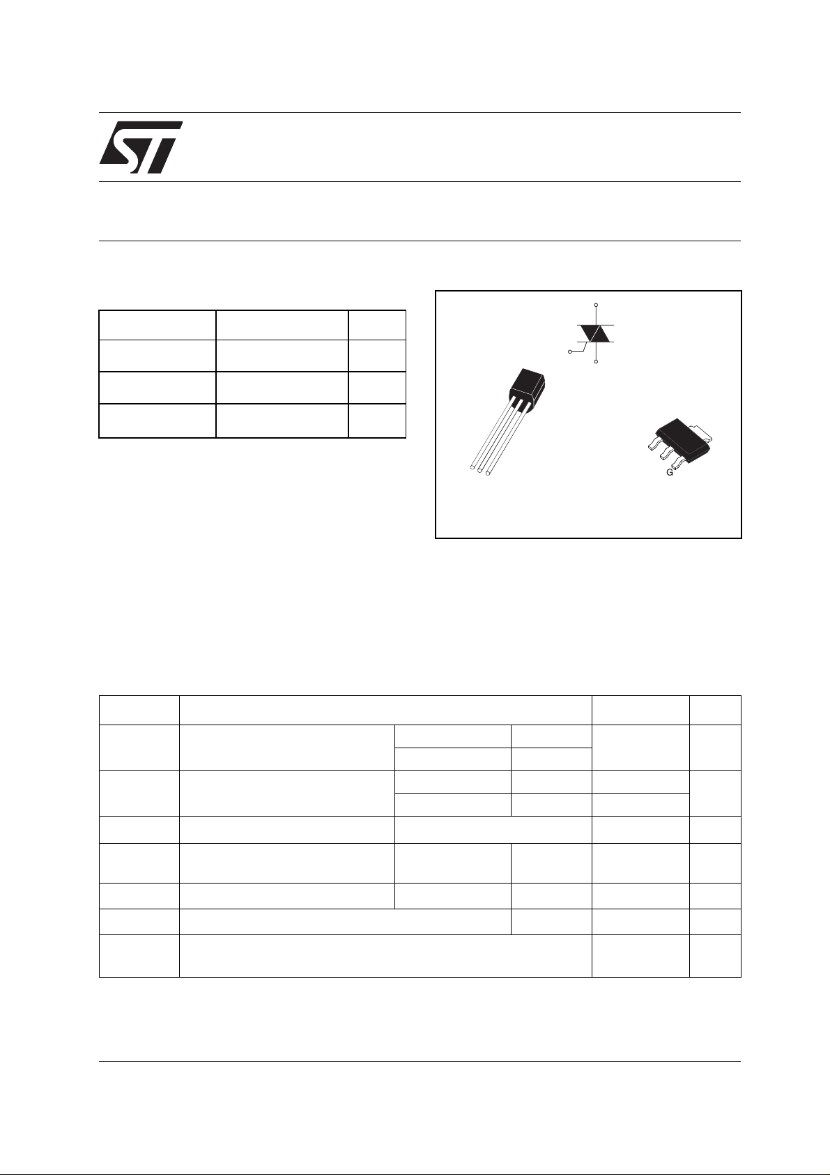
A1
G
A2
TO-92
(Z01xxA)
A2
G
A1
A2
A1
A2
SOT-223
(Z01xxN)
ABSOLUTE MAXIMUM RATINGS
Symbol Parameter Value Unit
I
T(RMS)
I
TSM
²
I
dI/dt
I
GM
P
G(AV)
T
stg
T
July 2003 - Ed: 5
RMS on-state current (full sine wave) SOT-223 Ttab = 90°C
TO-92 TI = 50°C
Non repetitive surge peak on-state
current (full cycle, Tj initial = 25°C)
tI
²
t Value for fusing
Critical rate of rise of on-state current
I
= 2 x IGT , tr ≤ 100 ns
G
F = 50 Hz t = 20 ms 8 A
F = 60 Hz t = 16.7 ms 8.5
tp = 10 ms 0.35
F = 120 Hz Tj = 125°C 20 A/µs
Peak gate current tp = 20 µs Tj = 125°C 1 A
Average gate power dissipation Tj = 125°C 0.1 W
Storage junction temperature range
Operating junction temp erature range
j
- 40 to + 150
- 40 to + 125
1
A
A
°C
²
s
1/7
Z01 Series
ELECTRICAL CHARACTERISTICS (Tj = 25°C, unless otherwise specified)
Symbol Test Conditions Quadrant Z01xx
03 07 09 10
I
GT
I
H
(1)
V
= 12 V RL = 30 Ω
V
GT
V
GD
(2)
I
L
D
VD = V
DRM
= 50 mA
I
T
IG = 1.2 I
RL = 3.3 kΩ Tj = 125°C
GT
I - II - III
IV
MAX.
3
5
5
10
7
10
25
25
ALL MAX. 1.3 V
ALL MIN. 0.2
MAX. 7 10 10 25 mA
I - III - IV MAX. 7 10 15 25 mA
II 15 20 25 50
dV/dt (2) V
= 67 %V
D
(dV/dt)c (2) (dI/dt)c = 0.44 A/ms
gate open Tj = 110°C
DRM
Tj = 110°C MIN. 0.5 1 2 5 V/µs
MIN. 10 20 50 100 V/µs
STATIC CHARACTERISTICS
Symbol Test Conditions Value Unit
(2) ITM = 1.4 A tp = 380 µs
V
TM
(2)
V
to
R
(2)
d
I
DRM
I
RRM
Note 1: minimum IGT is guaranted at 5% of IGT max.
Note 2: for both polarities of A2 referenced to A1
Threshold voltage Tj = 125°C MAX. 0.95 V
Dynamic resistance Tj = 125°C MAX. 400 mΩ
V
= V
DRM
RRM
Tj = 25°C MAX. 1.6 V
Tj = 25°C
Tj = 125°C 0.5 mA
MAX.
5µA
Unit
mA
V
THERMAL RESISTANCES
Symbol Parameter Value Unit
R
th(j-t)
R
th(j-l)
R
th(j-a)
S = Copper surface under tab
Junction to tab (AC)
Junction to lead (AC)
Junction to ambient
S = 5 cm
SOT-223 25
TO-92 60
²
SOT-223 60
TO-92 150
°C/W
°C/W
2/7
PRODUCT SELECTOR
Z01 Series
Part Number
Voltage
Sensitivity Type
Package
600 V 700 V 800 V
Z0103MA X 3 mA Standard TO-92
Z0103MN X 3 mA Standard SOT-223
Z0103SA X 3 mA Standard TO-92
Z0103SN X 3 mA Standard SOT-223
Z0103NA X 3 mA Standard TO-92
Z0103NN X 3 mA Standard SOT-223
Z0107MA X 5 mA Standard TO-92
Z0107MN X 5 mA Standard SOT-223
Z0107SA X 5 mA Standard TO-92
Z0107SN X 5 mA Standard SOT-223
Z0107NA X 5 mA Standard TO-92
Z0107NN X 5 mA Standard SOT-223
Z0109MA X 10 mA Standard TO-92
Z0109MN X 10 mA Sta ndar d SOT-223
Z0109SA X 10 mA Standard TO-92
Z0109SN X 10 mA Standar d SOT-223
Z0109NA X 10 mA Standard TO-92
Z0109NN X 10 mA Standard SOT-22 3
Z0110MA X 25 mA Standard TO-92
Z0110MN X 25 mA Sta ndar d SOT-223
Z0110SA X 25 mA Standard TO-92
Z0110SN X 25 mA Standar d SOT-223
Z0110NA X 25 mA Standard TO-92
Z0110NN X 25 mA Standard SOT-22 3
ORDERING INFORMA T IO N
Z 01 03 M A 1AA2
TRIAC
SERIES
CURRENT: 1A
SENSITIVITY:
03: 3mA
07: 5mA
09: 10mA
10: 25mA
VOLTAGE:
M: 600V
S: 700V
N: 800V
Blank
PACKAGE:
A:TO-92
N: SOT-223
PACKING MODE:
1AA2:TO-92 bulk (preferred)
2AL2:TO-92 ammopack
5AA4: SOT-223Tape & reel
3/7

Z01 Series
OTHER INFORMATION
Part Number Marking Weight
Base
quantity
Packing
mode
Z01xxyA 1AA2 Z01x xyA 0.2 g 2500 Bulk
Z01xxyA 2AL2 Z01xxyA 0.2 g 2000 Ammopack
Z0103yN 5AA4 Z3y 0.12 g 1000 Tape & reel
Z0107yN 5AA4 Z7y 0.12 g 1000 Tape & reel
Z0109yN 5AA4 Z9y 0.12 g 1000 Tape & reel
Z0110yN 5AA4 Z0y 0.12 g 1000 Tape & reel
Note: xx = sensitivity, y = voltage
Fig. 1: Maximum power dissipation versus RMS
on-state current (full cycle).
P(W)
1.50
1.25
1.00
0.75
0.50
0.25
0.00
0.0 0.1 0.2 0.3 0.4 0.5 0.6 0.7 0.8 0.9 1.0
IT(RMS)(A)
Fig. 2-1: RMS on-state current versus ambient
temperature (full cycle).
IT(RMS)(A)
1.2
1.0
0.8
0.6
TO-92
(Rth(j-a=Rth(j-l))
0.4
0.2
0.0
0 25 50 75 100 125
Tl orTtab (°C)
SOT-223
(Rth(j-a)=Rth(j-t))
Fig. 2-2: RMS on-state current versus ambient
temperature (fu l l cycle ).
IT(RMS)(A)
1.2
1.0
0.8
0.6
TO-92
0.4
Rth(j-a)=150°C/W
0.2
0.0
0 25 50 75 100 125
4/7
SOT-223
(Rth(j-a)=60°C/W)
Tamb(°C)
Fig. 3: Relative variation of thermal impedance
junction to ambient versus pulse duration.
K=[Zth(j-a)/Rth(j-a)]
1.00
Z01xxxA
0.10
Z01xxxN
0.01
1E-3 1E-2 1E-1 1E+0 1E+1 1E+2 5E+2
tp(s)

Z01 Series
Fig. 4: Relative variation of gate trigger current,
holding current and latching current versus
junction temperature (typical values).
IGT,IH,IL [Tj] / IGT,IH,IL [Tj=25°C]
2.5
2.0
IGT
1.5
IH & IL
1.0
0.5
Tj(°C)
0.0
-40 -20 0 20 40 60 80 100 120 140
Fig. 6: Non-repetitive surge peak on-state
current for a sinusoidal pulse with width
tp < 10ms, and corresponding value of I²t.
ITSM (A), I²t (A²s)
100.0
10.0
dI/dt limitation:
20A/µs
Tj initial=25°C
ITSM
Fig. 5: Surge peak on-state current versus
number of cycles.
ITSM(A)
9
8
7
6
Non repetitive
Tj initial=25°C
t=20ms
One cycle
5
4
3
Repetitive
Tamb=25°C
2
1
0
1 10 100 1000
Number of cycles
Fig. 7: On-state characteristics (maximum
values).
ITM(A)
10.0
Tj=Tj max.
1.0
1.0
I²t
tp (ms)
0.1
0.01 0.10 1.00 10.00
Fig. 8: Relative variation of critical rate of
decrease of main current versus (dV/dt)c (typical
values).
(dI/dt)c [(dV/dt)c] / Specified (dI/dt)c
2.6
2.4
2.2
2.0
1.8
1.6
1.4
1.2
1.0
0.8
0.6
0.4
0.2
0.0
0.1 1.0 10.0 100.0
Z0103
Z0107
(dV/dt)c (V/µs)
Z0109
Z0110
Tj=25°C
VTM(V)
0.1
0.0 0.5 1.0 1.5 2.0 2.5 3.0 3.5 4.0 4.5 5.0
Tj max.
Vto= 0.95 V
Rd= 420 m
Ω
Fig. 9: Relative variation of critical rate of
decrease of main current versus junction
temperature.
(dI/dt)c [Tj] / (dI/dt)c [Tj specified]
6
5
4
3
2
1
0
0 25 50 75 100 125
Tj (°C)
5/7

Z01 Series
Fig. 10: SOT-223 Therm al resistance junction t o
ambient versus copper surface under tab (printed
circuit board FR4, copper thickness: 35µm).
Rth(j-a) (°C/W)
130
120
110
100
90
80
70
60
50
40
30
20
10
0
0.0 0.5 1.0 1.5 2.0 2.5 3.0 3.5 4.0 4.5 5.0
S(cm²)
SOT-223
PACKAGE MECHANICAL DATA
SOT-223 (Plastic)
A
A1
B
e1
D
B1
H
E
e
V
DIMENSIONS
c
REF.
Millimeters Inches
Min. Typ. Max. Min. Typ. Max.
A 1.80 0.071
A1 0.02 0.1 0.0008 0.004
B 0.60 0.70 0.85 0.024 0.027 0.034
B1 2.90 3 .00 3.15 0.114 0.118 0.124
c 0.24 0 .26 0.35 0. 009 0.010 0. 014
D 6.30 6 .50 6.70 0. 248 0.256 0. 264
e 2.3 0.09 0
e1 4.6 0.18 1
E 3.30 3.50 3.70 0.130 0.138 0.146
H 6.70 7 .00 7.30 0. 264 0.276 0. 287
V 10° max
6/7

FOOTPRI NT DIME NSIO NS (in millimeters )
SOT-223 (Plastic)
PACKAGE MECHANICAL DATA
TO-92 (Plastic)
Z01 Series
DIMENSIONS
REF .
a
Millimeters Inches
Min. Typ. Max. Min. Typ. Max.
A 1.35 0.053
BAC
B 4.70 0.185
C 2.54 0.100
D 4.40 0.173
F
D
E
E 12.70 0.500
F 3.70 0.146
a 0.45 0.017
Information furnished is believed to be accurate and reliable. However, STMicroelectronics assumes no responsibility for the consequences
of use of su ch in for mat i on n or f or a ny in fr ing em ent of pa te nts or o ther r igh ts of th ir d pa r tie s w hic h may res ul t f rom i ts us e. No license is granted
by impl i cation or ot herwise under any patent or patent r i ght s of STMi croelectro ni cs. Specif i cations mentioned i n this publ i cation are subje ct
to change wi t hout notice. T hi s publicati on supersede s and replaces all in formation previously supplied. STM i croelectro ni cs products are not
authori zed for use as cr i tical compo nents in life support devices or systems without ex press written approva l o f ST M i croelectr o nics.
© The ST logo is a registered trademark of STMicroelectronics
© 2003 STMicroelectronics - Printed in Italy - All Rights Reserved
STMicroele ct ronics GROUP OF COM PANIES
Australi a - Brazil - Chi na - Finland - F rance - Germ any - Hong Kon g - India - Italy - Japan - Malaysia
Malta - Mor occo - Singapore - Spain - S weden - Switzerland - United Kingdom - U.S.A
http://w ww.st.com
7/7
 Loading...