

Z00607MA
Z00607DA
®
May 1999 - Ed: 1
SENSITIVE GATE TRIACS
Symbol Parameter Value Unit
I
T(RMS)
RMS on-state current
(360° conduction angle)
Tl= 50 °C0.8 A
I
TSM
Non repetitive surge peak on-state current
(T
j
initial = 25°C )
tp = 8.3 ms 10.5 A
tp = 10 m s 10
Non repetitive surge peak on-state current
(T
j
initial = 110°C, full cycle)
F = 60Hz 8
I
2
t
I
2
t Value for fusing
tp = 10 m s 0.5 A
2
s
T
stg
T
j
Storage and operating junction temperature range
- 40, + 150
- 40, + 110
°
C
Tl Maximum lead temperature for soldering during 10s 260
°
C
ABSOLUTE RATINGS
(limiting values)
I
T(RMS)
= 0.8A
V
DRM
= 400V and 600V
IGT = 5mA
FEATURES
Symbol Parameter
Z00607xA
Unit
DM
V
DRM
V
RRM
Repetitive peak off-state voltage
T
j
= 110°C
400 600 V
The Z006607xA triacs are intended for general
applications where high gate sensitivity is
required.
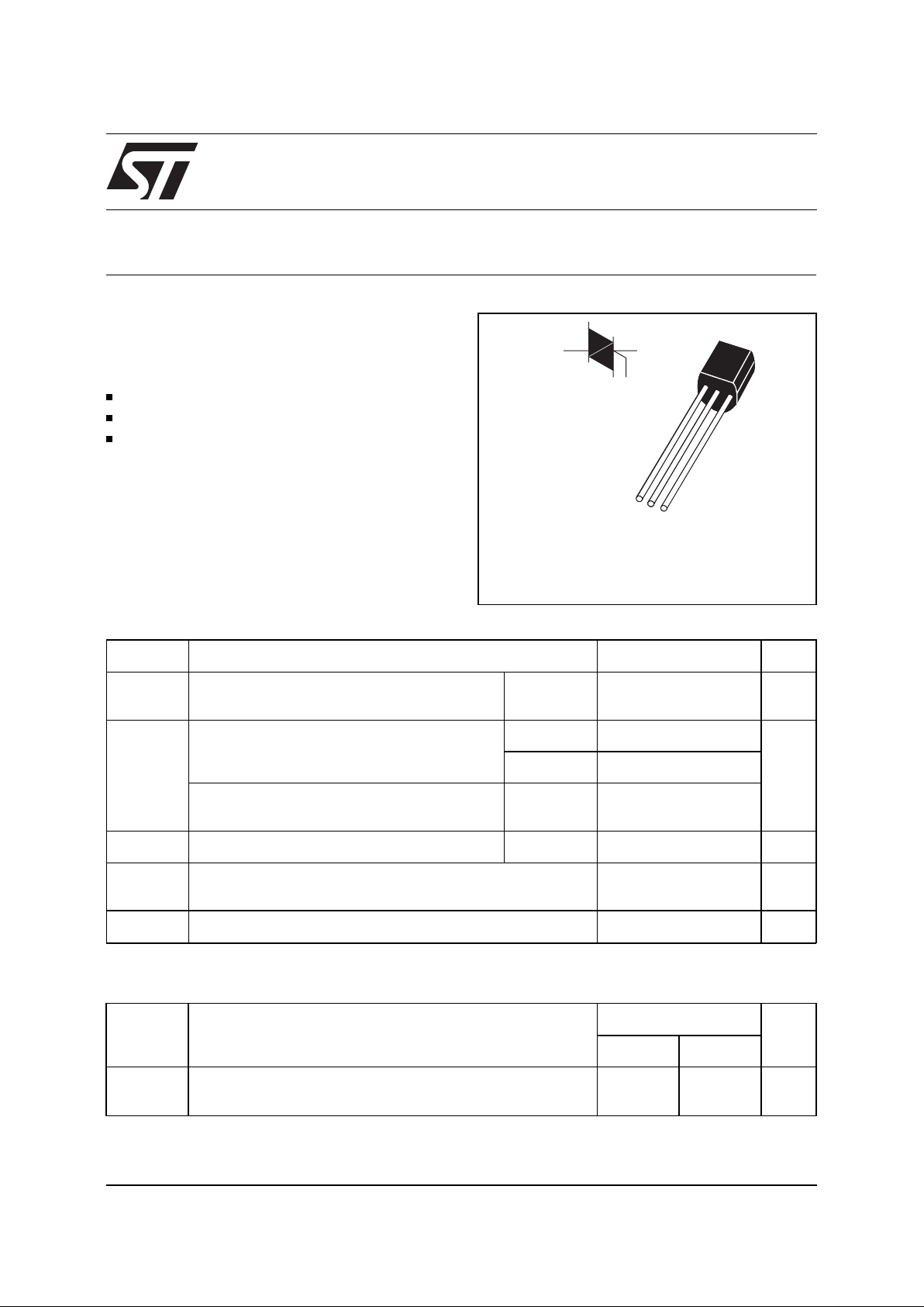
DESCRIPTION
A1
A2
G
A2
A1
G
TO92
(Plastic)
1/4

P
G (AV)
= 0.1 W PGM = 2 W (tp = 20 µs) IGM = 1 A (tp = 20 µs)
GATE CHARACTE RIST ICS
(maximum values)
Symbol Parameter Value Unit
Rth(j-a) Junction to ambient 150
°
C/W
Rth(j-l) Junction to lead 60
°
C/W
THERMAL RE SISTA NC ES
Symbol Test Conditions Quadrant
Sensitivity
Unit
07
I
GT
VD=12V (DC) RL=140
Ω
Tj= 25°C I-II-III MAX 5 mA
IV MAX 7
V
GT
VD=12V (DC) RL=140
Ω
Tj= 25°C I-II-III-IV MAX 1.5 V
V
GD
VD=V
DRM
RL=3.3kΩ
Tj= 110°C I-II-III-IV MIN 0.2 V
tgt V
D=VDRM
IG = 25mA
I
T
= 1.0A
dI
G
/dt = 0.25A/µs
Tj= 25°C I-II-III-IV TYP 2
µ
s
I
H
*I
T
= 200 mA Gate open Tj= 25°CMAX5mA
I
L
I
G
= 1.2 I
GT
Tj= 25°C I-III-IV MAX 10 mA
II MAX 20
V
TM
*ITM= 1.1A tp= 380µs T j= 25°CMAX1.5V
I
DRM
I
RRM
VD = V
DRM
VR = V
RRM
Tj= 25°CMAX10
µ
A
Tj= 110°CMAX0.1mA
dV/dt * VD=67%V
DRM
Gate open
Tj= 110°CMIN10V/
µ
s
(dV/dt)c *
(dI/dt)c = 0.35 A/ms
Tj= 110°CMIN1.5V/
µ
s
* For either polarity of electrode A
2
voltage with reference to electrode A
1
ELECTRICAL CHARACT E RISTICS
0.0 0.1 0.2 0.3 0.4 0.5 0.6 0.7 0.8
0.0
0.1
0.2
0.3
0.4
0.5
0.6
0.7
0.8
0.9
1.0
P(W)
α=180°
α=120°
α=90°
α=60°
α=30°
IT(RMS)(A)
180°
α
α
Fig 1:
Maximum power dissipation versus RMS
on-state current.
0 102030405060708090100110
0.0
0.1
0.2
0.3
0.4
0.5
0.6
0.7
0.8
0.9
1.0
P(W) Tlead (°C)
Rth(j-a)
Rth(j-l)
α=180°
110
50
70
90
Tamb(°C)
Fig 2:
Correlation between maximum power dissipation and maximum allowable temperatures
(Tamb and Tlead).
Z00607DA / Z00607MA
2/4

12 510
0.1
1.0
10.0
50.0
ITSM(A),I²t(A²s)
Tj initial=25°C
ITSM
I²t
tp(ms)
Fig 7:
Non repetitive surge peak on-state current
for a sinusoidal pulse with width tp<10ms, and c orresponding value of I
2
t.
0.0 0.5 1.0 1.5 2.0 2.5 3.0 3.5 4.0 4.5 5.0
0.1
1.0
10.0
ITM(A)
Tj=25°C
Tj max.:
Vto= 0.95 V
Rd= 420 mΩ
Tj=Tj max.
VTM(V)
Fig 8:
On-state characteristics (maximum values).
-40 -20 0 20 40 60 80 100 120
0.0
0.5
1.0
1.5
2.0
2.5
IGT,IH[Tj] / IGT,IH[Tj=25°C]
IGT
IH
Tj(°C)
Fig 5:
Relative variation of gate trigger current and
holding current versus junction temperature (typical values).
1 10 100 1000
0
1
2
3
4
5
6
7
8
9
ITSM(A)
Tj initial=25°C
F=50Hz
Number of cycles
Fig 6:
Non repetitive surge peak on-state current
versus number of cycles.
0 102030405060708090100110
0.0
0.1
0.2
0.3
0.4
0.5
0.6
0.7
0.8
0.9
1.0
IT(RMS)(A)
α=180°
Rth(j-a)=Rth(j-l)
Rth(j-a)=150°C/W
Tamb(°C)
Fig 3:
RMS on-state current versus ambient temperature.
1E-3 1E-2 1E- 1 1E+0 1E+1 1E+2 5E+2
0.01
0.10
1.00
K=[Zth(j-a)/Rth(j-a)]
tp(s)
Fig 4:
Relative variation of thermal impedance
junction to ambient versus pulse duration.
Z00607DA / Z00607MA
3/4

Information furnished is believed to be accurate and reliable. However, STMicroelectronics assumes no responsibility for the consequences of
use of such information nor for any infringement of patents or other rights of third parties which may result from its use. No license is granted by
implication or otherwis e under any patent or patent rights of STMicroelectro nics. Specifications men tioned in this publication are subject to
change without notice. This publication supersedes and replaces all information previously supplied.
STMicroelectro nic s products are not authorized for use as critical components in l i fe s upport devices or systems wi thout express writt en approval of STMicroelectronics.
The ST logo is a registered trademark o f STMicroelectron ics
© 1999 STMicroelectronics - Printed in Italy - All rights reserved.
STMicroelectronics GROUP OF COMPANIES
Australia - Brazil - Canada - China - France - Germany - Italy - Japan - Korea - Malaysia - Malta - Mexico - Morocco -
The Netherlands - Singapore - Spain - Sweden - Switzerland - Taiwan - Thailand - United Kingdom - U.S.A.
http://www.st.com
PACKAGE ME CHANICAL D AT A
TO92 (Plastic)
D
F
a
E
BAC
REF.
DIMENSIONS
Millimeters Inches
Typ. Min. Max. Typ. Min. Max.
A1.35 0.053
B 4.70 0.185
C2.54 0.100
D 4.40 0.173
E 12.70 0.500
F 3.70 0.146
a 0.45 0.017
Ordering type Marking Package Weight Base qty Delivery mode
Z00607DA 1BA2 Z0607DA TO92 0.2g. 2500 Bulk
Z00607MA 1BA2 Z0607MA TO92 0.2g. 2500 Bulk
Z00607DA / Z00607MA
4/4
 Loading...