

SGS Thomson Microelectronics VND810MSP Datasheet
®
VND810 MS P
DOUBLE CHANNEL HIGH SIDE DRIVER
TYPE R
DS(on)
I
OUT
V
CC
VND810 M SP 150 mΩ (*) 0.6 A (*) 36 V
(*) Per each channel
■ CMOS COMPATIBLE INPUTS
■ OPEN DRAIN STATUS OUTPUTS
■ ON STATE OPEN LOAD DETECTION
■ OFF STATE OPEN LOAD DETECTION
■ SHORTED LOAD PROTECTION
■ UNDERVOLTAGE AND OVERVOLTAGE
SHUTDOWN
■ PROTECTION AGAINST LOSS OF GROUND
■ VERY LOW STAND-BY CURRENT
■ REVERSE BATTERY PROTECTIO N (**)
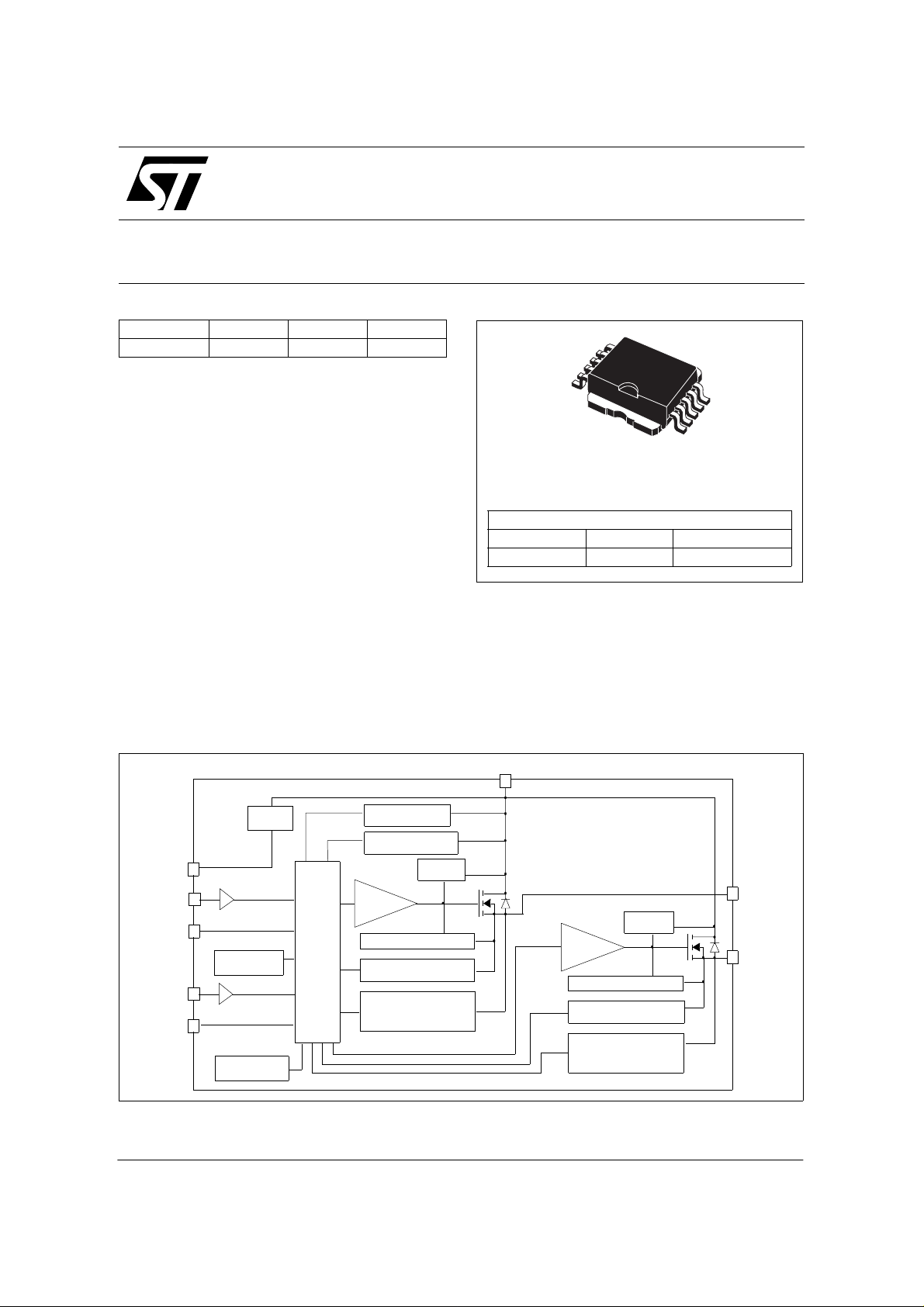
DESCRIPTION
The VND810MSP is a monolithic device designed
in STMicroelectronics VIPower M0-3 Technology,
intended for driving any kind of load with one side
connected to ground.
Active VCC pin voltag e clamp protects th e dev ice
against low energy spikes (see ISO7637 transient
compatibility table). Active current limitation
BLO C K DIAG RA M
10
1
PowerSO-10
™
ORDER CODES
PACKAGE TUBE T&R
PowerSO-1 0™ VND810MSP VND810MSP13TR
combined with thermal shutdown and automatic
restart protects the device against overloa d. The
current limitati on threshold is aimed at d etecting
the 21W/12V sta ndard bulb as an o verload fault.
The device detects open load condition both in on
and off state. Output shorted to VCC is detected in
the off state. Device automatically turns off in case
of ground pin disconnection.
V
cc
V
cc
CLAMP
GND
INPUT1
STATUS1
OVERTEMP. 1
INPUT2
STATUS2
OVERTEMP. 2
(**) See appl ic ation schema tic at page 8
LOGIC
OVERVO LTAGE
UNDERVOLTAGE
CLAMP 1
DRIVER 1
CURRENT LIMITER 1
OPENLOAD ON 1
OPENLOAD OFF 1
CLAMP 2
DRIVER 2
CURRENT LIMITER 2
OPENLOAD ON 2
OPENLOAD OFF 2
OUTPUT1
OUTPUT2
July 2002 1/18
1
VND810MSP
ABSOLUTE MAXIMUM RATI NG
Symbol Parameter Value Unit
tot
DC Supply Voltage 41 V
Reverse DC Supply Voltage - 0.3 V
CC
DC Reverse Ground Pin Current - 200 mA
DC Output Current Internally Limited A
Reverse DC Output Current - 6 A
DC Input Current +/- 10 mA
DC Status Cur rent +/- 10 mA
Electros tatic Discharge (Hum an Body Model: R=1.5KΩ; C=100pF)
- INPUT
- STATUS
- OUTPU T
- V
CC
Maximum Switching Energy
(L=400mH; R
=0Ω; V
L
=13.5V; T
bat
=150ºC; IL=0.9A)
jstart
4000
4000
5000
5000
225 mJ
Powe r Dissipation TC=25°C 52 W
Junction Operating Temperature Internally Limited °C
j
Case Operating Temperature - 40 to 150 °C
c
Storage Temperature - 55 to 150 °C
V
CC
- V
- I
GND
I
OUT
- I
OUT
I
IN
I
stat
V
ESD
E
MAX
P
T
T
T
stg
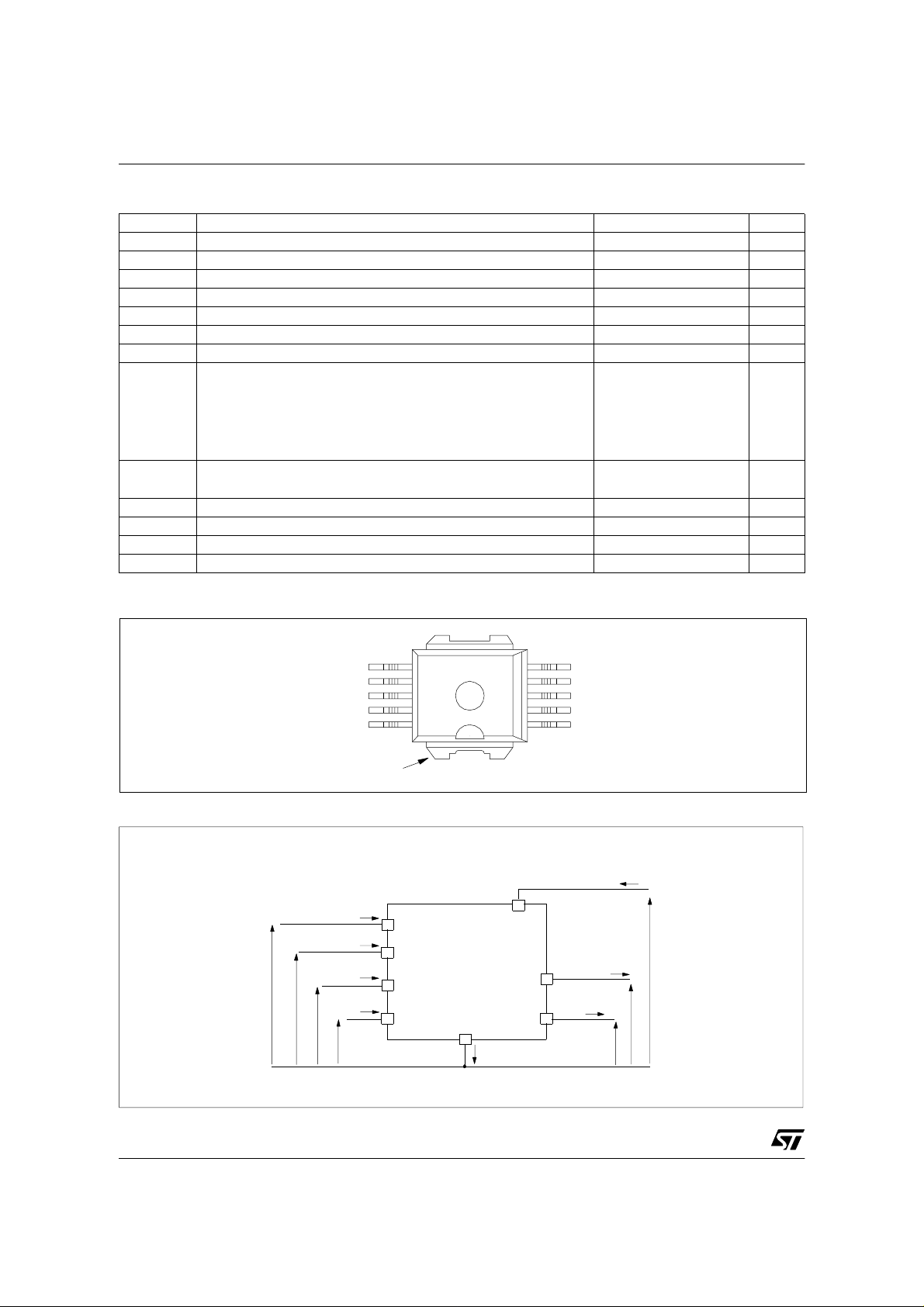
CONNECTION DIAGRAM (TOP VIEW)
V
V
V
V
GROUND
INPUT 1
STATUS 1
STA TUS 2
INPUT 2
V
CC
CURRENT AND VOLTAGE CO NVENTIONS
I
IN1
STAT1
V
I
I
I
IN2
V
STAT2
V
IN1
V
INP UT 1
STAT1
STATUS 1
IN2
INPUT 2
STAT2
STATUS 2
6
7
8
9
10
11
GND
5
4
3
2
1
V
CC
OUTPUT 1
OUTPUT 2
I
GND
OUTPUT 1
OUTPUT 1
N.C.
OUTPUT 2
OUTPUT 2
I
OUT2
V
OUT2
I
OUT1
V
OUT1
I
S
V
CC
2/18
1
VND810MSP
THERMAL DATA
Symbol Parameter Value Unit
R
thj-case
R
thj-amb
(*) When mounted on a standard single-sided FR-4 board with 0.5cm2 of Cu (at least 35µm thick). Horizontal mounting and no artificial air
flow.
ELECTRICAL CHARACTERISTICS (8V<VCC<36V; -40°C < Tj <150°C, unless otherwise specified)
(Per each channel)
POWER OUTPUTS
Symbol Parameter Test Conditions Min Typ Max Unit
V
CC
V
USD
V
OV
R
ON
I
S
I
L(off1)
I
L(off2)
I
L(off3)
I
L(off4)
(**) Per device
SWITCHING (VCC=13V)
Symbol Parame ter Test Condit ions Min Typ Max Unit
t
d(on)
t
d(off )
dV
OUT
dt
(on)
dV
OUT
dt
(off)
Thermal R esistanc e Junctio n-case 2.4 °C/W
Thermal Resistance Junctio n-ambient 52.4 (*) °C/W
(**) Operating Supply Voltage 5.5 13 36 V
(**) Undervoltage Shut -down 3 4 5.5 V
(**) Overvoltage Shut-down 36 V
On State Resistance
(**) Supply Current
Off State Output Curr ent VIN=V
Off State Output Curr ent VIN=0V; V
Off State Output Curr ent VIN=V
Off State Output Curr ent VIN=V
Turn-on Delay Time
Turn-off Delay Time
/
Turn-on Voltage Slope
/
Turn-off Voltage Slope
=0.5A; Tj=25°C
I
OUT
I
=0.5A; VCC>8V
OUT
Off State; V
Off State; V
=13V; VIN=V
CC
=13V; VIN=V
CC
OUT
OUT
Tj=25°C
On State; V
RL=13Ω from VIN rising edge to
V
=1.3V
OUT
RL=13Ω from VIN falling edge to
V
=11.7V
OUT
RL=13Ω from V
V
=10.4V
OUT
RL=13Ω from V
V
=1.3V
OUT
=13V; VIN=5V; I
CC
=0V 0 50 µA
OUT
=3.5V -75 0 µA
OUT
=0V; Vcc=13V; Tj =125°C 5 µA
OUT
=0V; Vcc=13V; Tj =25°C 3 µA
OUT
=1.3V to
OUT
=11.7V to
OUT
OUT
=0V
=0V;
=0A
12
12
30 µs
30 µs
See
relative
diagram
See
relative
diagram
150
320
40
25
5
7
mΩ
mΩ
µA
µA
mA
V/µs
V/µs
LOGIC INPUT
Symbol Param eter Test Conditions Min Typ Max Unit
Input Low Level 1.25 V
IL
Low Level Input Current VIN = 1.25V 1 µA
IL
Input High Level 3.25 V
IH
High Level Input Curr ent VIN = 3.25V 10 µA
Input Hyst eresis Vo lt age 0.5 V
I
Input Clamp Voltage
= 1mA
IN
I
= -1mA
IN
66.8
-0.7
8V
V
V
V
I
V
I
IH
I(hyst)
ICL
V
3/18
1
VND810MSP
ELECTRICAL CHARACTERISTICS (continued)
STATUS PIN
Symbol Parameter Test Conditions Min Typ Max Unit
V
STAT
I
LSTAT
C
STAT
V
SCL
Status Low Output Voltage I
Status Leakage Current Normal Operation; V
Status Pin Input
Capacitance
Status Clamp Voltage
PROTECTIONS
Symbol Parame ter Test Condit ions Min Typ Max Unit
T
TSD
T
T
t
SDL
I
V
demag
hyst
lim
Shut-down Temperature 150 175 200 °C
Reset Temp erature 135 °C
R
Ther ma l Hy steresi s 7 15 °C
Status Delay in Overload
Conditions
Current limitation
Turn-off Output Clamp
Voltage
= 1.6 mA 0.5 V
STAT
Normal Operation; V
= 1mA
I
STAT
I
= - 1mA
STAT
Tj>T
TSD
= 5V 10 µA
STAT
= 5V 100 pF
STAT
66.8
-0.7
0.6 0.9 1.2
5.5V<V
I
OUT
<36V
CC
=0.5A; L=6mH VCC-41 VCC-48 VCC-55 V
8V
20 µs
1.2
V
A
A
OPENLOAD DETECTION
Symbol Parameter Test Conditions Min Typ Max Unit
I
OL
t
DOL(on)
V
t
DOL(off)
OPEN LOAD STATUS TIMING (with external pull-up)
V
INn
V
STAT n
Openload ON State
Detectio n Threshol d
Openload ON State
Detection Delay
=5V 20 40 80 mA
V
IN
=0A 200 µs
I
OUT
Openload OFF State
Voltage Detection
OL
Threshold
Openload Detection Delay
at Turn Off
V
OUT
t
DOL(off)
VIN=0V 1.5 2.5 3.5 V
> V
OL
I
OUT
t
DOL(on)
< I
OL
V
INn
V
STAT n
1000 µs
OVER TEMP STATUS TIMING
Tj > T
TSD
t
SDL
t
SDL
4/18
2
1
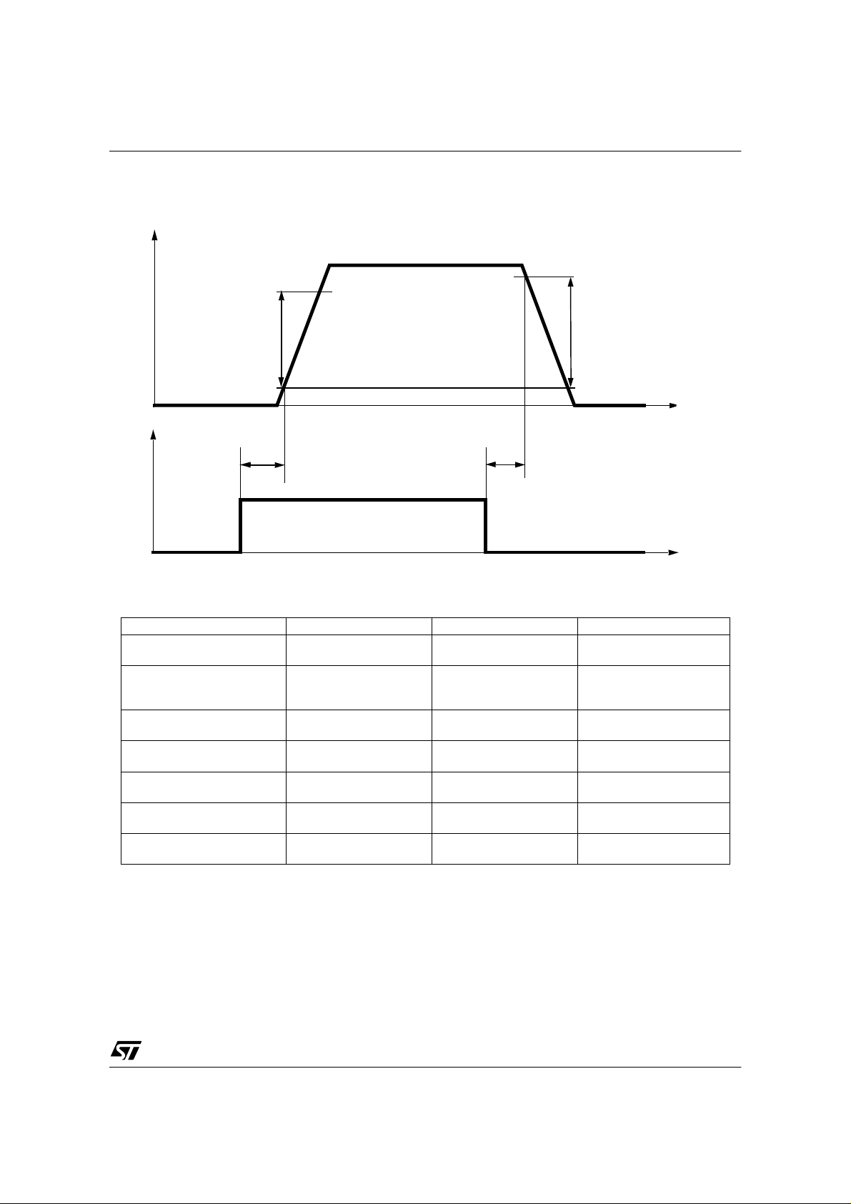
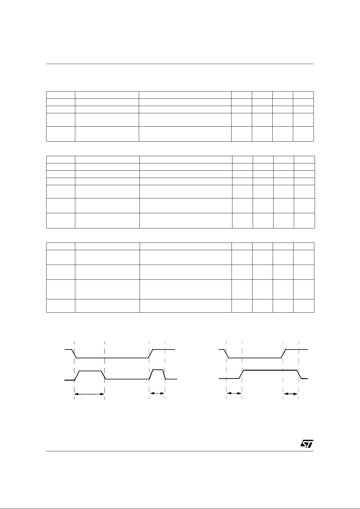
Switching time Waveforms
V
OUTn
dV
/dt
OUT
(on)
V
INn
t
d(on)
80%
10%
VND810MSP
90%
dV
/dt
OUT
(off)
t
td
(off)
t
TRUTH TABLE
CONDITIONS INPUT OUTPUT STATUS
Normal Ope ration
Current Limitation
Overtem peratur e
Undervoltage
Overvoltage
Output Voltage > V
Output Current < I
OL
OL
L
H
L
H
H
L
H
L
H
L
H
L
H
L
H
L
H
L
X
X
(T
(T
< T
j
> T
j
L
L
L
L
L
L
H
H
L
H
TSD
TSD
H
H
H
) H
) L
H
L
X
X
H
H
L
H
H
L
5/18
1
VND810MSP
ELECTRICAL TRANS IENT REQUIREMENTS ON VCC PIN
ISO T/R 7637/1
Test Pulse
1 -25 V -50 V -75 V -100 V 2 ms 10 Ω
2 +25 V +50 V +75 V +100 V 0.2 ms 10 Ω
3a -2 5 V -50 V -100 V -150 V 0.1 µs 50 Ω
3b + 25 V +50 V +75 V +100 V 0.1 µs 50 Ω
4 -4 V -5 V -6 V -7 V 100 ms, 0.01
5 +26.5 V +46.5 V +66.5 V +86.5 V 400 ms, 2
ISO T/R 76 37 / 1
Test Pulse
1CCCC
2CCCC
3aCCCC
3bCCCC
4CCCC
5CEEE
CLASS CONTENTS
C All functions of the device are perfo rmed as designed after exposure to disturbance .
E One or more functions of the dev ice is not performed as desig ned after exposure and cannot be
returned to prop er operat ion without replacing the devi ce.
I II III IV Delays and
I II III IV
TEST LEVELS
TEST LEVELS RESULTS
Impedance
Ω
Ω
6/18
1
1
 Loading...