VND600SP
DOUBLE CHANNEL HIGH SIDE SOLID STATE RELAY
TARGET SPECIFICATION
TYPE R
DS(on)
VND600SP 30mΩ 25A 36 V
■ DC SHORT CIRCUIT CURRENT: 25 A
■ CMOS COMPATIBLE INPUTS
■ PROPORTIONAL LOAD CURRENT SENSE
■ UNDERVOLTAGE AND OVERVOLTAGEn
SHUT-DOWN
■ OVERVOLTAGE CLAMP
■ THERMAL SHUT DOWN
■ CURRENT LIMITATION
■ VERY LOW STAND-BY POWER DISSIPATION
■ PROTECTION AGAINST:
n LOSS OF GROUND ANDLOSS OF V
■ REVERSE BATTERY PROTECTION (*)
DESCRIPTION
The VND600SP is a monolithic device made
using STMicroelectronics VIPower technology. It
is intended for driving resistive or inductive loads
with one side connectedtoground.ActiveV
voltage clamp protects the device against low
energy spikes (see ISO7637 transient
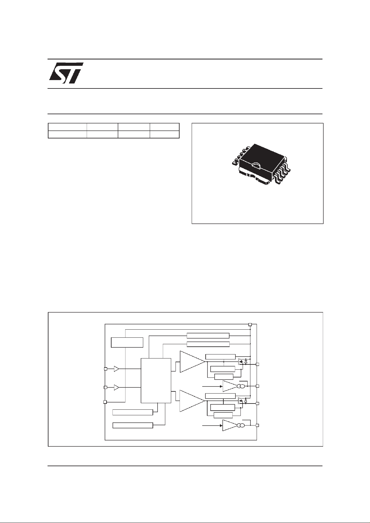
BLOCK DIAGRAM
I
lim
V
CC
10
1
PowerSO-10
CC
compatibility table). This device has two channels
in high side configuration; each channel has an
analog sense output on which the sensing current
is proportional (according to a known ratio) to the
corresponding load current. Built-in thermal shutdown and outputs current limitation protect the
chip from over temperature and short circuit.
Device turns off in case of ground pin
CC
pin
disconnection.
V
CC
OVERVOLTAGE
VCCCLAMP
INPUT 1
INPUT 2
GND
OVERTEMP.1
OVERTEMP. 2
(*) See application schematic at page7
LOGIC
Ot1
Ot2
UNDERVOLTAGE
DRIVER 1
I
OUT1
DRIVER2
I
OUT2
PwCLAMP 1
I
LIM1
V
dslim1
K
PwCLAMP 2
I
LIM2
V
dslim2
K
OUTPUT 1
Ot1
CURRENT
SENSE 1
OUTPUT 2
Ot2
CURRENT
SENSE 2
September 1999 1/10
1

VND600SP
ABSOLUTE MAXIMUM RATING
Symbol Parameter Value Unit
V
-V
-I
GND
I
OUT
I
I
V
CSENSE
V
ESD
P
TOT
T
T
T
STG
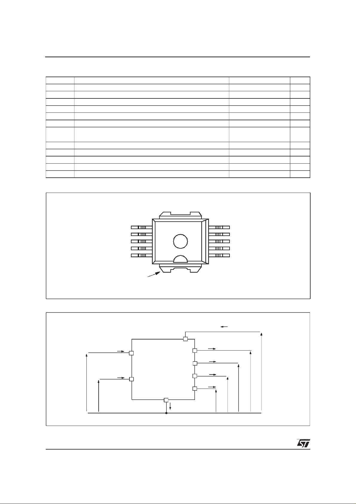
CONNECTION DIAGRAM (TOP VIEW)
DC supply voltage 41 V
CC
Reverse supply voltage -0.3 V
CC
DC reverse ground pin current -200 mA
Output current Internally limited A
Reverse output current -21 A
R
Input current +/- 10 mA
IN
Current sense maximum voltage
-3
+15
Electrostatic discharge (R=1.5kΩ; C=100pF) 2000 V
Power dissipation at Tc=25°C90W
Junction operating temperature Internally limited °C
j
Case operating temperature -40 to 150 °C
c
Storage temperature -55 to 150 °C
V
V
GROUND
INPUT 2
INPUT 1
C.SENSE1
C.SENSE2
10
V
CC
CURRENT ANDVOLTAGE CONVENTIONS
I
IN1
V
IN1
I
IN2
V
IN2
INPUT1
CURRENT SENSE 1
INPUT2
CURRENT SENSE 2
6
7
8
9
11
GROUND
V
CC
OUTPUT1
OUTPUT2
5
4
3
2
1
I
OUT1
I
SENSE1
I
OUT2
I
SENSE2
V
SENSE2
V
V
OUT2
I
CC
SENSE1
OUTPUT 2
OUTPUT 2
N.C.
OUTPUT 1
OUTPUT 1
V
OUT1
V
CC
2/10
1
I
GND

VND600SP
THERMAL DATA
Symbol Parameter Value Unit
R
R
Note: (1) one channel ON
ELECTRICAL CHARACTERISTICS (8V<VCC<36V; -40°C<Tj<150°C;unless otherwise specified)
(Per each channel)
POWER
(1) Thermal resistance junction-case (MAX) 1.75 °C/W
thj-case
(2) Thermal resistance junction-case (MAX) 1.2 °C/W
thj-case
R
thj-amb
(2) twochannels ON
Thermal resistance junction-ambient (MAX) 50 °C/W
Symbol Parameter Test Conditions Min Typ Max Unit
V
V
V
R
V
I
CC
USD
OV
ON
clamp
I
S
L(off)
Operating supply
voltage
5.5 13 36 V
Undervoltage shutdown 3 4 5.5 V
Overvoltage shutdown 36 42 48 V
I
OUT
On state resistance
Clamp voltage
I
OUT
I
OUT
=20 mA
I
CC
(see note 1)
Off state; Input n.c.; V
Supply current
On state; V
R
SENSE
Off state output current VIN=V
=5A; Tj=25°C
=5A; Tj=150°C
=3A; VCC=6V
41 48 55 V
=13V
CC
=5V; VCC=13V;I
IN
=3.9kΩ
=0V 0 50 µA
OUT
OUT
=0A;
30
60
100
40
6
mΩ
mΩ
mΩ
µA
mA
SWITCHING (VCC=13V)
Symbol Parameter Test Conditions Min Typ Max Unit
(dV
(dV
t
d(on)
t
d(off)
OUT
OUT
Turn-on delay time R1=2.6Ω 30 µs
Turn-on delay time R1=2.6Ω 30 µs
/dt)onTurn-on voltage slope R1=2.6Ω 0.20 V/µs
/dt)
Turn-off voltage slope R1=2.6Ω 0.20 V/µs
off
PROTECTIONS
Symbol Parameter Test Conditions Min Typ Max Unit
T
T
HYST
V
demag
V
I
lim
TSD
T
ON
=13V
V
DC short circuit current
CC
5.5V<VCC<36V
Thermal shut-down
temperature
Thermal reset
R
temperature
Thermal hysteresis 7 15 °C
=2A; VIN=0V; L=6mH
Turn-off output voltage
I
OUT
clamp
Output voltage drop
limitation
I
=0.5A
OUT
Tj= -40°C...+150°C
25 40 70
70
150 175 200 °C
135 °C
Vcc-41 Vcc-48 Vcc-55 V
50 mV
A
A
3/10
1
 Loading...