

Datasheet VNK10N06FM, VND10N06-1, VND10N06, VNP10N06FI Datasheet (SGS Thomson Microelectronics)
VND10N06/VND10N06-1
VNP10N06FI/K10N06FM
”OMNIFET”:
FULLY AUTOPROTECTED POWER MOSFET
TYPE V
VND10N06
VND10N06-1
VNP10N06FI
VNK10N06FM
■ LINEAR CURRENT LIMITATION
■ THERMALSHUTDOWN
■ SHORT CIRCUIT PROTECTION
■ INTEGRATEDCLAMP
■ LOW CURRENTDRAWNFROM INPUT PIN
■ LOGIC LEVEL INPUT THRESHOLD
■ ESD PROTECTION
■ SCHMITT TRIGGER ONINPUT
■ HIGH NOISE IMMUNITY
clamp
60 V
60 V
60 V
60 V
R
DS(on )
0.3 Ω
0.3 Ω
0.3 Ω
0.3 Ω
I
lim
10 A
10 A
10 A
10 A
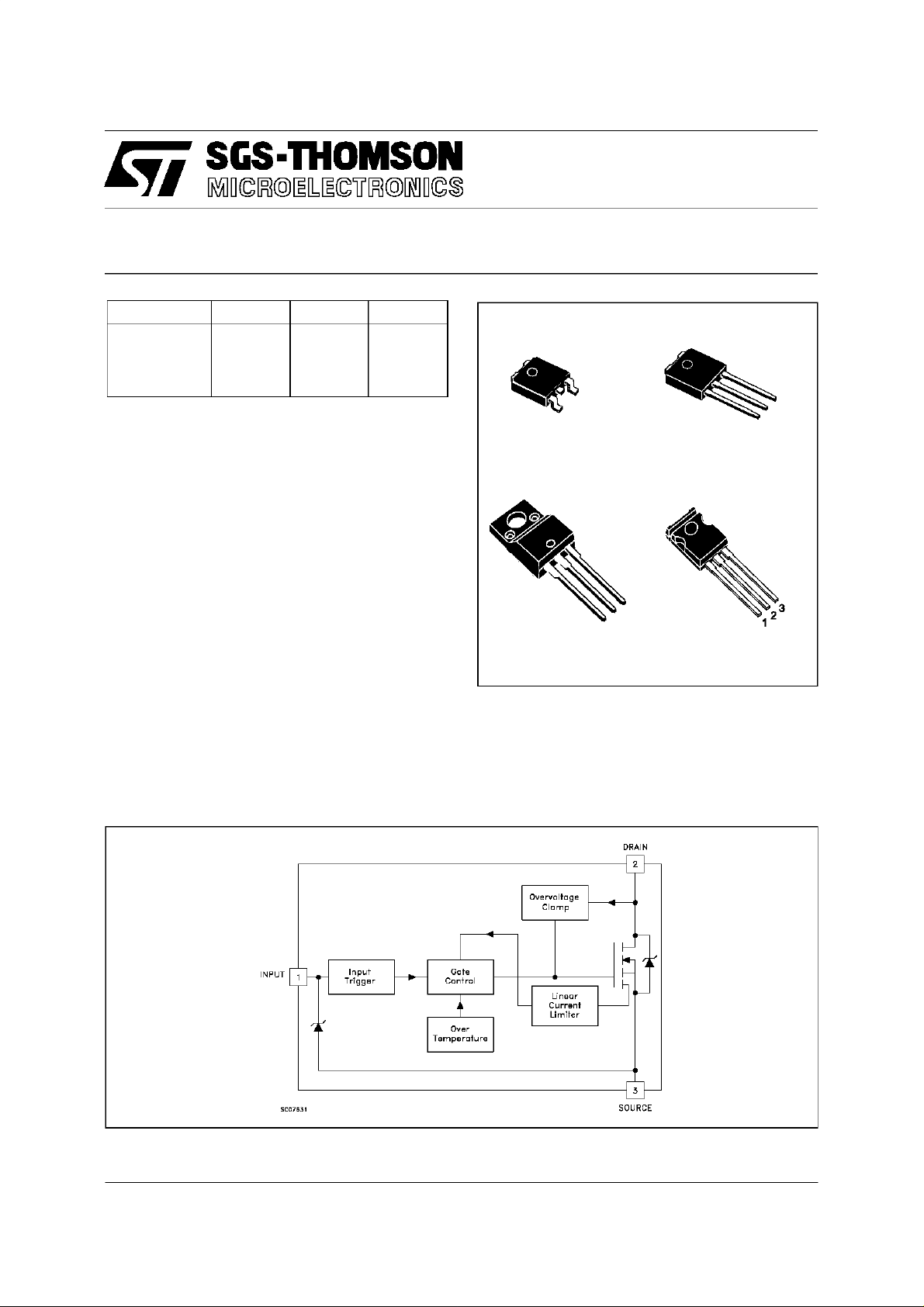
DESCRIPTION
The VND10N06, VND10N06-1, VNP10N06FIand
VNK10N06FM are monolithic devices made
using SGS-THOMSON Vertical Intelligent Power
M0 Technology, intended for replacement of
standard power MOSFETS in DC to 50 KHz
applications. Built-in thermal shut-down, linear
current limitation and overvoltage clamp protect
the chip in harshenviroments.
3
1
DPAK
TO-252
ISOWATT220
3
2
1
IPAK
TO-251
3
2
1
SOT82-FM
BLOCK DIAGRAM (*)
(∗) SOT82-FM Pin Configuration: INPUT= 3; SOURCE = 1; DRAIN = 2.
October 1997
1/14
VND10N06/VND10N06-1/VNP10N06FI/VNK10N06FM
ABSOLUTEMAXIMUM RATING
Symbol Parameter Value Unit
V
V
V
Drain-source Voltage ( Vin= 0) Int er nall y Clamped V
DS
Input V ol ta ge Int er nall y Clamped V
in
I
Input Current ± 20 mA
in
I
Drain Current Internally Limited A
D
I
Reverse DC Output Current -15 A
R
Elect r o st at ic Dischar ge ( C= 100 pF ,
esd
R=1. 5 KΩ)
P
T
Tot al Dis s ipation at Tc=25oC35279W
tot
T
Oper at i ng Junct ion T em perature Internally Limited
j
T
Case O perating T emp era tu r e Internally Limited
c
St orage Temperature -55 to 150
stg
THERMAL DATA
R
thj-case
R
thj-amb
Ther mal Resist an ce Juncti on-c ase
Max 3.5 4.5 14
Ther mal Resist an ce Juncti on-am b ient
Max 100 62.5 100
DPAK
IPAK
DPAK/IPAK ISOW ATT220 SOT82-FM
ISOWATT220 SOT82-FM
4000 V
o
o
o
C
o
C
o
C
C/W
C/W
ELECTRICAL CHARACTERISTICS (T
=25oC unless otherwise specified)
case
OFF
Symbol Parameter Test Conditions Min. Typ. Max. Unit
V
CLAMP
Drain-source Clamp
ID= 200 mA Vin= 0 50 60 70 V
Volt age
V
Input Low Lev el
IL
ID= 100 µAVDS=16V 1.5 V
Volt age
3.2 V
-1
8
-0.3
11
250
100
V
I
I
V
DSS
IH
INCL
ISS
Input High Level
Volt age
Input-Source Reverse
Clamp Voltage
Zer o Inpu t V olt ag e
Drain Current (V
in
=0)
Supply Current f rom
RL=27Ω VDD=16V
=0.5V
V
DS
Iin=-1mA
=1mA
I
in
V
=50V Vin=V
DS
VDS<35V Vin=V
IL
IL
VDS=0V Vin= 5 V 150 300 µA
Input Pin
ON (∗)
Symbol Parameter Test Conditions Min. Typ. Max. Unit
R
DS(on)
St at ic D rain- s our ce On
Resistance
Vin=7V ID=1A TJ< 125oC0.150.3Ω
V
V
µA
µA
2/14
VND10N06/VND10N06-1/VNP10N06FI/VNK10N06FM
ELECTRICAL CHARACTERISTICS (continued)
DYNAMIC
Symbol Parameter Test Conditions Min. Typ. Max. Unit
C
SWITCHING(**)
Symbol Parameter Test Conditions Min. Typ. Max. Unit
t
d(on)
t
d(off)
t
d(on)
t
d(off)
(di/dt)
Q
SOURCE DRAINDIODE
Out put Capacitance VDS=13V f=1MHz Vin= 0 350 500 pF
oss
Turn-on Delay Time
t
Rise T ime
r
Turn-off Delay Time
t
Fall T ime
f
Turn-on Delay Time
t
Rise T ime
r
Turn-off Delay Time
t
Fall T ime
f
Tur n-on Current Slope VDD=16V ID=1A
on
Total Input Charge VDD=12V ID=1A Vin=7V 13 nC
i
VDD=16V Id=1A
=7V R
V
gen
gen
=10Ω
(see figure 3)
VDD=16V Id=1A
=7V R
V
gen
=1000Ω
gen
(see figure 3)
=7V R
V
in
gen
=10Ω
1100
550
200
100
1.2
1
1.6
1.2
1.5 A/µs
1600
900
400
200
1.8
1.5
2.3
1.8
ns
ns
ns
ns
µs
µs
µs
µs
Symbol Parameter Test Conditions Min. Typ. Max. Unit
V
(∗)ForwardOnVoltage ISD=1A Vin=V
SD
t
rr
Reverse Recov ery
(∗∗)
Time
Reverse Recov ery
(∗∗)
Q
rr
I
= 1 A di/dt = 100 A /µs
SD
=30V Tj=25oC
V
DD
(see test circuit, figure 5)
IL
0.8 1.6 V
125
0.22
Charge
(∗∗)
I
RRM
Reverse Recov ery
3.5
Current
PROTECTION
Symbol Parameter Test Conditions Min. Typ. Max. Unit
I
lim
t
dlim
T
jsh
T
jrs
E
as
(∗) Pulsed: Pulse duration = 300 µs,duty cycle 1.5 %
(∗∗) Parameters guaranteed by design/characterization
Drain Cur rent Limit Vin=7V VDS=13V 6 10 15 A
(∗∗) St ep Res pon se
Vin=7V VDSstepfrom0to13V 12 20 µs
Current Lim it
(∗∗) Overtem perat ure
150
Shut dow n
(∗∗) Overtemper at u r e Reset 135
(∗∗) S i ngle Pulse
Avalanche Energy
starting Tj=25oCVDD=24V
=7V R
V
in
=1KΩ L=10mH
gen
250 mJ
ns
µC
A
o
o
C
C
3/14

VND10N06/VND10N06-1/VNP10N06FI/VNK10N06FM
PROTECTION FEATURES
During Normal Operation, the INPUT pin is
electrically connected to the gate of the internal
power MOSFET through a low impedance path
as soon asV
IN>VIH
.
The device then behaves like a standard power
MOSFET and can be used as a switch from DC
to 50KHz. The only difference from the user’s
standpoint is that a small DC current (typically
150 µA) flows into the INPUT pin in order to
supply the internal circuitry.
During turn-off of an unclamped inductive load
the output voltage is clamped to a safe level by
an integrated Zener clamp between DRAIN pin
and the gateof the internal Power MOSFET.
In this condition, the Power MOSFET gate is set
to a voltage high enough to sustain the inductive
load currenteven ifthe INPUTpin is drivento 0V.
The device integrates an active current limiter
circuit which limits the drain current I
to I
D
lim
whateverthe INPUTpin Voltage.
When the current limiter is active, the device
operatesin thelinear region, so powerdissipation
may exceed the heatsinking capability. Both case
and junction temperatures increase, and if this
phase lasts long enough, junction temperature
may reach the overtemperature thresholdT
If T
reaches T
j
, the device shuts down
jsh
jsh
.
whatever the INPUT pin voltage. The device will
restart automaticallywhen T
T
jrs
has cooled down to
j
4/14
VND10N06/VND10N06-1/VNP10N06FI/VNK10N06FM
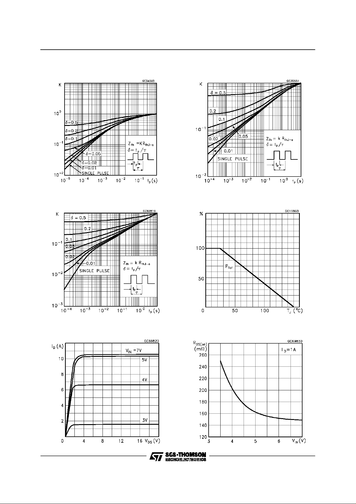
Thermal ImpedanceFor DPAK / IPAK
Thermal ImpedanceFor SOT82-FM
ThermalImpedanceFor ISOWATT220
DeratingCurve
OutputCharacteristics
StaticDrain-SourceOn Resistancevs Input
Voltage
5/14

VND10N06/VND10N06-1/VNP10N06FI/VNK10N06FM
StaticDrain-Source On Resistance
Input Chargevs InputVoltage
StaticDrain-SourceOn Resistance
CapacitanceVariations
Normalized Input Threshold Voltage vs
Temperature
6/14
Normalized On Resistance vs Temperature

VND10N06/VND10N06-1/VNP10N06FI/VNK10N06FM
Normalized On Resistance vs Temperature
Turn-onCurrent Slope
Turn-onCurrentSlope
Turn-off Drain-SourceVoltage Slope
Turn-offDrain-Source Voltage Slope
SwitchingTime ResistiveLoad
7/14

VND10N06/VND10N06-1/VNP10N06FI/VNK10N06FM
SwitchingTime Resistive Load
CurrentLimit vs JunctionTemperature
SwitchingTime ResistiveLoad
Step ResponseCurrent Limit
SourceDrain DiodeVoltage vs Junction
Temperature
8/14

VND10N06/VND10N06-1/VNP10N06FI/VNK10N06FM
Fig. 1: Unclamped Inductive Load Test Circuits
Fig. 3: SwitchingTimesTestCircuits For
ResistiveLoad
Fig. 2: UnclampedInductiveWaveforms
Fig. 4: InputCharge Test Circuit
Fig. 5: TestCircuit For InductiveLoad Switching
And Diode Recovery Times
Fig. 6: Waveforms
9/14

VND10N06/VND10N06-1/VNP10N06FI/VNK10N06FM
TO-252 (DPAK) MECHANICALDATA
DIM.
mm inch
MIN. TYP. MAX. MIN. TYP. MAX.
A 2.2 2.4 0.086 0.094
A1 0.9 1.1 0.035 0.043
A2 0.03 0.23 0.001 0.009
B 0.64 0.9 0.025 0.035
B2 5.2 5.4 0.204 0.212
C 0.45 0.6 0.017 0.023
C2 0.48 0.6 0.019 0.023
D 6 6.2 0.236 0.244
E 6.4 6.6 0.252 0.260
G 4.4 4.6 0.173 0.181
H 9.35 10.1 0.368 0.397
L2 0.8 0.031
L4 0.6 1 0.023 0.039
10/14
H
A
E
==
C2
L2
B2
==
DETAIL”A”
D
2
13
L4
A1
C
A2
DETAIL”A”
B
G
==
0068772-B

VND10N06/VND10N06-1/VNP10N06FI/VNK10N06FM
TO-251 (IPAK)MECHANICAL DATA
DIM.
mm inch
MIN. TYP. MAX. MIN. TYP. MAX.
A 2.2 2.4 0.086 0.094
A1 0.9 1.1 0.035 0.043
A3 0.7 1.3 0.027 0.051
B 0.64 0.9 0.025 0.031
B2 5.2 5.4 0.204 0.212
B3 0.85 0.033
B5 0.3 0.012
B6 0.95 0.037
C 0.45 0.6 0.017 0.023
C2 0.48 0.6 0.019 0.023
D 6 6.2 0.236 0.244
E 6.4 6.6 0.252 0.260
G 4.4 4.6 0.173 0.181
H 15.9 16.3 0.626 0.641
L 9 9.4 0.354 0.370
L1 0.8 1.2 0.031 0.047
L2 0.8 1 0.031 0.039
A
E
==
C2
L2
B2
==
H
C
A3
A1
B6
L
B
B5
G
==
D
B3
2
13
L1
0068771-E
11/14

VND10N06/VND10N06-1/VNP10N06FI/VNK10N06FM
ISOWATT220MECHANICAL DATA
DIM.
MIN. TYP. MAX. MIN. TYP. MAX.
A 4.4 4.6 0.173 0.181
B 2.5 2.7 0.098 0.106
D 2.5 2.75 0.098 0.108
E 0.4 0.7 0.015 0.027
F 0.75 1 0.030 0.039
F1 1.15 1.7 0.045 0.067
F2 1.15 1.7 0.045 0.067
G 4.95 5.2 0.195 0.204
G1 2.4 2.7 0.094 0.106
H 10 10.4 0.393 0.409
L2 16 0.630
L3 28.6 30.6 1.126 1.204
L4 9.8 10.6 0.385 0.417
L6 15.9 16.4 0.626 0.645
L7 9 9.3 0.354 0.366
Ø 3 3.2 0.118 0.126
mm inch
E
A
D
B
L3
L6
L7
¯
F1
F
G1
H
G
F2
123
L2
L4
P011G
12/14

VND10N06/VND10N06-1/VNP10N06FI/VNK10N06FM
SOT82-FM MECHANICAL DATA
DIM.
MIN. TYP. MAX. MIN. TYP. MAX.
A 2.85 3.05 1.122 1.200
A1 1.47 1.67 0.578 0.657
b 0.40 0.60 0.157 0.236
b1 1.4 1.6 0.551 0.630
b2 1.3 1.5 0.511 0.590
c 0.45 0.6 0.177 0.236
D 10.5 10.9 4.133 4.291
e 2.2 2.8 0.866 1.102
E 7.45 7.75 2.933 3.051
L 15.5 15.9 6.102 6.260
L1 1.95 2.35 0.767 0.925
mm inch
P032R
13/14

VND10N06/VND10N06-1/VNP10N06FI/VNK10N06FM
Informationfurnished is believed to be accurate and reliable.However, SGS-THOMSON Microelectronics assumesno responsabilityfor the
consequencesof use of such information nor forany infringementof patents or otherrightsof thirdpartieswhich may results fromits use.No
license is granted byimplicationorotherwise under any patentor patentrightsofSGS-THOMSONMicroelectronics. Specificationsmentioned
in thispublicationare subjectto change without notice. This publicationsupersedesand replaces all informationpreviously supplied.
SGS-THOMSON Microelectronicsproducts are notauthorizedfor useascritical componentsinlifesupportdevicesorsystemswithoutexpress
written approvalof SGS-THOMSONMicroelectonics.
1997 SGS-THOMSON Microelectronics -Printed in Italy - All RightsReserved
Australia- Brazil- Canada- China- France- Germany- Hong Kong -Italy- Japan- Korea - Malaysia - Malta - Morocco - The Netherlands-
Singapore - Spain - Sweden - Switzerland- Taiwan - Thailand- UnitedKingdom- U.S.A
SGS-THOMSON MicroelectronicsGROUPOF COMPANIES
...
14/14
 Loading...