

SGS Thomson Microelectronics VND10BSP13TR Datasheet
VND10BSP
ISO HIGH SIDE SMART POWER SOLID STATE RELAY
March 1998
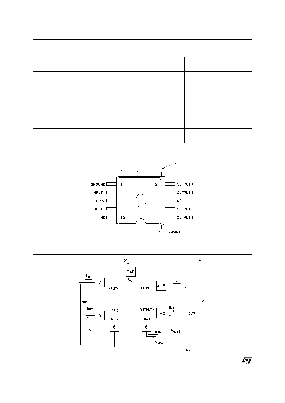
BLOCK DIAG RAM
TYPE V
DSS
R
DS(on
)I
OUT
V
CC
VND10BSP 40 V 0.1 Ω 3.4 A 26 V
■ OUTPUT CURRENT (CONTINUOUS):
14A @ T
c
= 85oC PER CHANNEL
■ 5V LOGIC LEVEL COMPATIBLE INPUT
■ THERMAL SHUT-DOWN
■ UNDER VOLTAG E PROT E CT ION
■ OPEN DRAIN DIAGNOSTIC OUTPUT
■ INDUCTIVE LOAD FAST
DEMAGNETIZATION
■ VERY LOW STAND-BY POWER
DISSIPATION
DESCRIP TION
The VND10BSP is a monolithic device made
using SGS-THOMSON Vertical Intelligent Power
Technology, intended for driving resistive or
inductive loads with one side grounded. This
device has two channels, and a common
diagnostic. Built-in thermal shut-down protects
the chip from over temperature and short circuit.
The status output provides an indication of open
load in on state, open load in off state,
overtemperature conditions and stuc k-on to V
CC
.
1
10
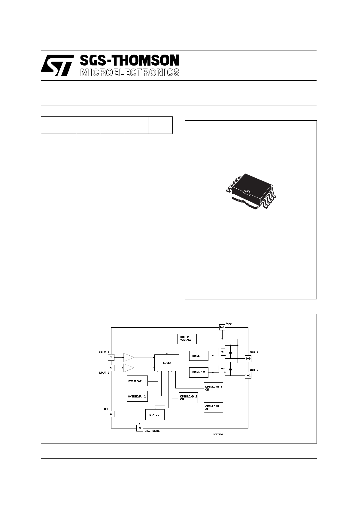
PowerSO-10
1/9
ABSOLUTE MAXIMUM RATING
Symbol Parameter Value Unit
V
(BR)DSS
Drain-Source Breakdown Voltage 40 V
I
OUT
Output Current (cont.) at Tc = 85 oC14A
I
OUT
(RMS) RMS Output Current at Tc = 85 oC and f > 1Hz 14 A
I
R
Reverse Output Current at Tc = 85 oC-14A
I
IN
Input Current ±10 mA
-V
CC
Reverse Supply Voltage -4 V
I
STAT
Status Current ±10 mA
V
ESD
Electrostatic Discharge (1.5 kΩ, 100 pF) 2000 V
P
tot
Power Dissipation at Tc = 25 oC 75 W
T
j
Junction Operating Temperature -40 to 150
o
C
T
stg
Storage Temperature -55 to 150
o
C
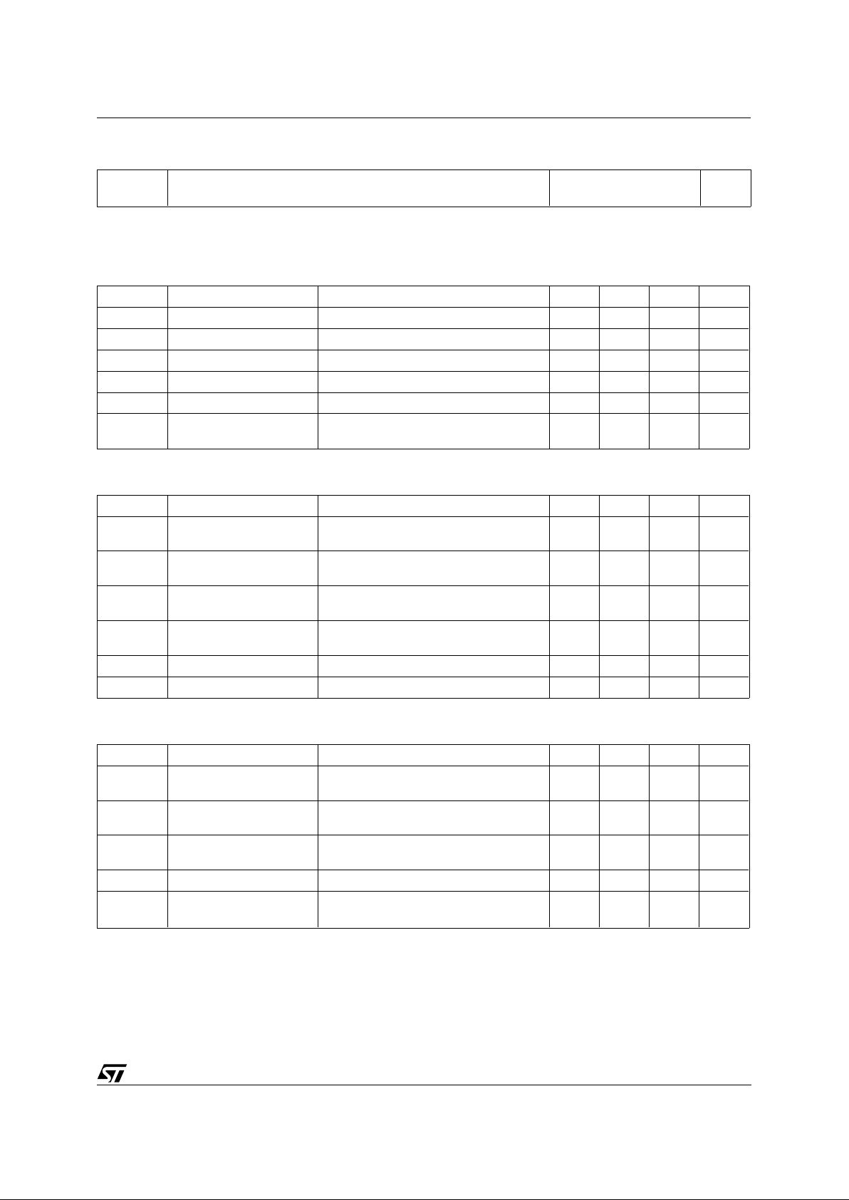
CONNECTION DIAGRAMS
CURRENT AND VOLTAGE CONVENTI ONS
VND10BSP
2/9
THERMAL DATA
R
thj-case
R
thj-amb
Thermal Resistance Junction-case Max
Thermal Resistance Junction-ambient ($) Max
1.65
60
o
C/W
o
C/W
($) When mounted using minimum recommended pad size on FR-4 board
ELECTRICAL CHARACTERISTICS (8 < VCC < 16 V; -40 ≤ Tj ≤ 125 oC unless otherwise specified)
POWER
Symbol Parameter Test Conditions Min. Typ. Max. Unit
V
CC
Supply Voltage 6 13 26 V
In(*) Nominal Current Tc = 85 oC V
DS(on)
≤ 0.5 VCC = 13 V 3.4 5.2 A
R
on
On State Resistance I
OUT
= In VCC = 13 V Tj = 25 oC 0.065 0.1 Ω
I
S
Supply Current Off State Tj = 25 oC VCC = 13 V 35 100 µA
V
DS(MAX)
Maximum Voltage Drop I
OUT
= 7.5 A Tj = 85 oC VCC = 13 V 1.2 2 V
R
i
Output to GND internal
Impedance
Tj = 25 oC 5 10 20 KΩ
SWITCHING
Symbol Parameter Test Conditions Min. Typ. Max. Unit
t
d(on)
(^) Turn-on Delay Time Of
Output Current
R
out
= 2.7 Ω 5 35 200 µs
t
r
(^) Rise Time Of Output
Current
R
out
= 2.7 Ω 28 110 360 µs
t
d(off)
(^) Turn-off Delay Time Of
Output Current
R
out
= 2.7 Ω 10 140 500 µs
t
f
(^) Fall Time Of Output
Current
R
out
= 2.7 Ω 28 75 360 µs
(di/dt)
on
Turn-on Current Slope R
out
= 2.7 Ω 0.003 0.1 A/µs
(di/dt)
off
Turn-off Current Slope R
out
= 2.7 Ω 0.005 0.1 A/µs
LOGIC INP UT
Symbol Parameter Test Conditions Min. Typ. Max. Unit
V
IL
Input Low Level
Voltage
1.5 V
V
IH
Input High Level
Voltage
3.5 (•)V
V
I(hyst.)
Input Hysteresis
Voltage
0.2 0.9 1.5 V
I
IN
Input Current VIN = 5 V Tj = 25 oC 30 100 µA
V
ICL
Input Clamp Voltage IIN = 10 mA
I
IN
= -10 mA
56
-0.7
7V
V
VND10BSP
3/9
 Loading...