

VND10BSP
ISO HIGH SIDE SMART POWER SOLID STATE RELAY
TYPE V
VND1 0B SP 40 V 0. 1 Ω 3.4 A 26 V
■ OUTPUTCURRENT(CONTINUOUS):
14A @ T
■ 5V LOGIC LEVEL COMPATIBLEINPUT
■ THERMALSHUT-DOWN
■ UNDERVOLTAGE PROTECTION
■ OPENDRAIN DIAGNOSTIC OUTPUT
■ INDUCTIVELOAD FAST
=85oC PERCHANNEL
c
DSS
R
DS(on
)I
OUT
V
CC
DEMAGNETIZATION
■ VERY LOW STAND-BY POWER
DISSIPATION
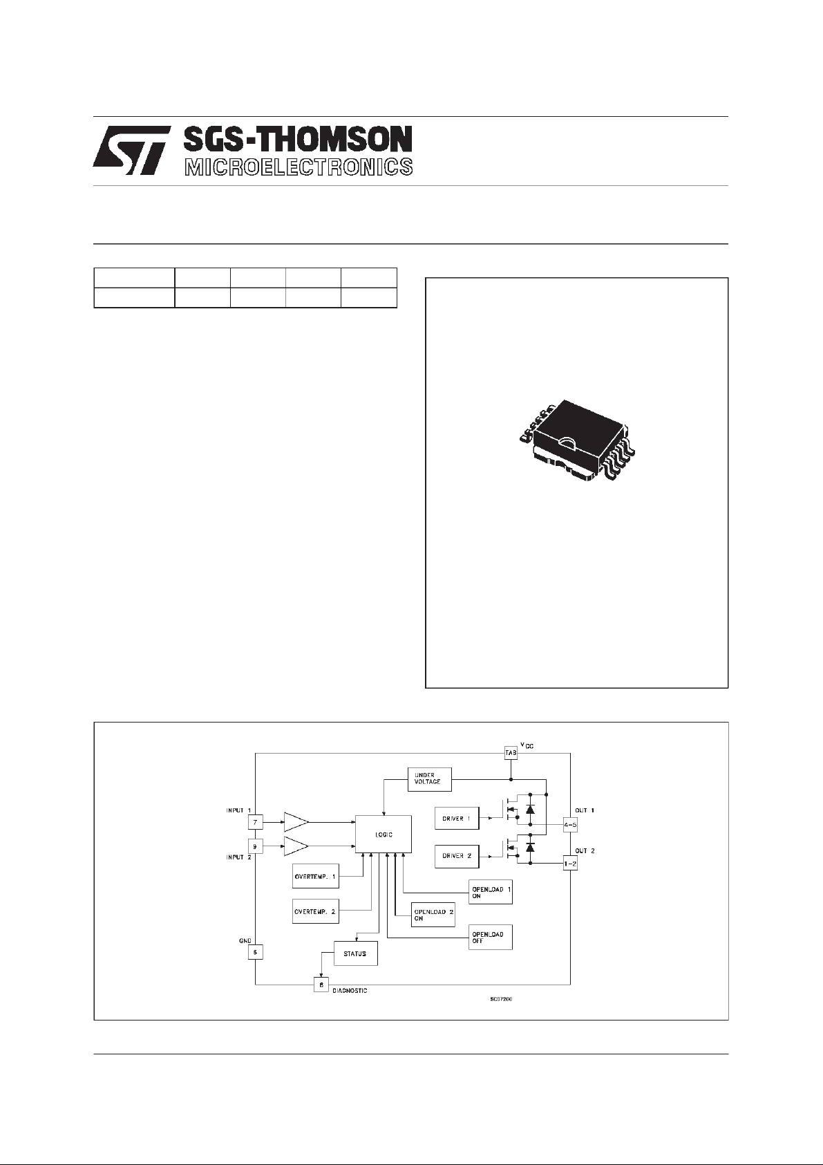
DESCRIPTION
The VND10BSP is a monolithic device made
using SGS-THOMSON Vertical Intelligent Power
Technology, intended for driving resistive or
inductive loads with one side grounded. This
device has two channels, and a common
diagnostic. Built-in thermal shut-down protects
the chip fromover temperatureand shortcircuit.
The statusoutput provides an indicationof open
load in on state, open load in off state,
overtemperatureconditions and stuck-on to V
CC
.
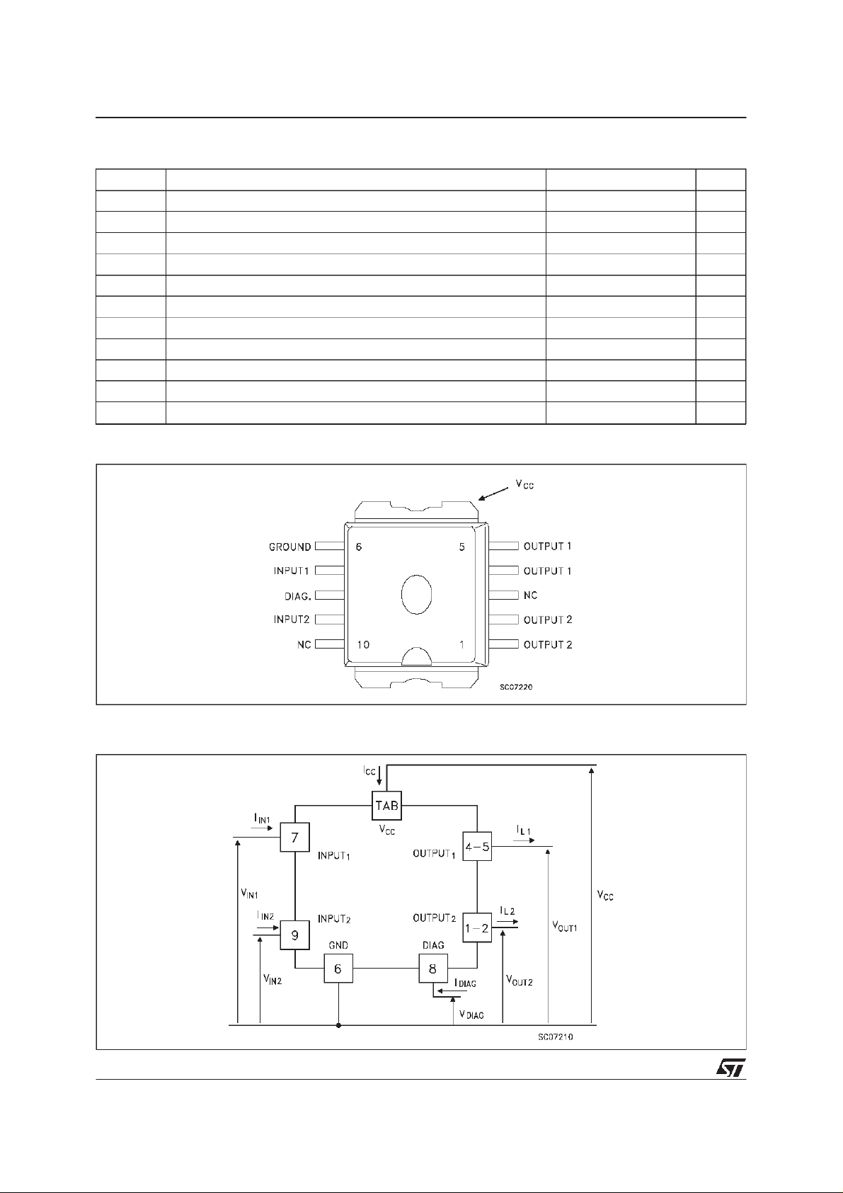
10
1
PowerSO-10
BLOCK DIAGRAM
March 1998
1/9
VND10BSP
ABSOLUTEMAXIMUMRATING
Symb o l Para met er Val u e Uni t
V
(BR)DSS
I
OUT
I
(RMS ) RMS Output Curr ent at Tc=85oC and f > 1Hz 14 A
OUT
I
I
-V
I
STAT
V
ESD
P
T
T
CONNECTION DIAGRAMS
Drain-S o ur ce Br eakdown V olt age 40 V
Out put Current (c on t . ) a t Tc=85oC14A
Revers e Out put Cu rr ent a t Tc=85oC-14A
R
Input Current ±10 mA
IN
Reverse Su pply Voltage -4 V
CC
St at us Current ±10 mA
Elect r o st at ic Disc harge (1.5 kΩ, 100 pF) 2000 V
Power Dissipation at Tc=25oC75W
tot
Junction O per at in g Temperat ure -40 to 150
j
St orage Tem per at ure -55 to 150
stg
o
C
o
C
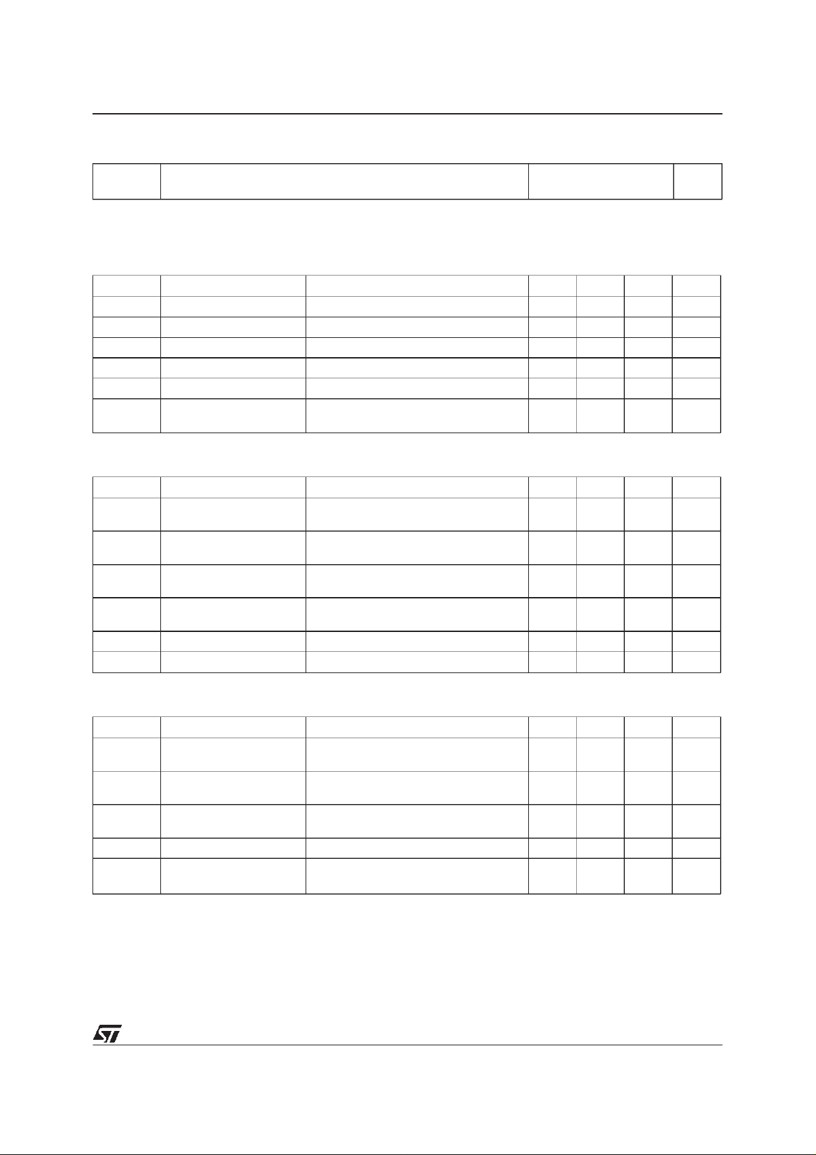
CURRENT AND VOLTAGE CONVENTIONS
2/9
VND10BSP
THERMALDATA
R
thj-case
R
thj-amb
($) When mounted using minimum recommended pad size on FR-4 board
Ther mal Resis t ance Junct io n- case Max
Therm al Res is tance Junction-a mbient ($) Max
1.65
60
ELECTRICAL CHARACTERISTICS (8 < VCC< 16 V; -40 ≤ Tj≤ 125oC unlessotherwise specified)
POWER
Symbol Parameter Test C ondition s Min. Typ. Max. Unit
V
In(*) Nominal Current T
R
I
V
DS(MAX)
R
Supply Voltag e 6 13 26 V
CC
=85oCV
c
On State Resist a nc e I
on
Supply Current Of f St at e Tj=25oCVCC= 13 V 35 100 µA
S
Maximum Voltage Drop I
Out put to GND internal
i
OUT=InVCC
=7.5A Tj=85oCVCC=13V 1.2 2 V
OUT
Tj=25oC51020KΩ
≤ 0.5 VCC=13V 3.4 5.2 A
DS(on)
=13V Tj=25oC 0.065 0.1 Ω
Im pedance
SWITCHING
Symbol Parameter Test C ondition s Min. Typ. Max. Unit
t
(^) Turn- on Delay T im e O f
d(on)
Out put Current
(^) Rise Time O f Output
t
r
Current
(^) Turn- of f Delay Tim e O f
t
d(off)
Out put Current
(^) Fall Time Of Output
t
f
Current
(di/dt)
(di/dt)
Tur n-on Current Slope R
on
Tur n-of f Current S lope R
off
R
=2.7Ω 535200µs
out
R
=2.7Ω 28 110 3 60 µs
out
R
=2.7Ω 10 140 5 00 µs
out
R
=2.7Ω 28 75 360 µs
out
=2.7Ω 0.003 0.1 A / µ s
out
=2.7Ω 0.005 0.1 A / µ s
out
o
o
C/W
C/W
LOGIC INPUT
Symbol Parameter Test C ondition s Min. Typ. Max. Unit
V
V
V
I(hyst.)
I
V
Input Low Level
IL
1.5 V
Volt age
Input High Level
IH
3.5 (•)V
Volt age
Input Hysteresis
0.2 0.9 1.5 V
Volt age
Input Current VIN=5V Tj=25oC30100µA
IN
Input Clamp Volt age IIN=10mA
ICL
=-10mA
I
IN
56
-0.7
7V
V
3/9
 Loading...