

VND10B
DOUBLE CHANNEL
HIGH SIDE SMART POWER SOLID STATE RELAY
PRELIMINARY DATA
TYPE V
VND10B 40 V 0.1 Ω 3.4 A 26 V
■ OUTPUT CURRENT (CONTINUOUS):
DSS
R
DS(on)
In(*) V
CC
14 A @ Tc=85oC PER CHANNEL
■ 5V LOGIC LEVEL COMPATIBLEINPUT
■ THERMAL SHUT-DOWN
■ UNDER VOLTAGE PROTECTION
■ OPEN DRAIN DIAGNOSTIC OUTPUT
■ INDUCTIVELOADFAST DEMAGNETIZATION
■ VERYLOWSTAND-BY POWER DISSIPATION
DESCRIPTION
The VND10B is a monolithic device made using
SGS-THOMSON Vertical Intelligent Power
Technology, intended for driving resistive or
inductive loads with one side grounded. This
device has two channels, and a common
diagnostic. Built-in thermal shut-down protects
the chip from over temperature and short circuit.
The status output provides an indication of open
load in on state, open load in off state,
overtemperature conditions and stuck-on to VCC.
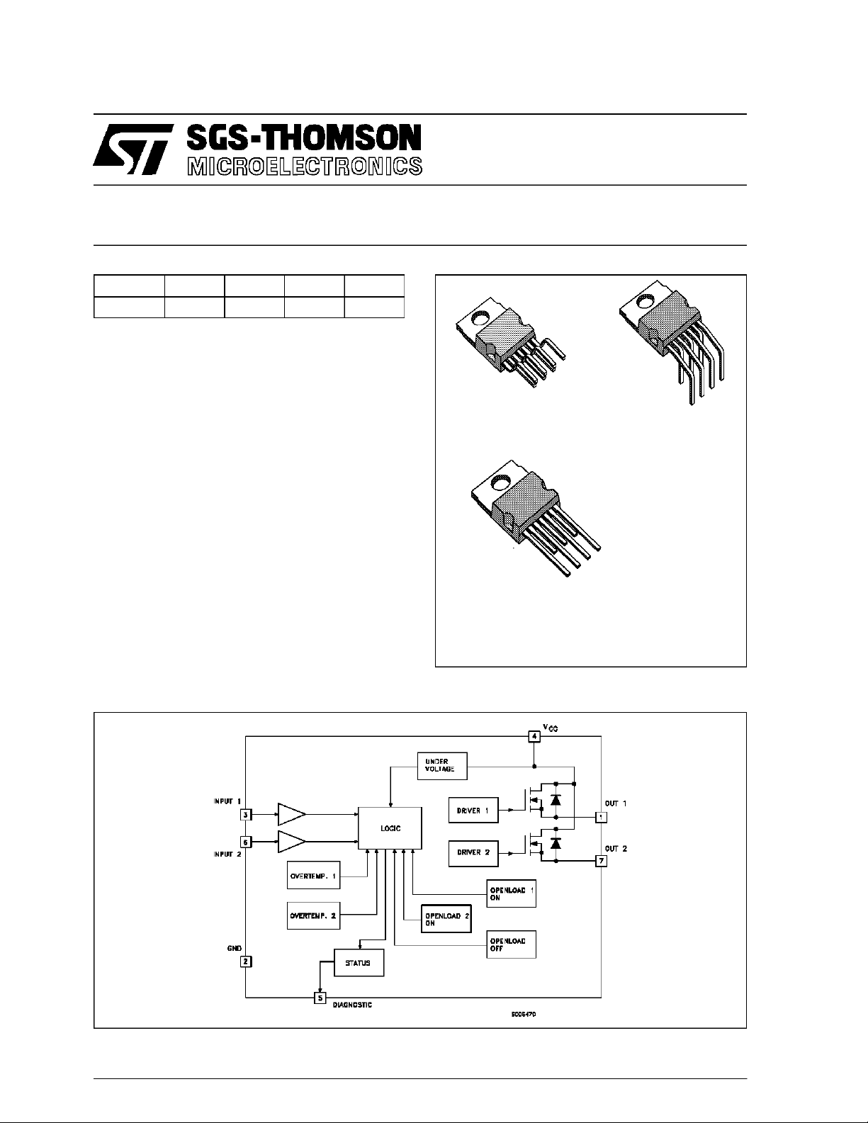
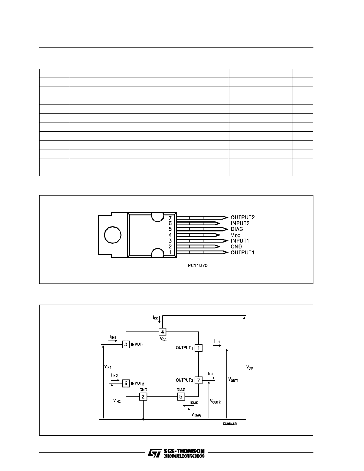
BLOCK DIAGRAM
HEPTAWATT
(vertical)
HEPTAWATT
(horizontal)
HEPTAWATT
(in-line)
ORDER CODES:
HEPTAWATT vertical VND10B
HEPTAWATT horizontal VND10B (011Y)
HEPTAWATT in-line VND10B (012Y)
(*) In= Nominal current accor ding to ISO defini t ion f or high side automoti ve swit ch (see note 1)
September 1994
1/11
VND10B
ABSOLUTE MAXIMUM RATING
Symbol Parameter Value Uni t
V
(BR)DSS
I
OUT
(RMS ) R MS Out put Current at Tc=85oCandf>1Hz 14 A
I
OUT
I
I
-V
I
STAT
V
ESD
P
T
T
CONNECTION DIAGRAM
Drain - So urc e B reakdown Voltage 40 V
Out put Current (cont .) at Tc=85oC14A
Reverse Output Current at Tc=85oC-14A
R
Input Curre nt ±10 mA
IN
Reverse S upply V olt age -4 V
CC
St at us Current ±10 mA
Electrost atic Dischar ge (1.5 kΩ, 100 pF ) 2000 V
Powe r Dissipation at Tc=25oC75W
tot
Junction Operating T emperature -40 to 15 0
j
St or a ge Temper ature -55 to 15 0
stg
o
C
o
C
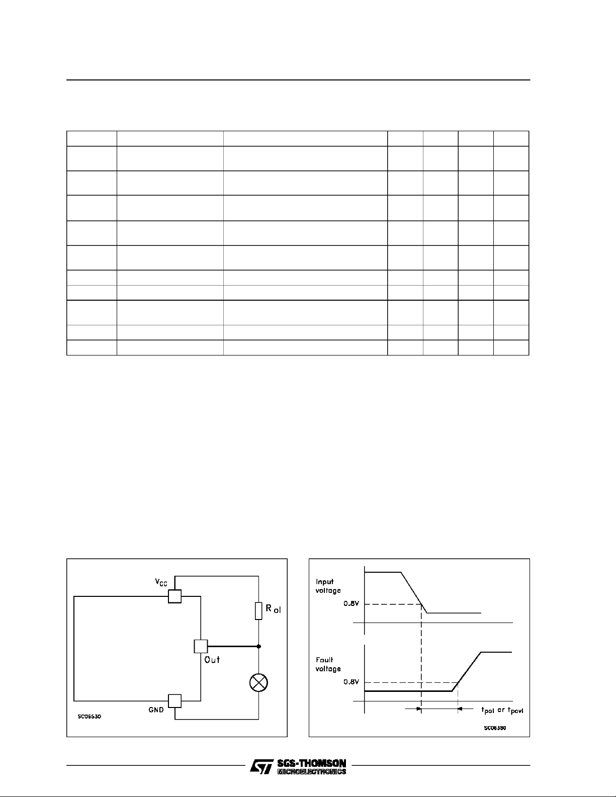
CURRENT AND VOLTAGE CONVENTIONS
2/11
VND10B
THERMAL DATA
R
thj-case
R
thj-amb
Thermal Resistance Junction -c as e Max
Thermal Resistance Junct ion-ambient Max
1.65
60
ELECTRICAL CHARACTERISTICS (8 < VCC< 16 V; -40 ≤ Tj≤ 125oC unless otherwise specified)
POWER
Symbol Parameter Test Condition s Min. Typ. Max. Unit
V
In( *) Nomi na l Curr ent T
R
I
V
DS(MAX)
R
Supply Voltage 6 13 26 V
CC
=85oCV
c
On State Resistance I
on
Supply Cur rent Of f S ta te Tj=25oCVCC= 13 V 35 100 µ A
S
Maximum Voltage D r op I
Out put to GND i n ternal
i
OUT=InVCC
=13A Tj=85oCVCC=13V 1.2 2 V
OUT
Tj=25oC51020KΩ
≤ 0.5 VCC=13V 3.4 5.2 A
DS(on)
=13V Tj=25oC 0.065 0.1 Ω
Im pedance
SWITCHING
Symbol Parameter Test Condition s Min. Typ. Max. Unit
(^) Turn-on Delay Time Of
t
d(on)
Out put Current
t
(^) Rise Time Of Ou t put
r
Current
t
(^) Turn- of f Delay Time Of
d(off)
Out put Current
t
(^) Fall Time Of Output
f
Current
(di/dt)
(di/dt)
Turn-on C urrent S lope R
on
Turn-off Current Slope R
off
R
=2.7Ω 5 35 200 µs
out
R
=2.7Ω 28 110 360 µs
out
R
=2.7Ω 10 140 500 µs
out
R
=2.7Ω 28 75 360 µs
out
=2.7Ω 0.003 0.1 A/µs
out
=2.7Ω 0.005 0.1 A/µs
out
o
o
C/W
C/W
LOGIC INPUT
Symbol Parameter Test Condition s Min. Typ. Max. Unit
V
IL
V
IH
V
I(hyst.)
I
IN
V
ICL
Input Low Level
Volt age
Input High Level
3.5 ( •)V
Volt age
Input Hys teresis
0.2 0.9 1.5 V
Volt age
Input Curre nt VIN=5V Tj=25oC 30 100 µ A
Input Clamp V olt a ge IIN=10mA
IIN=-10mA
56
-0.7
1.5 V
7V
V
3/11
VND10B
ELECTRICAL CHARACTERISTICS (continued)
PROTECTION AND DIAGNOSTICS
Symbol Parameter Test Condition s Min. Typ. Max. Unit
V
STAT
St at us Volta ge Output
Low
V
USD
Under Volta ge Shut
Down
V
SCL
T
TSD
St at us Clamp Voltage I
Thermal Shut-dow n
Tem perature
T
SD( hyst.)
Thermal Shut-dow n
Hysteresis
T
V
I
OL
Reset Tem perature 125
R
Open Voltage Level Off-State (note 2) 2.5 4 5 V
OL
Open Load Cu r rent
Level
t
povl
t
pol
(*) In= Nominal current accor ding to ISO defini t ion f or high side automoti ve swit ch (see note 1)
(^) See swit c hing ti m e w av eform
(•)TheVIHis internal ly clamped at 6V about. It is possible t o connect this pin to an higher voltage via an external r es istor
cal culated to not exceed 10 mA at the i nput pin.
note 1: The Nominal Current is t he current at Tc=85oC for battery voltage of 13V which produces a voltage drop of 0.5 V
note 2: I
note 3: t
St at us Delay (note 3) 5 10 µs
St at us Delay (note 3) 50 500 2500 µs
=(VCC-VOL)/R
OL(off)
: ISO definition
povltpol
OL
I
=1.6mA 0.4 V
STAT
3.5 4.5 6 V
STAT
I
STAT
=10mA
=-10mA
56
-0.7
7V
140 160 180
50
On-State 0.6 0.9 1.4 A
V
o
C
o
C
o
C
Note 2 Relevant Figure Note 3 Relevant Figure
4/11

Switching Time Waveforms
VND10B
FUNCTIONAL DESCRIPTION
The device has a common diagnostic output for
both channels which indicates open load in
on-state, open load in off-state, over temperature
conditions and stuck-on to VCC.
From the falling edge of the input signal, the
status output, initially low to signal a fault
condition (overtemperature or open load
on-state), will go back to a high state with a
different delay in case of overtemperature (tpovl)
and in case of open open load (tpol) respectively.
This feature allows to discriminate the nature of
the detected fault. To protect the device against
short circuit and over current condition, the
thermal protection turns the integrated Power
MOS off at a minimum junction temperature of
140oC. When this temperature returns to 125oC
the switch is automatically turned on again. In
short circuit the protection reacts with virtually no
delay, the sensor (one for each channel) being
located inside each of the two Power MOS areas.
This positioning allows the device to operate with
one channel in automatic thermal cycling and the
other one on a normal load. An internal function
of the devices ensures the fast demagnetization
of inductive loads with a typical voltage (V
demag
of -18V. This function allows to greatly reduces
the power dissipation according to the formula:
P
dem
=0.5•L
load
• (I
load
)2• [(VCC+V
demag
)/V
demag
]• f
where f = switching frequency and
V
= demagnetization voltage.
demag
The maximum inductance which causes the chip
temperature to reach the shut-down temperature
in a specified thermal environment is afunction of
the load current for a fixed VCC, Vdemag and f
according to the above formula. In this device if
the GND pin is disconnected, with VCCnot
exceeding 16V, both channel will switch off.
PROTECTING THE DEVICE AGAINST
REVERSE BATTERY
The simplest way to protect the device against a
continuous reverse battery voltage (-26V) is to
insert a Schottky diode between pin 2 (GND) and
ground, as shown in the typical application circuit
(fig. 2).
The consequences of the voltage drop across
this diode are as follows:
– If the input is pulled to power GND, a negative
voltage of -Vfis seen by the device. (Vil, Vih
thresholds and Vstat are increased by Vf with
respect to power GND).
– The undervoltage shutdown level is increa-
sed by Vf.
If there is no need for the control unit to handle
external analog signals referred to the power
GND, the best approach is to connect the
)
reference potential of the control unit to the
device ground (see application circuit in fig. 3),
which becomes the common signal GND for the
whole control board avoiding shift of Vih,Viland
V
. This solution allows the use of a standard
stat
diode.
5/11

VND10B
TRUTH TABLE
INP UT 1 INPUT 2 OUTPUT 1 OUTPUT 2 DIAGNOS T I C
Normal O per at ion L
H
L
H
Under-v oltage X X L L H
Ther mal Shutd ow n
Open L oad
Output Shorted to V
CC
Channel 1
Channel 2
Channel 1
Channel 2
Channel 1
Channel 2
HXLX L
XHXL L
H
L
X
L
H
L
X
L
Figure 1: Waveforms
L
H
H
L
X
L
H
L
X
L
H
L
L
H
L
H
H
L
X
L
H
H
X
L
L
H
H
L
X
L
H
L
X
L
H
H
H
H
H
H
L
L(**)
L
L(**)
L
L
L
L
6/11

Figure 2: Typical ApplicationCircuit With A Schottky Diode For Reverse Supply Protection
VND10B
Figure 3: Typical ApplicationCircuit With Separate Signal Ground
7/11

VND10B
Heptawatt (vertical) MECHANICAL DATA
DIM.
A 4.8 0.189
C 1.37 0.054
D 2.4 2.8 0.094 0.110
D1 1.2 1.35 0.047 0.053
E 0.35 0.55 0.014 0.022
F 0.6 0.8 0.024 0.031
F1 0.9 0.035
G 2.41 2.54 2.67 0.095 0.100 0.105
G1 4.91 5.08 5.21 0.193 0.200 0.205
G2 7.49 7.62 7.8 0.295 0.300 0.307
H2 10.4 0.409
H3 10.05 10.4 0.396 0.409
L 16.97 0.668
L1 14.92 0.587
L2 21.54 0.848
L3 22.62 0.891
L5 2.6 3 0.102 0.118
L6 15.1 15.8 0.594 0.622
L7 6 6.6 0.236 0.260
M 2.8 0.110
M1 5.08 0.200
MIN. TYP. MAX. MIN. TYP. MAX.
mm inch
8/11
P023A

Heptawatt (horizontal) MECHANICAL DATA
VND10B
DIM.
A 4.8 0.189
C 1.37 0.054
D 2.4 2.8 0.094 0.110
D1 1.2 1.35 0.047 0.053
E 0.35 0.55 0.014 0.022
F 0.6 0.8 0.024 0.031
F1 0.9 0.035
G 2.41 2.54 2.67 0.095 0.100 0.105
G1 4.91 5.08 5.21 0.193 0.200 0.205
G2 7.49 7.62 7.8 0.295 0.300 0.307
H2 10.4 0.409
H3 10.05 10.4 0.396 0.409
L 14.2 0.559
L1 4.4 0.173
L2 15.8 0.622
L3 5.1 0.201
L5 2.6 3 0.102 0.118
L6 15.1 15.8 0.594 0.622
L7 6 6.6 0.236 0.260
L9 4.44 0.175
Dia 3.65 3.85 0.144 0.152
MIN. TYP. MAX. MIN. TYP. MAX.
mm inch
P023B
9/11

VND10B
Heptawatt (In-Line) MECHANICAL DATA
DIM.
MIN. TYP. MAX. MIN. TYP. MAX.
A 4.8 0.189
C 1.37 0.054
D 2.4 2.8 0.094 0.110
D1 1.2 1.35 0.047 0.053
E 0.35 0.55 0.014 0.022
F 0.6 0.8 0.024 0.031
F1 0.9 0.035
G 2.41 2.54 2.67 0.095 0.100 0.105
G1 4.91 5.08 5.21 0.193 0.200 0.205
G2 7.49 7.62 7.8 0.295 0.300 0.307
H2 10.4 0.409
H3 10.05 10.4 0.396 0.409
L2 22.4 22.9 0.882 0.902
L3 25.4 26 1.000 1.024
L5 2.6 3 0.102 0.118
L6 15.1 15.8 0.594 0.622
L7 6 6.6 0.236 0.260
Dia 3.65 3.85 0.144 0.152
mm inch
10/11
P023C

VND10B
Information furnished is believed to beaccurate and reliable. However, SGS-THOMSON Microelectronics assumes no responsability for the
consequences of use of such informationnor for any infringementof patents orother rights of third parties which may results from its use. No
license isgranted byimplication orotherwise underany patentor patentrights ofSGS-THOMSON Microelectronics.Specificationsmentioned
in this publicationare subject to changewithout notice. This publication supersedesand replaces all informationpreviously supplied.
SGS-THOMSON Microelectronicsproducts arenot authorizedfor useas criticalcomponentsin life supportdevices orsystemswithout express
written approvalof SGS-THOMSON Microelectonics.
1994 SGS-THOMSON Microelectronics- All Rights Reserved
Australia - Brazil- France- Germany- Hong Kong -Italy -Japan - Korea - Malaysia -Malta - Morocco - The Netherlands -
Singapore -Spain - Sweden - Switzerland -Taiwan - Thailand - UnitedKingdom - U.S.A
SGS-THOMSON MicroelectronicsGROUP OF COMPANIES
11/11
 Loading...