®
VN920DSP
HIGH SIDE DRIVER
TYPE R
DS(on)
I
OUT
V
CC
VN920DSP 16 mΩ 25 A 36 V
■ CMOS COMPATIBLE INPUT
■ ON STATE OPEN LOAD DETECTION
■ OFF STATE OPEN LOAD DETECTION
■ SHORTED LOAD PROTECTION
■ UNDERVOLTAGE AND OVERVOLTAGE
SHUTDOWN
■ PROTECTION AGAINST LOSS OF GROUND
■ VERY LOW STAND-BY CURRENT
■ REVERSE BATTERY PROTECTION (*)
DESCRIPTION
The VN920DSP is a monolithic device ma de by
using STMicroelectronics VIPower M0-3
Technology, i ntended for dr iving any kind o f load
with one side connected to ground.
Active VCC pin voltage clamp prote cts the device
against low energy spikes (see ISO7637 transient
compatibility table). Active current limitation
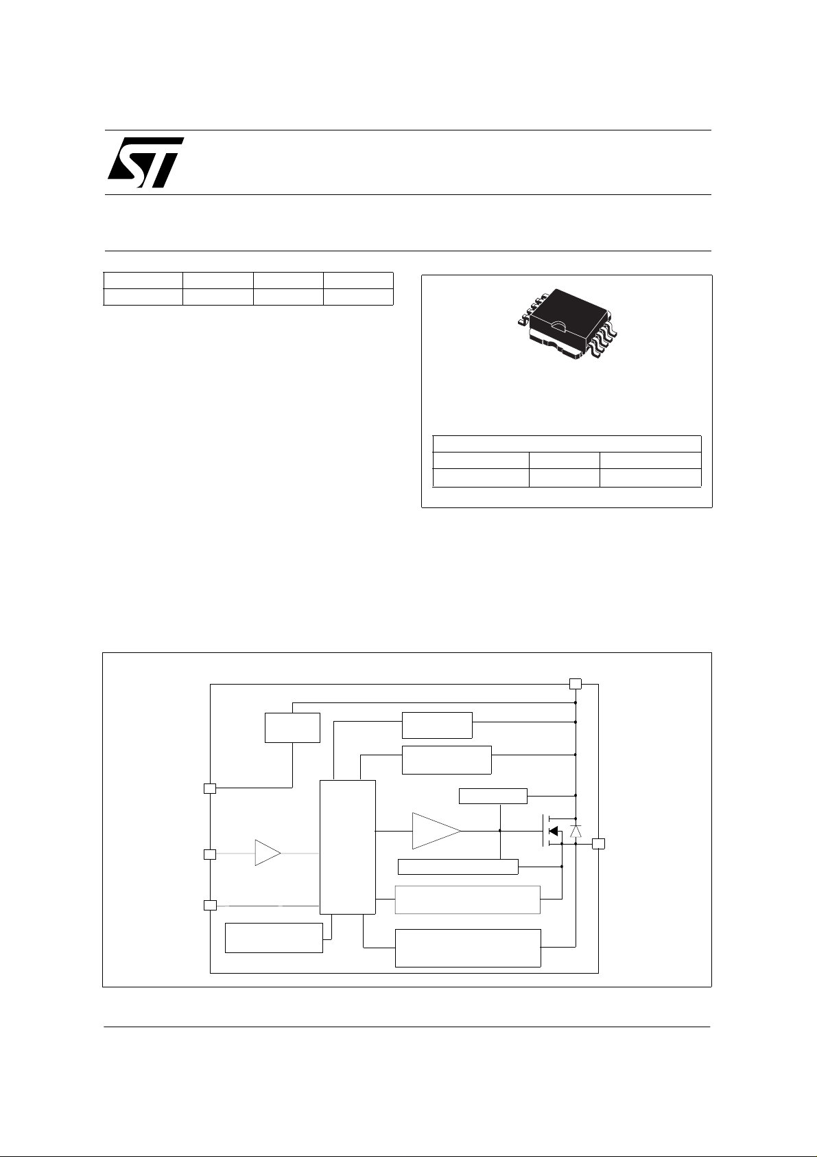
BLOCK DIAGRAM
10
1
PowerSO-10™
ORDER CODES
PACKAGE TUBE T&R
PowerSO-10™
VN920DSP VN920DSP13TR
combined with thermal shutdown and automatic
restart protect the device against overload.
The device detects open load condition both is on
and off state. Output shorted to VCC is detected in
the off state. Device automatically turns off in case
of ground pin disconnection.
V
CC
OVERVOLTAGE
DETECTION
UNDERVOLTAGE
DETECTION
Power CLAMP
DRIVER
CURRENT LIMITER
ON STATE OPENLOAD
DETECTION
OFF STA TE OPENLOAD
AND OUTPUT SHORTED TO V
DETECTION
OUTPUT
CC
GND
INPUT
STATUS
OVERTEMPERATURE
DETECTION
(*) See application schematic at page 8
V
CC
CLAMP
LOGIC
October 20 02 1/17
VN920DSP
ABSOLUTE MAXIMUM RATI NG
Symbol Parameter Value Unit
DC Supply Vol tage 41 V
V
CC
- V
- I
- I
I
V
E
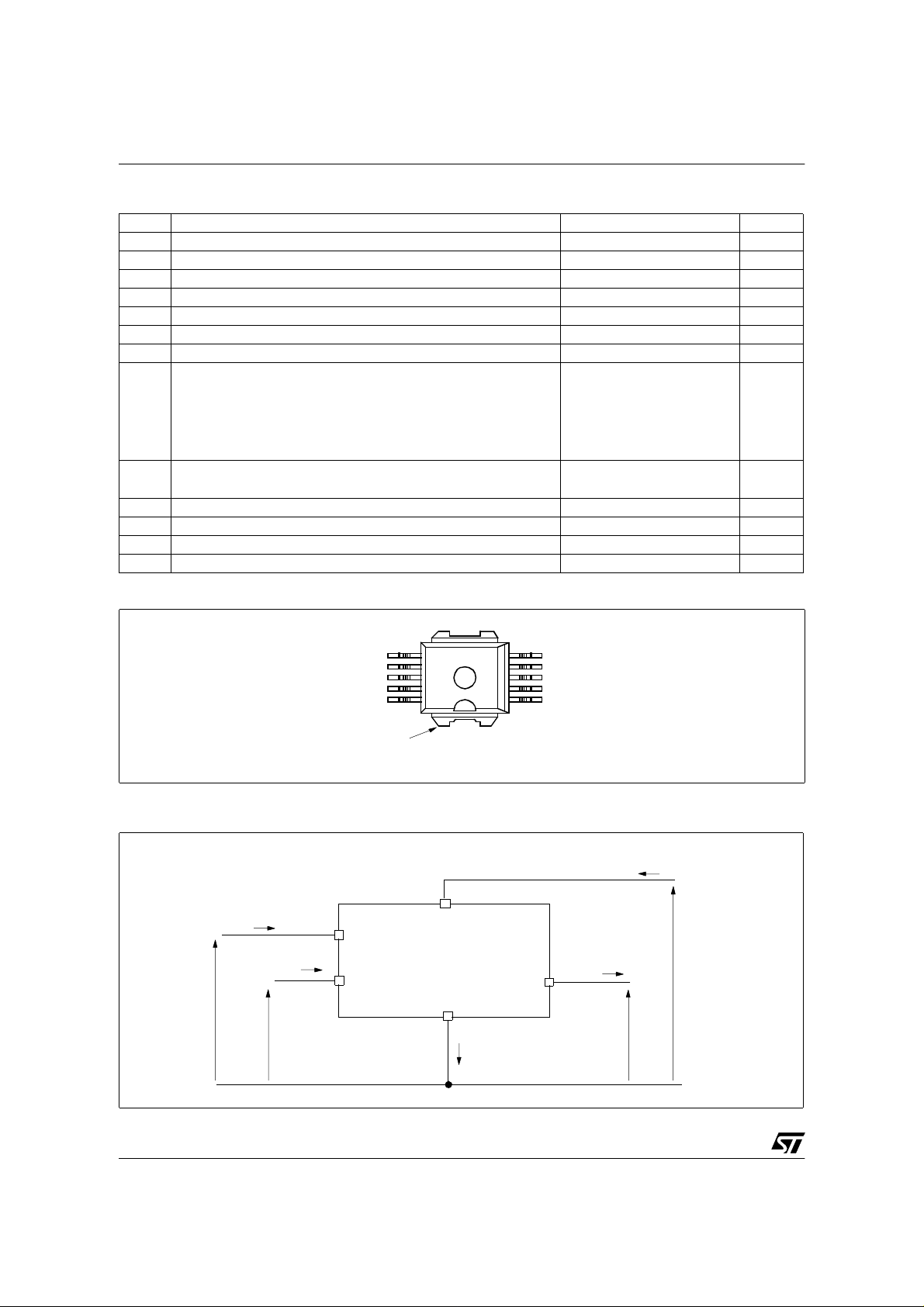
CONNECTION DIAGRAM (TOP VIEW)
Reverse DC Supply Voltage - 0.3 V
CC
DC Reverse Ground Pin Current - 200 mA
GND
DC Output Current Internally Limited A
I
OUT
Reverse DC Ou tput Current - 25 A
OUT
DC Input Curre nt +/- 10 mA
I
IN
DC Status Curr ent +/- 10 mA
STAT
Electro static Discharge (Human Body Model: R=1. 5KΩ; C=100pF)
- INPUT
- CURRENT SENSE
ESD
- OUTPUT
- V
CC
Maximum Switching Energy
MAX
(L=0.25mH; R
Power Diss ip ation TC=25°C 96.1 W
P
tot
Junction Operating Temperature Internally Limited °C
T
j
Case Oper ating Temperature - 40 to 150 °C
T
c
Storage Temperature - 55 to 150 °C
T
stg
=0Ω; V
L
=13.5V; T
bat
=150ºC; IL=45A)
jstart
4000
4000
5000
5000
362 mJ
V
V
V
V
GROUND
INPUT
STATUS
N.C.
N.C.
V
CURRENT AND VOLTAGE CONVENTIONS
I
IN
INPUT
I
STAT
STATUS
V
IN
V
STAT
6
7
8
9
10
11
CC
PowerSO-10™
V
CC
OUTPUT
GND
I
GND
5
4
3
2
1
OUTPUT
OUTPUT
N.C.
OUTPUT
OUTPUT
I
OUT
V
OUT
I
S
V
CC
2/17
1
VN920DSP
THERMAL DATA
Symbol Parameter Value Unit
CC
OV
ON
S
Thermal R esistance Junct ion-case Max 1.3 °C/W
Thermal Resistanc e Junctio n-ambient Max 51.3 (*) °C/W
Operating Supply Voltage 5.5 13 36 V
Undervolt age Shut-down 3 4 5.5 V
Undervolt age Shut-down
hysteresis
0.5 V
Overvolt age Shut-down 36 V
=10A; Tj=25°C
I
OUT
On State Resistance
I
=10A
OUT
I
=3A; VCC=6V
OUT
Off Stat e; V
Supply Current
Off Stat e; V
Tj=25°C
On State; V
Off State Output Current VIN=V
OUT
Off State Output Current VIN=0V; V
Off State Output Current VIN=V
Off State Output Current VIN=V
OUT
OUT
=13V; VIN=V
CC
=13V; VIN=V
CC
OUT
OUT
=0V
=0V;
10
10
=13V; VIN=5V; I
CC
OUT
=0A
=0V 0 50 µA
=3.5V -75 0 µA
OUT
=0V; VCC=13V; Tj =125°C 5 µ A
=0V; VCC=13V; Tj =25°C 3 µ A
16
30
50
25
20
5
R
thj-case
R
thj-amb
(*) When mounted on a standard single-sided FR-4 board with 0.5cm2 of Cu (at leas t 35µ m t hick) .
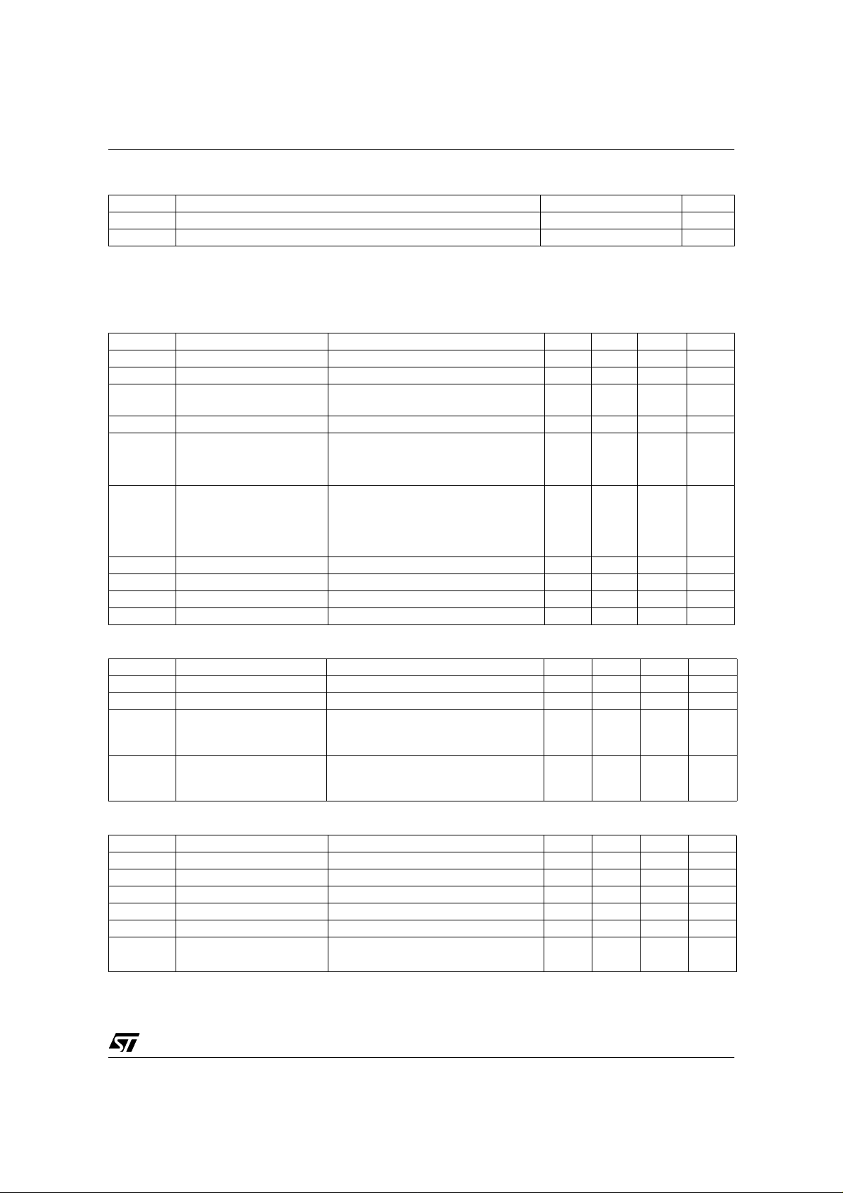
ELECTRICAL CHARACTERISTICS (8V<VCC<36V; -40°C<Tj<150°C unless otherwise specified)
POWER
Symbol Parameter Test Conditions Min Typ Max Unit
V
V
USD
V
USDhyst
V
R
I
I
L(off1)
I
L(off2)
I
L(off3)
I
L(off4)
mΩ
mΩ
mΩ
µA
µA
mA
SWITCHING (VCC=13V)
Symbol Parameter Test Conditions Min Typ Max Unit
(on)
(off)
Turn-on Delay Time RL=1.3Ω 50 µs
Turn-off Delay Time RL=1.3Ω 50 µs
/
Turn-on Voltage Slope RL=1.3Ω
See
relative
diagram
/
Turn-off Voltage Slope RL=1.3Ω
See
relative
diagram
dV
dV
t
d(on)
t
d(off)
dt
dt
OUT
OUT
INPUT PIN
Symbol Parameter Test Conditions Min Typ Max Unit
IL
IL
IH
IH
ICL
Input Low Level 1.25 V
Low Level Input Current VIN=1.25V 1 µA
Input High Level 3.25 V
High Level Input Current VIN=3.25V 10 µA
Input Hyst eresis Vo ltage 0.5 V
I
Input Clamp Voltage
IN
I
IN
=1mA
=-1mA
66.8
-0.7
8V
V
I(hyst)
V
V
I
V
I
V/µs
V/µs
V
3/17
1

VN920DSP
ELECTRICAL CHARACTERISTICS (continued)
STATUS PIN
Symbol Parameter Test Conditions Min Typ Max Unit
V
STAT
I
LSTAT
C
STAT
V
SCL
Status Low Output Voltage I
Status Leakage Current Normal Operation V
Status Pin Input
Capacitance
Status Clamp Voltage
PROTECTIONS
Symbol Parameter Test Conditions Min Typ Max Unit
T
T
t
V
demag
TSD
T
hyst
SDL
I
lim
Shut-down Temperature 150 175 200 °C
Reset Temp erature 135 °C
R
Ther ma l Hy steresi s 7 15 °C
Statu s delay in overload
condition
Current limitation
Turn-off Output Clamp
Voltage
=1.6mA 0.5 V
STAT
Normal Operation V
=1mA
I
STAT
I
=-1mA
STAT
T
j>TTSD
=5V 10 µA
STAT
=5V 100 pF
STAT
66.8
-0.7
20 µs
30 45 75
5.5V<V
I
OUT
CC
<36V
75
=2A; VIN=0V; L= 6m H VCC-41 VCC-48 VCC-55 V
8V
V
A
A
OPENLOAD DETECTION
Symbol Parameter Test Conditions Min Typ Max Unit
OL
Openload ON State
Detectio n Threshol d
Openload ON State
Detection Delay
Openload OFF State
Voltage Det ection
Threshold
Openl o ad Detection De lay
at Turn Off
V
> V
OUT
t
DOL(off)
=5V 300 500 700 mA
V
IN
=0A 200 µs
I
OUT
V
=0V 1.5 2.5 3.5 V
IN
1000 µs
OVERTEMP STATUS TIMING
I
< I
OUT
t
DOL(on)
OL
V
V
IN
STAT
t
SDL
Tj > T
TSD
t
SDL
OL
I
OL
t
DOL(on)
V
t
DOL(off)
OPEN LOAD STATUS TIMING (with external pull-up)
V
IN
V
STAT
4/17
2
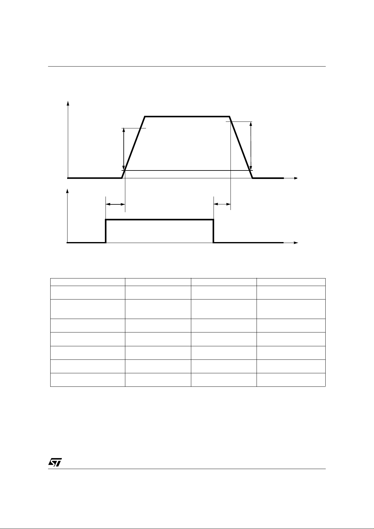
Switching time Waveforms
V
OUT
dV
/dt
OUT
(on)
V
IN
t
d(on)
80%
10%
t
d(off)
90%
dV
OUT
/dt
VN920DSP
(off)
t
t
TRUTH TABLE
CONDITIONS INPUT OUTPUT STATUS
Normal Operation
Cur rent Limitation
Overtemperature
Undervoltage
Overvoltage
Output Voltage > V
Output Current < I
OL
OL
L
H
L
H
H
L
H
L
H
L
H
L
H
L
H
L
H
L
X
X
< T
(T
j
> T
(T
j
L
L
L
L
L
L
H
H
L
H
TSD
TSD
H
H
H
) H
) L
H
L
X
X
H
H
L
H
H
L
5/17
VN920DSP
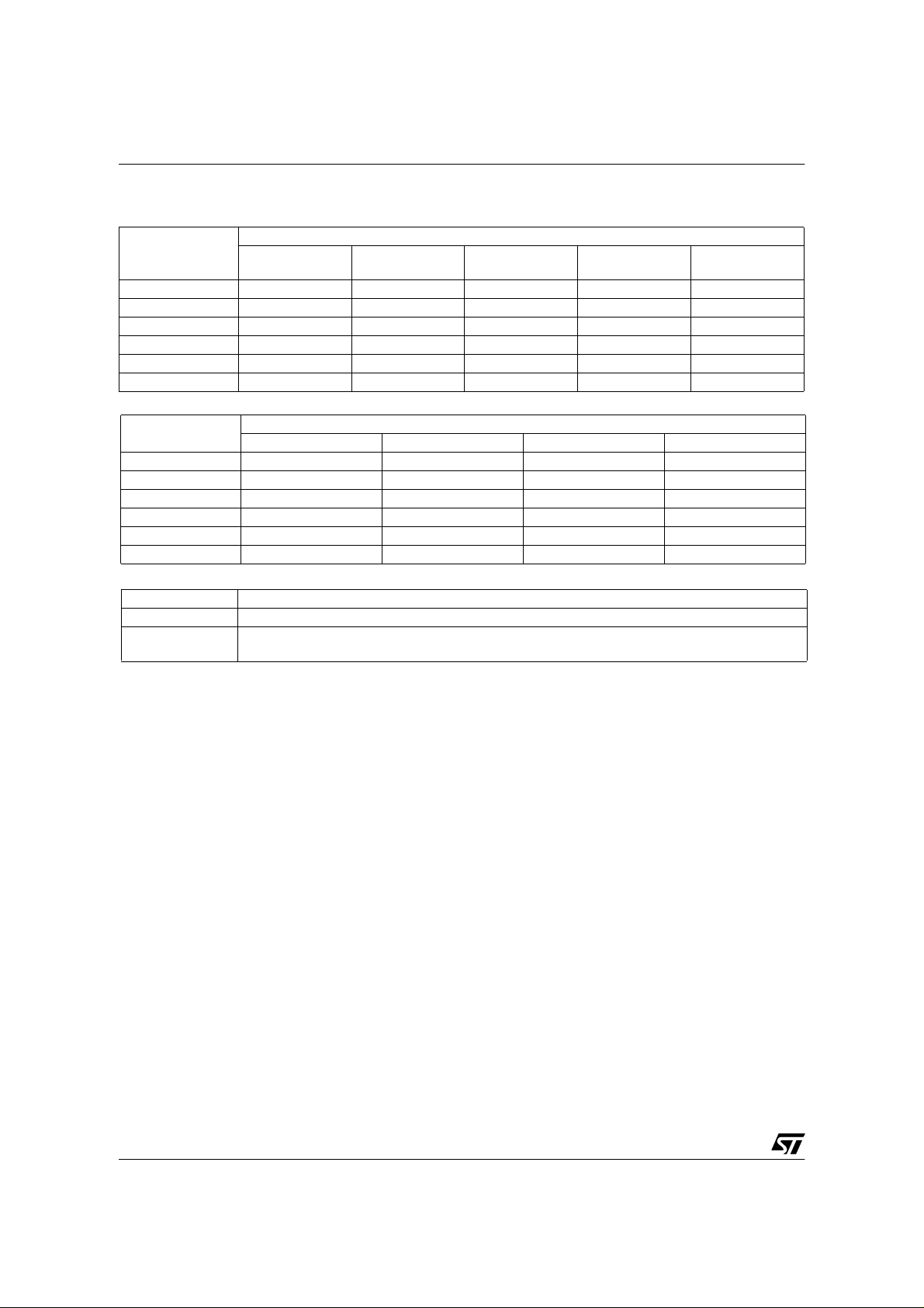
ELECTRICAL TRANSIENT REQUIREMENTS ON VCC PIN
ISO T/R 7637/1
Test Pulse
1 -25 V -50 V -75 V -100 V 2 m s 10 Ω
2 +25 V +50 V +75 V +100 V 0.2 ms 10 Ω
3a -25 V -50 V - 100 V -150 V 0.1 µs 50 Ω
3b +25 V +50 V +75 V +100 V 0.1 µs 50 Ω
4 -4 V -5 V -6 V -7 V 100 ms, 0.01
5 +26.5 V +46.5 V +66.5 V +86.5 V 400 ms, 2
ISO T/R 7637/1
Test P ulse
1CCCC
2CCCC
3aCCCC
3bCCCC
4CCCC
5CEEE
CLASS CONTENTS
C All functions of the devi ce are performed as designed after exposure to disturbance.
E One or more fu nctions of the device is not performed as designed after exposure to disturbance
and canno t be retur ned to proper opera tion without repla cing the device.
I II III IV Delays and
IIIIIIIV
TEST LEVELS
TEST LEVEL S RESULTS
Impedance
Ω
Ω
6/17
 Loading...