

®
VN920D-B5
/ VN920DSO
HIGH SIDE DRIVER
TYPE R
VN920D-B5
VN920DSO
■ CMOS COMPATIBLE INPUT
■ ON STATE OPEN LOAD DETECTION
■ OFF STATE OPEN LOAD DETECTION
■ SHORTED LOAD PROTECTION
■ UNDERVOLTAGE AND OVERVOLTAGE
DS(on)
18 mΩ 30 A 36 V
I
OUT
V
CC
SHUTDOWN
■ PROTECTION AGAINST LOSS OF GROUND
■ VERY LOW STAND-BY CURRENT
■ REVERSE BATTERY PROTECTION (*)
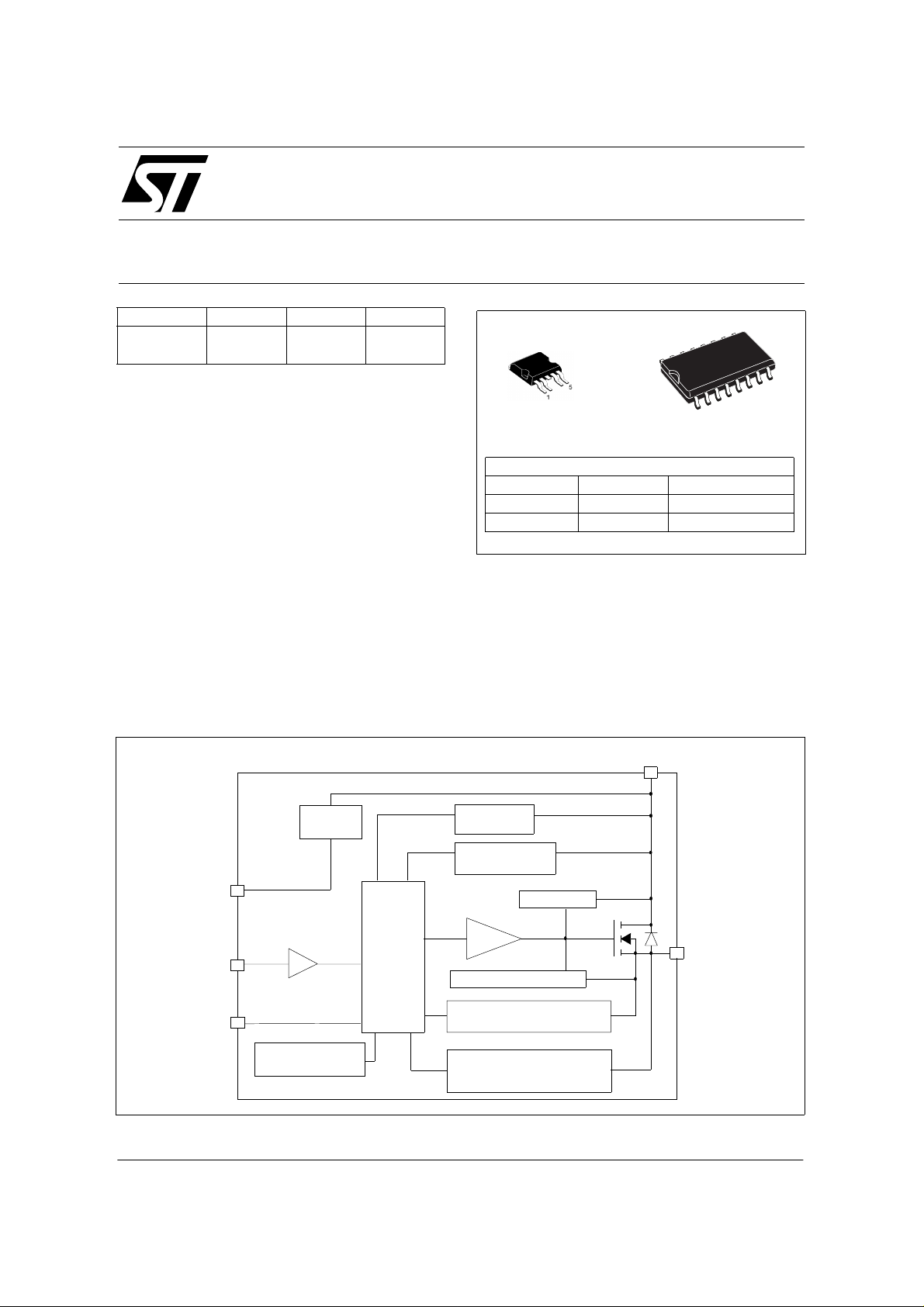
DESCRIPTION
The VN920D-B5, VN920DSO are monolithic
devices made by using STMicroelectronics
VIPower M0-3 Technology, intended for driving
any kind of load with one side connected to
ground. Active VCC pin voltage clamp protects the
device against low ene rgy spikes (see ISO7637
BLOCK DIAGRAM
P2PAK
SO-16L
ORDER CODES
PACKAGE TUBE T&R
SO-16L VN920DSO VN920DSO13TR
P2PAK VN920D-B5 VN920D-B513TR
transient compatibility table). Active current
limitation combined with thermal shutdown and
automatic restart protect the device against
overload.
The device detects open load condition both is on
and off state. Output shorted to VCC is detected in
the off state. Device automatically turns off in case
of ground pin disconnection.
V
CC
OVERVOLTAGE
DETECTION
UNDERVOLTAGE
DETECTION
Power CLAMP
DRIVER
CURRENT LIMITER
ON STATE OPENLOAD
DETECTION
OFF STA TE OPENLOAD
AND OUTPUT SHORTED TO V
DETECTION
OUTPUT
CC
GND
INPUT
STATUS
OVERTEMPERATURE
DETECTION
(*) See application schematic at page 8
V
CC
CLAMP
LOGIC
Janua ry 20 03 1/22
VN920D-B5 / VN920DSO
ABSOLUTE MAXIMUM RATI NG
Symbol Parameter
DC Supply Vol tage 41 V
V
CC
- V
- I
- I
I
V
E
Reverse DC Supply Voltage - 0.3 V
CC
DC Reverse Ground Pin Current - 200 mA
GND
DC Output Current Internally Limited A
I
OUT
Reverse DC Ou tput Current - 25 A
OUT
DC Input Current +/- 10 mA
I
IN
DC Status Current +/- 10 mA
STAT
Electro static Discharge (Hu m an Body Mode l: R=1.5KΩ; C=100pF)
- INPUT
- CURRENT SENSE
ESD
- OUTPUT
- V
CC
Maximum Switching Energy
MAX
(L=0.25mH; R
Power Diss ip ation TC=25°C 96.1 8.3 W
P
tot
Junction Operating Temperature Internally Limited °C
T
j
Case Oper ating Temperature - 40 to 150 °C
T
c
Storage Temperature - 55 to 150 °C
T
stg
=0Ω; V
L
=13.5V; T
bat
jstart
=150ºC; IL=45A)
Value
2
P
PAK SO-16L
4000
4000
5000
5000
364 352 mJ
Unit
V
V
V
V
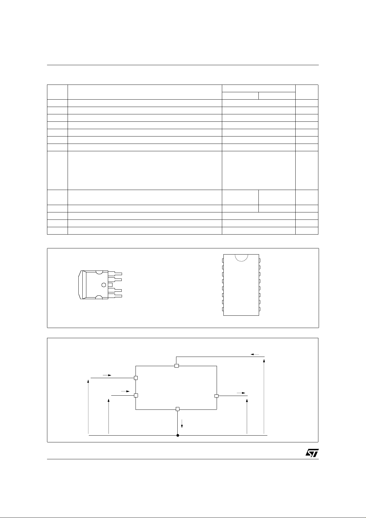
CONNECTION DIAGRAM (TOP VIEW)
5
OUTPUT
4
STATUS
3
V
CC
2
INPUT
1
GND
P2PAK
CURRENT AND VOLTAGE CONVENTIONS
I
IN
INPUT
I
STAT
STATUS
V
IN
V
STAT
V
CC
GND
V
N.C.
GND
INPUT
STA T US
N.C.
N.C.
V
OUTPUT
I
GND
CC
CC
1
8
V
16
9
CC
OUTPUT
OUTPUT
OUTPUT
OUTPUT
OUTPUT
OUTPUT
V
CC
SO-16L
I
S
I
OUT
V
CC
V
OUT
2/22
VN920D-B5 / VN920DSO
THERMAL DATA
Symbol Parameter
R
thj-case
R
thj-lead
R
thj-amb
(*) When mounted on a standard single-sided FR-4 board with 0.5cm2 of Cu (at leas t 35µ m t hick) .
(**) When mounted on FR4 printed circuit board with 0.5cm
Thermal Resistanc e Junctio n-case Max 1.3 - °C/W
Thermal R esistanc e Junction-lead Max - 15 °C/W
Thermal R esistanc e Junction-ambient Max 51.3 (*) 65 (**) °C/W
2
of Cu (at leas t 35µ thick) connected to all VCC pins.
P
ELECTRICAL CHARACTERISTICS (8V<VCC<36V; -40°C<Tj<150°C unless otherwise specified)
POWER
Symbol Parameter Test Conditions Min Typ Max Unit
CC
OV
ON
S
Operating Supply Voltage 5.5 13 36 V
Undervolt age Shut-down 3 4 5.5 V
Undervolt age Shut-down
hysteresis
Overvolt age Shut-down 36 V
=10A; Tj=25°C
I
OUT
On State Resistance
Supply Current
Off State Output Current VIN=V
Off State Output Current VIN=0V; V
Off State Output Current VIN=V
Off State Output Current VIN=V
I
=10A
OUT
I
=3A; VCC=6V
OUT
Off Stat e; V
Off Stat e; V
Tj=25°C
On State; V
OUT
OUT
OUT
=13V; VIN=V
CC
=13V; VIN=V
CC
=13V; VIN=5V; I
CC
OUT
OUT
=0V
=0V;
OUT
=0A
=0V 0 50 µA
=3.5V -75 0 µA
OUT
=0V; VCC=13V; Tj =125°C 5 µA
=0V; VCC=13V; Tj =25°C 3 µA
V
V
USD
V
USDhyst
V
R
I
I
L(off1)
I
L(off2)
I
L(off3)
I
L(off4)
Value
2
PAK SO-16L
0.5 V
10
10
18
36
50
25
20
5
Unit
mΩ
mΩ
mΩ
µA
µA
mA
SWITCHING (VCC=13V)
Symbol Parameter Test Conditions Min Typ Max Unit
(on)
(off)
Turn-on Delay Time RL=1.3Ω 50 µs
Turn-off Delay Time RL=1.3Ω 50 µs
/
Turn-on Voltage Slope RL=1.3Ω
See
relative
diagram
/
Turn-off Voltage Slope RL=1.3Ω
See
relative
diagram
dV
dV
t
d(on)
t
d(off)
dt
dt
OUT
OUT
INPUT PIN
Symbol Parameter Test Conditions Min Typ M ax Unit
IL
IL
IH
IH
ICL
Input Low Level 1.25 V
Low Level Input Current VIN=1.25V 1 µA
Input High Level 3.25 V
High Level Input Current VIN=3.25V 10 µA
Input Hyst eresis Vo lt age 0.5 V
I
Input Clamp Voltage
IN
I
IN
=1mA
=-1mA
66.8
-0.7
8V
V
I(hyst)
V
V
I
V
I
V/µs
V/µs
V
3/22
1
VN920D-B5 / VN920DSO
ELECTRICAL CHARACTERISTICS (continued)
STATUS PIN
Symbol Parameter Test Conditions Min Typ Max Unit
V
STAT
I
LSTAT
C
STAT
V
SCL
Status Low Output Voltage I
Status Leakage Current Normal Operation V
Status Pin Input
Capacitance
Status Clamp Voltage
PROTECTIONS
Symbol Parameter Test Conditions Min Typ Max Unit
T
T
t
V
demag
TSD
T
hyst
SDL
I
lim
Shut-down Temperature 150 175 200 °C
Reset Temp erature 135 °C
R
Ther ma l Hy steresi s 7 15 °C
Statu s delay in overload
condition
Current limitation
Turn-off Output Clamp
Voltage
=1.6mA 0.5 V
STAT
Normal Operation V
=1mA
I
STAT
I
=-1mA
STAT
T
j>TTSD
=5V 10 µA
STAT
=5V 100 pF
STAT
66.8
-0.7
20 µs
30 45 75
5.5V<V
I
OUT
CC
<36V
75
=2A; VIN=0V; L= 6m H VCC-41 VCC-48 VCC-55 V
8V
V
A
A
OPENLOAD DETECTION
Symbol Parameter Test Conditions Min Typ Max Unit
OL
Openload ON State
Detectio n Threshol d
Openload ON State
Detection Delay
Openload OFF State
Voltage Det ection
Threshold
Openl o ad Detection De lay
at Turn Off
V
> V
OUT
t
DOL(off)
=5V 300 500 700 mA
V
IN
=0A 250 µs
I
OUT
V
=0V 1.5 2.5 3.5 V
IN
1000 µs
OVERTEMP STATUS TIMING
I
< I
OUT
DOL(on)
OL
V
V
IN
STAT
t
SDL
Tj > T
TSD
t
SDL
OL
t
I
OL
t
DOL(on)
V
t
DOL(off)
OPEN LOAD STATUS TIMING (with external pull-up)
V
IN
V
STAT
4/22
2
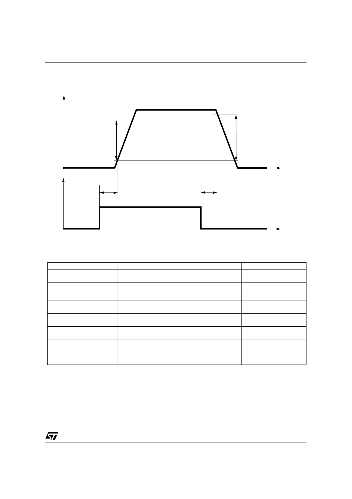
Switching time Waveforms
V
OUT
dV
/dt
OUT
(on)
V
IN
t
d(on)
80%
10%
t
d(off)
VN920D-B5 / VN920DSO
90%
dV
/dt
OUT
(off)
t
t
TRUTH TABLE
CONDITIONS INPUT OUTPUT STATUS
Normal Operation
Cur rent Limitatio n
Overtemperature
Undervoltage
Overvoltage
Output Voltage > V
Output Current < I
OL
OL
L
H
L
H
H
L
H
L
H
L
H
L
H
L
H
L
H
L
X
X
< T
(T
j
> T
(T
j
L
L
L
L
L
L
H
H
L
H
TSD
TSD
H
H
H
) H
) L
H
L
X
X
H
H
L
H
H
L
5/22
VN920D-B5 / VN920DSO
ELECTRICAL TRANSIENT REQUIREMENTS ON VCC PIN
ISO T/R 7637/1
Test Pulse
1 -25 V -50 V -75 V -100 V 2 m s 10 Ω
2 +25 V +50 V +75 V +100 V 0.2 ms 10 Ω
3a -25 V - 50 V -100 V -150 V 0.1 µs 50 Ω
3b +25 V +50 V +75 V +100 V 0.1 µs 50 Ω
4 -4 V -5 V -6 V -7 V 100 ms, 0.01
5 +26.5 V +46.5 V +66.5 V +86.5 V 400 ms, 2
ISO T/R 7637/1
Test P ulse
1CCCC
2CCCC
3aCCCC
3bCCCC
4CCCC
5CEEE
CLASS CONTENTS
C All functions of the device are performe d as designed after exposure to disturbance.
E One or more function s of the dev ice is not p erformed as design ed after ex posure to disturbance
and canno t be retur ned to proper operation without repla cing the device.
I II III IV Delays and
IIIIIIIV
TEST LEVELS
TEST LEVEL S RESULTS
Impedance
Ω
Ω
6/22
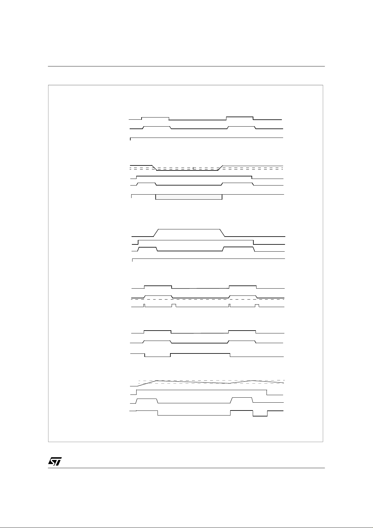
Figure1: Waveforms
INPUT
LOAD VOLTAGE
STATUS
V
CC
INPUT
LOAD VOLTAGE
STATUS
V
CC
INPUT
LOAD VOLTAGE
STATUS
NORMAL OPERATION
UNDERVOLTAGE
V
USD
OVERVOLTAGE
V
CC<VOV
V
USDhyst
undefined
VCC>V
VN920D-B5 / VN920DSO
OV
INPUT
LOAD VOLTAGE
STATUS
INPUT
LOAD VOLTAGE
STATUS
T
j
INPUT
LOAD CURRENT
STATUS
OPEN LOAD wi th external pull-up
V
OUT>VOL
V
OL
OPEN LOAD without external pull-up
T
TSD
T
R
OVERTEMPERATURE
7/22

VN920D-B5 / VN920DSO
APPLICATION SCHEMATIC
+5V
µ
R
C
R
prot
prot
+5V
STA T US
INPUT
GND PROTECTION NETWORK AGAINST
REVERSE BATTERY
Soluti on 1: Resistor in the ground line (R
can be us ed with any t ype of load.
The fo llowin g is an indica tion on how to dim ension the
resistor.
R
GND
1) R
2) R
where -I
be foun d in the abs olute max i mum rating se ct i on of the of
≤ 600mV / (I
GND
≥ (−VCC) / (-I
GND
is the DC re vers e grou nd pi n cu rren t an d can
GND
S(on)ma x
)
GND
).
the devic e’s datasheet.
Power Dissipation in R
battery situations) is:
= (-VCC)2/R
P
D
GND
(when VCC<0: during reverse
GND
This resistor can be shared amongst several different
HSD. Please note that the value of this resistor should be
calcul ated with form ula (1) wher e I
sum of the maximum on-state currents of the different
S(on)max
devices.
Please note that if the microprocessor ground is not
common with the device ground then the R
produce a shift (I
and the status output values. This shift will vary
S(on)max
* R
) in the input thresholds
GND
depending on many devices are ON in the case of several
high side drivers sharing the same R
GND
If the calculated power dissipation leads to a large resistor
or several devices hav e to share the sa me resisto r then
the ST suggest to utilize Solution 2 (see below).
Solution 2:
A resistor (R
D
GND
A diode (D
=1kΩ) sh ould b e insert ed in paral lel to
GND
if the device will be driving an inductive load.
) in the gr ound line.
GND
only). This
GND
becomes t he
GND
.
will
V
CC
D
OUTPUT
GND
R
V
GND
GND
D
GND
This small signal diode can be safely shared amongst
several different HSD. Also in this case, the presence of
j
the ground network wi ll produce a shift (
600mV) in t he
input threshold and the status output values if the
microprocessor ground is not common with the device
ground. This shift will not vary if more than one HSD
shares the same diode/resi stor net work.
LOAD DUMP PROTECTION
Dld is necessary (Voltage Transient Suppressor) if the
load dump peak voltage exceeds VCC max DC rating. The
same applies if the device will be subject to transients on
the VCC line that are grea ter tha n the ones sh own in the
ISO T/R 7637/1 table.
C I/Os PROTECTION:
µ
If a ground protection network is used and negative
transient are p resent on the VCC line, the control pins will
be pulled negative. ST suggests to insert a resistor (R
in lin e to prevent the µC I/Os pins to latch-up.
The value of these resistors is a compromise between the
leakage c urrent of µC an d the current required by the
HSD I/Os ( Input le vels comp atibilit y) wi th the lat ch-up li mit
of µC I/Os.
≤ R
-V
CCpeak/Ilatchup
Calculation example:
CCpeak
prot
= - 100V an d I
≤ 65kΩ.
prot
For V
5kΩ ≤ R
Recommended R
≤ (V
prot
OHµC-VIH-VGND
≥ 20mA; V
latchup
value is 10kΩ.
) / I
OHµC
ld
IHmax
≥ 4.5V
prot
)
8/22
1

VN920D-B5 / VN920DSO
Off State Output Current
IL(off1) (u A)
9
8
7
6
5
4
3
2
1
0
-50 -25 0 25 50 75 100 125 150 17 5
Tc (°C)
Input Clamp Voltage
Vicl (V)
8
7.8
7.6
7.4
7.2
7
6.8
6.6
6.4
6.2
6
Iin=1mA
-50 -25 0 25 50 75 100 125 150 175
Tc (°C)
High Level Input Current
Iih (uA)
5
4.5
3.5
2.5
1.5
0.5
Vin=3.25V
4
3
2
1
0
-50 -25 0 25 50 75 100 125 150 175
Input High Level
Vih (V)
3.6
3.4
3.2
3
2.8
2.6
2.4
2.2
2
-50 -25 0 25 50 75 100 125 150 175
Input Hysteresis VoltageInput Low Level
Tc (°C)
Tc (°C)
Vil (V)
2.6
2.4
2.2
2
1.8
1.6
1.4
1.2
1
-50 -25 0 25 50 75 100 125 150 175
Tc (°C)
Vhyst (V)
1.5
1.4
1.3
1.2
1.1
1
0.9
0.8
0.7
0.6
0.5
-50 -25 0 25 50 75 100 125 150 175
Tc (°C)
9/22
11

VN920D-B5 / VN920DSO
Overvoltage Shutdown
I
LIM
Vs. T
case
Vov (V)
50
48
46
44
42
40
38
36
34
32
30
-50 -25 0 25 50 75 100 125 150 175
Ilim (A)
100
90
80
70
60
50
40
30
20
10
Vcc=13V
0
-50 -25 0 25 50 75 100 125 150 175
Tc (°C)
Turn-on Voltage Slope Turn-off Voltage Slope
dVout/dt(on) (V/ms)
700
650
600
550
500
450
400
350
300
250
-50 -25 0 25 50 75 100 125 150 175
Vcc=13V
Rl=1.3Ohm
Tc (ºC)
dVout/dt(off) (V/ms)
550
500
450
400
350
300
250
200
150
100
50
Vcc=13V
Rl=1.3Ohm
0
-50 -25 0 25 50 75 100 125 150 175
Tc (ºC)
Tc (°C)
On State Resistance Vs. T
case
Ron (mOhm)
50
45
40
35
30
25
20
15
10
5
0
-50 -25 0 25 50 75 100 125 150 175
Iout=10A
Vcc=8V; 36V
Tc (ºC)
10/22
On State Resistance Vs. V
CC
Ron (mOhm)
50
45
40
35
30
25
20
15
10
5
0
5 10152025303540
Iout=10A
Tc=150ºC
Tc=25ºC
Tc= -40ºC
Vcc (V)

VN920D-B5 / VN920DSO
Status Leakage Current
Ilstat(µA)
0.05
0.045
0.04
0.035
0.03
0.025
0.02
0.015
0.01
0.005
Vstat=5V
0
-50 -25 0 25 50 75 100 125 150 175
Tc (ºC )
Status Low Output Voltage
Vstat (V)
0.8
0.7
0.6
0.5
Istat=1.6mA
Status Clamp Voltage
Vscl (V)
8
7.8
7.6
7.4
7.2
6.8
6.6
6.4
6.2
Istat=1mA
7
6
-50 -25 0 25 50 75 100 125 150 175
Tc (ºC)
0.4
0.3
0.2
0.1
0
-50 -25 0 25 50 75 100 125 150 175
Tc (ºC)
11/22

VN920D-B5 / VN920DSO
P2PAK Maximum turn off current versus load inductance
LMAX (A)
I
100
10
1
A
B
C
0.01 0.1 1 10 100
A = Single Pulse at T
B= Repetitive pulse at T
C= Repetitive Pulse at T
Conditions:
VCC=13.5V
Values are generated with RL=0Ω
In case of repetitive pulses, T
the temperature specified above for curves B and C.
VIN, I
L
=150ºC
Jstart
=100ºC
Jstart
=125ºC
Jstart
jstart
Demagnetization
(at beginning of each demagnetization) of every pulse must not exceed
L(mH)
Demagnetization
Demagnetization
12/22
t

SO-16L Maximum turn off current versus load inductance
LMAX (A)
I
100
10
C
VN920D-B5 / VN920DSO
A
B
1
0.01 0.1 1 10 100
A = Single Pulse at T
B= Repetitive pulse at T
C= Repetitive Pulse at T
Conditions:
VCC=13.5V
Values are generated with RL=0Ω
In case of repetitive pulses, T
the temperature specified above for curves B and C.
VIN, I
L
=150ºC
Jstart
=100ºC
Jstart
=125ºC
Jstart
jstart
Demagnetization
(at beginning of each demagnetization) of every pulse must not exceed
L(mH)
Demagnetization
Demagnetization
t
13/22

VN920D-B5 / VN920DSO
P2PAK PC Board
P2PAK THERMAL DATA
R
thj-amb
Layout conditio n of Rth and Zth measurements (PCB F R4 area= 60mm x 60mm, PCB thi ckness=2mm,
Cu thickness=35µm, Copper areas: 0.97cm
Vs. PCB copper area in open box free air condition
RTHj_amb (°C/W)
2
, 8cm2).
55
Tj-Tamb=50°C
50
45
40
35
14/22
30
0246810
PCB Cu heatsink area (cm^2)

SO-16L PC Board
VN920D-B5 / VN920DSO
SO-16L THERMAL DATA
R
thj-amb
Layout conditio n of Rth and Zth measur ements (P CB FR4 area= 41mm x 48mm , PCB thickness=2mm,
Cu thickness=35µm, Copper areas: 0.5cm
Vs. PCB copper area in open box free air condition
RTH j-amb (°C/W)
70
2
, 6cm2).
65
60
55
50
45
40
01234567
PCB Cu heatsink area ( cm ^2)
15/22

VN920D-B5 / VN920DSO
SO-16L Thermal Impedance Junction Ambient Single Pulse
ZTH (°C/W)
100
10
1
0.1
0.01
0.0001 0.001 0.01 0.1 1 10 100 1000
Time (s )
Thermal fitting model of a single channel HSD
in SO-16L
Pulse calculation formula
Z
THδ
where
RTHδ Z
δ tpT⁄=
THtp
Footprint
2
6 cm
1 δ–()+⋅=
Tj
16/22
C1
R1 R2
Pd
Thermal Parameter
Area/island (cm2) Footprint 6
R1 (°C/W) 0.02
C2
C3
R3
T_amb
C4
R4
C5
R5
C6
R6
R2 (°C/W) 0.1
R3 ( °C/W) 2.2
R4 (°C/W) 12
R5 (°C/W) 15
R6 (°C/W) 35 20
C1 (W.s/°C) 0.0015
C2 (W.s/°C) 7.00E-03
C3 (W.s/°C) 1.50E-02
C4 (W.s/°C) 0.14
C5 (W.s/°C) 1
C6 (W.s/°C) 5 8

P2PAK Thermal Impedance Junction Ambient Single Pulse
ZTH (°C/W)
1000
VN920D-B5 / VN920DSO
100
10
1
0.1
0.01
0.0001 0.001 0.01 0.1 1 10 100 1000
Time (s)
Thermal fitting model of a single channel HSD
in P2PAK
Pulse calculation formula
Z
THδ
where
RTHδ Z
δ tpT⁄=
THtp
Footprint
2
6 cm
1 δ–()+⋅=
Tj
Pd
C1
R1 R2
Thermal Parameter
Area/island (cm2) Footprint 6
R1 (°C/W) 0.02
C2
C3
R3
T_amb
C4
R4
C5
R5
C6
R6
R2 (°C/W) 0.1
R3 (°C/W) 0.22
R4 (°C/W) 4
R5 (°C/W) 9
R6 (°C/W) 37 22
C1 (W.s/°C) 0.0015
C2 (W.s/°C) 0.007
C3 (W.s/°C) 0.015
C4 (W.s/°C) 0.4
C5 (W.s/°C) 2
C6 (W.s/°C) 3 5
17/22

VN920D-B5 / VN920DSO
P2PAK MECHANICAL DATA
DIM.
A4.30 4.80
A1 2.40 2.80
A2 0.03 0.23
b0.80 1.05
c0.45 0.60
c2 1.17 1.37
D8.95 9.35
D2 8.00
E 10.00 10.40
E1 8.50
e3.20 3.60
e1 6.6 0 7.00
L 13.70 14.50
L2 1.2 5 1.40
L3 0.9 0 1.70
L5 1.5 5 2.40
R
V2 0º 8º
Package We ight 1.40 Gr (typ)
MIN. TYP MAX.
mm.
0.40
18/22
P010R

SO-16L MECHANICAL DATA
VN920D-B5 / VN920DSO
DIM.
A 2.65 0.104
a1 0.1 0.2 0.004 0.008
a2 2.45 0.096
b 0.35 0.49 0.014 0.019
b1 0.23 0.32 0.009 0.012
C 0.5 0.020
c1 45° (typ.)
D 10.1 10.5 0.397 0.413
E 10.0 10.65 0.39 3 0.419
e 1.27 0.050
e3 8.89 0.350
F 7.4 7.6 0.291 0.300
L 0.5 1.27 0.020 0.050
M 0.75 0.029
S8° (max.)
MIN. TYP MAX. MIN. TYP. MAX.
mm. inch
19/22
1111

VN920D-B5 / VN920DSO
10.8
9.4
4.6
16.15
2
P
PAK TUBE SHIPME NT (no suffix)P2PAK SUGGESTED PAD LAYOUT
Base Q.ty 50
Bulk Q.ty 1000
0.6
1.1
7.9
B
Tube length (± 0.5) 532
A 18
B 33.1
C
C (± 0.1) 1
All dimensions are in mm.
TAPE AND REEL SHIPMENT (suffix “13TR”)
TAPE DIMENSIONS
According to Elec tronic Industrie s Association
(EIA) Sta ndard 481 rev. A, Feb. 1986
Tape width W 24
Tape Hole Spacing P0 (± 0.1) 4
Component Spacing P 16
Hole Diameter D (± 0.1/-0) 1.5
Hole Diameter D1 (min) 1.5
Hole Position F (± 0.05) 11.5
Compartment Depth K (max) 6.5
Hole Spacing P1 (± 0.1) 2
A
All dimensions are in m m .
REEL DIMENSIONS
Base Q.ty 1000
Bulk Q.ty 1000
A (max) 330
B (min) 1.5
C (± 0.2) 13
F 20.2
G (+ 2 / -0) 24.4
N (min) 60
T (max) 30.4
All dimensions ar e in mm.
All dimensions ar e in mm.
20/22
1
Top
cover
tape
End
500mm min
Empty components pockets
saled with cover tape.
User direction of feed
Start
No componentsNo components Components
500mm min

VN920D-B5 / VN920DSO
SO-16L TUBE SHIPMENT (no suffix)
Base Q.ty 50
Bulk Q.ty 1000
C
A
B
TAPE AND REEL SHIPMENT (suffix “13TR”)
Tube length (± 0.5) 532
A 3.5
B 13.8
C (± 0.1) 0.6
All dimensions are in mm.
REEL DIMENSIONS
Base Q.ty 1000
Bulk Q.ty 1000
A (max) 330
B (min) 1.5
C (± 0.2) 13
F 20.2
G (+ 2 / -0) 16.4
N (min) 60
T (max) 22.4
TAPE DIMENSIONS
According to Elec tronic Industrie s Association
(EIA) Sta ndard 481 rev. A, Feb. 1986
Tape width W 16
Tape Hole Spacing P0 (± 0.1) 4
Component Spacing P 12
Hole Diameter D (± 0.1/-0) 1.5
Hole Diameter D1 (min) 1.5
Hole Position F (± 0.05) 7.5
Compartment Depth K (max) 6.5
Hole Spacing P1 (± 0.1) 2
All dimensions ar e in mm.
Top
cover
tape
End
500mm min
Empty components pockets
saled with cover tape.
User direction of feed
Start
No componentsNo components Components
500mm min
21/22
1

VN920D-B5 / VN920DSO
Information furnished is believed to be accurate and reliable. Ho wev er, STMicroelectr onics assumes no r es ponsibility for the consequences
of use of such information nor for any infringement of patents or other rights of third parties which may results from its use. No license is
granted by implication or otherwise under any patent or patent r ights of STMicr oelectronics . Specifications mentioned in this publication are
subject to c hange withou t notice. This publicatio n s upersedes an d r eplaces all information p r ev iously supplied. STMic r oelectroni c s pr oducts
are not authorized for use as critical components in life support devices or systems without express written approval of STMicroelectronics.
Australia - Brazil - Canada - Ch ina - Finland - France - Germany - Hong K ong - India - Isra el - Italy - Japan - M alaysia -
Malta - Moro c c o - S ingapore - Spain - Sweden - Switz er land - United Kingdom - U.S.A.
The ST logo is a trademark of ST M ic r oelectronic s
2003 STMicroelectronics - Printed in ITALY- All Rights Reserved.
STMicroelectronics GROUP OF COMPANIES
http://www.st.com
22/22
 Loading...