

SGS Thomson Microelectronics VN820SP13TR, VN820SP, VN820SO, VN820PT13TR, VN820PT Datasheet
...
®
VN820 / VN820SO
/ VN820SP / VN820-B5 / VN820PT
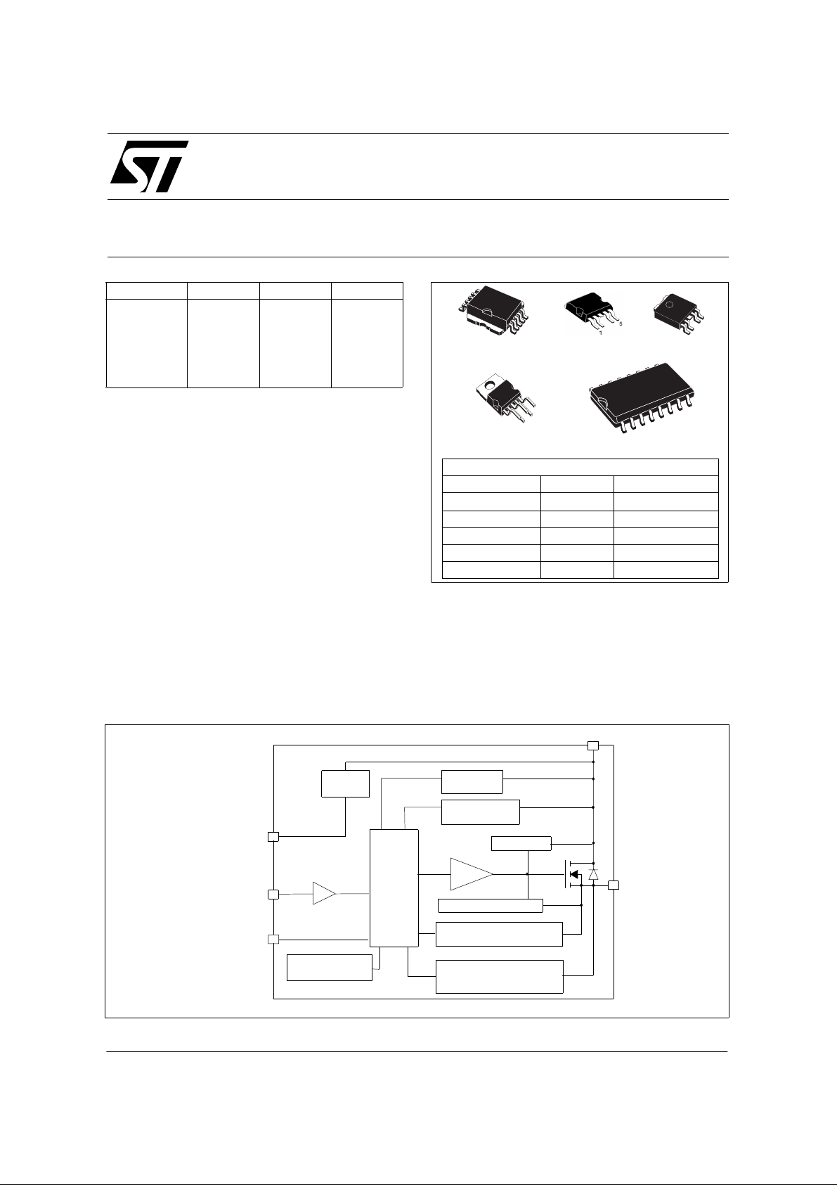
HIGH SIDE DRIVER
TYPE R
DS(on)
I
OUT
V
CC
VN820
VN820SP
VN820-B5
40 mΩ 9 A 36 V
VN820SO
VN820PT
■ CMOS COMPATIBLE INPUT
■ ON STATE OPEN LOAD DETECTION
■ OFF STATE OPEN LOAD DETECTION
■ SHORTED LOAD PROTECTION
■ UNDERVOLTAGE AND OVERVOLTAGE
SHUTDOWN
■ PROTECTION AGAINST LOSS OF GROUND
■ VERY LOW STAND-BY CURRENT
■ REVERSE BATTERY PROTECTION (*)
DESCRIPTION
The VN820, VN820SP, VN820-B5, VN820SO,
VN820PT are monoli thic devices made by using
STMicroelectronics VIPower M0-3 Technology,
intended for dri ving any kind of l oad wit h one side
connected to ground.
Active VCC pin voltage clamp prote cts the device
against low energy spikes (see ISO7637 transient
BLOCK DIAGRAM
10
1
PowerSO-10™
PENTAWATT
P2PAK
SO-16L
PPAK
ORDER CODES
PACKAGE TUBE T&R
PENTAWATT
VN820
PowerSO-10™ VN820SP VN820SP13TR
P2PAK VN820-B5 VN820-B513TR
SO-16L VN820SO VN820SO13TR
PPAK VN820PT VN820PT13TR
compatibility table). Active current limitation
combined with thermal shutdown and automatic
restart protect the device against overload.
The device detects open load condition both is on
and off state. Output shorted to VCC is detected in
the off state. Device automatically turns off in case
of ground pin disconnection.
V
CC
OVERVOLTAGE
DETECTION
UNDERVOLTAGE
DETECTION
Power CLAMP
DRIVER
CURRENT LIMITER
ON STATE OPENLOAD
DETECTION
OFF STATE OPENLOAD
AND OUTPUT SHORTED TO V
DETECTION
OUTPUT
CC
GND
INPUT
STATUS
(*) See application schematic at page 9
V
CC
CLAMP
OVERTEMPERATURE
DETECTION
LOGIC
June 20 03 1/34
VN820 / VN820SO / VN820SP / VN820-B5 / VN820PT
ABSOLUTE MAXIMUM RATI NG
Symbol Parameter
DC Supply Vol tage 41 V
V
CC
- V
- I
- I
I
Reverse DC Supply Volt age - 0.3 V
CC
DC Reverse Ground Pin Current - 200 mA
GND
DC Output Current Internally Limited A
I
OUT
Reverse DC Ou tput Current - 9 A
OUT
DC Input Current +/- 10 mA
I
IN
DC Status Curr ent +/- 10 mA
STAT
Electrostatic Discharge
(Human Bo dy Model: R=1 .5KΩ; C=100pF)
ESD
- INPUT
- STATUS
V
- OUTPUT
- V
CC
E
E
E
Maximum Switching Energy (L=4mH; RL=0Ω;
MAX
V
=13.5V ; T
bat
Maximum Switching Energ y (L=3 .7mH;
MAX
RL=0Ω; V
Maximum Switching Energy (L=4.48mH;
MAX
RL=0Ω; V
Power Diss ip ation TC=25°C 65.8 65.8 65.8 8.3 65.8 W
P
tot
Junction Operating Temperature Internally Limited °C
T
j
Case Oper ating Temperature - 40 to 150 °C
T
c
Storage Temperature - 55 to 150 °C
T
stg
jstart
=13.5V ; T
bat
=13.5V ; T
bat
=150ºC ; IL=13A)
=150ºC ; IL=13A)
jstart
=150ºC ; IL=13A)
jstart
PowerSO-10
481 481 mJ
Value
™ PENTAWATT P
4000
4000
5000
5000
2
PAK SO-16L PPAK
438 mJ
526 mJ
Unit
V
V
V
V
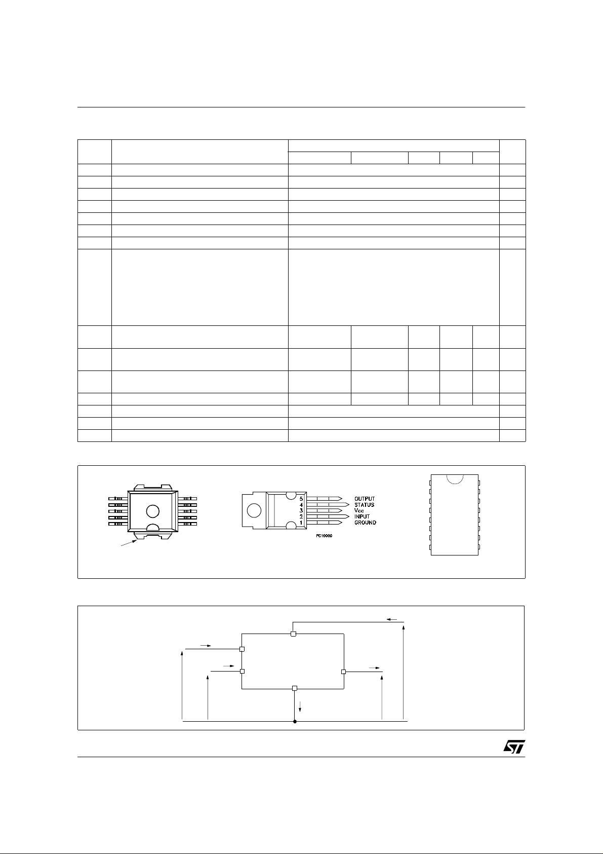
CONNECTION DIAGRAM (TOP VIEW)
GROUND
INPUT
STATUS
N.C.
N.C.
6
7
8
9
10
V
CC
PowerSO-10
5
4
3
2
1
11
™
OUTPUT
OUTPUT
N.C.
OUTPUT
OUTPUT
PPAK / P2PAK / PENTAWATT
CURRENT AND VOLTAGE CONVENTIONS
I
IN
I
STAT
V
IN
V
STAT
INPUT
STATUS
V
CC
GND
OUTPUT
I
GND
I
OUT
V
N.C.
GND
INPUT
STATUS
N.C.
N.C.
V
V
OUT
CC
CC
1
8
V
16
CC
OUTPUT
OUTPUT
OUTPUT
OUTPUT
OUTPUT
OUTPUT
V
9
CC
SO-16L
I
S
V
CC
2/34
VN820 / VN820SO / VN820SP / VN820-B5 / VN820PT
THERMAL DATA
Symbol Parameter
R
thj-case
R
thj-lead
R
thj-amb
(*) When mounted on a standard single-sided FR-4 boar d with 0.5cm2 of Cu (at leas t 35µ m t hick) .
(**) When mounted on FR4 printed circuit board with 0.5cm
Thermal Resistance Junction-case Max 1.9 1.9 1.9 - 1.9 °C/W
Thermal Resistance Junction-lead Max - - - 15 - °C /W
Thermal Resistance Junction-ambient Max 51.9 (*) 61.9 (*) 51.9 (*) 6 5 (**) 76.9 (*) °C/W
PowerSO-10
2
of Cu (at leas t 35µ thick) connec ted to all VCC pins.
ELECTRICAL CHARACTERISTICS (8V<VCC<36V; -40°C<Tj<150°C unless otherwise specified)
POWER
Symbol Parameter Test Conditions Min Typ Max Unit
CC
OV
ON
S
Oper ating Su pp ly Voltag e 5.5 13 36 V
Undervolt age Shut- down 3 4 5.5 V
Undervolt age Shut- down
hysteresis
Overvolt age Shut-d own 36 V
=3A; Tj=25°C; VCC>8V
I
On State Resistance
Supply Current
Off State Output Curr ent VIN=V
Off State Output Curr ent VIN=0V; V
Off State Output Curr ent VIN=V
Off State Output Curr ent VIN=V
OUT
I
=3A; VCC>8V
OUT
Off Stat e; V
Off Stat e; V
Tj=25°C
On State; V
OUT
OUT
OUT
=13V; VIN=V
CC
=13V; VIN=V
CC
=13V; VIN=5V; I
CC
=0V 0 50 µA
=3.5V -75 0 µA
OUT
=0V; Vcc=13V; Tj =125°C 5 µA
=0V; Vcc=13V; Tj =25°C 3 µ A
V
V
USD
V
USDhyst
V
R
I
I
L(off1)
I
L(off2)
I
L(off3)
I
L(off4)
Value
™ PENTAWATT P
=0V
OUT
=0V;
OUT
=0A
OUT
2
PAK SO-16L PPAK
0.5 V
40
80
10
10
2
25
20
3.5
Unit
mΩ
mΩ
µA
µA
mA
SWITCHING (VCC=13V)
Symbol Parameter Test Conditions Min Typ Max Unit
RL=4.3Ω from VIN rising ed ge to
V
=1.3V
OUT
RL=4.3Ω from VIN falling edge to
V
=11.7V
OUT
RL=4.3Ω from V
V
=10.4V
OUT
RL=4.3Ω from V
V
=1.3V
OUT
OUT
OUT
=1.3 to
=11.7 to
30 µs
30 µs
See
relative
diagram
See
relative
diagram
dV
dV
t
d(on)
t
d(off)
OUT
OUT
Turn-on Delay Time
Turn-off Delay Tim e
/dt
Turn-on Voltage Slope
(on)
/dt
Turn-off Voltage Slope
(off)
INPUT PIN
Symbol Parameter Test Conditions Min Typ Max Unit
Input Low Level 1.25 V
IL
Low Level Input Current VIN=1.25V 1 µA
IL
Input High Level 3.25 V
IH
High Level Input Current VIN=3.25V 10 µA
Input Hysteresis Voltage 0.5 V
Input Clamp Voltage
I
IN
I
IN
=1mA
=-1mA
66.8
-0.7
8V
V
V
V
I
V
I
IH
I(hyst)
ICL
V/µs
V/µs
V
3/34
1
VN820 / VN820SO / VN820SP / VN820-B5 / VN820PT
ELECTRICAL CHARACTERISTICS (continued)
STATUS PIN
Symbol Parameter Test Conditions Min Typ Max Unit
V
STAT
I
LSTAT
C
STAT
V
SCL
Status Low Output Voltage I
Status Leakage Current Normal Operation V
Status Pin Input
Capacitance
Status Clamp Voltage
PROTECTIONS
Symbol Parameter T est Conditions Min Typ Max Unit
T
T
t
V
demag
TSD
T
hyst
SDL
I
lim
Shut-down Temperature 150 175 200 °C
Reset Temp erature 135 °C
R
Ther ma l Hy steres is 7 15 °C
Statu s delay in ov erload
condition
Current limitation
Turn-off Output Clamp
Voltage
=1.6mA 0.5 V
STAT
Normal Operation V
=1mA
I
STAT
I
=-1mA
STAT
T
j>TTSD
=5V 10 µA
STAT
=5V 100 pF
STAT
66.8
-0.7
20 µs
9132020A
5.5V<V
I
OUT
<36V
CC
=3A; VIN=0V; L= 6m H VCC-41 VCC-48 VCC-55 V
8V
V
A
OPENLOAD DETECTION
Symbol Parameter Test Conditions Min Typ Max Unit
OL
Openload ON State
Detectio n Threshold
Openload ON State
Detection Delay
Openload OFF State
Voltage Det ection
Threshold
Openl o ad Detect ion De l a y
at Turn Off
V
> V
OUT
=5V 70 150 300 mA
V
IN
=0A 200 µs
I
OUT
V
=0V 1.5 2.5 3.5 V
IN
OVERTEMP STATUS TIMING
I
< I
OUT
OL
OL
V
V
IN
STAT
Tj > T
TSD
1000 µs
I
OL
t
DOL(on)
V
t
DOL(off)
OPEN LOAD STATUS TIMING (with external pull-up)
V
IN
V
STAT
4/34
2
t
DOL(off)
t
DOL(on)
t
SDL
t
SDL
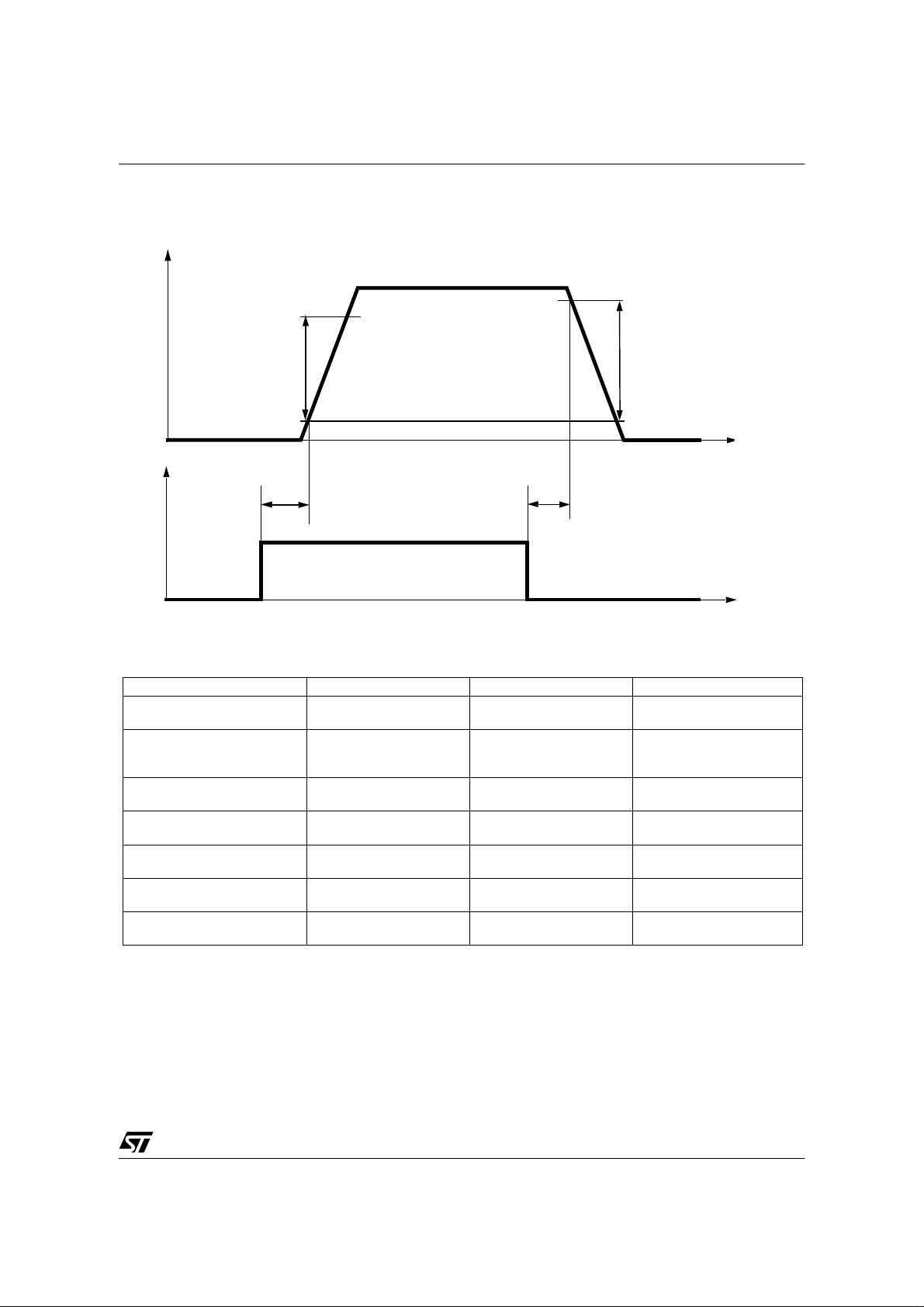
Switching time Waveforms
V
OUT
dV
/dt
OUT
(on)
V
IN
t
d(on)
80%
VN820 / VN820SO / VN820SP / VN820-B5 / VN820PT
90%
dV
/dt
OUT
(off)
10%
t
t
d(off)
t
TRUTH TABLE
CONDITIONS INPUT OUTPUT STATUS
Normal Operation
Current Limitation
Overtemperature
Undervo l tage
Overvoltage
Output Voltage > V
Output Current < I
OL
OL
L
H
L
H
H
L
H
L
H
L
H
L
H
L
H
L
H
L
X
X
(T
(T
< T
j
> T
j
L
L
L
L
L
L
H
H
L
H
TSD
TSD
H
H
H
) H
) L
H
L
X
X
H
H
L
H
H
L
5/34
VN820 / VN820SO / VN820SP / VN820-B5 / VN820PT
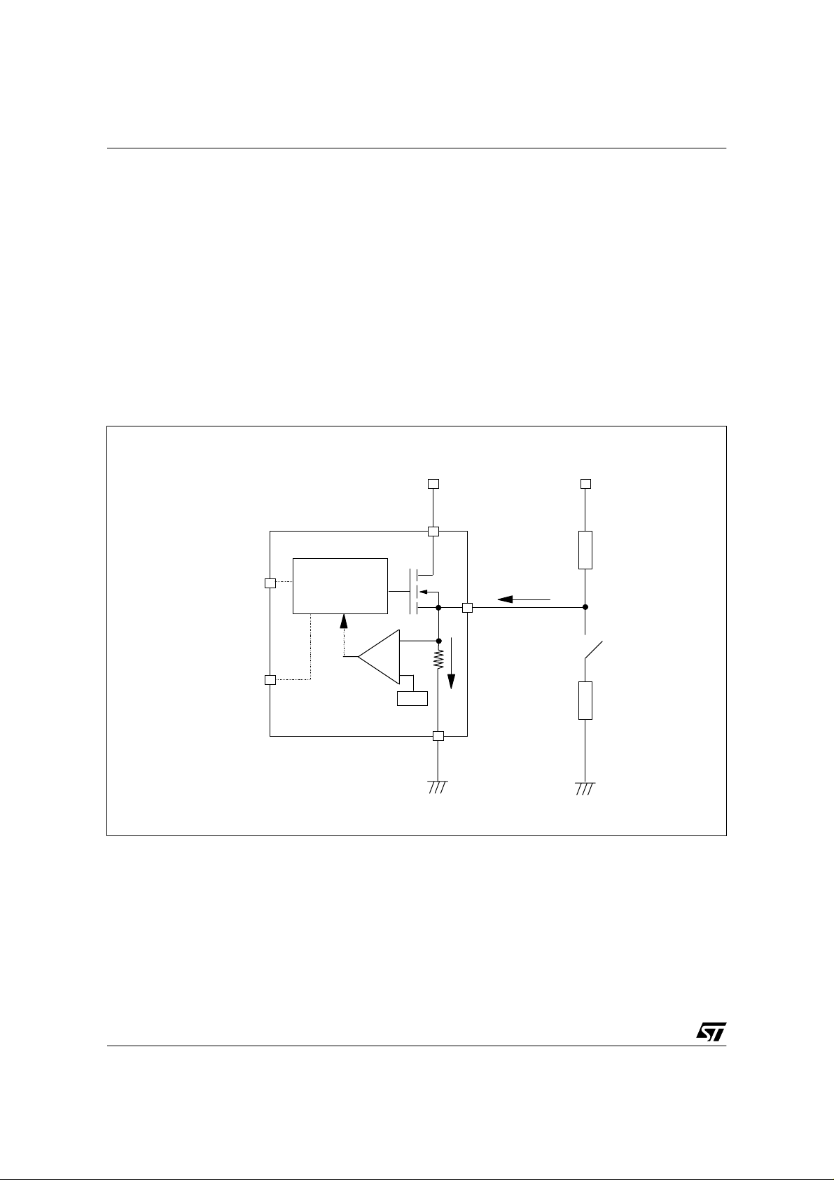
OPEN LOAD DETECTION IN OFF STATE
Off state open load detection requires an external pull-up
resistor (R
positive supply voltage (V
) connected between OUTPUT pin and a
PU
) like the +5 V line used to
PU
supply the microprocessor.
The external resistor has to be selected according to the
following requirements:
1) no f al se op en load i nd icat ion wh en load i s co nne cted :
in thi s case we have to avoi d V
V
; this res ults in the following condition
Olmin
=(VPU/(RL+RPU))RL<V
V
OUT
to be hi gher than
OUT
Olmin.
Open Load detection in off state
INPUT
DRIVER
+
LOGIC
2) no misdetection when load is disconnected: in this
case the V
results in the following condition R
I
.
L(off2)
Beca us e I
s(OFF)
has to be higher than V
OUT
<(V
PU
may si gn ifi c a ntly increase if V
high (up t o several mA ), the pul l-up resi stor R
be conne cted t o a su pp ly t ha t is swit ch ed OFF when t h e
module is in standby.
The values of V
OLmin
, V
OLmax
and I
are available in
L(off2)
the Electrical Characteri stics sec ti on.
V batt. VPU
CC
V
PU
R
L(off2)
I
; this
OLmax
PU–VOLma x
is pulled
out
should
PU
)/
STATUS
+
-
OL
V
GROUND
OUT
R
L
R
6/34
VN820 / VN820SO / VN820SP / VN820-B5 / VN820PT
ELECTRICAL TRANSIENT REQUIREMENTS ON VCC PIN
ISO T/R 7637/1
Test Pulse
1 -25 V -50 V -75 V -100 V 2 ms 10 Ω
2 +25 V +50 V +75 V +100 V 0.2 ms 10 Ω
3a -25 V -50 V -100 V -150 V 0.1 µs 50 Ω
3b +25 V +50 V +75 V +100 V 0.1 µs 50 Ω
4 -4 V -5 V -6 V -7 V 100 ms, 0.01
5 +26.5 V +46.5 V +66.5 V +86.5 V 400 ms, 2
ISO T/R 7637/1
Test Pulse
1CCCC
2CCCC
3aCCCC
3bCCCC
4CCCC
5CEEE
CLASS CONTENTS
C All functions of the device are performed as de signed after exposure to disturbance.
E One or more f unctions of the device is not performed as d esigned af ter expos ure to disturbance
and cann ot be returned to proper operat ion without replacing the device.
I II III IV D el ay s and
I II III IV
TEST LEVELS
TEST LEVELS R ESULTS
Impedance
Ω
Ω
7/34
VN820 / VN820SO / VN820SP / VN820-B5 / VN820PT
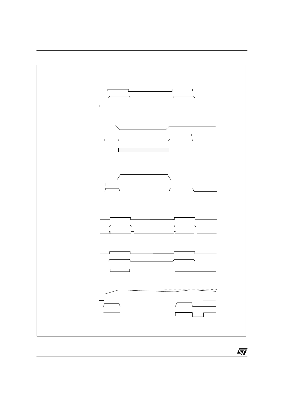
Figur e 1: Waveforms
NORMAL OPERATION
INPUT
LOAD VOLTAGE
STATUS
UNDERVOLTAGE
V
CC
INPUT
LOAD VOLTAGE
STATUS
V
CC
INPUT
LOAD VOLTAGE
STATUS
V
V
CC<VOV
USD
OVERVOLTAGE
V
USDhyst
undefined
VCC>V
OV
INPUT
LOAD VOLTAGE
STATUS
INPUT
LOAD VOLTAGE
STATUS
T
j
INPUT
LOAD CURRENT
STATUS
OPEN LOAD wi th external pull-up
V
OUT>VOL
V
OL
OPEN LOAD without external pull-up
T
T
TSD
R
OVERTEMPERATURE
8/34

APPLICATION SCHEMATIC
VN820 / VN820SO / VN820SP / VN820-B5 / VN820PT
+5V
µ
R
C
R
prot
prot
+5V
STA T US
INPUT
GND PROTECTION NETWORK AGAINST
REVERSE BATTERY
Soluti on 1: Resistor in the ground line (R
can be us ed with any type of load .
The fo llowin g is an indicati on on how to dimen sion the
resistor.
R
GND
1) R
2) R
where -I
be foun d in the absolute m aximum rating se ction of the of
≤ 600mV / (I
GND
≥ (−VCC) / (-I
GND
is the DC re vers e grou nd pi n cu rren t an d can
GND
S(on)ma x
)
GND
).
the devic e’s datasheet.
Power Dissipation in R
battery situations) is:
= (-VCC)2/R
P
D
GND
(when VCC<0: during reverse
GND
This resistor can be shared amongst several different
HSD. Please note that th e va l u e of this re sistor should be
calcul ated with form ula (1) wher e I
sum of the maximum on-state currents of the different
S(on)max
devices.
Please note that if the microprocessor ground is not
common with the device ground then the R
produce a shift (I
and the status output values. This shift will vary
S(on)max
* R
) in the input thresholds
GND
depending on many devices are ON in the case of several
high side drivers sharing the same R
GND
If the calculated power dissipation leads to a large resistor
or several devices hav e to share the sa me resisto r then
the ST suggest to uti lize Solution 2 (see be low).
Solution 2:
A resistor (R
D
GND
A diode (D
=1kΩ) sh ould b e insert ed in paral lel to
GND
if the device will be driving an inductive load.
) in the gr ound line .
GND
only). This
GND
becomes t he
GND
.
will
V
CC
D
OUTPUT
GND
R
V
GND
GND
D
GND
This small signal diode can be s afely shared amongst
several different HSD. Also in this case, the presence of
j
the ground network wi ll produce a shift (
600mV) in t he
input threshold and the status output values if the
microprocessor ground is not common with the device
ground. This shift will not vary if more than one HSD
shares the same diode/resistor network.
LOAD DUMP PROTECTION
Dld is necessary (Voltage Transient Suppressor) if the
load dump peak voltage exceeds VCC max DC rating. The
same applies if the devic e will be subject to transients on
the VCC line that are grea ter tha n the ones sh own in the
ISO T/R 7637/1 table.
C I/Os PROTECTION:
µ
If a ground protection network is used and negative
transient are present on the VCC line, the control pins will
be pulled negative. ST suggests to insert a resistor (R
in lin e to prevent the µC I/Os pins to latch-up.
The value of these resistors is a compromise between the
leakage c urrent of µC an d the current required by the
HSD I/Os ( Input le vels comp atibilit y) wi th the lat ch-up li mit
of µC I/Os.
≤ R
-V
CCpeak/Ilatchup
Calculation exam ple:
CCpeak
prot
= - 100V an d I
≤ 65kΩ.
prot
For V
5kΩ ≤ R
Recommended R
≤ (V
prot
OHµC-VIH-VGND
≥ 20 mA; V
latchup
value is 10kΩ.
) / I
OHµC
ld
IHmax
≥ 4.5V
prot
)
9/34
1
1
VN820 / VN820SO / VN820SP / VN820-B5 / VN820PT
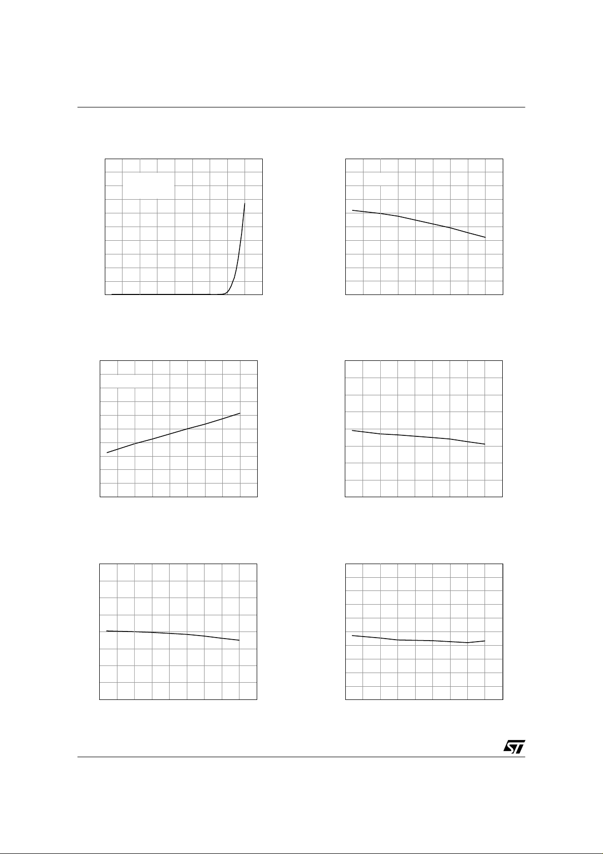
Off State Output Current
IL(off1) (µ A)
5
4.5
4
3.5
3
2.5
2
1.5
1
0.5
0
-50 -25 0 25 50 75 100 125 150 175
Off state
Vcc=36V
Vin=Vout=0V
Tc (ºC)
Input Clamp Voltage
Vicl (V)
8
7.8
7.6
7.4
7.2
7
6.8
6.6
6.4
6.2
6
Iin=1mA
-50 -25 0 25 50 75 100 125 150 175
Tc (°C)
High Level Input Current
Iih (uA)
5
4.5
3.5
2.5
1.5
0.5
Vin=3.25V
4
3
2
1
0
-50 -25 0 25 50 75 100 125 150 175
Input High Level
Vih (V)
3.6
3.4
3.2
3
2.8
2.6
2.4
2.2
2
-50 -25 0 25 50 75 100 125 150 175
Input Hysteresis VoltageInput Low Level
Tc (°C)
Tc (°C)
Vil (V)
2.6
2.4
2.2
2
1.8
1.6
1.4
1.2
1
-50 -25 0 25 50 75 100 125 150 175
Tc (°C)
10/34
Vhyst (V)
1.5
1.4
1.3
1.2
1.1
1
0.9
0.8
0.7
0.6
0.5
-50 -25 0 25 50 75 100 125 1 50 175
Tc (°C)
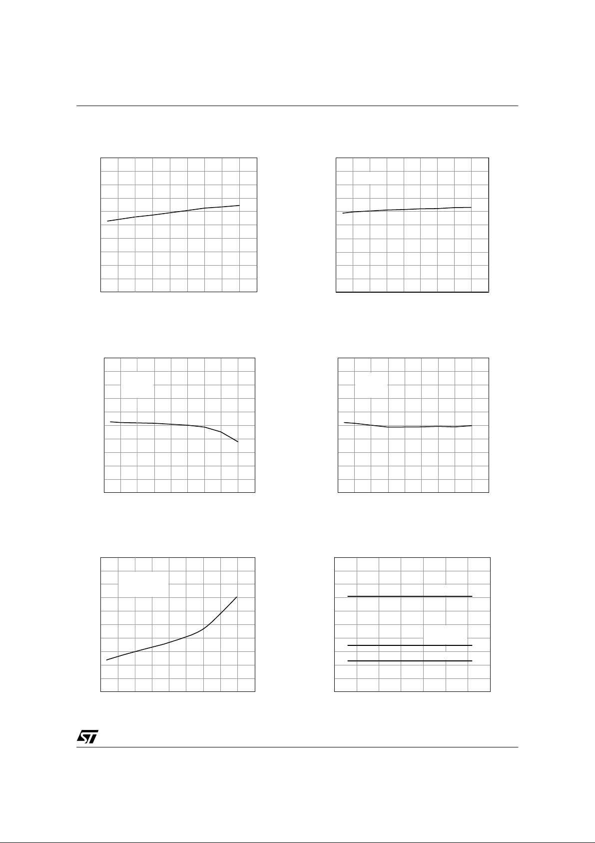
Overvoltage Shutdown
VN820 / VN820SO / VN820SP / VN820-B5 / VN820PT
I
Vs T
LIM
case
Vov (V)
50
48
46
44
42
40
38
36
34
32
30
-50 -25 0 25 50 75 100 125 150 175
Ilim (A)
25
22.5
20
17.5
15
12.5
10
7.5
5
2.5
0
Vcc=13V
-50 -25 0 25 50 75 100 125 150 175
Tc (°C)
Turn-on Voltage Slope Turn-off Voltage Slope
dVout/dt(on) (V/ms)
1000
900
800
700
600
500
400
300
200
100
Vcc=13V
Rl=4.3Ohm
0
-50 -25 0 25 50 75 100 125 150 175
Tc (ºC)
dVout/dt(off) (V/ms)
1000
900
800
700
600
500
400
300
200
100
Vcc=13V
Rl=4.3Ohm
0
-50 -25 0 25 50 75 100 125 150 175
Tc (ºC)
Tc (ºC)
On State Resistance Vs T
case
Ron (mOhm)
100
90
80
70
60
50
40
30
20
10
0
-50 -25 0 25 50 75 100 125 150 175
Iout=3A
Vcc=8V; 13V; 36V
Tc (ºC)
1
On State Resistance Vs V
CC
Ron (mOhm)
100
90
80
70
60
50
40
30
20
10
0
5 10152025303540
Tc= 150ºC
Tc= 25ºC
Tc= - 40ºC
Vcc (V)
11/34
 Loading...