

®
July 2002 1/21
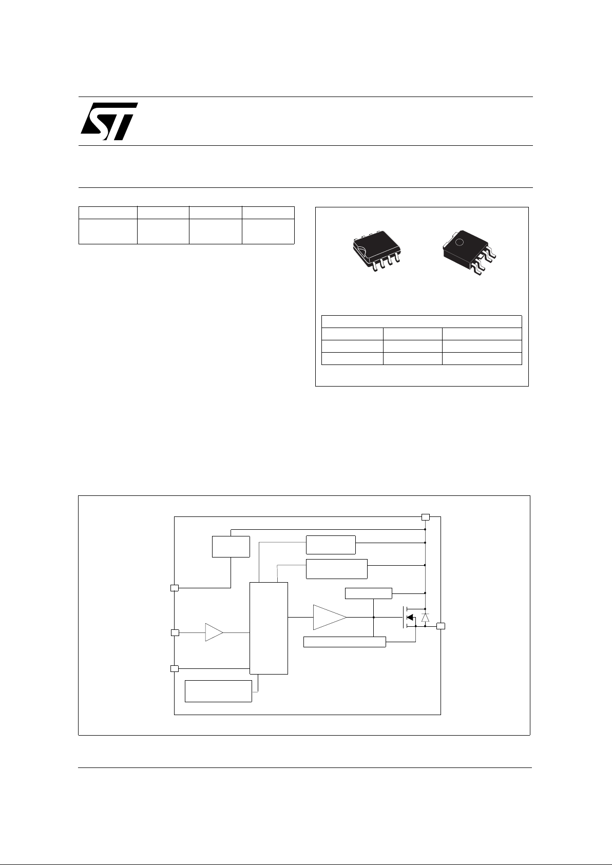
VN800S
/ VN800P T
HIGH SIDE DRIVER
1
■ CMOS COMPATIBLE INPUT
■ THERMAL SHUTDOWN
■ CURRENT LIMITATION
■ SHORTED LOAD PROTECTION
■ UNDERVOLTAGE AND OVERVOLTAGE
SHUTDOWN
■ PROTECTION AGAINST LOSS OF GROUND
■ VERY LOW STAND-BY CURRENT
■ REVERSE BATTERY PROTECTION (*)
DESCRIPTION
The VN800S, VN800PT are monolithic devices
made by using STMicroelectronics VIPower M0-3
Technology, i ntended for dr iving any ki nd of load
with one side connected to ground.
Active VCC pin voltage clamp protec ts the device
against low energy spikes. Active current
limitation combined with thermal shutdown and
automatic restart protect the device against
overload. Device automatically turns off in case of
ground pin disconnection. This device is
especially suitable for industrial applications in
norms conformity with IEC1131 (Programmable
Controllers International Standard).
TYPE R
DS(on)
I
OUT
V
CC
VN800S
VN800PT
135 mΩ 0.7 A 36 V
ORDER CODES
PACKAGE TUBE T&R
SO-8 VN800S VN800S13TR
PPAK VN800PT VN800PT13TR
SO-8 PPAK
BLOCK DIAGRAM
UNDERVOLTAGE
OVERTEMPERATURE
GND
INPUT
OUTPUT
OVERVOLTAGE
CURRENT LIMITER
LOGIC
DRIVER
Power CLAMP
STATUS
V
CC
CLAMP
DETECTION
DETECTION
DETECTION
(*) See note at page 7
V
CC
2/21
VN800S / VN800PT
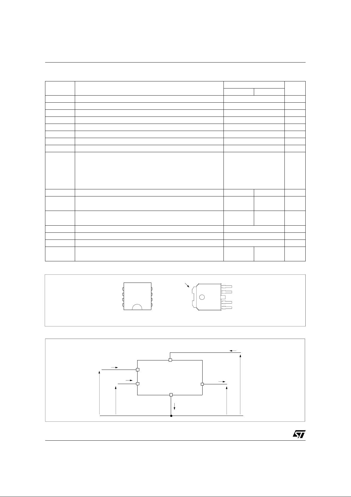
ABSOLUTE MAXIMUM RATI NG
CONNECTION DIAGRAM (TOP VIEW)
CURRENT AND VOLTAGE CONVENTIONS
Symbol Parameter
Value
Unit
SO-8 PPAK
V
CC
DC Supply Voltag e 41 V
- V
CC
Reverse DC Supply Voltage - 0.3 V
- I
GND
DC Reverse Ground Pin Current - 200 mA
I
OUT
DC Output Current Internally Limited A
- I
OUT
Reverse DC Output Current - 6 A
I
IN
DC Input Current +/- 10 mA
V
IN
Input Vol t age Range -3/+V
CC
V
V
STAT
DC Status Vol tage + V
CC
V
V
ESD
Electro static Discharge (H um an Body Model: R=1.5KΩ; C=100p F)
- INPU T
- STATUS
- OUTPU T
- V
CC
4000
4000
5000
5000
V
V
V
V
P
tot
Powe r Dissip at ion TC=25°C 4.2 41.7 W
E
MAX
Maximum Switching Energy
(L=77.5mH; R
L
=0Ω; V
bat
=13.5V ; T
jstart
=150ºC ; IL=1.5A)
121 mJ
E
MAX
Maximum Switching Energy
(L=125mH; R
L
=0Ω; V
bat
=13.5V; T
jstart
=150ºC; IL=1.5A)
195 mJ
T
j
Junction Operati ng Temperature Internally Limit ed °C
T
c
Case Operating Temperature - 40 to 150 °C
T
stg
Storage Temperature - 55 to 150 °C
L
max
Max Induc ti ve Load (VCC=30V; I
LOAD
=0.5A; T
amb
=100°C;
Rth
case>ambient
≤25°C/W)
2H
1
V
CC
V
CC
OUTPUT
OUTPUT
N.C.
GND
STATUS
INPUT
1
4
5
8
5
4
3
2
1
STATUS
OUTPUT
GND
INPUT
V
CC
SO-8 PPAK
INPUT
I
S
I
IN
V
IN
V
CC
STATUS
I
STAT
V
STAT
GND
V
CC
I
OUT
V
OUT
I
GND
OUTPUT
3/21
VN800S / VN800PT
THERMAL DATA
(*) When mounted on FR4 printed circuit board with 0.5 cm2 of copper area ( at least 35µ thick) connected to all VCC pins.
(**) When mounted on FR4 printed circuit board with 0.5 cm
2
of copper area ( at least 35µ thick).
ELECTRICAL CHARACTERISTICS (8V<VCC<36V; -40°C<Tj<150°C, unless otherwise specified)
POWER
SWITCHING (VCC=24V)
INPUT PIN
Symbol Parameter
Value
Unit
SO-8 PPAK
R
thj-case
Thermal R esistanc e Junctio n-case
Max
-3°C/W
R
thj-lead
Thermal R esistanc e Junctio n-lead
Max
30 - °C/W
R
thj-amb
Thermal R esistanc e Junctio n-ambient
Max
93 (*) 78 (**) °C/W
Symbol Parameter Test Conditions Min Typ Max Unit
V
CC
Operating Supply Voltage 5.5 36 V
V
USD
Undervolt age Shut- down 3 4 5.5 V
V
OV
Overvolt age Shut-down 36 42 V
R
ON
On State Resistance
I
OUT
=0.5A; Tj=25°C
I
OUT
=0.5A
135
270
mΩ
mΩ
I
S
Supply Current
Off State; V
CC
=24V; T
case
=25°C
On State; V
CC
=24V
On State; V
CC
=24V; T
case
=100°C
10
1.5
20
3.5
2.6
µA
mA
mA
I
LGND
Output Current at turn-off
V
CC=VSTAT=VIN=VGND
=24V
V
OUT
=0V
1mA
I
L(off1)
Off State Output Current VIN=V
OUT
=0V 0 50 µA
I
L(off2)
Off State Output Current VIN=V
OUT
=0V; Vcc=13V; Tj =125°C 5 µA
I
L(off3)
Off State Output Current VIN=V
OUT
=0V; Vcc=13V; Tj =25°C 3 µA
Symbol Parameter Test Conditions Min Typ Max Unit
t
d(on)
Turn-on Delay Time
RL=48Ω from VIN rising edge to
V
OUT
=2.4V
10 µs
t
d(off)
Turn-off Delay Time
RL=48Ω from VIN falli ng edge to
V
OUT
=21.6V
40 µs
dV
OUT
/
dt
(on)
Turn-on Voltage Slope
RL=48Ω from V
OUT
=2.4V to
V
OUT
=19.2V
See
relativ e
diagram
V/µs
dV
OUT
/
dt
(off)
Turn-off Volta ge Slope
RL=48Ω from V
OUT
=21.6V to
V
OUT
=2.4V
See
relative
diagram
V/µs
Symbol Paramete r Test Conditions Min Typ Max Unit
V
INL
Input Low Level 1.25 V
I
INL
Low Leve l Input Curr ent VIN=1.25V 1 µA
V
INH
Input High Level 3.25 V
I
INH
High Level Input Current VIN=3.25V 10 µA
V
I(hyst)
Input Hysteres is Voltag e 0.5 V
I
IN
Input Current VIN=VCC=36V 200 µA
1
4/21
VN800S / VN800PT
2
ELECTRICAL CHARACTERISTICS (continued)
STATUS PIN
PROTECTIONS
Symbol Parameter Test Conditions Min Typ Max Unit
V
STAT
Status Low Output Voltage I
STAT
=1.6 mA 0.5 V
I
LSTAT
Status Leakage Current Normal Operation; V
STAT=VCC
=36 V 10 µA
C
STAT
Status Pin Input
Capacitance
Normal Operation; V
STAT
= 5V 30 pF
Symbol Parame ter Test Conditi ons Min Typ Max Unit
T
TSD
Shut-down Temperature 150 175 200 °C
T
R
Reset Temp erature 135 °C
T
hyst
Ther ma l Hy steresis 7 15 °C
T
SDL
Status Delay in Overload
Condition
T
j>Tjsh
20 µs
I
lim
DC Short Circuit Current VCC=24V; R
LOAD
=10mΩ 0.7 2 A
V
demag
Turn-off Output Clamp
Voltage
I
OUT
=0.5 A; L=6mH VCC-47 VCC-52 VCC-57 V
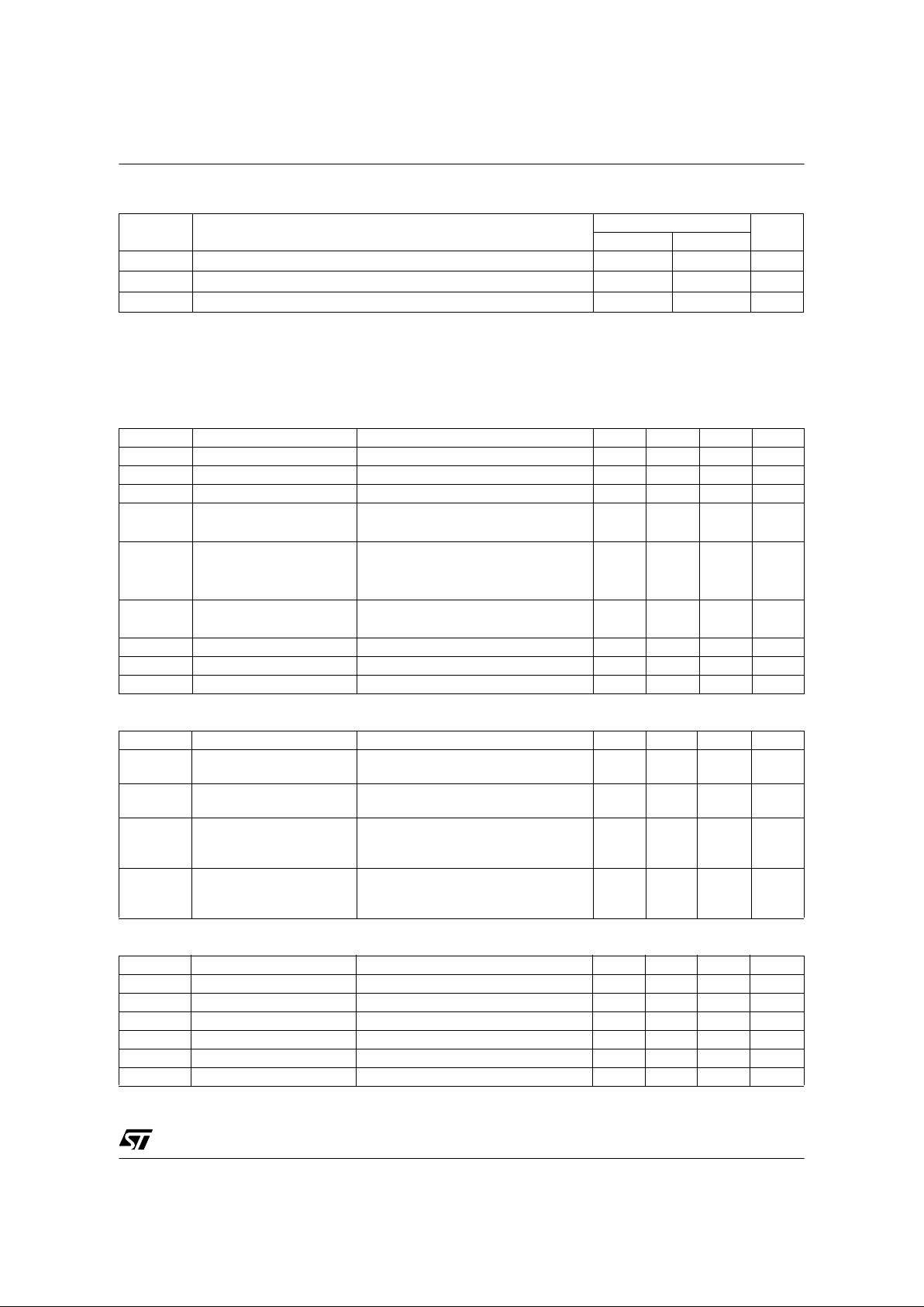
OVERTEMP STATUS TIMING
Tj>T
jsh
V
IN
V
STAT
t
SDL
t
SDL
5/21
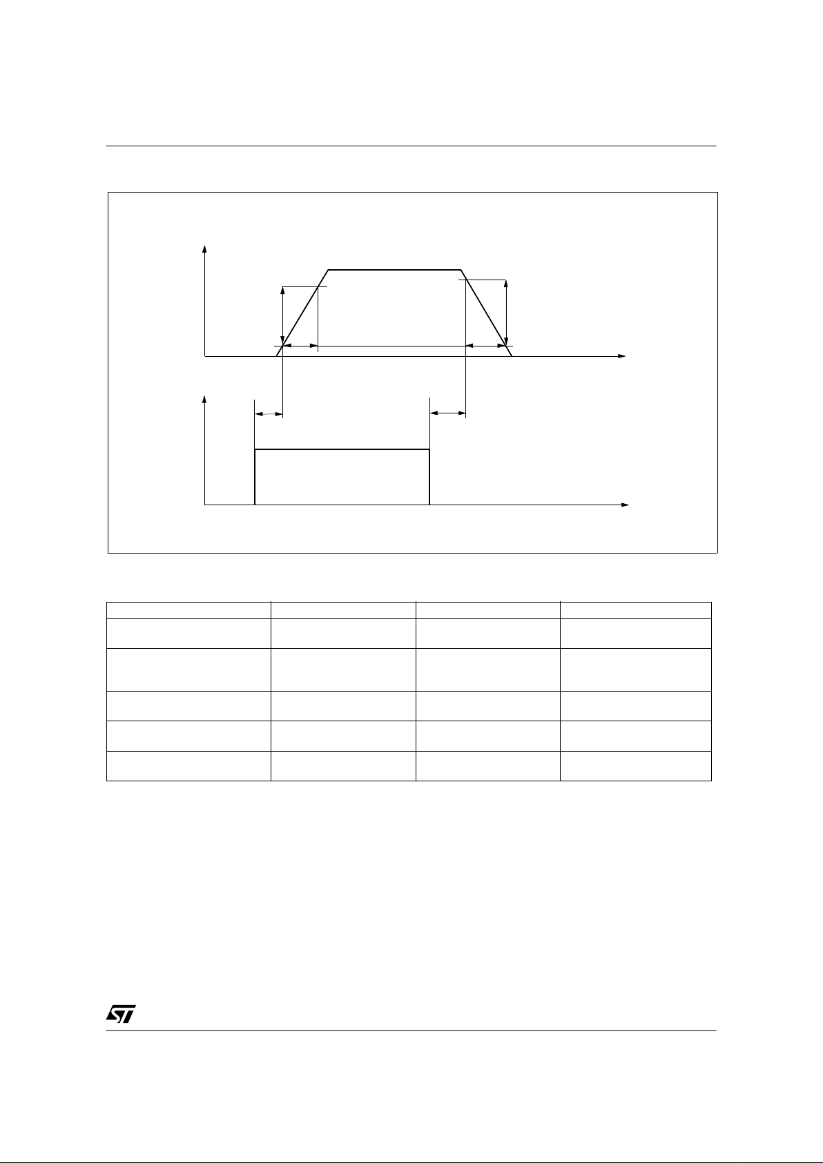
VN800S / VN800PT
V
OUT
dV
OUT
/dt
(on)
t
r
80%
10%
t
f
dV
OUT
/dt
(off)
t
d(off)
t
d(on)
V
IN
t
t
90%
Switching time Waveforms
TRUTH TABLE
CONDITIONS INPUT OUTPUT STATUS
Normal Operation
L
H
L
H
H
H
Current Limitation
L
H
H
L
X
X
H
(T
j
< T
TSD
) H
(T
j
> T
TSD
) L
Overtemperature
L
H
L
L
H
L
Undervoltage
L
H
L
L
X
X
Overvoltage
L
H
L
L
H
H
6/21
VN800S / VN800PT
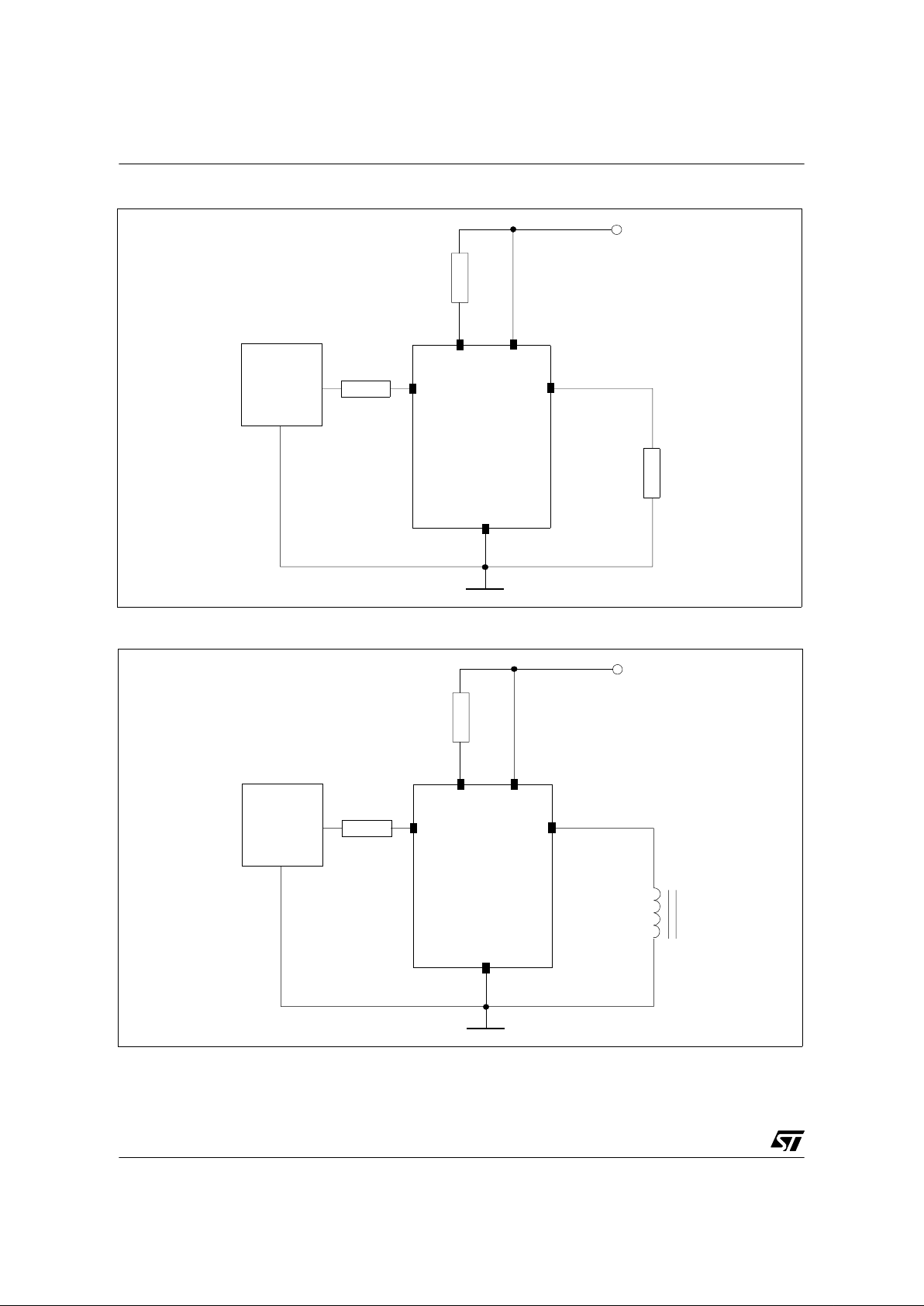
Figur e 1: Peak Short Circuit Current Test Circuit
Figur e 2: Avalanche Energy Test Circuit
10kΩ
CONTROL
UNIT
R
IN
INPUT
GND
OUTPUT
R
L
=10mΩ
+V
CC
GND
STATUS
10kΩ
CONTROL
UNIT
R
IN
INPUT
GND
OUTPUT
LOAD
+V
CC
GND
STATUS
V
CC
V
CC
7/21
VN800S / VN800PT
GND PROTECTION NETWORK AGAINST
REVERSE BATTERY
Soluti on 1: Resistor in the ground line (R
GND
only). This
can be us ed with any t ype of load .
The fo llow ing is an indica tion on how to di mension the
R
GND
resistor.
1) R
GND
≤ 600mV / (I
S(on)ma x
).
2) R
GND
≥ (−VCC) / (-I
GND
)
where -I
GND
is the DC re vers e grou nd pi n cu rren t an d can
be found in the absolute maximum rating section of the
device’s datasheet.
Power Dissipation in R
GND
(when VCC<0: during reverse
battery situations) is:
P
D
= (-VCC)2/R
GND
This resistor can be shared amongst several different
HSD. Please note tha t t h e va l u e of this resis t o r sh ould be
calcul ated with form ula (1) wher e I
S(on)max
becomes t he
sum of the maximum on-state currents of the different
devices.
Please note that if the microprocessor ground is not
common with the device ground then the R
GND
will
produce a shift (I
S(on)max
* R
GND
) in the input thresholds
and the status output values. This shift will vary
depending on many devices are ON in the case of several
high side drivers sharing the same R
GND
.
If the calculated power dissipation leads to a large resistor
or several devices hav e to share the sa me resisto r then
the ST suggests to utiliz e Solu tio n 2 (se e below ).
Solution 2:
A diode (D
GND
) in the gro und line.
A resistor (R
GND
=1kΩ) should be inserted in parallel to
D
GND
if the devi ce will be driving an inducti ve load.
This small signal diode can be safely shared amongst
several different HSD. Also in this case, the presence of
the ground network wi ll produce a shift (
j
600mV) in t he
input threshold and the status output values if the
microprocessor ground is not common with the device
ground. This shift will not vary if more than one HSD
shares the same diode/resistor net work.
µC I/Os PROTECTION:
If a ground protection network is used and negative
transients are present on the V
CC
line, th e con trol p ins will
be pulled negative. ST suggests to insert a resistor (R
prot
)
in lin e to prevent the µC I/Os pins to latch-up.
The value of these resistors is a compromise between the
leakage c urrent of µC an d the current required by the
HSD I/Os ( Input le vels comp atibilit y) wi th the lat ch-up li mit
of µC I/Os.
-V
CCpeak/Ilatchup
≤ R
prot
≤ (V
OHµC-VIH-VGND
) / I
IHmax
Calculation example:
For V
CCpeak
= - 100V an d I
latchup
≥ 20mA; V
OHµC
≥ 4.5V
5kΩ ≤ R
prot
≤ 65kΩ.
Recommended R
prot
value is 10kΩ.
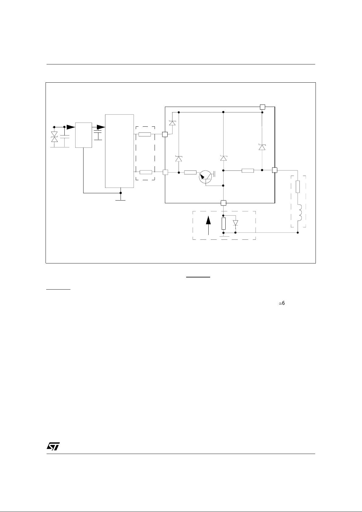
APPLICATION SCHEMATIC
V
CC
INPUTn
GND
STATUSn
OUTPUTn
Volt.
Reg
BUS
ASIC
Control & Diagnostic I/O
5V
24VDC
V
CC
DGND
VGND
RGND
Rprot
Rprot
LOAD
R
L
 Loading...