SGS Thomson Microelectronics VN800PT-8961, VN800S-8961 Datasheet

®
July 2002 1/22
VN800S(8 961 )
/ VN800P T( 8 961 )
HIGH SIDE DRIVER
■ CMOS COMPATIBLE INPUT
■ THERMAL SHUTDOWN
■ CURRENT LIMITATION
■ SHORTED LOAD PROTECTION
■ UNDERVOLTAGE AND OVERVOLTAGE
SHUTDOWN
■ PROTECTION AGAINST LOSS OF GROUND
■ VERY LOW STAND-BY CURRENT
■ REVERSE BATTERY PROTECTION (*)
DESCRIPTION
The VN800S(8961), VN800PT(8961) are
monolithic devices made by using
STMicroelectronics VIPower M0-3 Technology,
intended for driving any kind of load with one side
connected to ground.
Active VCC pin voltage clamp protec ts the device
against low energy spikes (see ISO7637 transient
compatibility table). Active current limitation
combined with thermal shutdown a nd automatic
restart protect the device against overload.
Device autom atically turns off in case of g round
pin disconnection.
TYPE R
DS(on)
I
OUT
V
CC
VN800S(8961)
VN800PT(8961)
135 mΩ 1.2 A 36 V
SO-8
PPAK
ORDER CODES
PACKAGE TUBE T&R
SO-8 VN800S(8961) VN800S(8961)TR
PPAK VN800PT(8961) VN800PT(8961)TR
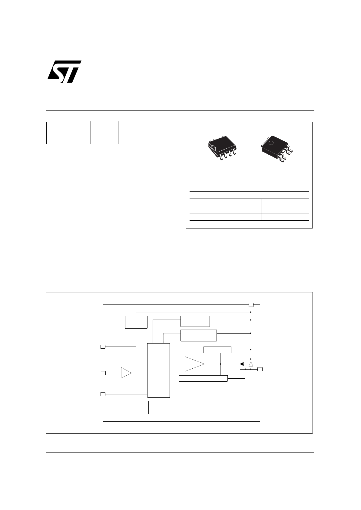
BLOCK DIAGRAM
UNDERVOLTAGE
OVERTEMPERATURE
GND
INPUT
OUTPUT
OVERVOLTAGE
CURRENT LIMITER
LOGIC
DRIVER
Power CLAMP
STATUS
V
CC
CLAMP
DETECTION
DETECTION
DETECTION
(*) See note at page 8
V
CC

2/22
VN800S(8961) / VN800PT(8961)
ABSOLUTE MAXIMUM RATI NG
CONNECTION DIAGRAM (TOP VIEW)
CURRENT AND VOLTAGE CONVENTIONS
Symbol Parameter
Value
Unit
SO-8 PPAK
V
CC
DC Supply Voltage 41 V
- V
CC
Reverse DC Supply Voltage - 0.3 V
- I
GND
DC Reverse Ground Pin Curren t - 200 mA
I
OUT
DC Output Current Internally Limited A
- I
OUT
Reverse DC Output Current - 6 A
I
IN
DC Input Curre nt +/- 10 mA
V
IN
Input Vol t age Range -3/+V
CC
V
V
STAT
DC Status Vol tage + V
CC
V
V
ESD
Electrostatic Discharge (Human Body Model: R=1.5KΩ; C=100pF)
- INPU T
- STATUS
- OUTPU T
- V
CC
4000
4000
5000
5000
V
V
V
V
E
MAX
Maximum Switching Energy
(L=77.5mH; R
L
=0Ω; V
bat
=13.5V ; T
jstart
=150ºC ; IL=1.5A)
121 mJ
E
MAX
Maximum Switching Energy
(L=125mH; R
L
=0Ω; V
bat
=13.5V; T
jstart
=150ºC; IL=1.5A)
195 mJ
P
tot
Powe r Dissip at ion TC=25°C 4.2 41.7 W
T
j
Junction Operating Temperature Internally Limited °C
T
c
Case Operating Tempe rature - 40 to 150 °C
T
stg
Storage Temperature - 55 to 150 °C
L
max
Max Induc ti ve Load (VCC=30V; R
LOAD
=48Ω; T
amb
=100°C;
Rth
case>ambient
≤25°C/W)
2H
V
CC
V
CC
OUTPUT
OUTPUT
N.C.
GND
STATUS
INPU T
1
4
5
8
5
4
3
2
1
STATUS
OUTPUT
GND
INPUT
V
CC
SO-8 PPAK
INPUT
I
S
I
IN
V
IN
V
CC
STATUS
I
STAT
V
STAT
GND
V
CC
I
OUT
V
OUT
I
GND
OUTPUT

3/22
VN800S(8961) / VN800PT(8961)
THERMAL DATA
(*) When mounted on FR4 printed circuit board with 0.5 cm2 of copper area ( at least 35µ thick) connected to all VCC pins.
(**) When mounted on FR4 printed circuit board with 0.5 cm
2
of copper area ( at least 35µ thick).
ELECTRICAL CHARACTERISTICS (8V<VCC<36V; -40°C<Tj<150°C, unless otherwise specified)
POWER
SWITCHING (VCC=24V)
INPUT PIN
Symbol Parameter
Value
Unit
SO-8 PPAK
R
thj-case
Thermal R esistance Junctio n-case
Max
-3°C/W
R
thj-lead
Thermal R esistance Junctio n-lead
Max
30 - °C/W
R
thj-amb
Thermal R esistance Junctio n-ambient
Max
93 (*) 78 (**) °C/W
Symbol Parameter Test Conditions Min Typ Max Unit
V
CC
Operating Supply Voltage 5.5 36 V
V
USD
Undervolt age Shut- down 3 4 5.5 V
V
OV
Overvolt age Shut-d own 36 V
R
ON
On State Resistance
I
OUT
=0.5A; Tj=25°C
I
OUT
=0.5A
135
270
mΩ
mΩ
I
S
Supply Current
Off State; V
CC
=24V; T
case
=25°C
On State; V
CC
=24V
On State; V
CC
=24V; T
case
=100°C
10
1.5
20
3.5
2.6
µA
mA
mA
I
LGND
Output Current at turn-off
V
CC=VSTAT=VIN=VGND
=24V
V
OUT
=0V
1mA
I
L(off1)
Off State Output Curr ent VIN=V
OUT
=0V 0 50 µA
I
L(off2)
Off State Output Curr ent VIN=V
OUT
=0V; Vcc=13V; Tj =125°C 5 µA
I
L(off3)
Off State Output Curr ent VIN=V
OUT
=0V; Vcc=13V; Tj =25°C 3 µA
Symbol Parameter Test Conditions Min Typ Max Unit
t
d(on)
Turn-on Delay Time
RL=48Ω from VIN rising edge to
V
OUT
=2.4V
10 µs
t
d(off)
Turn-off Delay Tim e
RL=48Ω from VIN falli ng edge to
V
OUT
=21.6V
40 µs
dV
OUT
/
dt
(on)
Turn-on Voltage Slo pe
RL=48Ω from V
OUT
=2.4V to
V
OUT
=19.2V
See
relativ e
diagram
V/µs
dV
OUT
/
dt
(off)
Turn-off Voltage S lope
RL=48Ω from V
OUT
=21.6V to
V
OUT
=2.4V
See
relative
diagram
V/µs
Symbol Par am eter Test Co nditions Min Typ Max Unit
V
INL
Input Low Level 1.25 V
I
INL
Low Leve l Input Curr ent VIN=1.25V 1 µA
V
INH
Input High Level 3.25 V
I
INH
High Level Input Current VIN=3.25V 10 µA
V
I(hyst)
Input Hysteresis Voltage 0.5 V
I
IN
Input Current VIN=VCC=36V 200 µA
1

4/22
VN800S(8961) / VN800PT(8961)
2
ELECTRICAL CHARACTERISTICS (continued)
STATUS PIN
PROTECTIONS
Symbol Parameter Test Conditions Min Typ Max Unit
V
STAT
Status Low Output Voltage I
STAT
=1.6 mA 0.5 V
I
LSTAT
Status Leakage Current Normal Operation; V
STAT=VCC
=36 V 10 µA
C
STAT
Status Pin Input
Capacitance
Normal Operation; V
STAT
= 5V 30 pF
Symbol Parame ter Test Conditions Min Typ Max Unit
T
TSD
Shut-down Temperature 150 175 200 °C
T
R
Reset Temp erature 135 °C
T
hyst
Ther ma l Hy steresis 7 15 °C
T
SDL
Status Delay in Overload
Condition
T
j>Tjsh
20 µs
I
lim
DC Short Circuit Current VCC=16V; R
LOAD
=10mΩ 1.2 2 A
V
demag
Turn-off Output Clamp
Voltage
I
OUT
=0.5 A; L=6mH VCC-47 VCC-52 VCC-57 V
OVERTEMP STATUS TIMING
Tj>T
jsh
V
IN
V
STAT
t
SDL
t
SDL

5/22
VN800S(8961) / VN800PT(8961)
V
OUT
dV
OUT
/dt
(on)
t
r
80%
10%
t
f
dV
OUT
/dt
(off)
t
d(off)
t
d(on)
V
IN
t
t
90%
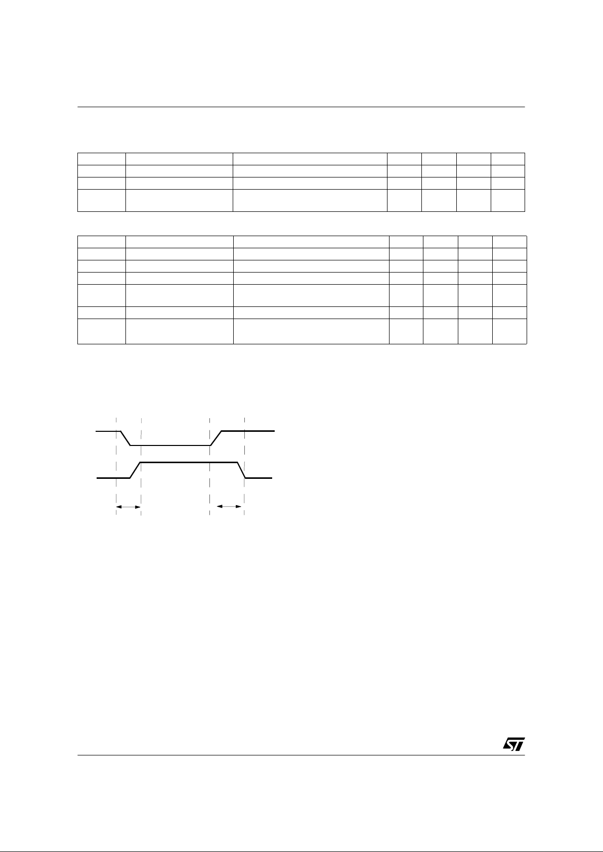
Switching time Waveforms
TRUTH TABLE
CONDITIONS INPUT OUTPUT STATUS
Normal Operation
L
H
L
H
H
H
Current Limitation
L
H
H
L
X
X
H
(T
j
< T
TSD
) H
(T
j
> T
TSD
) L
Overtemperature
L
H
L
L
H
L
Undervoltage
L
H
L
L
X
X
Overvoltage
L
H
L
L
H
H

6/22
VN800S(8961) / VN800PT(8961)
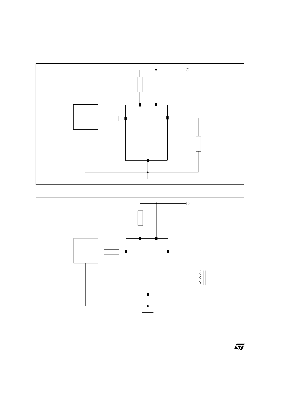
Figur e 1: Peak Short Circuit Current Test Circuit
Figur e 2: Avalanche Energy Test Circuit
10kΩ
CONTROL
UNIT
R
IN
INPUT
GND
OUTPUT
R
L
=10mΩ
+V
CC
GND
STATUS
10kΩ
CONTROL
UNIT
R
IN
INPUT
GND
OUTPUT
LOAD
+V
CC
GND
STATUS
V
CC
V
CC

7/22
VN800S(8961) / VN800PT(8961)
ISO T/R 7637/1
Test Pulse
TEST LEVELS
I II III IV
Delays and
Impedance
1 -25 V -50 V -75 V -100 V 2 ms 10 Ω
2 +25 V +50 V +75 V +100 V 0.2 ms 10 Ω
3a -25 V -50 V -100 V -150 V 0.1 µs 50 Ω
3b +25 V +50 V +75 V +100 V 0.1 µs 50 Ω
4 -4 V -5 V -6 V -7 V 100 ms, 0.01
Ω
5 +26.5 V +46.5 V +66.5 V +86.5 V 400 ms, 2
Ω
ISO T/R 7637/1
Test Pulse
TEST LEVEL S RESULTS
IIIIIIIV
1CCCC
2CCCC
3aCCCC
3bCCCC
4CCCC
5CEEE
ELECTRICAL TRANSIENT REQUIREMENTS ON VCC PIN
CLASS CONTENTS
C All functions of the device are performed as designed after exposure to disturbance.
E One or more functions of the device is not performed as designed aft er exposure to dist urbance
and canno t be returned to proper operation without replacing the device.
 Loading...