

SGS Thomson Microelectronics VN772K Datasheet
®
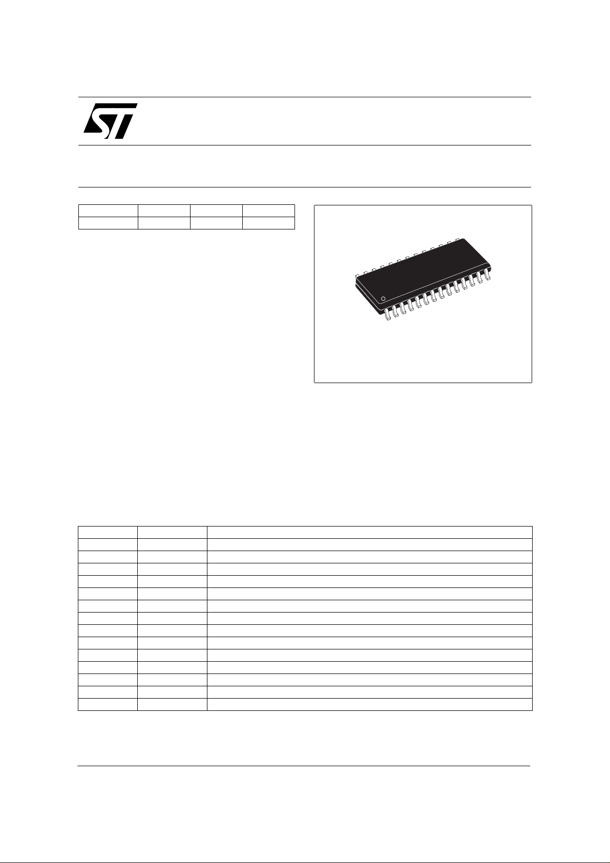
VN772K
QUAD SM ART P OWE R SOL ID STATE RE LAY
FOR COMP LET E H B RIDG E CO NF IGUR ATIONS
TYPE R
VN772K 120 mΩ (*) 9A (**) 36V
(*) Total resis tance of one side in bridge configuration
(**) Typica l c ur r ent limitation value
■ SUITED AS LOW VOLTAGE BRIDGE
■ LINEAR CURRENT LIMITATION
■ VERY LOW STAND-BY POWER DISSIPATION
■ SHORT CIRCUIT PROTECTED
■ DOUBLE STATUS FLAG DIAGNOSTIC (OPEN
DS(on)
I
OUT
V
CC
DRAIN)
■ INTEGRATED CLAMPING CIRCUITS
■ UNDERVOLTAGE PROTE CTIO N
■ ESD PROTECTION
DESCRIPTION
The VN772K is a device formed by three
monolithic chips housed in a standard SO-28
package: a double high side and two low side
switches. Both the d ouble high si de an d low side
switches are made using |STMicroelectronics
VIPower™ M0-3 Technology. This device is
suitable to drive a DC motor in a bridge
configuration as well as to be used as a quad
switch for any low voltage application. The dual
SO-28
high side switches have bui lt-i n ther mal s hutdo wn
to protect the chips from overtemperature and
current limiter blocks to protect the device from
short circuit. Statu s output is provi ded to indicate
open load in off and on state and overtemperature.
The low sid e swi tches are two O MNIFET II typ es
(fully autopr otecte d Powe r MOSF ET in V IPower™
technology). They have built-in thermal shutdown,
linear current limitation and overvoltage clamping.
Fault feedback for thermal intervention can be
detected by monitoring the voltage at the input pin.
PIN FUNCTION
No NAME FUNCTION
1, 3, 25, 28 DRAIN 3 Drain of Switch 3 (low-side switch)
2 INPUT 3 Input of Switch 3 (low-side switch)
4, 11 N.C. Not Connected
5, 10, 19, 24 V
6 GND Ground of Switches 1 and 2 (high-side switche s)
7 INPUT 1 Input of Switch 1 (high-side swi tches)
8 DIAGNOSTIC Diagn ostic of Sw itches 1 and 2 (high-side swit ches)
9 INPUT 2 Input of Switch 2 (high-side swi tch)
12, 14, 15, 18 DRAIN 4 Drain of switch 4 (low-side switch)
13 INPUT 4 Input of Switch 4 (low-side switch)
16, 17 SOURCE 4 Source of Switch 4 (l ow-side switch)
20, 21 SOURCE 2 Source of Switch 2 (hi gh-side switch)
22, 23 SOURCE 1 Source of Switch 1 (hi gh-side switch)
26, 27 SOURCE 3 Source of Switch 3 (l ow-side switch)
November 2002 1/21
CC
Drain of Switches 1 and 2 (high-side switches) and Power Supply Voltage
1
VN772K
BLO C K DIAG RA M
V
cc
CLAMP
OVERVOLTAGE
UNDERVOLTAGE
V
cc
GND
INPUT1
DIAG
INPUT2
INPUT3
OVERTEMP. 1
OVERTEMP. 2
LOGIC
CLAMP 1
DRIVER 1
CURRENT LIMITER 1
OPENLOAD ON 1
OPENLOAD OFF 1
Gate
Control
Over
T emperature
DRIVER 2
CURRENT LIMITER 2
OPENLOAD ON 2
OPENLOAD O FF 2
Overvoltage
Clamp
Linear
Current
Limiter
SOURCE1
CLAMP 2
SOURCE2
DRAIN3
SOURCE3
2/21
1
INPUT4
Gate
Control
Over
T emperature
Overvoltage
Clamp
Linear
Current
Limiter
DRAIN4
SOURCE4
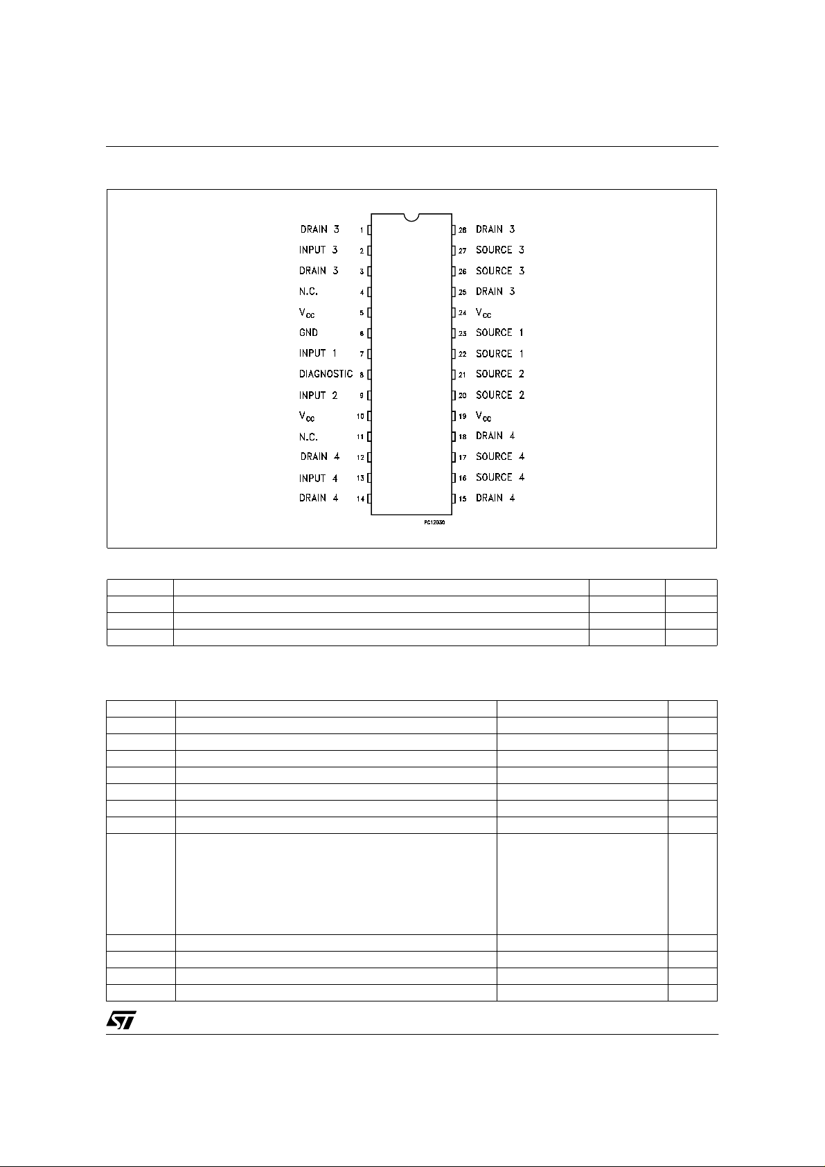
CONNECTION DIAGRAM
VN772K
THERMAL DATA
Symbol Parameter Value Unit
R
thj-case
R
thj-case
R
thj-amb
Thermal Resist ance Junction-case (High-side switch) MAX 20 °C/W
Thermal Resist ance Junction-case (Low-side switch) MAX 20 °C/W
Thermal Resist ance Junction-ambient MAX 60 °C/W
ABSOLUTE MAXIMUM RATI NG
DUAL HIGH SIDE SWITCH
Symbol Parameter Value Unit
tot
DC Supply Voltage 41 V
Reverse DC Supply Voltage - 0.3 V
CC
DC Reverse Ground Pin Current - 200 mA
DC Output Current Internally Limited A
Reverse DC Output Current - 6 A
DC Input Current +/- 10 mA
DC Status Cur rent +/- 10 mA
Electrostatic Discharge (Human Body Model: R=1.5KΩ;
C=100pF)
- INPUT
- STATUS
- OUTPU T
- V
CC
4000
4000
5000
5000
Powe r Dissipation Tc=25°C 6 W
Junction Operating Temperature Internally Limited °C
j
Case Operating Temperature - 40 to 150 °C
c
Storage Temperature - 55 to 150 °C
V
- V
- I
I
OUT
- I
I
STAT
V
P
T
CC
GND
OUT
I
IN
ESD
T
T
stg
V
V
V
V
3/21
1
VN772K
ABSOLUTE MAXIMUM RATING (continued)
LOW SIDE SWITCHES
Symbol Parameter Value Unit
V
DS
V
IN
I
IN
R
IN MIN
I
D
I
R
V
ESD1
V
ESD2
P
tot
T
j
ELECTRICAL CHARACTERISTICS FOR DUAL HIGH SIDE SWITCH
(8V<VCC<36V; -40°C< Tj <150°C, unless otherwise specified)
POWER OUTPUTS (Per each channel)
Symbol Parameter Test Conditions Min Typ Max Unit
(**) Operating Supply Voltag e 5.5 13 36 V
V
CC
(**) Undervol tage Shut -down 3 4 5.5 V
V
USD
(**) Overv olt age Shut-d ow n 36 V
V
OV
R
DS(on)
(**) Supply Current
I
S
I
L(off1)
I
L(off2)
I
L(off3)
I
L(off4)
Drain-source Voltage (VIN=0V) Internally Clampe d V
Input Voltage Internally Clamped V
Input Current +/-20 mA
Minim um Input Series Impe dance 150 Ω
Drain Current Inte rnally Lim ited A
Reverse DC Output Current -10.5 A
Electrostat ic Dischar ge (R=1.5KΩ , C=100pF) 4000 V
Electrostat ic Dischar ge on output pin only
(R=330Ω, C=150pF)
16500 V
Power Dissipation (TC=25°C) 6 W
Opera ting Junct ion Temperature Internally limited °C
I
=2A; Tj=25°C
On State Resistance
OUT
I
=2A; VCC>8V
OUT
Off Stat e; V
Off Stat e; V
V
IN=VOUT
On State; V
Off State Output Current VIN=V
OUT
Off State Output Current VIN=0V; V
Off State Output Current VIN=V
Off State Output Current VIN=V
OUT
OUT
=13V; V
CC
=13V; Tj =25°C;
CC
=0V
=13V
CC
IN=VOUT
=0V
12
12
5
=0V; VCC=36V; Tj=125°C 0 50 µA
=3.5V -75 0 µA
OUT
=0V; VCC=13V; Tj =125°C 5 µA
=0V; VCC=13V; Tj =25°C 3 µA
60
120
40
25
7
mΩ
mΩ
µA
µA
mA
SWITCHING (Per each channel) (VCC=13V)
Symbol Parameter Test Condit ions Min Typ Max U nit
t
d(on)
t
d(off)
dV
OUT
dt
(on)
dV
OUT
dt
(off)
(**) Per device
4/21
Turn-on Delay Time
Turn-off Delay Time
/
Turn-on Voltage Slope
/
Turn-off Voltage Slope
RL=6.5Ω from VIN rising edge to
V
=1.3V
OUT
RL=6.5Ω from VIN falling edge to
V
=11.7V
OUT
RL=6.5Ω from V
=10.4V
V
OUT
RL=6.5Ω from V
V
=1.3V
OUT
=1.3V to
OUT
=11.7V to
OUT
30 µs
30 µs
See
relative
diagram
See
relative
diagram
V/µs
V/µs
VN772K
ELECTRICAL CHARACTERISTICS FOR DUAL HI GH SIDE SWITCH (continued)
INPUT PINS (Per each channel)
Symbol Parameter Test Conditions Min Typ Max Unit
V
I
V
I
IH
V
I(hyst)
V
ICL
LOGIC INPUT (Per each channel)
Symbol Parameter Test Conditions Min Typ Max Unit
V
I
V
I
IH
V
I(hyst)
V
ICL
STATUS PIN (Per each channel)
Symbol Parameter Test Conditions Min Typ M ax Unit
V
STAT
I
LSTAT
C
STAT
V
SCL
Input Low Level 1.25 V
IL
Low Level Input Current VIN=1.25V 1 µA
IL
Input High Level 3.25 V
IH
High Level Input Current VIN=3.25V 10 µA
Input Hyst eresis Vo lt age 0.5 V
=1mA
I
Input Clamp Voltage
Input Low Level 1.25 V
IL
Low Level Input Current VIN = 1.25V 1 µA
IL
Input High Level 3.25 V
IH
IN
I
= -1mA
IN
6.5 7.4
-0.7
High Level Input Current VIN = 3.25V 10 µA
Input Hyst eresis Vo lt age 0.5 V
= 1mA
I
Input Clamp Voltage
Status Low Output Voltage I
IN
I
= -1mA
IN
= 1.6 mA 0.5 V
STAT
Status Leakage Current Normal Operation; V
Status Pin Input
Capacitance
Status Clamp Voltage
Normal Operation; V
= 1mA
I
STAT
I
= - 1mA
STAT
= 5V 10 µA
STAT
= 5V 100 pF
STAT
66.8
-0.7
66.8
-0.7
8.5 V
8V
8V
V
V
V
PROTECTIONS (Per each channel)
Symbol Parameter Test Condit ions M in Typ Max Unit
T
T
t
SDL
I
V
demag
TSD
T
hyst
lim
Shut-down Temperature 150 175 200 °C
Reset Temp erature 135 °C
R
Ther ma l Hy steresi s 7 15 °C
Status Delay in Overload
Conditions
Current limitation T
Tj>T
=125°C
j
TSD
8.5
6
915
5.5V<VCC<36V
Turn-off Output Clamp
Voltage
=2A; L= 6m H VCC-41 VCC-48 VCC-55 V
I
OUT
20 µs
15
15
A
A
A
5/21
1
VN772K
ELECTRICAL CHARACTERISTICS FOR DUAL HI GH SIDE SWITCH (continued)
OPENLOAD DETECTION (Per each channel)
Symbol Parameter Test Conditions Min Typ Max Unit
I
OL
t
DOL(on)
V
T
DOL(off)
Openload ON State
Detectio n Threshol d
Openload ON State
Detection Delay
=5V 50 100 200 mA
V
IN
=0A 200 µs
I
OUT
Openload OFF State
Voltage Detection
OL
Threshold
Openload Detection Delay
at Turn Off
VIN=0V 1.5 2.5 3.5 V
1000 µs
6/21
VN772K
ELECTRICAL CHARACTERISTICS FOR LOW SIDE SWITCHES
(-40°C < Tj < 150°C, unless otherwise specified)
OFF
Symbol Parameter Test Conditions Min Typ Max Unit
V
CLAMP
V
CLTH
V
I
V
I
DSS
INTH
ISS
INCL
Drain-source Clamp
Voltage
Drain-source Clamp
Threshold Voltage
Input Threshold Voltage VDS=VIN; ID=1mA 0.5 2.5 V
Supply Cur rent fro m Inpu t
Pin
Input-Source Clamp
Voltage
Zero Input Voltage Drain
Current (VIN=0V)
ON
Symbol Parameter Test Conditions Min Typ Max Unit
R
DS(on)
Stati c Dr ain-sourc e On
Resist an ce
(Tj=25°C, unless otherwise specified)
DYNAMIC
Symbol Parameter Test Conditions Min Typ Max Unit
Forward
(*)
g
fs
C
OSS
Transconductance
Output Capacitance VDS=13V; f=1MHz; VIN=0V 220 pF
VIN=0V; ID=3.5A 40 45 55 V
VIN=0V; ID=2mA 36 V
VDS=0V; VIN=5V 100 150 µA
=1mA
I
IN
I
=-1mA
IN
=13V; VIN=0V; Tj=25°C
V
DS
V
=25V; VIN=0V
DS
=5V; ID=3.5A; Tj=25°C
V
IN
V
=5V; ID=3.5A
IN
6
-1.0
6.8 8
-0.3
30
75
60
120
VDD=13V; ID=3.5A 9 S
V
µA
mΩ
SWITCHING
Symbol Parameter Test Conditions Min Typ M ax Unit
t
d(on)
t
t
d(off)
t
t
d(on)
t
t
d(off)
t
(dI/dt)
Q
Turn-on Delay Time
Rise Time 470 1500 ns
r
Turn-off Delay Time 500 1500 ns
Fall Time 350 1000 ns
f
VDD=15V; ID=3.5A
V
=5V; R
gen
gen=RIN MIN
=150Ω
Turn-on Delay Time
Rise Time 4.6 14.0 µs
r
Turn-off Dela y Tim e 5.4 16.0 µs
Fall Ti me 3.6 11.0 µs
f
Turn-on Current Slope
on
Total In put Charge
i
VDD=15V; ID=3.5A
V
=5V; R
gen
=15V; ID=3.5A
V
DD
V
=5V; R
gen
=12V; ID=3.5A; VIN=5V
V
DD
I
=2.13mA
gen
=2.2KΩ
gen
gen=RIN MIN
=150Ω
100 300 ns
0.75 2.3 µs
6.5 A/µs
18 nC
SOURCE DRAIN DIODE
Symbol Parameter Tes t Conditions Min Typ Max Unit
(*) Forward On Voltage ISD=3.5A; VIN=0V 0.8 V
V
SD
Q
I
RRM
t
Reverse Recovery Time
rr
Reverse Recovery Charge 0.28 µC
rr
Reverse Re covery C urrent 2.5 A
=3.5A; dI/dt=20A/µs
I
SD
V
=30V; L= 20 0 µ H
DD
220 ns
7/21
 Loading...