

SGS Thomson Microelectronics VN771 Datasheet
VN771
QUAD SMART POWER SOLID STATE RELAY
FOR COMPLETE H-BRIDGE CONFIGURATIONS
TYPE R
VN77 1 0.140 Ω 14 A 26 V
* Total resistance of one side in bridge configuration
■ IDEAL AS A LOW VOLTAGEBRIDGE
■ VERYLOW STAND-BYPOWER
*I
DS(on)
OUT
V
CC
DISSIPATION
■ OVER-CURRENTPROTECTED
■ STATUSFLAG DIAGNOSTICSON UPPER
SIDE
■ OPENDRAIN DIAGNOSTICS OUTPUT
■ UNDER-VOLTAGEPROTECTION
■ SUITABLEAS QUADSWITCH
DESCRIPTION
The VN771 is a device formed by three
monolithic chips housed in a standard SO-28
package: a double high side and two Power
MOSFETs. The double high side are made using
STMicroelectronics VIPower technology; Power
MOSFETs are made by using the new advanced
strip lay-out technology This device is suitable to
drive a DC motor in a bridge configurationas well
as to be used as a quad switch for any low
voltage application. The dual high side switches
have built-in thermal shut-down to protect the
chip from over temperature and short circuit,
status output to provide indication for open load
in off and on state, overtemperature conditions
and stuck-onto V
CC
.
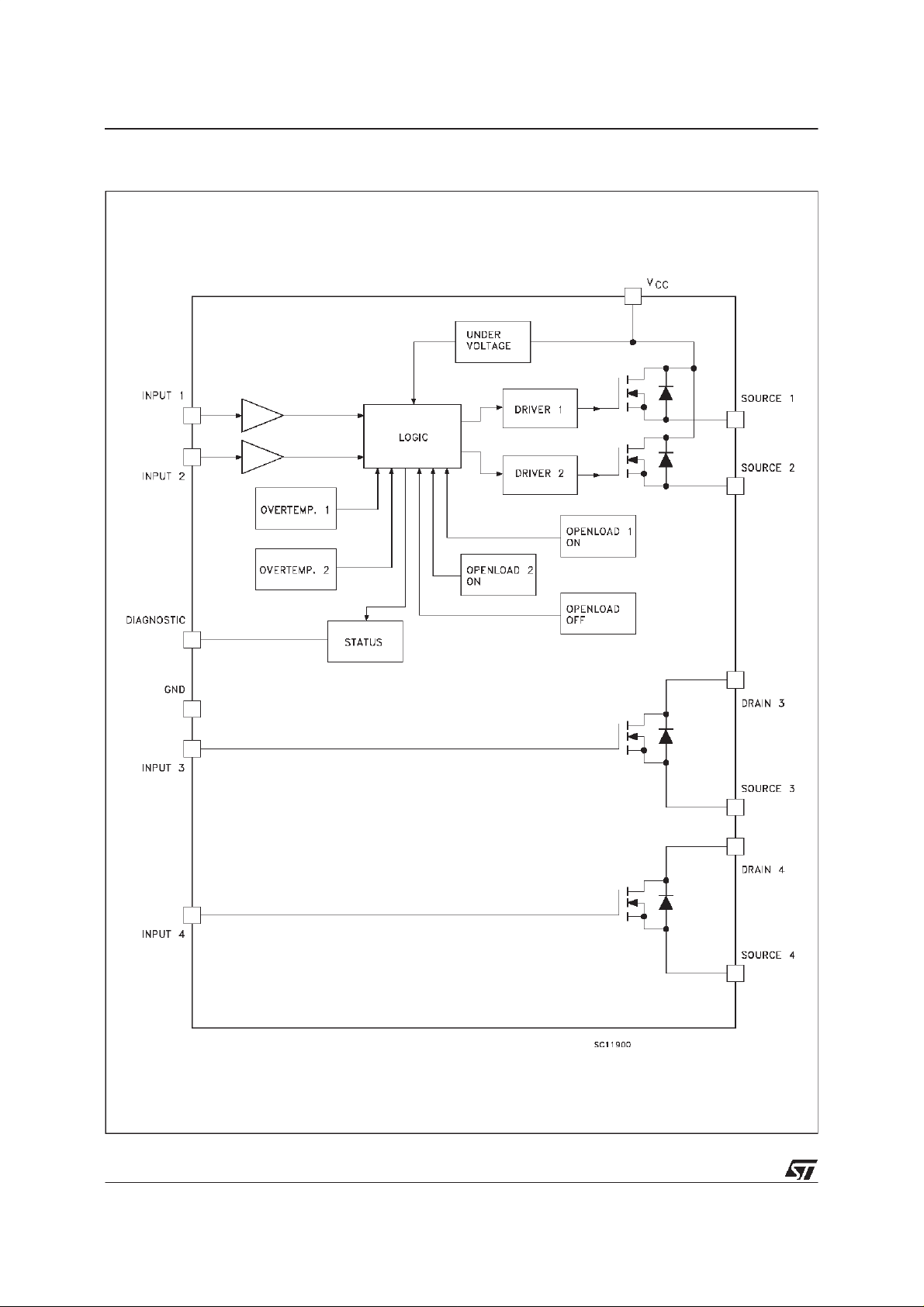
DUALHIGH-SIDESWITCH
From the falling edge of the input signal, the
status output, initially low to signal a fault
condition (overtemperature or open load
on-state), will go back to a high state with a
different delay in case of overtemperature (tpovl)
and in case of open open load (
) respectively.
tpol
This feature allows to discriminate the nature of
the detected fault. To protect the device against
short circuit and over current condition, the
thermal protection turns the integrated Power
SO-28
MOS off at a minimum junction temperature of
o
C. When this temperature returns to 125oC
140
the switch is automatically turned on again. In
short circuit the protection reacts with virtually no
delay, the sensor (one for each channel) being
locatedinside each of the two Power MOS areas.
This positioning allows the device to operate with
one channel in automatic thermal cycling and the
other one on a normal load. An internal function
of the devices ensures the fast demagnetization
of inductive loads with a typical voltage (V
demag
of -18V. This function allows to greatly reduces
the power dissipationaccordingto the formula:
P
dem
=0.5• L
load
• (I
load
)2• [(VCC+V
demag
)/V
demag
] • f
wheref = switching frequencyand
V
= demagnetizationvoltage.
demag
In this device if the GND pin is disconnected,with
V
not exceeding 16V, both channel will switch
CC
off.
PowerMOSFETs
During normal operation, the Input pin is
electrically connected to the gate of the internal
power MOSFET. The devices can be used as a
switchfrom DC to very high frequency.
)
October 1998
1/10
VN771
BLOCK DIAGRAM
2/10
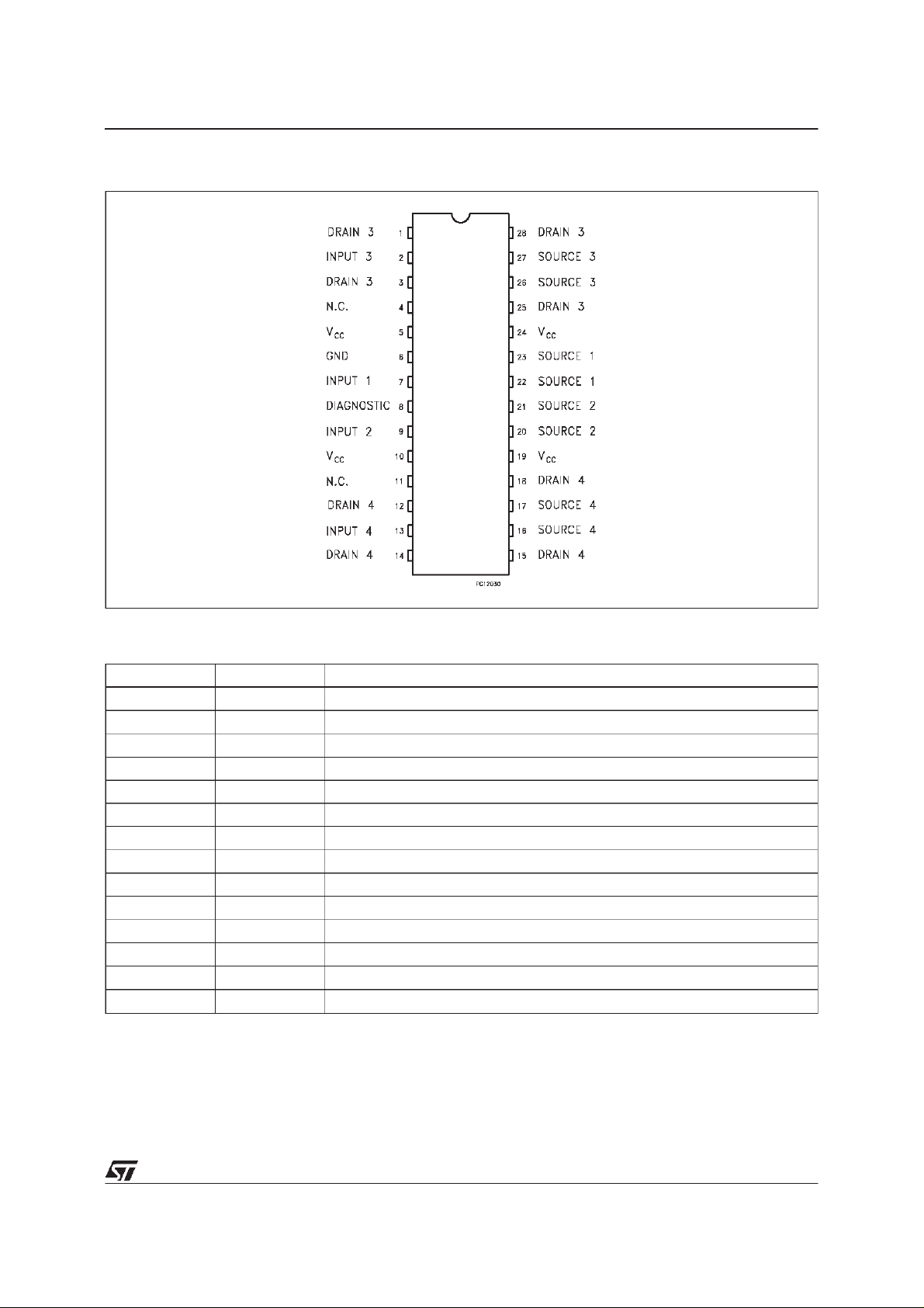
CONNECTION DIAGRAM
VN771
PIN FUNCTION
No NAME FUNCTI O N
1, 3, 2 5 , 28 DRAI N 3 Drain of Switch 3 ( low-sid e switc h )
2 INPUT 3 Input o f Swit ch 3 (l ow-side s wit ch)
4, 11 N.C. Not Con nected
5, 10, 19, 24 V
6 GND Ground of Swit c h es 1 and 2 (h igh - si de swit ches )
7 IN PUT 1 Input of S witch 1 (h igh- s ide sw it ch)
8 DIAGNOSTIC Diagnostic of Switches 1 and 2 (high-side switches)
9 IN PUT 2 Input of S witch 2 (h igh- s ide sw it ch)
12, 14, 15, 1 8 DRAIN 4 Drain of Switch 4 ( low-sid e switc h )
13 INPUT 4 Input o f Swit ch 4 (l ow-side s wit ch)
16, 17 SOURCE 4 Source of Switch 4 (low-side switch)
20, 21 SOURCE 2 Source of Switch 2 (high-side swi tch )
22, 23 SOURCE 1 Source of Switch 1 (high-side swi tch )
26, 27 SOURCE 3 Source of Switch 3 (low-side switch)
CC
Drain of Switches 1a nd 2 ( h igh-side sw itches) and Pow er S upply V olt age
3/10
 Loading...