

SGS Thomson Microelectronics VN710SP Datasheet
®
AUTOMOTIVE GLOW PLUG DRIVER
TYPE R
DS(on)
VN710SP 18mΩ 35 A 16 V
■ CMOS COMPATIBLE INPUT
■ ON STATE OPEN LOAD DETECTION
■ OFF STATE OPENLOAD DETECTION
■ SHORTED LOAD PROTECTION
■ UNDERVOLTAGE AND OVERVOLTAGE
SHUTDOWN
■ PROTECTION AGAINST LOSS OF GROUND
■ VERY LOW STAND-BY CURRENT WHEN
ENABLE PIN IS LOW
■ REVERSE BATTERY PROTECTION (*)
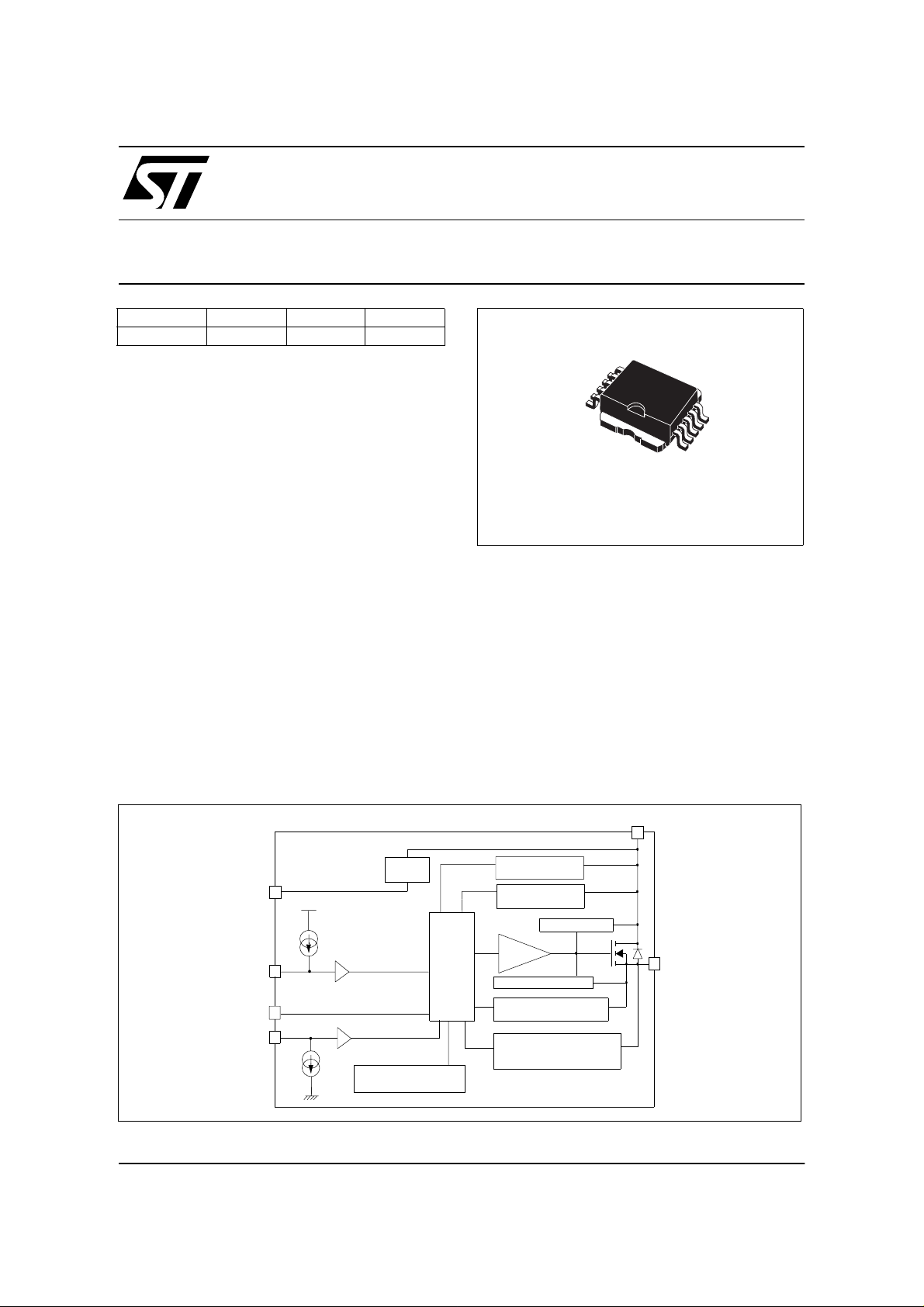
DESCRIPTION
The VN710SP is a mono lithic device m ade using
STMicroelectronics VIPower M0-3 technology,
intended for driving any kind of load with one side
connected to ground. Active VCC pin voltage
clamp protects the device against low energy
spikes (see ISO7637 transients compatibility
table). Active current limitation combined with
thermal shutdown protect the device against
I
OUT
V
CC
VN710S P
PRELIMINARY DATA
10
1
PowerSO-10
overload. Afte r a therma l shutdown eve nt, device
stays latched off and diagnostic stays at a low
level until next falling edge of input signal. The
device detects open load condition both in on
state and off state. Output shorted to VCC is
detected in the off state. Device automatically
turns off in case of ground pin disconnection.
Enable pin allows to switch the device to idle state
with very low quiescent cur rent from VCC. When
enable is low, device tur ns off rega rdless o f input
pin state.
™
BLOCK DIAGRAM
V
CC
V
CC
CLAMP
GND
INPUT
STATUS
ENABLE
(*) See appli c ation schematic at page 7
OVERTEMPERATURE
DETECTION
LOGIC
Octobe r 20 00 1/11
OVERVOLTAGE
DETECTION
UNDERVOLTAGE
DETECTION
Power C LAMP
DRIVER
CURRENT LIMITER
ON STATE OPENLOAD
DETECTION
OFF STATE OPENLOAD
AND OUTPUT SHORTED
TO V
DETECTION
CC
OUTPUT
1
VN710SP
THERMAL DATA
Symbol Parameter Value Unit
R
tj-case
R
tj-amb
(*) When mounted on a standard single-sid ed FR-4 board with 50mm2 of Cu (at least 35µm thick).
ABSOLUTE MAXIMUM RATI NG
Symbol Parameter Value Unit
V
CC
-V
-I
GND
I
OUT
-I
OUT
I
IN
I
en
I
STAT
V
ESD
P
T
T
T
stg
Thermal resistance junction-case 1.4 °C/W
(*) Thermal resistance junction-ambient 52 °C/W
DC supply voltage 41 V
Reverse DC suppl y vo lt a ge -0.3 V
CC
Reverse D C ground pin current -200 mA
DC output current Intern ally limited A
Reverse DC output current -35 A
DC input current +/-10 mA
DC enable current +/-10 mA
DC status current +/-1 0 mA
Electrostatic discharge (R=1.5kΩ; C=100pF) 2000 V
Power dissipation at Tc=25°C89W
tot
Junction operating temperature Internally limited °C
j
Case operating temperature -40 to 150 °C
c
Storage te m perature -55 to 150 °C
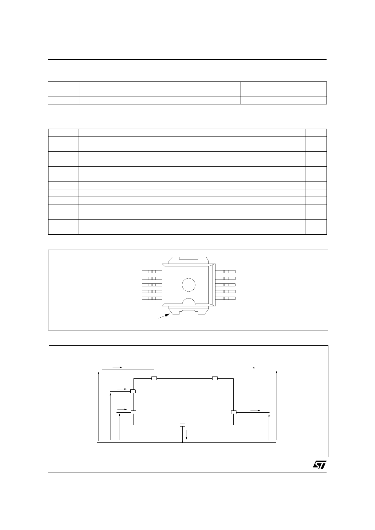
CONNECTION DIAGRAM (TO P VI EW)
GROUND
ENABLE
STATUS
INPUT
N.C.
V
CC
CURRENT AND VOLTAGE CO NVENTIONS
I
en
V
en
I
IN
V
IN
I
STAT
ENABLE
INPUT
STATUS
10
6
7
8
9
11
GND
5
4
3
2
1
V
CC
OUTPUT
OUTPUT
OUTPUT
OUTPUT
OUTPUT
OUTPUT
I
I
OUT
V
CC
OUT
V
CC
2/11
1
V
STAT
I
GND
VN710SP
ELECTRICAL CHARACTERISTICS
(7V<V
<16V; -40°C<Tj<150°C; unless otherwise specified)
CC
POWER
Symbol Parameter Test Conditions Min Typ Max Unit
CC
OV
ON
S
(on)
(off)
Operating supply voltage 5.5 13 16 V
Undervolt age shutdown 345.5V
Overvolt age shutdo wn 16 18 20 V
On state resistance
Supply current
Output current at Turn-off
Off state output current V
Off state output current V
=13V)
CC
Turn-on delay time
Turn-off delay time
/
Turn-on voltage slope
/
Turn-off voltage slope
=15A; Tj=25°C
I
OUT
I
=15A
OUT
Off state; V
=5V
V
IN
Off state; V
VIN=5V; T
On state; VCC=13V; VIN=0V; I
Ven>V
V
CC=VGND
V
IN=Ven
=0V; VIN>V
OUT
=3.5V; VIN>VIH; Ven>V
OUT
enh
=n.c.; V
=13V; Ven=V
CC
=13V; Ven=V
CC
=25°C
j
=16V
OUT
IH
=0V
OUT
OUT
enh
=0V;
=0V;
OUT
RL=0.85Ω, from VIN fallin g edge to
V
=1.3V
OUT
R
=0.85Ω, from VIN rising edge to
L
=11.7V
V
OUT
RL=0.85Ω, from V
V
=10.4V
OUT
RL=0.85Ω, from V
V
=1.3V
OUT
=1.3V to
OUT
=11.7V to
OUT
10
10
=0A;
2.5
050µA
-75 0 µA
40 µs
80 µs
0.1 V/µs
0.1 V/µs
20
40
25
20
4
2mA
V
V
USD
V
R
I
I
LGND
I
L(off1)
I
L(off2)
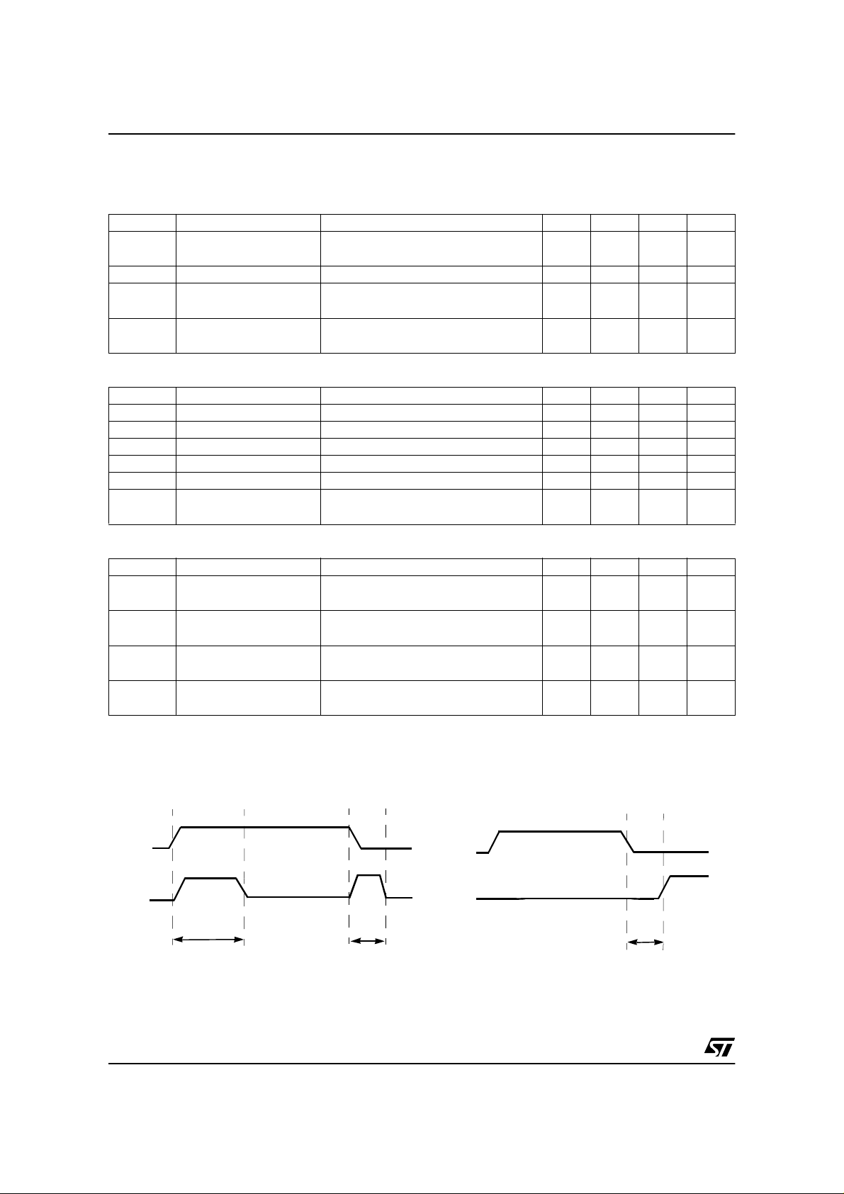
SWITCHING (V
Symbol Parameter Test Conditions Min Typ Max Unit
t
d(on)
t
d(off )
dV
OUT
dt
dV
OUT
dt
mΩ
mΩ
µA
µA
mA
INPUT PIN (active low)
Symbol Parameter Test Conditions Min Typ Max Unit
IL
IL
IH
IH
ICL
Inpu t low level 1.25 V
Low level input current VIN=1.25V ; Ven>V
enh
-35 µA
Inpu t h igh le v el 3.25 V
High level input current
=3.25V ; Ven>V
V
IN
enh
VIN=3.25V ; Ven=0V -300
-4
-4
Input hysteresis voltage 0.5 V
Inpu t clamp voltag e
I
IN
I
IN
=1mA
=-1mA
66.8
-0.7
8V
V
V
V
I
V
I
I(hyst)
ENABLE PIN (active high)
Symbol Parameter Test Conditions Min Typ Max Unit
enl
Enable low level 1.25 V
Low level enable current Ven=1.25V 4 µA
Enable high level 3.25 V
High level enable curre nt Ven=3.25V 35 µA
Enable hysteresis voltage 0.5 V
Enable clamp voltage
I
en
I
en
=1mA
=-1mA
66.8
-0.7
8V
V
V
I
V
I
V
enl
enh
enh
ehyst
encl
1
µA
µA
V
V
3/11
VN710SP
ELECTRICAL CHARACTERISTICS (continued)
STATUS PIN (Open Drain)
Symbol Parameter Test Conditions Min Typ Max Unit
V
STAT
I
LSTAT
C
STAT
V
SCL
Status low output
voltage
Status leakage current Normal operation; V
Status pin input
capacitance
Status clamp voltage
PROTECTIONS
Symbol Parameter Test Conditions Min Typ Max Unit
T
T
t
V
demag
TSD
T
hyst
SDL
I
lim
Shut -do w n t e mp e r at ure 170 190 °C
Reset temperature 135 °C
R
Ther ma l hysteresis 7 15 °C
Overload detection delay Tj>T
Current l imitation 35 55 80 A
Turn-off output clamp
voltage
I
=1.6mA 0.5 V
STAT
=5V 10 µA
STAT
Normal operation; V
=1mA
I
STAT
I
=-1mA
STAT
TSD
I
=2A; VIN=5V; L=6m H VCC-41 VCC-48 VCC-55 V
OUT
=5V 100 pF
STAT
66.8
-0.7
8V
20 µs
V
OPENLOAD DETECTION
Symbol Parameter Test Conditions Min Typ Max Unit
I
OL
Openloa d on state
detection threshold
Openload off state voltage
OL
detection threshold
Openload detection
delay at turn-off
Openload detection
V
t
DOL(off)
t
DOL(on)
delay at turn-on
OPENLOAD STATUS TIMING (with external pull-up)
V
OUT>VOL
V
IN
V
STAT
t
DOL(off)
V
=0V 0.1 1 2 A
IN
VIN=5V 1.5 2.5 3.5 V
500 µs
I
=0V 200 µs
OUT
I
OUT<IOL
t
DOL(on)
V
V
IN
STAT
OVERTEMP STA TUS TIMING
Tj>T
TSD
t
SDL
4/11
2
 Loading...