SINGLE CHANNEL HIGH SIDE SOLID STATE RELAY
TYPE R
VN610SP 10mΩ 45A 36 V
■ OUTPUT CURRENT: 45 A
■ CMOS COMPATIBLE INPUT
■ PROPORTIONAL LOAD CURRENT SENSE
■ UNDERVOLTAGE AND OVERVOLTAGEn
DS(on)
SHUT-DOWN
■ OVERVOLTAGE CLAMP
■ THERMAL SHUT DOWN
■ CURRENT LIMITATION
■ VERY LOW STAND-BY POWER DISSIPATION
■ PROTECTION AGAINST:
n LOSS OF GROUND AND LOSS OF V
■ REVERSE BATTERY PROTECTION (*)
DESCRIPTION
The VN610SP is a monolithic device made using
STMicroelectronics VIPower technology. It is
intended for driving resistive or inductive loads
with one side connected toground.ActiveV
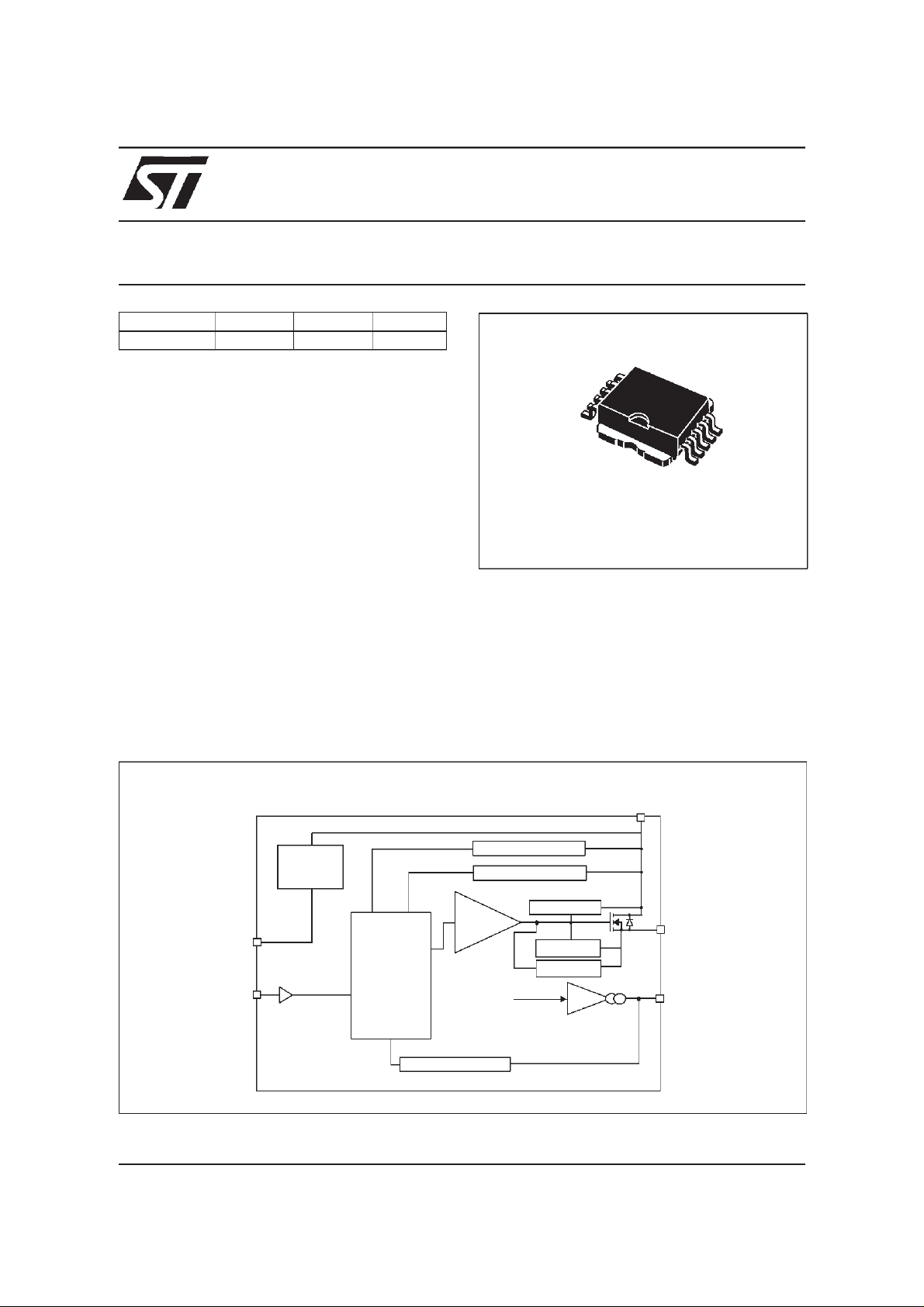
BLOCK DIAGRAM
I
OUT
CC
V
CC
pin
CC
VN610SP
TARGET SPECIFICATION
10
1
PowerSO-10
voltage clamp protects the device against low
energy spikes (see ISO7637 transient
compatibility table). This device integrates an
analog current sense which delivers a current
proportional to the load current (according to a
known ratio). Active current limitation combined
with thermal shut-down and automatic restart
protect the device against overload. Device
automatically turns off in case of ground pin
disconnection.
V
CC
V
CC
CLAMP
GND
LOGIC
INPUT
OVERTEMP.
(*) See application schematic at page 8
September 1999 1/10
OVERVOLTAGE
UNDERVOLTAGE
DRIVER
PwCLAMP
I
OUT
I
V
DSLIM
LIM
OUTPUT
K
CURRENT
SENSE
1

VN610SP
ABSOLUTE MAXIMUM RATING
Symbol Parameter Value Unit
V
-V
-I
GND
I
OUT
-I
OUT
I
V
CSENSE
V
ESD
P
TOT
T
T
T
STG
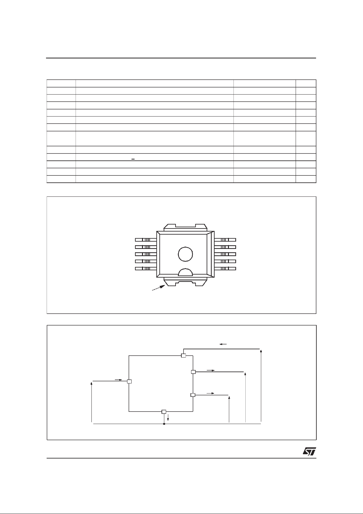
CONNECTION DIAGRAM (TOP VIEW)
DC supply voltage 41 V
CC
Reverse DC supply voltage -0.3 V
CC
DC reverse ground pin current -200 mA
DC output current Internally limited A
Reverse DC output current -50 A
DC input current +/- 10 mA
IN
Current sense maximum voltage
-3
+15
Electrostatic discharge (R=1.5kΩ; C=100pF) 2000 V
Power dissipation at TC<25°C 125 W
Junction operating temperature Internally limited °C
j
Case operating temperature -40 to 150 °C
c
Storage temperature -55 to 150 °C
V
V
GROUND
INPUT
C.SENSE
N.C.
N.C.
V
CC
CURRENT AND VOLTAGECONVENTIONS
I
IN
V
IN
INPUT
CURRENT SENSE
6
7
8
9
10
GND
11
V
CC
OUTPUT
I
GND
5
4
3
2
1
I
OUT
I
SENSE
V
SENSE
OUTPUT
OUTPUT
OUTPUT
OUTPUT
OUTPUT
I
CC
V
CC
V
OUT
2/10
1

VN610SP
THERMAL DATA
Symbol Parameter Value Unit
R
thj-case
R
thj-amb
Thermal resistance junction-case (MAX) 1 °C/W
Thermal resistance junction-ambient (MAX) 50 °C/W
ELECTRICAL CHARACTERISTICS(8V<V
<36V; -40°C<Tj<150°C; unless otherwise specified)
CC
POWER
Symbol Parameter Test Conditions Min Typ Max Unit
V
V
V
R
V
clamp
I
L(off)
Note 1: V
CC
USD
OV
ON
I
S
Operating supply
voltage
5.5 13 36 V
Undervoltage shutdown 3 4 5.5 V
Overvoltage shutdown (See Note 1) 36 42 48 V
I
=15A; Tj=25oC
OUT
On state resistance
Clamp Voltage
Supply current
Off state output current VIN=V
and VOVare correlated. Typical difference is 5V.
clamp
=15A; Tj=150oC
I
OUT
I
=9A; VCC=6V
OUT
=20 mA
I
CC
(see note 1)
Off state; INPUT= n.c.; V
CC
=13V
On state; VIN=5V; VCC=13V; I
=3.9K
R
SENSE
=0V 0 50 µA
OUT
OUT
41 48 55 V
=0A;
10
20
35
25
5
SWITCHING (VCC=13V)
Symbol Parameter Test Conditions Min Typ Max Unit
(dV
(dV
t
d(on)
t
d(off)
OUT
OUT
W
W
ON
OFF
Turn-on delay time R1=0.87Ω 50 µs
Turn-on delay time R1=0.87Ω 50 µs
/dt)onTurn-on voltage slope R1=0.87Ω 0.3 V/µs
/dt)
Turn-off voltage slope R1=0.87Ω 0.3 V/µs
off
Switching losses
energy at turn-on
Switching losses
energy at turn-off
R1=2.6Ω 1.0 mJ
R1=2.6Ω 0.5 mJ
mΩ
mΩ
mΩ
µA
mA
PROTECTIONS
Symbol Parameter Test Conditions Min Typ Max Unit
I
lim
T
TSD
T
T
HYST
V
DEMAG
V
ON
=13V
V
DC Short circuit current
CC
5.5V<V
CC
<36V
Thermal shutdown
temperature
Thermal reset
R
temperature
Thermal hysteresis 7 15 °C
I
Turn-off output voltage
=2A; VIN=0; L=6mH
OUT
clamp
Output voltage drop
limitation
I
=1.5A
OUT
=-40°C...+150°C
T
j
45 75 120
120
150 175 200 °C
135 °C
Vcc-41 Vcc-48 Vcc-55 V
50 mV
A
A
3/10
1
 Loading...