

VN05NSP
HIGH SIDE SMART POWER SOLID STATE RELAY
TYPE V
VN05 NS P 60 V 0.18 Ω 13 A 26 V
■ OUTPUTCURRENT(CONTINUOUS):
13 A @ T
■ 5 V LOGIC LEVEL COMPATIBLEINPUT
■ THERMALSHUT-DOWN
■ UNDERVOLTAGE SHUT-DOWN
■ OPENDRAIN DIAGNOSTIC OUTPUT
■ VERY LOW STAND-BY POWER
DSS
=25oC
c
R
DS(on)
I
OUT
V
CC
DISSIPATION
DESCRIPTION
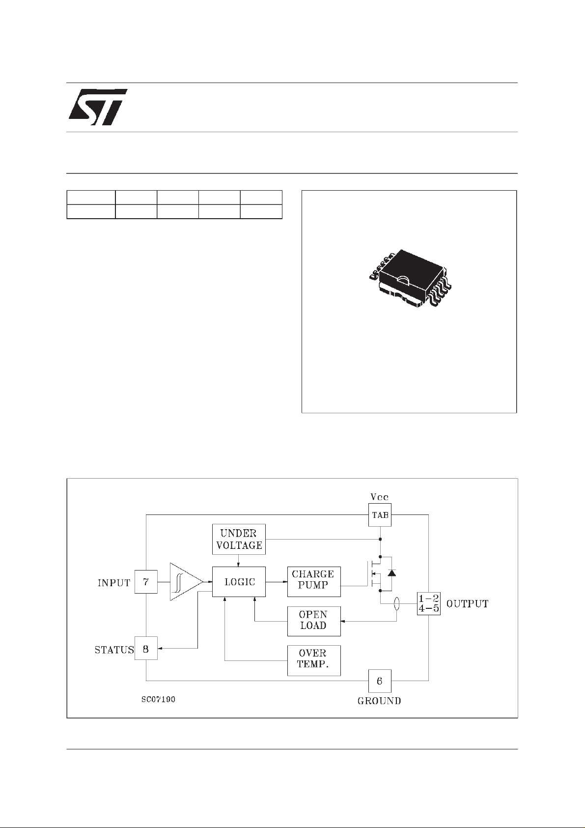
The VN05NSP is a monolithic devices made
using STMicroelectronics VIPower Technology,
intended for driving resistive or inductive loads
with one side grounded.
Built-in thermal shut-down protects the chip from
over temperature and short circuit.
The input control is 5V logic level compatible.
The open drain diagnostic output indicates open
circuit(no load) andover temperaturestatus.
BLOCK DIAGRAM
10
1
PowerSO-10
June 1998
1/9
VN05NSP
ABSOLUTEMAXIMUMRATING
Symbol Parameter Value Unit
V
(BR)DSS
I
OUT
I
I
-V
I
STAT
V
ESD
P
T
T
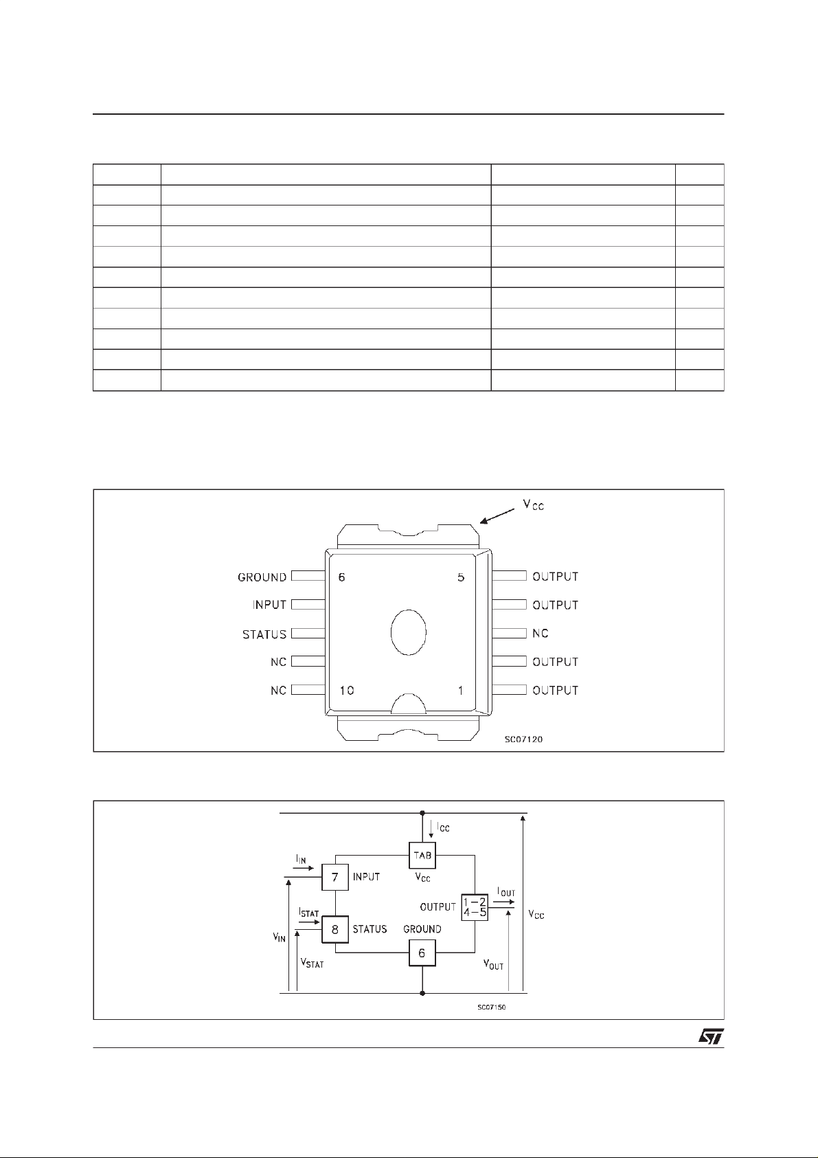
CONNECTIONDIAGRAMS
Drain-S o ur ce Breakdown V olt age 60 V
Out put Cu r rent (cont. ) 13 A
Revers e Out put Current -13 A
R
Input Current ±10 mA
IN
Reverse Supply V oltage -4 V
CC
St at us Cur rent ±10 mA
Elect r o st at ic Dischar ge (1.5 kΩ, 100 pF ) 2000 V
Power Dissipation at Tc≤ 25oC56W
tot
Junction O perat in g T em pe r at ure -40 t o 150
j
St orage Tem per atur e -55 t o 150
stg
o
C
o
C
CURRENT ANDVOLTAGE CONVENTIONS
2/9
VN05NSP
THERMALDATA
R
thj-case
R
thj- amb
($) When mounted using minimum recommended pad size on FR-4 board
ELECTRICAL CHARACTERISTICS (VCC=13 V; -40 ≤ Tj≤ 125oC unless otherwisespecified)
POWER
Symbol Parameter Test Condition s Min. Typ. Max. Unit
V
R
I
SWITCHING
Symbol Parameter Test Condition s Min. Typ. Max. Unit
t
d(on)
t
d(off)
(di/dt)
(di/dt)
Ther mal Resis t ance Junc t io n-c ase Max
Therm al Res is tance J unction-ambient ($) Max
Supply Voltage 7 26 V
CC
On Stat e Resist a nce I
on
Supply Current Of f Stat e Tj≥ 25oC
S
=6A
OUT
=6A Tj=25oC
I
OUT
2.2
50
On State
Turn-on Delay Time Of
Out put Cu r rent
Rise TimeOf Output
t
r
Current
Turn-off Delay Time Of
Out put Cu r rent
Fall T ime Of Output
t
f
Current
Tur n-on Current S lope I
on
Tur n-of f C urrent Slope I
off
I
= 6 A Res istive Load
OUT
Input Rise Time < 0.1 µsT
I
= 6 A Res istive Load
OUT
Input Rise Time < 0.1 µsT
I
= 6 A Res istive Load
OUT
Input Rise Time < 0.1 µsT
I
= 6 A Res istive Load
OUT
Input Rise Time < 0.1 µsT
=6A
OUT
I
OUT=IOV
=6A
OUT
I
OUT=IOV
j
j
j
j
=25oC
=25oC
=25oC
=25oC
15 µs
30 µs
20 µs
10 µs
0.36
0.18
50
15
0.52A/µs
2
4
o
C/W
o
C/W
Ω
Ω
µA
mA
A/µs
A/µs
A/µs
LOGIC INPUT
Symbol Parameter Test Condition s Min. Typ. Max. Unit
V
Input Low Level
IL
0.8 V
Volt age
V
Input Hig h Lev el
IH
2(*)V
Volt age
V
I(hyst.)
Input Hysteresis
0.5 V
Volt age
I
V
Input Current VIN= 5 V 250 5 00 µA
IN
Input Cla m p Volt ag e IIN=10mA
ICL
=-10mA
I
IN
6
-0.7
PROTECTIONS AND DIAGNOSTICS
Symbol Parameter Test Condition s Min. Typ. Max. Unit
V
(•) St at us V oltage Output
STAT
Low
V
USD
Under Voltage Shut
Down
I
=1.6mA 0.4 V
STAT
6.5 V
V
V
3/9
 Loading...