

HIGH SIDE SMART POWER SOLID STATE RELAY
TYPE V
VN02NSP 60 V 0.4 Ω 6 A 26 V
VN02NPT 60 V 0.4 Ω 6 A 26 V
■ OUTPUT CURRENT (CONTINUOUS):
6A @ T
■ 5V LOGIC LEVEL COMPATIBLE INPUT
■ THERMAL SHUT-DOWN
■ UNDER VOLTAGE SHUT- DO WN
■ OPEN DRAIN DIAGNOSTIC OUTPUT
■ VERY LOW STAND-BY POWER
=25oC
c
DSS
DISSIPATION
R
DS(on
)I
OUT
V
VN02NSP
VN02NPT
PRELIMINARY DATA
CC
10
1
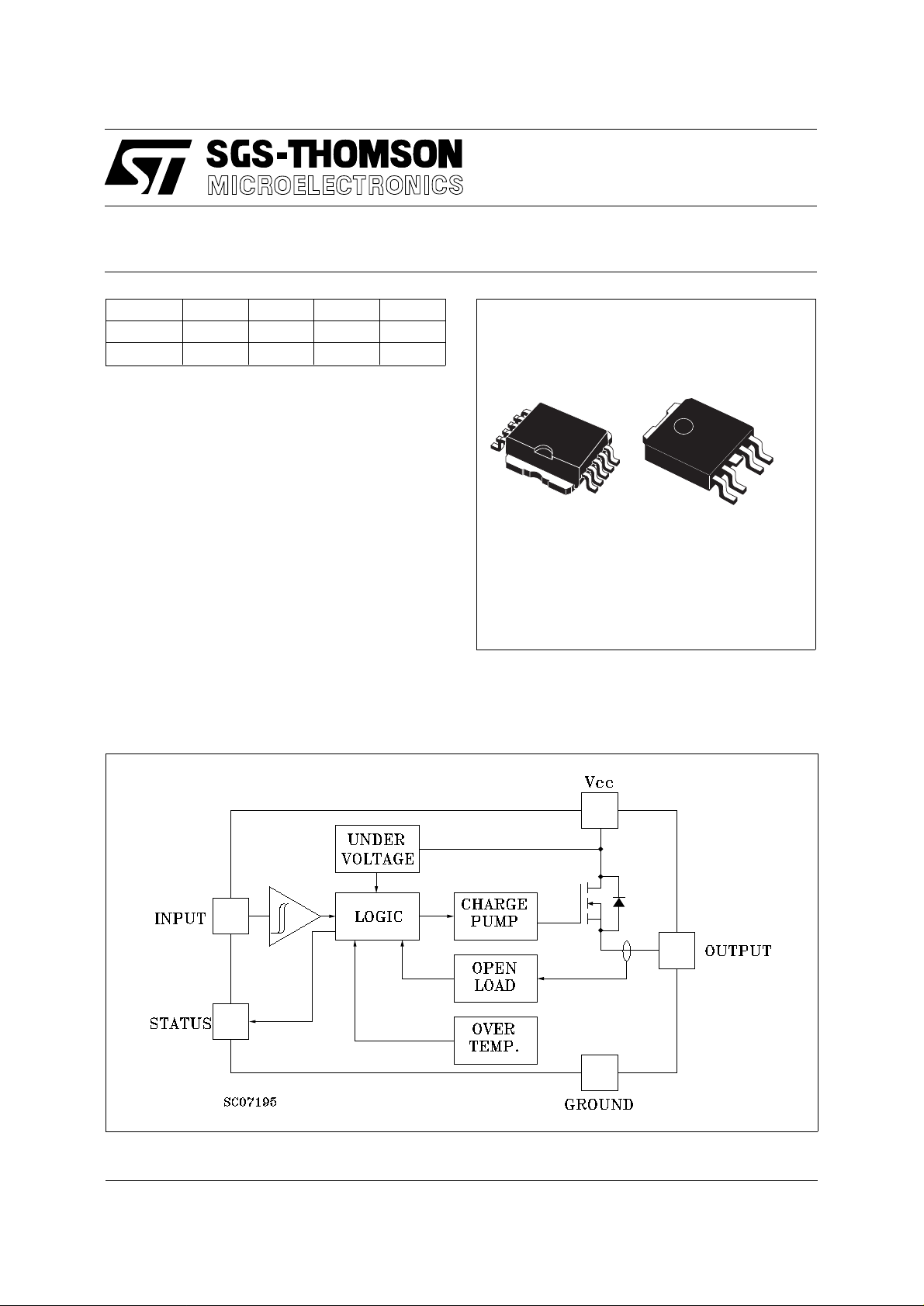
DESCRIP TION
The VN02NSP/VN02NPT are monolithic devices
made using SGS-THOMSON Vertical Intelligent
Power Technology, intended for driving resistive
or inductive loads with one side grounded.
Built-in thermal shut-down protects the chip from
over temperature and short circ uit.
The input control is 5V logic level compatible.
BLOCK DIAG RAM
PowerSO-10TM PPAK
The open drain diagnostic output indicates open
circuit (no load) and over temperature status.
September 1997
1/10

VN02NSP/VN02NPT
ABSOLUTE MAXIMUM RATING
Symbol Parameter Value Unit
PowerSO-10 PPAK
V
(BR)DSS
I
OUT
I
I
-V
I
STAT
V
ESD
P
T
T
CONNECTION DIAGRAMS
Drain-Source Breakdown Voltage 60 V
Output Current (cont.) 6 A
Reverse Output Current -6 A
R
Input Current ±10 mA
IN
Reverse Supply Voltage -4 V
CC
Status Current ±10 mA
Electrostatic Discharge (1.5 kΩ, 100 pF)
Power Dissipation at Tc ≤ 25 oC
tot
Junction Operating Temperature -40 to 150
j
Storage Temperature -55 to 150
stg
2000 V
58 46 W
o
C
o
C
CURRENT AND VOLTAGE CONVENTI ONS
2/10

VN02NSP/VN02NPT
THERMAL DATA
PowerSO-10 PPAK
R
thj-case
R
thj-amb
($) When mounted using minimum recommended pad size on FR-4 board
ELECTRICAL CHARACTERISTICS (VCC = 13 V; -40 ≤ Tj ≤ 125 oC unless otherwise specified)
POWER
Symbol Parameter Test Conditions Min. Typ. Max. Unit
V
R
I
SWITCHING
Symbol Parameter Test Conditions Min. Typ. Max. Unit
t
d(on)
t
d(off)
(di/dt)
(di/dt)
Thermal Resistance Junction-case Max
Thermal Resistance Junction-ambient ($) Max
Supply Voltage 7 26 V
CC
On State Resistance I
on
Supply Current
S
= 3 A
OUT
I
= 3 A Tj = 25 oC
OUT
Off State T
≥ 25 oC
j
2.14
62.5
On State
Turn-on Delay Time Of
Output Current
t
Rise Time Of Output
r
Current
Turn-off Delay Time Of
Output Current
t
Fall Time Of Output
f
Current
Turn-on Current Slope I
on
Turn-off Current Slope I
off
I
= 3 A Resistive Load
OUT
Input Rise Time < 0.1 µs T
I
= 3 A Resistive Load
OUT
Input Rise Time < 0.1 µs T
I
= 3 A Resistive Load
OUT
Input Rise Time < 0.1 µs T
I
= 3 A Resistive Load
OUT
Input Rise Time < 0.1 µs T
= 3 A
OUT
I
= IOV
OUT
= 3 A
OUT
I
= I
OUT
OV
= 25 oC
j
= 25 oC
j
= 25 oC
j
= 25 oC
j
10 µs
15 µs
15 µs
6 µs
3.33
100
0.8
0.4
50
15
0.52A/µs
2
4
o
C/W
o
C/W
Ω
Ω
µA
mA
A/µs
A/µs
A/µs
LOGIC INP UT
Symbol Parameter Test Conditions Min. Typ. Max. Unit
V
V
V
I(hyst.)
I
V
Input Low Level
IL
Voltage
Input High Level
IH
2(*)V
Voltage
Input Hysteresis
0.5 V
Voltage
Input Current VIN = 5 V 250 500 µA
IN
Input Clamp Voltage IIN = 10 mA
ICL
I
= -10 mA
IN
6
-0.7
0.8 V
V
V
3/10
 Loading...