

SGS Thomson Microelectronics VN02HSP13TR Datasheet

®
HIGH SIDE SMART POWER SOLID STATE RELAY
TYPE V
VN02HSP 60 V 0.4 Ω 6 A 36 V
■ OUTPUT CURRENT (CONTINUOUS):
6A @ T
■ 5V LOGIC LEVEL COMPATIBLE INPUT
■ THERMAL SHUT-DOWN
■ UNDER VOLTAGE SHUT- DO WN
■ OPEN DRAIN DIAGNOSTIC OUTPUT
■ VERY LOW STAND-BY POWER
=25oC
c
DSS
DISSIPATION
DESCRIP TION
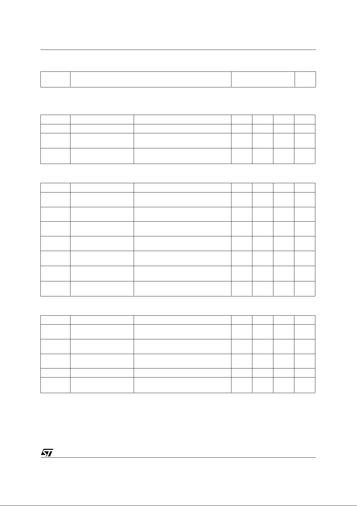
The VN02HSP is a monolithic devices made
using STMicroelectronics VIPower Technology,
intended for driving resistive or inductive loads
with one side grounded.
Built-in thermal shut-down protects the chip from
over temperature and short circ uit.
The input control is 5V logic level compatible.
The open drain diagnostic output indicates open
circuit (no load) and over temperature stat us.
R
DS(on
)I
OUT
V
CC
VN02HSP
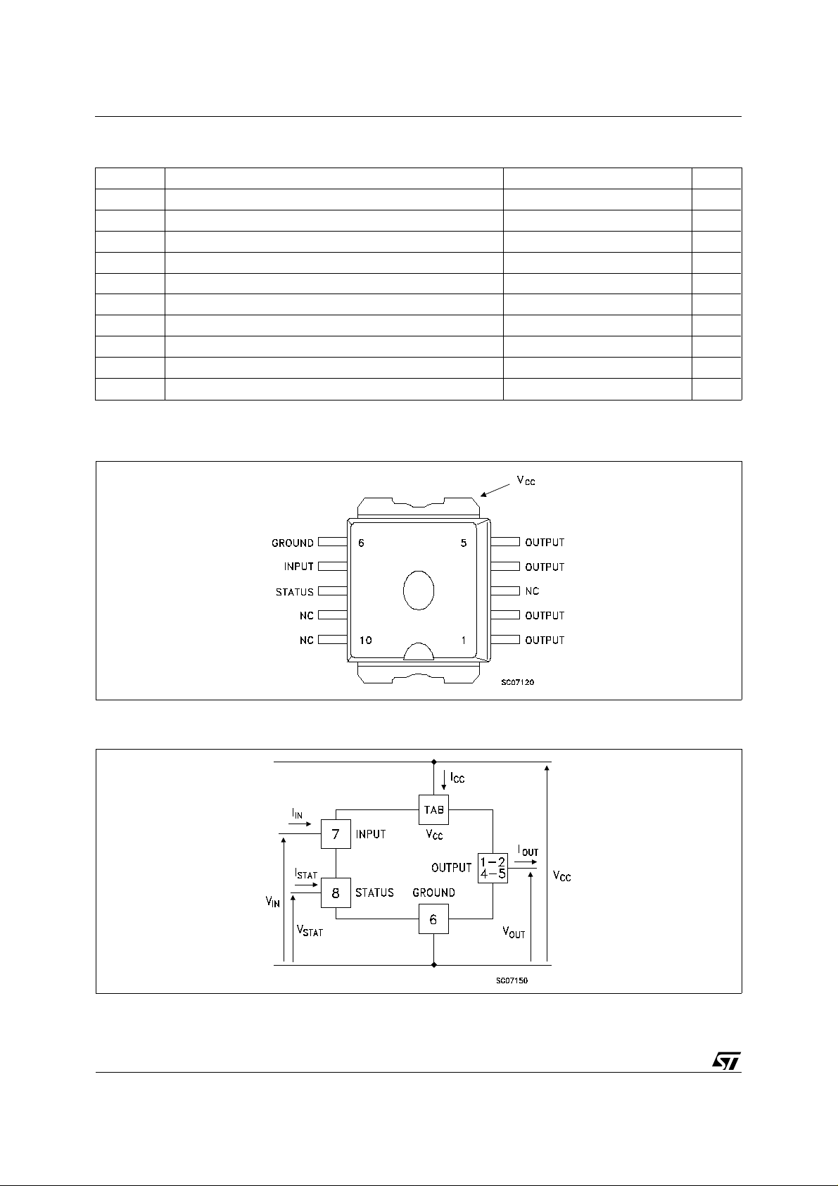
10
1
PowerSO-10
BLOCK DIAG RAM
August 1998
1/8
VN02HSP
ABSOLUTE MAXIMUM RATING
Symbol Parameter Value Unit
V
(BR)DSS
I
OUT
I
I
-V
I
STAT
V
ESD
P
T
T
CONNECTION DIAGRAMS
Drain-Source Breakdown Voltage 60 V
Output Current (cont.) 6 A
Reverse Output Current -6 A
R
Input Current ±10 mA
IN
Reverse Supply Voltage -4 V
CC
Status Current ±10 mA
Electrostatic Discharge (1.5 kΩ, 100 pF) 2000 V
Power Dissipation at Tc ≤ 25 oC 29 W
tot
Junction Operating Temperature -40 to 150
j
Storage Temperature -55 to 150
stg
o
C
o
C
CURRENT AND VOLTAGE CONVENTI ONS
2/8
VN02HSP
THERMAL DATA
50
20
o
C/W
o
C/W
µA
mA
A/µs
A/µs
4
A/µs
R
thj-case
R
thj-amb
Thermal Resistance Junction-case Max
Thermal Resistance Junction-ambient Max
4.35
50
ELECTRICAL CHARACTERISTICS (VCC = 9 to 36 V; -40 ≤ Tj ≤ 125 oC unless otherwise specified)
POWER
Symbol Parameter Test Conditions Min. Typ. Max. Unit
V
R
I
Supply Voltage see note 1 5 36 V
CC
On State Resistance I
on
Supply Current Off State Tj ≥ 25 oC
S
= 3 A
OUT
I
= 3 A Tj = 25 oC
OUT
0.8
0.4
On State
SWITCHING
Symbol Parameter Test Conditions Min. Typ. Max. Unit
t
d(on)
t
d(off)
(di/dt)
(di/dt)
V
demag
Turn-on Delay Time Of
Output Current
t
Rise Time Of Output
r
Current
Turn-off Delay Time Of
Output Current
t
Fall Time Of Output
f
Current
Turn-on Current Slope I
on
Turn-off Current Slope I
off
Inductive Load Clamp
Voltage
I
= 3 A Resistive Load
OUT
Input Rise Time < 0.1 µs T
I
= 3 A Resistive Load
OUT
Input Rise Time < 0.1 µs T
I
= 3 A Resistive Load
OUT
Input Rise Time < 0.1 µs T
I
= 3 A Resistive Load
OUT
Input Rise Time < 0.1 µs T
= 3 A
OUT
I
= IOV 25 ≤ Tj ≤ 140 oC
OUT
= 3 A
OUT
I
= IOV 25 ≤ Tj ≤ 140 oC
OUT
I
= 3 A L = 1 mH -7 -4 -2 V
OUT
= 25 oC
j
= 25 oC
j
= 25 oC
j
= 25 oC
j
51020µs
51545µs
51530µs
2615µs
0.05 0.15 0.52A/µs
0.1 0.4 2
Ω
Ω
LOGIC INP UT
Symbol Parameter Test Conditions Min. Typ. Max. Unit
V
V
V
I(hyst.)
I
V
Input Low Level
IL
Voltage
Input High Level
IH
2(*)V
Voltage
Input Hysteresis
0.5 V
Voltage
Input Current VIN = 5 V 250 500 µA
IN
Input Clamp Voltage IIN = 10 mA
ICL
I
= -10 mA
IN
5.5 6
-0.7 -0.3
0.8 V
V
V
3/8
 Loading...