

VN02AN
HIGH SIDE SMART POWER SOLID STATE RELAY
TYPE V
VN02AN 60 V 0.35 Ω 7A 36V
■ OUTPUTCURRENT(CONTINUOUS):
7A @ T
■ LOGICLEVEL5V COMPATIBLEINPUT
■ THERMALSHUT-DOWN
■ UNDERVOLTAGE PROTECTION
■ OPENDRAINDIAGNOSTIC OUTPUT
■ FAST DEMAGNETIZATIONOF INDUCTIVE
=25oC
c
DSS
R
DS(on
)I
OUT
V
CC
LOAD
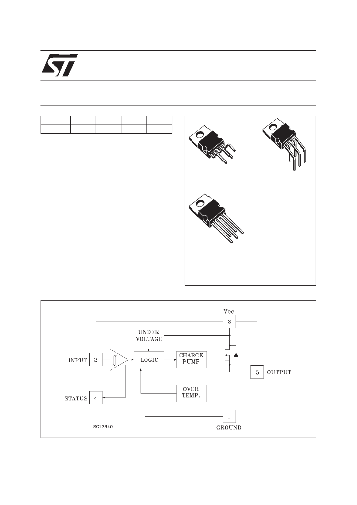
DESCRIPTION
The VN02AN is a monolithic device made using
STMicroelectronics VIPower Technology,
intended for driving resistive or inductive loads
with one side grounded.
Built-in thermal shut-down protects the chip from
over temperatureand short circuit.
The diagnostic output indicates an over
temperaturestatus.
Fast turn-off of inductive load is achieved by
negative (-18 V) load voltage at turn-off.
BLOCK DIAGRAM
PENTAWATT
(vertical)
PENTAWATT
(horizontal)
PENTAWATT
(in-line)
ORDER CODES:
PENTAWATTvertical VN02AN
PENTAWATThorizontal VN02AN(011Y)
PENTAWATTin-line VN02AN(012Y)
July 1998
1/11
VN02AN
ABSOLUTEMAXIMUMRATING
Symbol Parameter Value Unit
V
(BR)DSS
I
OUT
I
I
-V
I
STAT
V
ESD
P
T
T
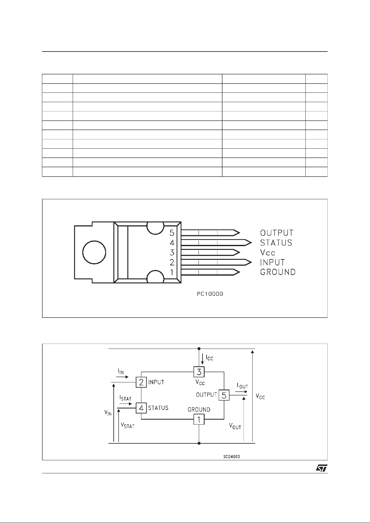
CONNECTIONDIAGRAMS
Drain-S o ur ce Breakdown V olt ag e 60 V
Out put Cur rent (cont. ) 7 A
Reverse Output Cu rrent -7 A
R
Input Cur rent ±10 mA
IN
Reverse Supply V oltage -4 V
CC
St at us Current (sink) ±10 mA
Elect r o st at ic Discharge ( 1. 5 kΩ, 100 pF) 2000 V
Power Dissipation at Tc≤ 25oC31W
tot
Junction Operat ing Tempe r at ur e -40 t o 150
j
St orage Tem per atur e -55 t o 150
stg
o
C
o
C
CURRENT ANDVOLTAGECONVENTIONS
2/11
THERMALDATA
R
thj-case
R
thj- amb
Ther mal Resis t an ce Junction-cas e Max
Ther mal Resis t an ce Junction-ambien t Max
60
VN02AN
4
o
C/W
o
C/W
ELECTRICAL CHARACTERISTICS (VCC=9 to 36 V; T
=25oC unless otherwise specified)
case
POWER
Symbol Parameter Test C ondition s Min. Typ. Max. Unit
V
* Supply Voltag e -40oC<Tj< 125oC736V
CC
R
I
On Stat e Re si st ance I
on
Supply C ur rent Of f State VCC=30V
S
=3A
OUT
=1A VCC=30V Tj=125oC
I
OUT
On State V
On State V
=30V
CC
=30V Tj= 125oC
CC
0.35
0.6
1
9
7
SWITCHING
Symbol Parameter Test C ondition s Min. Typ. Max. Unit
t
d(on)
t
d(off)
(di/dt)
(di/dt)
V
DEMAG
Turn-on Delay Time Of
Out put Cur rent
Rise TimeOf Output
t
r
Current
Turn-off Delay T ime O f
Out put Cur rent
Fall T ime Of Output
t
f
Current
Tur n-on C ur rent S lope I
on
Tur n-of f Curr ent S lope I
off
Induc t i ve Load Clam p
Volt age
I
= 3 A Resistive Load
OUT
15 µs
Input Ris e Time < 0.1 µs
I
= 3 A Resistive Load
OUT
15 µs
Input Ris e Time < 0.1 µs
I
= 3 A Resistive Load
OUT
14 µs
Input Ris e Time < 0.1 µs
I
= 3 A Resistive Load
OUT
4.5 µs
Input Ris e Time < 0.1 µs
=3A 25oC<Tj<125oC
OUT
I
OUT=IOV
=3A 25oC<Tj<125oC
OUT
I
OUT=IOV
I
=3A -40oC<Tj<125oC -24 -18 -14 V
OUT
25oC<Tj<125oC
25oC<Tj<125oC
0.51A/µs
1.54A/µs
Ω
Ω
mA
mA
mA
A/µs
A/µs
LOGIC INPUT (-40oC ≤ Tj≤ 125oC unless otherwisespecified)
Symbol Parameter Test C ondition s Min. Typ. Max. Unit
V
V
V
I(hyst.)
I
V
Input Low Level
IL
Volt age
Input Hig h Level
IH
Volt age
Input Hysteresis
Volt age
Input Cur rent VIN=5V
IN
Input Cla mp Volt ag e IIN=10mA
ICL
=2V
V
IN
=0.8V 25
V
IN
I
=-10mA
IN
0.8 V
2(*)V
0.5 V
250 600
300
5.5 6
-0.7 -0.3
µA
µA
µA
V
V
3/11
VN02AN
ELECTRICAL CHARACTERISTICS (continued)
o
PROTECTION AND DIAGNOSTICS(-40
C ≤ Tj≤ 125oC unless otherwisespecified)
Symbol Parameter Test C ondition s Min. Typ. Max. Unit
V
STAT
St at us Volt age Out put
I
=1.6mA 0.4 V
STAT
Low
I
STAT
V
USD
St at us Leakage Cu rre nt V
Under Vol ta ge Shut
=5V 10 µA
STAT
3.5 6 7 V
Down
V
SCL
I
OV
I
St at us Clamp Volt age I
Over Current R
Aver age Current In
av
=10mA
STAT
I
=-10mA
STAT
<10mΩ 15 A
LOAD
R
<10mΩ Tc=85oC0.6A
LOAD
5.5 6
-0.7 -0.3
V
V
Short Circuit
I
DOFF
T
TSD
Leakage Current VCC=30V 1 mA
Ther mal Shut-d own
140
o
Tem perature
T
(*) The Vih is internallyclamped at about 6V. It is possible to connect this pin to a higher voltagevia an external resistor calculated to not
exceed 10 mA at the input pin.
Reset Temperatu r e 125
R
o
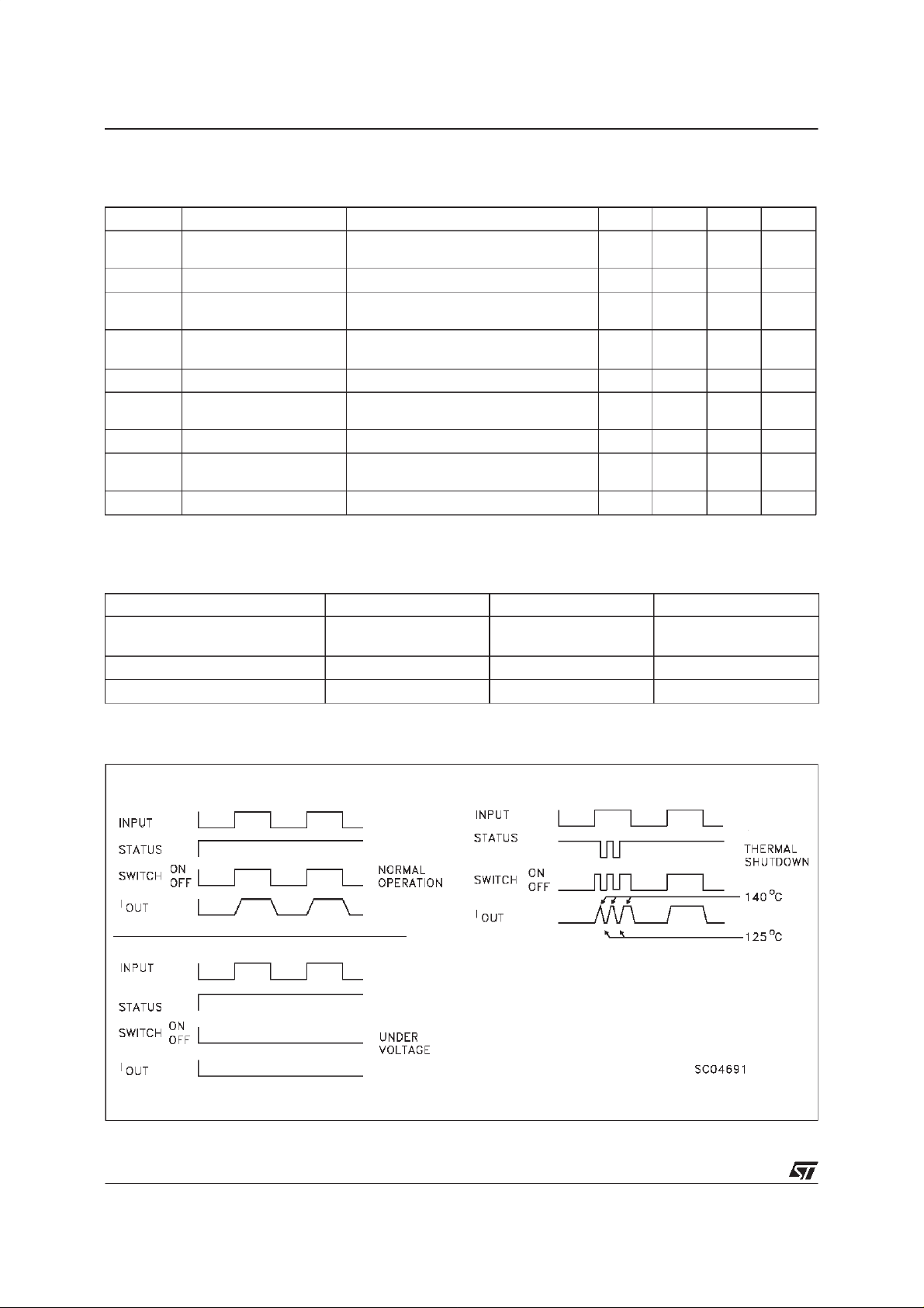
TRUTH TABLE
INPUT DIAGNOSTIC OUTPUT
Normal Opera ti on L
H
Ov er- temperature H L L
Under-voltage X H L
H
H
L
H
C
C
Figure1: Waveforms
4/11
 Loading...